US12110591B2 - Susceptor arrangement of a CVD reactor - Google Patents
Susceptor arrangement of a CVD reactor Download PDFInfo
- Publication number
- US12110591B2 US12110591B2 US17/593,081 US202017593081A US12110591B2 US 12110591 B2 US12110591 B2 US 12110591B2 US 202017593081 A US202017593081 A US 202017593081A US 12110591 B2 US12110591 B2 US 12110591B2
- Authority
- US
- United States
- Prior art keywords
- covering plate
- susceptor
- covering
- lowermost
- uppermost
- Prior art date
- Legal status (The legal status is an assumption and is not a legal conclusion. Google has not performed a legal analysis and makes no representation as to the accuracy of the status listed.)
- Active, expires
Links
Images




Classifications
-
- C—CHEMISTRY; METALLURGY
- C23—COATING METALLIC MATERIAL; COATING MATERIAL WITH METALLIC MATERIAL; CHEMICAL SURFACE TREATMENT; DIFFUSION TREATMENT OF METALLIC MATERIAL; COATING BY VACUUM EVAPORATION, BY SPUTTERING, BY ION IMPLANTATION OR BY CHEMICAL VAPOUR DEPOSITION, IN GENERAL; INHIBITING CORROSION OF METALLIC MATERIAL OR INCRUSTATION IN GENERAL
- C23C—COATING METALLIC MATERIAL; COATING MATERIAL WITH METALLIC MATERIAL; SURFACE TREATMENT OF METALLIC MATERIAL BY DIFFUSION INTO THE SURFACE, BY CHEMICAL CONVERSION OR SUBSTITUTION; COATING BY VACUUM EVAPORATION, BY SPUTTERING, BY ION IMPLANTATION OR BY CHEMICAL VAPOUR DEPOSITION, IN GENERAL
- C23C16/00—Chemical coating by decomposition of gaseous compounds, without leaving reaction products of surface material in the coating, i.e. chemical vapour deposition [CVD] processes
- C23C16/44—Chemical coating by decomposition of gaseous compounds, without leaving reaction products of surface material in the coating, i.e. chemical vapour deposition [CVD] processes characterised by the method of coating
- C23C16/46—Chemical coating by decomposition of gaseous compounds, without leaving reaction products of surface material in the coating, i.e. chemical vapour deposition [CVD] processes characterised by the method of coating characterised by the method used for heating the substrate
-
- C—CHEMISTRY; METALLURGY
- C23—COATING METALLIC MATERIAL; COATING MATERIAL WITH METALLIC MATERIAL; CHEMICAL SURFACE TREATMENT; DIFFUSION TREATMENT OF METALLIC MATERIAL; COATING BY VACUUM EVAPORATION, BY SPUTTERING, BY ION IMPLANTATION OR BY CHEMICAL VAPOUR DEPOSITION, IN GENERAL; INHIBITING CORROSION OF METALLIC MATERIAL OR INCRUSTATION IN GENERAL
- C23C—COATING METALLIC MATERIAL; COATING MATERIAL WITH METALLIC MATERIAL; SURFACE TREATMENT OF METALLIC MATERIAL BY DIFFUSION INTO THE SURFACE, BY CHEMICAL CONVERSION OR SUBSTITUTION; COATING BY VACUUM EVAPORATION, BY SPUTTERING, BY ION IMPLANTATION OR BY CHEMICAL VAPOUR DEPOSITION, IN GENERAL
- C23C14/00—Coating by vacuum evaporation, by sputtering or by ion implantation of the coating forming material
- C23C14/22—Coating by vacuum evaporation, by sputtering or by ion implantation of the coating forming material characterised by the process of coating
- C23C14/50—Substrate holders
- C23C14/505—Substrate holders for rotation of the substrates
-
- C—CHEMISTRY; METALLURGY
- C23—COATING METALLIC MATERIAL; COATING MATERIAL WITH METALLIC MATERIAL; CHEMICAL SURFACE TREATMENT; DIFFUSION TREATMENT OF METALLIC MATERIAL; COATING BY VACUUM EVAPORATION, BY SPUTTERING, BY ION IMPLANTATION OR BY CHEMICAL VAPOUR DEPOSITION, IN GENERAL; INHIBITING CORROSION OF METALLIC MATERIAL OR INCRUSTATION IN GENERAL
- C23C—COATING METALLIC MATERIAL; COATING MATERIAL WITH METALLIC MATERIAL; SURFACE TREATMENT OF METALLIC MATERIAL BY DIFFUSION INTO THE SURFACE, BY CHEMICAL CONVERSION OR SUBSTITUTION; COATING BY VACUUM EVAPORATION, BY SPUTTERING, BY ION IMPLANTATION OR BY CHEMICAL VAPOUR DEPOSITION, IN GENERAL
- C23C16/00—Chemical coating by decomposition of gaseous compounds, without leaving reaction products of surface material in the coating, i.e. chemical vapour deposition [CVD] processes
- C23C16/44—Chemical coating by decomposition of gaseous compounds, without leaving reaction products of surface material in the coating, i.e. chemical vapour deposition [CVD] processes characterised by the method of coating
- C23C16/458—Chemical coating by decomposition of gaseous compounds, without leaving reaction products of surface material in the coating, i.e. chemical vapour deposition [CVD] processes characterised by the method of coating characterised by the method used for supporting substrates in the reaction chamber
- C23C16/4582—Rigid and flat substrates, e.g. plates or discs
- C23C16/4583—Rigid and flat substrates, e.g. plates or discs the substrate being supported substantially horizontally
- C23C16/4584—Rigid and flat substrates, e.g. plates or discs the substrate being supported substantially horizontally the substrate being rotated
-
- C—CHEMISTRY; METALLURGY
- C23—COATING METALLIC MATERIAL; COATING MATERIAL WITH METALLIC MATERIAL; CHEMICAL SURFACE TREATMENT; DIFFUSION TREATMENT OF METALLIC MATERIAL; COATING BY VACUUM EVAPORATION, BY SPUTTERING, BY ION IMPLANTATION OR BY CHEMICAL VAPOUR DEPOSITION, IN GENERAL; INHIBITING CORROSION OF METALLIC MATERIAL OR INCRUSTATION IN GENERAL
- C23C—COATING METALLIC MATERIAL; COATING MATERIAL WITH METALLIC MATERIAL; SURFACE TREATMENT OF METALLIC MATERIAL BY DIFFUSION INTO THE SURFACE, BY CHEMICAL CONVERSION OR SUBSTITUTION; COATING BY VACUUM EVAPORATION, BY SPUTTERING, BY ION IMPLANTATION OR BY CHEMICAL VAPOUR DEPOSITION, IN GENERAL
- C23C16/00—Chemical coating by decomposition of gaseous compounds, without leaving reaction products of surface material in the coating, i.e. chemical vapour deposition [CVD] processes
- C23C16/44—Chemical coating by decomposition of gaseous compounds, without leaving reaction products of surface material in the coating, i.e. chemical vapour deposition [CVD] processes characterised by the method of coating
- C23C16/458—Chemical coating by decomposition of gaseous compounds, without leaving reaction products of surface material in the coating, i.e. chemical vapour deposition [CVD] processes characterised by the method of coating characterised by the method used for supporting substrates in the reaction chamber
- C23C16/4582—Rigid and flat substrates, e.g. plates or discs
- C23C16/4583—Rigid and flat substrates, e.g. plates or discs the substrate being supported substantially horizontally
- C23C16/4585—Devices at or outside the perimeter of the substrate support, e.g. clamping rings, shrouds
-
- C—CHEMISTRY; METALLURGY
- C30—CRYSTAL GROWTH
- C30B—SINGLE-CRYSTAL GROWTH; UNIDIRECTIONAL SOLIDIFICATION OF EUTECTIC MATERIAL OR UNIDIRECTIONAL DEMIXING OF EUTECTOID MATERIAL; REFINING BY ZONE-MELTING OF MATERIAL; PRODUCTION OF A HOMOGENEOUS POLYCRYSTALLINE MATERIAL WITH DEFINED STRUCTURE; SINGLE CRYSTALS OR HOMOGENEOUS POLYCRYSTALLINE MATERIAL WITH DEFINED STRUCTURE; AFTER-TREATMENT OF SINGLE CRYSTALS OR A HOMOGENEOUS POLYCRYSTALLINE MATERIAL WITH DEFINED STRUCTURE; APPARATUS THEREFOR
- C30B25/00—Single-crystal growth by chemical reaction of reactive gases, e.g. chemical vapour-deposition growth
- C30B25/02—Epitaxial-layer growth
- C30B25/12—Substrate holders or susceptors
-
- H01L21/68735—
-
- H01L21/68757—
-
- H01L21/68771—
-
- H01L21/68785—
-
- H—ELECTRICITY
- H10—SEMICONDUCTOR DEVICES; ELECTRIC SOLID-STATE DEVICES NOT OTHERWISE PROVIDED FOR
- H10P—GENERIC PROCESSES OR APPARATUS FOR THE MANUFACTURE OR TREATMENT OF DEVICES COVERED BY CLASS H10
- H10P72/00—Handling or holding of wafers, substrates or devices during manufacture or treatment thereof
- H10P72/70—Handling or holding of wafers, substrates or devices during manufacture or treatment thereof for supporting or gripping
- H10P72/76—Handling or holding of wafers, substrates or devices during manufacture or treatment thereof for supporting or gripping using mechanical means, e.g. clamps or pinches
- H10P72/7604—Handling or holding of wafers, substrates or devices during manufacture or treatment thereof for supporting or gripping using mechanical means, e.g. clamps or pinches the wafers being placed on a susceptor, stage or support
- H10P72/7611—Handling or holding of wafers, substrates or devices during manufacture or treatment thereof for supporting or gripping using mechanical means, e.g. clamps or pinches the wafers being placed on a susceptor, stage or support characterised by edge profile or support profile
-
- H—ELECTRICITY
- H10—SEMICONDUCTOR DEVICES; ELECTRIC SOLID-STATE DEVICES NOT OTHERWISE PROVIDED FOR
- H10P—GENERIC PROCESSES OR APPARATUS FOR THE MANUFACTURE OR TREATMENT OF DEVICES COVERED BY CLASS H10
- H10P72/00—Handling or holding of wafers, substrates or devices during manufacture or treatment thereof
- H10P72/70—Handling or holding of wafers, substrates or devices during manufacture or treatment thereof for supporting or gripping
- H10P72/76—Handling or holding of wafers, substrates or devices during manufacture or treatment thereof for supporting or gripping using mechanical means, e.g. clamps or pinches
- H10P72/7604—Handling or holding of wafers, substrates or devices during manufacture or treatment thereof for supporting or gripping using mechanical means, e.g. clamps or pinches the wafers being placed on a susceptor, stage or support
- H10P72/7616—Handling or holding of wafers, substrates or devices during manufacture or treatment thereof for supporting or gripping using mechanical means, e.g. clamps or pinches the wafers being placed on a susceptor, stage or support characterised by a coating, a hardness or a material
-
- H—ELECTRICITY
- H10—SEMICONDUCTOR DEVICES; ELECTRIC SOLID-STATE DEVICES NOT OTHERWISE PROVIDED FOR
- H10P—GENERIC PROCESSES OR APPARATUS FOR THE MANUFACTURE OR TREATMENT OF DEVICES COVERED BY CLASS H10
- H10P72/00—Handling or holding of wafers, substrates or devices during manufacture or treatment thereof
- H10P72/70—Handling or holding of wafers, substrates or devices during manufacture or treatment thereof for supporting or gripping
- H10P72/76—Handling or holding of wafers, substrates or devices during manufacture or treatment thereof for supporting or gripping using mechanical means, e.g. clamps or pinches
- H10P72/7604—Handling or holding of wafers, substrates or devices during manufacture or treatment thereof for supporting or gripping using mechanical means, e.g. clamps or pinches the wafers being placed on a susceptor, stage or support
- H10P72/7618—Handling or holding of wafers, substrates or devices during manufacture or treatment thereof for supporting or gripping using mechanical means, e.g. clamps or pinches the wafers being placed on a susceptor, stage or support characterised by a movable susceptor, stage or support, others than those only rotating on their own vertical axis, e.g. susceptors on a rotating carrousel
-
- H—ELECTRICITY
- H10—SEMICONDUCTOR DEVICES; ELECTRIC SOLID-STATE DEVICES NOT OTHERWISE PROVIDED FOR
- H10P—GENERIC PROCESSES OR APPARATUS FOR THE MANUFACTURE OR TREATMENT OF DEVICES COVERED BY CLASS H10
- H10P72/00—Handling or holding of wafers, substrates or devices during manufacture or treatment thereof
- H10P72/70—Handling or holding of wafers, substrates or devices during manufacture or treatment thereof for supporting or gripping
- H10P72/76—Handling or holding of wafers, substrates or devices during manufacture or treatment thereof for supporting or gripping using mechanical means, e.g. clamps or pinches
- H10P72/7604—Handling or holding of wafers, substrates or devices during manufacture or treatment thereof for supporting or gripping using mechanical means, e.g. clamps or pinches the wafers being placed on a susceptor, stage or support
- H10P72/7621—Handling or holding of wafers, substrates or devices during manufacture or treatment thereof for supporting or gripping using mechanical means, e.g. clamps or pinches the wafers being placed on a susceptor, stage or support characterised by supporting two or more semiconductor substrates
-
- H—ELECTRICITY
- H10—SEMICONDUCTOR DEVICES; ELECTRIC SOLID-STATE DEVICES NOT OTHERWISE PROVIDED FOR
- H10P—GENERIC PROCESSES OR APPARATUS FOR THE MANUFACTURE OR TREATMENT OF DEVICES COVERED BY CLASS H10
- H10P72/00—Handling or holding of wafers, substrates or devices during manufacture or treatment thereof
- H10P72/70—Handling or holding of wafers, substrates or devices during manufacture or treatment thereof for supporting or gripping
- H10P72/76—Handling or holding of wafers, substrates or devices during manufacture or treatment thereof for supporting or gripping using mechanical means, e.g. clamps or pinches
- H10P72/7604—Handling or holding of wafers, substrates or devices during manufacture or treatment thereof for supporting or gripping using mechanical means, e.g. clamps or pinches the wafers being placed on a susceptor, stage or support
- H10P72/7624—Handling or holding of wafers, substrates or devices during manufacture or treatment thereof for supporting or gripping using mechanical means, e.g. clamps or pinches the wafers being placed on a susceptor, stage or support characterised by the mechanical construction of the susceptor, stage or support
Definitions
- the invention relates to a susceptor arrangement for use in a CVD reactor comprising a circular or annular susceptor with a first susceptor broad side, on which a substrate holder and at least one covering element are arranged.
- the invention further relates to a CVD reactor with such a susceptor arrangement.
- CVD reactors are known from US 2006/0201427 A1, DE 103 23 085 A1, JP 2012-178488 A, JP 2016-035080 A, JP 2013-004593 A, US 2006/0201427 A, EP 1 657 744 A2, US 2015/0345016 A1 and DE 10 2014 104 218 A1.
- the covering elements described therein consist of several covering plates, regions of which overlap each other.
- the CVD reactor according to the invention as basically previously known from prior art has a process chamber, into which a process gas is fed by means of a gas inlet organ.
- a process gas is fed by means of a gas inlet organ.
- One or several substrates are located on a susceptor, which are coated via a pyrolytic separation of the process gas.
- the process gas is a metalloorganic compound of an element of the III-main group and a hydride of an element of the V-main group.
- the metalloorganic compounds and the hydrides are fed into the process chamber with a carrier gas, for example hydrogen, so that III-V-semiconductor layers can there be deposited onto substrates.
- Substrate holders are located on the first broad side surface of the susceptor facing toward the process chamber, which in particular are rotatably mounted on a gas cushion.
- Each substrate holder carries at least one of the substrates to be coated.
- the surface areas between the substrate holders are covered with covering elements, which are wearing parts and must be changed out from time to time.
- the covering plates are several millimeter thick graphite plates, which are coated with SiC. The covering plates are acted upon not only by the reactive gases used during layer deposition, but can also be acted upon by cleaning gases, in particular etching gases. This leads to an impairment of the quality of the surface coating of the covering elements. As a consequence, the covering elements are wearing parts.
- the object of the invention is to indicate measures with which the operation of such a CVD reactor for producing coated semiconductors can be designed more economically.
- the covering element be comprised of several plates stacked one on top of the other, wherein this plate stack has at least one lowermost covering plate and one uppermost covering plate.
- the stack of covering plates can consist of precisely two covering plates, specifically an uppermost and a lowermost covering plate.
- the covering plates consist of silicon carbide. However, they can also consist of graphite plates coated with silicon carbide.
- the used covering plates preferably have a material thickness of less than 2 mm. The material thickness measures about 1 mm.
- the covering plates can have sizes that differ from each other.
- a lowermost covering plate has a larger surface extension than an uppermost covering plate carried by the former or arranged thereover.
- the uppermost covering plate lie flat on the lowermost covering plate that carries it.
- the covering plates can at least partially comprise circular storage pockets for storing one respective substrate holder. For this purpose, they have a peripheral edge that runs along a circular arc line.
- the lowermost covering plate partially comprise at least two storage pockets that are adjacent to each other. This lowermost covering plate preferably carries precisely one uppermost covering plate.
- Embodiments of the invention can further provide that a covering plate, in particular a lowermost covering plate, partially comprise at least one storage pocket or a substrate holder, or precisely one substrate holder.
- a covering plate in particular a lowermost covering plate, completely comprise a storage pocket or several storage pockets or substrate holders enclosed therein.
- the two covering plates form a plate stack, which is no thicker than 2 or 3 mm.
- the covering plates be tied to the first broad side surface of the susceptor by means of positioning elements.
- the positioning elements can form pins, which at least regionally engage into openings of the first broad side surface of the susceptor.
- the covering plates have openings through which the pins can reach.
- a lowermost covering plate has a passage opening through which a shaft of a positioning element reaches.
- the positioning element can reach through an annular spacer, which keeps the lowermost covering plate at a defined distance to the first broad side of the susceptor. Additional spacers can be provided to space the uppermost covering plate apart from the lowermost covering plate. This causes a spacing gap to form between two covering plates arranged one directly over the other.
- the spacing means can be spacing washers. However, they can (supplementarily) also be formed by sockets originating from the broad side of the susceptor.
- the positioning element have a head with an expanded diameter. This head can rest upon the lowermost or uppermost covering plate.
- the uppermost covering plate have a blind hole open toward the lowermost covering plate, into which an uppermost section of the positioning element engages. This imparts a closed, free surface to the uppermost covering plate that adjoins the process chamber.
- the positioning pin can be comprised of a cylindrical pin, whose lower section engages into an opening of the lowest covering plate in a form fitting manner.
- the lowermost covering plate can have two openings, which are radially arranged in particular in relation to an axis of the susceptor, into which a respective lower section of a positioning element is inserted. An upper section of one of the two positioning elements engages into an opening of the lower side of the uppermost covering plate that is form fitting in relation to the upper section.
- the upper section of the other positioning element engages into an opening of the uppermost covering plate designed as an oblong hole.
- An edge of the upper covering plate can run along a straight line.
- the downwardly facing end face of the positioning element can be supported on the first broad side of the susceptor. It need not engage into an opening of the susceptor arranged there if the lowermost covering plate is connected with the susceptor at other locations with other positioning elements.
- Two edges of a first covering plate that run at an angle relative to each other can intersect at a point. It is further provided that the edges of an uppermost covering plate flank straight running channels, into which forked fingers of a robot arm can engage so as to lift a substrate holder.
- the end of the robot arm can have a fork with two parallel fork arms.
- the height of a covering element designed in this way and comprised of at least two covering plates can measure less than 9 mm.
- the height can be less than the material thickness of a substrate holder, which is at least partially enveloped by a plate stack configured in this way, wherein the substrate holder is floatingly carried on a gas cushion by a purging gas flow comprising the gas cushion, which is fed by the susceptor against the underside of the substrate holder into the gas cushion arranged there.
- the material thickness of the uppermost covering plate can be greater than the material thickness of the lower covering plate. It can be at least two or at least three times as large. As a consequence, it can be provided that the uppermost covering plate has a material thickness of 2 to 3 mm.
- FIG. 1 is a schematic cross sectional view of a CVD reactor
- FIG. 2 is a perspective view of a susceptor arrangement, consisting of a susceptor 2 and several covering elements lying thereupon from various exemplary embodiments,
- FIG. 3 is an exploded view of the susceptor arrangement shown on FIG. 2 .
- FIG. 4 is a top view of the susceptor arrangement
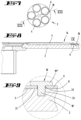
- FIG. 5 is the section according to line V-V on FIG. 4 to illustrate a first exemplary embodiment
- FIG. 6 is a magnified view of the VI cutout on FIG. 5 .
- FIG. 7 is a view according to FIG. 4 .
- FIG. 8 is the section according to line VIII-VIII on FIG. 7 to illustrate a second exemplary embodiment
- FIG. 9 is a magnified view of the IX cutout on FIG. 8 .
- FIG. 10 is a view according to FIG. 4 .
- FIG. 11 is the section according to the XI-XI line on FIG. 10 to illustrate a second exemplary embodiment
- FIG. 12 is a magnified view of the XII cutout on FIG. 11 .
- FIG. 13 is a magnified view of the XIII cutout on FIG. 11 .
- FIG. 14 is a view of an exemplary embodiment in which a lowermost covering plate 6 is adjacent to two substrate holders 4 .
- FIG. 15 is an exemplary embodiment in which a lowermost covering plate 36 partially envelops a substrate holder 4 .
- FIG. 1 schematically depicts a CVD reactor 1 according to the invention with a housing, in which are located a gas inlet organ 27 for letting in process gases, a susceptor 2 for supporting substrates to be coated, and a heating device 29 for heating the susceptor 2 .
- the susceptor 2 rests on a carrier 32 , with which the susceptor 2 can be rotary driven around an axis.
- Covering elements 5 , 15 are located on the susceptor 2 .
- the susceptor arrangement has varyingly designed covering elements 5 , 15 for illustrating different variants of the invention.
- a susceptor arrangement preferably has exclusively covering elements 5 , 15 that are designed identically to each other.
- a covering element 5 consists of two flat bodies designed identically to each other, which consist of solid silicon carbide.
- the lowermost covering plate 16 has an underside that lies directly opposite a broad side 3 of the susceptor 2 consisting of graphite.
- a gap 11 is formed between the downwardly facing broad side surface of the lowermost covering plate 16 and the upwardly facing broad side 3 by a socket 21 or a spacer element 20 .
- the uppermost covering plate 17 is congruent to the lowermost covering plate 16 .
- Both covering plates 16 , 17 form peripheral edges that run on a circular arc line, which border a storage place of a substrate holder 4 .
- the substrate holder 4 is inserted in a pocket 22 having a pocket floor into which undepicted gas lines empty, through which a purging gas can be fed, lifting the substrate holder 4 and rotationally driving it, suspended on a gas cushion.
- a centering pin can be inserted in the center of the floor of the pocket 22 , which engages into a centering opening on the underside of the substrate holder 4 , so as to in this way form a rotational axis around which the substrate holder 4 can rotate when the purging gas is fed into the gap between the floor of the pocket 22 and the underside of the substrate holder 4 .
- the two covering plates 16 , 17 lying one over the other have openings 13 , 19 that align with each other, which in turn align with insertion openings 24 in the broad side 3 of the susceptor 2 .
- a spacer element 20 lies between the lowermost covering plate 16 and broad side 3 or socket 21 , and has an opening through which a shaft 18 ′ of a positioning element 18 reaches.
- the shaft 18 ′ of the positioning element 18 reaches through the two openings 13 , 19 of the two covering plates 16 , 17 lying one over the other.
- a head 18 ′′ having a larger diameter than the shaft 18 ′ lies on the upwardly facing upper side of the uppermost covering plate 17 . It forms a free surface that faces toward the process chamber 28 .
- the positioning element 18 can be fabricated out of silicon carbide.
- a positioning element 18 with a shaft 18 ′ and a head 18 ′′ only reaches through an opening 23 of a lowermost covering plate 6 , so as to connect this lowermost covering plate 6 with the susceptor 2 , while forming a gap 11 between the susceptor broad side 3 and the lowermost covering plate 6 .
- the susceptor 2 has an insertion opening 24 , into which the lower end of the shaft 18 ′ is inserted.
- FIGS. 11 to 13 along with FIGS. 8 to 9 show an exemplary embodiment in which the uppermost covering plate 7 has a smaller surface extension than the lowermost covering plate 6 .
- the stack comprised of two covering plates 6 , 7 be connected with the susceptor with only two positioning elements 8 .
- the opening 23 through which the shaft 8 ′ of the positioning element 8 reaches can have a somewhat larger diameter than the shaft 8 ′ of the positioning element 8 , so that the constituents of the susceptor arrangement can move in relation to each other while heating up the susceptor 2 .
- FIGS. 11 to 13 show the attachment of a roughly triangular uppermost covering plate 7 to a lowermost covering plate 6 .
- the uppermost covering plate 7 lies flatly on the lowermost covering plate 6 .
- the uppermost covering plate 7 has two blind holes 9 , 10 . These are located on the underside of the uppermost covering plate 7 .
- a first blind hole 10 is form fitted to an upper section 8 ′′ of a positioning element 8 that has the shape of a cylinder pin, and whose lower section 8 ′ is inserted into a form fitting opening 13 of the lowermost covering plate 6 .
- the second blind hole 9 in the underside of the uppermost covering plate 7 is designed as an oblong hole, so that the two covering plates 6 , 7 can move in relation to each other given a thermal expansion.
- the lowermost covering plate 6 and the uppermost covering plate 7 are connected with each other with precisely two positioning elements 8 , wherein the positioning elements 8 are arranged one after the other in about a radial direction-relative to the center of rotation of the susceptor 2 .
- the positioning elements 8 it is also possible to arrange the positioning elements 8 one next to the other. For example, they can lie next to each other in an azimuthal direction.
- One end face of the lower section 8 ′ of the positioning element 8 can support itself on the broad side 3 of the susceptor 2 .
- the uppermost covering plate 7 should not be supported on the end face of the upper section 8 ′′ of the positioning element 8 , even if this might also be possible in variants that are not preferred.
- the respective floor of the second blind holes 9 , 10 would support itself on this end face. This would not only make it possible to space the uppermost covering plate 7 apart from the lowermost covering plate 6 by means of a gap.
- the two pin-shaped positioning elements 8 could then also be completely covered by the uppermost covering plate 7 .
- the uppermost covering plate 7 preferably lies on the lowermost covering plate 6 . As a consequence, there is a distance between the end face of the upper section 8 ′′ and the floor of the blind hole 9 , 10 .
- the positioning element 8 consist of silicon carbide.
- the positioning element 8 preferably consists of sapphire, unless it is exposed to the process chamber.
- the two positioning elements 8 with which the lowermost covering plate 6 is fastened to the susceptor 2 define a line, which runs through the two openings 23 of the lowermost covering plate 6 .
- the two positioning elements 8 with which the uppermost covering plate 7 is fastened to the lowermost covering plate 6 likewise define a line.
- the two lines are perpendicular to each other.
- the lowermost covering plate 6 can have an outline contour identical to the lowermost covering plate 16 .
- the lowermost covering plate 6 has two sections, in which the peripheral edge runs on a circular arc line, so that the lowermost covering plate 6 partially envelops two pockets 22 .
- the uppermost covering plate 7 lying on the lowermost covering plate 6 has two edges 30 that meet at an acute angle, which run along a straight line.
- the edges 30 each flank channels 31 , into which fork arms of a fork of a gripping arm can engage, with which a substrate holder 4 can be lifted out of the pocket 22 that stores it.
- FIGS. 2 and 3 further show additional covering plates 25 , 26 , which likewise have rounded edges that flank a pocket 22 .
- FIG. 14 shows a susceptor 2 with five substrate holders 4 arranged thereupon, which are each inserted into a storage pocket.
- the lowermost covering plate 6 is designed in such a way as to have two arced peripheral edges, with which two substrate holders 4 or storage pockets are partially enveloped.
- a storage pocket or a substrate holder 4 arranged therein is partially enveloped by a total of four covering plates, specifically the two radially outer covering plates 6 and two radially inner covering plates 25 .
- a gap forms 33 , at which the two radially outer covering plates 6 adjoin each other.
- FIG. 15 shows an exemplary embodiment for a susceptor 2 in which a substrate holder 4 or the storage pocket that accommodates the substrate holder 4 adjoins three covering plates 36 , 25 .
- a radially outer covering plate 36 has an arc-shaped opening that partially envelops the substrate holder 4 .
- the substrate holder 4 is partially enveloped by precisely one radially outer covering plate 36 .
- the covering plate 36 is a lower covering plate, on which upper covering plates or precisely one upper covering plate can lie.
- an additional, roughly triangular covering plate 34 which adjoins the two covering plates 36 with the formation of a gap 35 .
- the covering plate 34 does not adjoin a substrate holder 4 .
- a susceptor arrangement characterized in that the at least one covering element 5 , 15 comprises a lowermost covering plate 6 , 16 , 36 , which adjoins the first broad side surface 3 of the susceptor 2 , and an uppermost covering plate 7 , 17 , which at least regionally overlaps the lowermost covering plate 6 , 16 , 36 and forms a free broad side surface 14 of the susceptor arrangement.
- a susceptor arrangement characterized in that the two covering plates 6 , 16 , 36 , 7 , 17 consist of SiC, quartz, Al 2 O 3 , ZrO 2 or SiC-coated graphite or some other suitable ceramic, crystalline or amorphous material.
- a susceptor arrangement characterized in that the lowermost covering plate 6 has a larger surface extension than the uppermost covering plate 7 , and the latter lies flatly on the former.
- a susceptor arrangement characterized by storage pockets 22 arranged on the first susceptor broad side 3 for storing the substrate holder 4 , wherein at least one of the lowermost covering plates 6 partially envelops two different storage pockets 22 or one or precisely one storage pocket 22 .
- a susceptor arrangement characterized in that a lowermost covering plate 16 that partially envelops at least two storage pockets 22 and an uppermost covering plate 17 carried by the latter have the same layout.
- a susceptor arrangement characterized by one or several positioning elements 8 , 18 for tying an uppermost covering plate 7 , 17 to a lowermost covering plate 6 , 16 , 36 and/or for tying at least one lowermost covering plate 6 , 16 and an uppermost covering plate 7 , 17 lying thereupon to the susceptor 2 .
- a susceptor arrangement characterized in that the positioning element 18 forms a shaft 18 ′ that can be inserted into an insertion opening 24 of the first susceptor broad side 3 , with it being provided in particular that the shaft 18 ′ reach through an opening of a spacer element 20 , with which the lowermost covering plate 6 , 16 , 36 is positioned at a gap distance to the first susceptor broad side 3 and/or that the positioning element 18 has a head 18 ′′, which has an enlarged diameter in relation to the shaft 18 ′ and lies on the uppermost covering plate 17 or on the lowermost covering plate 16 .
- a susceptor arrangement characterized in that the lowermost covering plate 6 , 16 , 36 has two openings 12 , 13 spaced apart from each other, into which respectively form fitting lower sections 8 ′ of a positioning element 8 engage, whose end face lies on the first susceptor broad side 3 , and that the uppermost covering plate 7 has openings corresponding thereto, of which a first opening 10 is form fitting to an upper section 8 ′′ of the positioning element, and a second opening 9 is designed as an oblong hole, with it being provided in particular that the two openings 9 , 10 of the uppermost covering plate 7 be formed by blind holes.
- a susceptor arrangement characterized in that the uppermost covering plate 7 , 17 directly adjoins the lowermost covering plate 6 , 16 , 36 .
- a CVD reactor characterized in that the at least one covering element 5 , 15 has a lowermost covering plate 6 , 16 , 36 that directly adjoins the first broad side 3 of the susceptor 2 , and an uppermost covering plate 7 , 17 that covers the lowermost covering plate 6 , 16 , 36 and forms a free broad side surface of the susceptor arrangement, in particular according to one of the preceding claims 1 to 9 .
Landscapes
- Chemical & Material Sciences (AREA)
- Chemical Kinetics & Catalysis (AREA)
- Engineering & Computer Science (AREA)
- Materials Engineering (AREA)
- Metallurgy (AREA)
- Organic Chemistry (AREA)
- General Chemical & Material Sciences (AREA)
- Mechanical Engineering (AREA)
- Crystallography & Structural Chemistry (AREA)
- Chemical Vapour Deposition (AREA)
- Container, Conveyance, Adherence, Positioning, Of Wafer (AREA)
Applications Claiming Priority (3)
| Application Number | Priority Date | Filing Date | Title |
|---|---|---|---|
| DE102019105913.5 | 2019-03-08 | ||
| DE102019105913.5A DE102019105913A1 (de) | 2019-03-08 | 2019-03-08 | Suszeptoranordnung eines CVD-Reaktors |
| PCT/EP2020/055308 WO2020182495A1 (de) | 2019-03-08 | 2020-02-28 | Suszeptoranordnung eines cvd-reaktors |
Publications (2)
| Publication Number | Publication Date |
|---|---|
| US20220186374A1 US20220186374A1 (en) | 2022-06-16 |
| US12110591B2 true US12110591B2 (en) | 2024-10-08 |
Family
ID=69780155
Family Applications (1)
| Application Number | Title | Priority Date | Filing Date |
|---|---|---|---|
| US17/593,081 Active 2041-02-02 US12110591B2 (en) | 2019-03-08 | 2020-02-28 | Susceptor arrangement of a CVD reactor |
Country Status (7)
| Country | Link |
|---|---|
| US (1) | US12110591B2 (de) |
| EP (1) | EP3935201A1 (de) |
| JP (1) | JP7539401B2 (de) |
| KR (1) | KR102871297B1 (de) |
| DE (1) | DE102019105913A1 (de) |
| TW (1) | TWI858027B (de) |
| WO (1) | WO2020182495A1 (de) |
Families Citing this family (4)
| Publication number | Priority date | Publication date | Assignee | Title |
|---|---|---|---|---|
| DE102018114208A1 (de) | 2018-06-14 | 2019-12-19 | Aixtron Se | Abdeckplatte zur Abdeckung der zur Prozesskammer weisenden Seite eines Suszeptors einer Vorrichtung zum Abscheiden von SiC-Schichten |
| DE102019114249A1 (de) * | 2018-06-19 | 2019-12-19 | Aixtron Se | Anordnung zum Messen der Oberflächentemperatur eines Suszeptors in einem CVD-Reaktor |
| DE102020123326A1 (de) | 2020-09-07 | 2022-03-10 | Aixtron Se | CVD-Reaktor mit temperierbarem Gaseinlassbereich |
| CN118147594A (zh) * | 2022-12-06 | 2024-06-07 | 中微半导体设备(上海)股份有限公司 | 半导体处理设备及其晶圆托盘组件 |
Citations (14)
| Publication number | Priority date | Publication date | Assignee | Title |
|---|---|---|---|---|
| JPH05267277A (ja) | 1992-03-23 | 1993-10-15 | Hitachi Electron Eng Co Ltd | プラズマcvd装置 |
| DE10323085A1 (de) | 2003-05-22 | 2004-12-09 | Aixtron Ag | CVD-Beschichtungsvorrichtung |
| JP2005142529A (ja) | 2003-10-16 | 2005-06-02 | Tokyo Electron Ltd | 成膜装置 |
| EP1657744A2 (de) | 2004-11-16 | 2006-05-17 | Sumitomo Electric Industries, Ltd. | Halleiterscheiben-Führung, MOCVD Vorrichtung und Aufwachs-Methode für Nitrid-Halbleiter |
| US20060201427A1 (en) | 2000-09-01 | 2006-09-14 | Holger Jurgensen | CVD coating device |
| JP2012178488A (ja) | 2011-02-28 | 2012-09-13 | Taiyo Nippon Sanso Corp | サセプタカバー、該サセプタカバーを備えた気相成長装置 |
| JP2013004593A (ja) | 2011-06-14 | 2013-01-07 | Sharp Corp | 基板支持装置及び気相成長装置 |
| DE102014104218A1 (de) | 2014-03-26 | 2015-10-01 | Aixtron Se | CVD-Reaktor mit Vorlaufzonen-Temperaturregelung |
| US20150345016A1 (en) | 2014-06-02 | 2015-12-03 | Epistar Corporation | Susceptor |
| JP2016035080A (ja) | 2014-08-01 | 2016-03-17 | 大陽日酸株式会社 | サセプタカバーおよび該サセプタカバーを備えた気相成長装置 |
| US20170352575A1 (en) * | 2016-06-07 | 2017-12-07 | Applied Materials, Inc. | Contour Pocket And Hybrid Susceptor For Wafer Uniformity |
| WO2018138197A1 (de) | 2017-01-27 | 2018-08-02 | Aixtron Se | Transportring |
| US20210238740A1 (en) * | 2018-06-06 | 2021-08-05 | Aixtron Se | Cvd reactor with carrying ring for substrate handling, and use of a carrying ring on a cvd reactor |
| US20210262087A1 (en) * | 2018-06-19 | 2021-08-26 | Aixtron Se | Arrangement for measuring the surface temperature of a susceptor in a cvd reactor |
Family Cites Families (2)
| Publication number | Priority date | Publication date | Assignee | Title |
|---|---|---|---|---|
| DE102005055252A1 (de) * | 2005-11-19 | 2007-05-24 | Aixtron Ag | CVD-Reaktor mit gleitgelagerten Suszeptorhalter |
| DE102006018514A1 (de) * | 2006-04-21 | 2007-10-25 | Aixtron Ag | Vorrichtung und Verfahren zur Steuerung der Oberflächentemperatur eines Substrates in einer Prozesskammer |
-
2019
- 2019-03-08 DE DE102019105913.5A patent/DE102019105913A1/de active Pending
-
2020
- 2020-02-28 KR KR1020217032115A patent/KR102871297B1/ko active Active
- 2020-02-28 US US17/593,081 patent/US12110591B2/en active Active
- 2020-02-28 JP JP2021553376A patent/JP7539401B2/ja active Active
- 2020-02-28 EP EP20710074.4A patent/EP3935201A1/de active Pending
- 2020-02-28 WO PCT/EP2020/055308 patent/WO2020182495A1/de not_active Ceased
- 2020-03-04 TW TW109107000A patent/TWI858027B/zh active
Patent Citations (16)
| Publication number | Priority date | Publication date | Assignee | Title |
|---|---|---|---|---|
| JPH05267277A (ja) | 1992-03-23 | 1993-10-15 | Hitachi Electron Eng Co Ltd | プラズマcvd装置 |
| US20060201427A1 (en) | 2000-09-01 | 2006-09-14 | Holger Jurgensen | CVD coating device |
| DE10323085A1 (de) | 2003-05-22 | 2004-12-09 | Aixtron Ag | CVD-Beschichtungsvorrichtung |
| US20060112881A1 (en) * | 2003-05-22 | 2006-06-01 | Johannes Kaeppeler | CVD coating device |
| JP2005142529A (ja) | 2003-10-16 | 2005-06-02 | Tokyo Electron Ltd | 成膜装置 |
| EP1657744A2 (de) | 2004-11-16 | 2006-05-17 | Sumitomo Electric Industries, Ltd. | Halleiterscheiben-Führung, MOCVD Vorrichtung und Aufwachs-Methode für Nitrid-Halbleiter |
| US20060102081A1 (en) | 2004-11-16 | 2006-05-18 | Sumitomo Electric Industries, Ltd. | Wafer Guide, MOCVD Equipment, and Nitride Semiconductor Growth Method |
| JP2012178488A (ja) | 2011-02-28 | 2012-09-13 | Taiyo Nippon Sanso Corp | サセプタカバー、該サセプタカバーを備えた気相成長装置 |
| JP2013004593A (ja) | 2011-06-14 | 2013-01-07 | Sharp Corp | 基板支持装置及び気相成長装置 |
| DE102014104218A1 (de) | 2014-03-26 | 2015-10-01 | Aixtron Se | CVD-Reaktor mit Vorlaufzonen-Temperaturregelung |
| US20150345016A1 (en) | 2014-06-02 | 2015-12-03 | Epistar Corporation | Susceptor |
| JP2016035080A (ja) | 2014-08-01 | 2016-03-17 | 大陽日酸株式会社 | サセプタカバーおよび該サセプタカバーを備えた気相成長装置 |
| US20170352575A1 (en) * | 2016-06-07 | 2017-12-07 | Applied Materials, Inc. | Contour Pocket And Hybrid Susceptor For Wafer Uniformity |
| WO2018138197A1 (de) | 2017-01-27 | 2018-08-02 | Aixtron Se | Transportring |
| US20210238740A1 (en) * | 2018-06-06 | 2021-08-05 | Aixtron Se | Cvd reactor with carrying ring for substrate handling, and use of a carrying ring on a cvd reactor |
| US20210262087A1 (en) * | 2018-06-19 | 2021-08-26 | Aixtron Se | Arrangement for measuring the surface temperature of a susceptor in a cvd reactor |
Non-Patent Citations (3)
| Title |
|---|
| International Preliminary Report on Patentability issued Aug. 25, 2021, from The International Bureau of WIPO, for International Patent Application No. PCT/EP2020/055308 (filed Feb. 28, 2020), with English translation, 26 pgs. |
| International Search Report mailed Aug. 20, 2020, from the ISA/EP, for International Patent Application No. PCT/EP2020/055308 (filed Feb. 28, 2020), 8 pgs. |
| Written Opinion mailed Aug. 20, 2020, from the ISA/EP, for International Patent Application No. PCT/EP2020/055308 (filed Feb. 28, 2020), 24 pgs. |
Also Published As
| Publication number | Publication date |
|---|---|
| DE102019105913A1 (de) | 2020-09-10 |
| TWI858027B (zh) | 2024-10-11 |
| JP7539401B2 (ja) | 2024-08-23 |
| KR20210149728A (ko) | 2021-12-09 |
| EP3935201A1 (de) | 2022-01-12 |
| US20220186374A1 (en) | 2022-06-16 |
| JP2022523594A (ja) | 2022-04-25 |
| TW202039904A (zh) | 2020-11-01 |
| KR102871297B1 (ko) | 2025-10-14 |
| WO2020182495A1 (de) | 2020-09-17 |
Similar Documents
| Publication | Publication Date | Title |
|---|---|---|
| US20220186374A1 (en) | Susceptor arrangement of a cvd reactor | |
| US8535445B2 (en) | Enhanced wafer carrier | |
| US8562746B2 (en) | Sectional wafer carrier | |
| US20130065403A1 (en) | Wafer carrier with thermal features | |
| US7699934B2 (en) | Epitaxial wafer production apparatus and susceptor structure | |
| EP0308946B1 (de) | Chemischer Dampfabscheidungsapparat für die Herstellung von hochqualitativen epitaktischen Schichten mit gleichmässiger Dichte | |
| JP5562409B2 (ja) | 半導体装置の製造方法及び基板製造方法及び基板処理装置 | |
| US20140290564A1 (en) | Susceptor, vapor phase growth apparatus, and method of manufacturing epitaxial wafer | |
| US10793949B2 (en) | Substrate processing apparatus and substrate processing method using the same | |
| JP5195176B2 (ja) | 成膜装置 | |
| CN103283014A (zh) | 薄膜蒸镀装置以及包含此的基板处理系统 | |
| US20110056434A1 (en) | Heat treatment apparatus | |
| EP2397575A1 (de) | Cvd-vorrichtung | |
| US12180590B2 (en) | Cover plate for covering the susceptor side facing the process chamber of a device for depositing SiC layers | |
| CN107958864A (zh) | 基板处理装置及基板处理方法 | |
| JP2011205059A (ja) | 半導体装置の製造方法及び基板製造方法及び基板処理装置 | |
| TW201929050A (zh) | 磊晶成長裝置及使用此裝置的半導體磊晶晶圓的製造方法 | |
| US20100327415A1 (en) | Silicon epitaxial wafer and manufacturing method thereof | |
| WO2004055874A1 (ja) | シリコンエピタキシャルウェーハの製造方法 | |
| JP7604848B2 (ja) | 炭化珪素半導体ウェハの製造装置 | |
| JP7619019B2 (ja) | サセプタ、cvd装置 | |
| JP4515227B2 (ja) | 気相成長装置 | |
| TW202411464A (zh) | 具有支撐環或用於基板之支撐環的cvd反應器 | |
| JP2007005581A (ja) | 基板処理装置 | |
| JP2014063958A (ja) | 基板処理装置 |
Legal Events
| Date | Code | Title | Description |
|---|---|---|---|
| FEPP | Fee payment procedure |
Free format text: ENTITY STATUS SET TO UNDISCOUNTED (ORIGINAL EVENT CODE: BIG.); ENTITY STATUS OF PATENT OWNER: LARGE ENTITY |
|
| AS | Assignment |
Owner name: AIXTRON SE, GERMANY Free format text: ASSIGNMENT OF ASSIGNORS INTEREST;ASSIGNORS:RUDA Y WITT, FRANCISCO;KOLLBERG, MARCEL;RAUF, HENDRIK;SIGNING DATES FROM 20211013 TO 20211028;REEL/FRAME:058018/0752 |
|
| STPP | Information on status: patent application and granting procedure in general |
Free format text: DOCKETED NEW CASE - READY FOR EXAMINATION |
|
| STPP | Information on status: patent application and granting procedure in general |
Free format text: NON FINAL ACTION MAILED |
|
| STPP | Information on status: patent application and granting procedure in general |
Free format text: RESPONSE TO NON-FINAL OFFICE ACTION ENTERED AND FORWARDED TO EXAMINER |
|
| STPP | Information on status: patent application and granting procedure in general |
Free format text: FINAL REJECTION MAILED |
|
| STPP | Information on status: patent application and granting procedure in general |
Free format text: RESPONSE AFTER FINAL ACTION FORWARDED TO EXAMINER |
|
| STPP | Information on status: patent application and granting procedure in general |
Free format text: NOTICE OF ALLOWANCE MAILED -- APPLICATION RECEIVED IN OFFICE OF PUBLICATIONS |
|
| ZAAB | Notice of allowance mailed |
Free format text: ORIGINAL CODE: MN/=. |
|
| STPP | Information on status: patent application and granting procedure in general |
Free format text: PUBLICATIONS -- ISSUE FEE PAYMENT VERIFIED |
|
| STCF | Information on status: patent grant |
Free format text: PATENTED CASE |