US12094662B2 - Electrolytic capacitor and method for producing the same - Google Patents
Electrolytic capacitor and method for producing the same Download PDFInfo
- Publication number
- US12094662B2 US12094662B2 US17/298,438 US201917298438A US12094662B2 US 12094662 B2 US12094662 B2 US 12094662B2 US 201917298438 A US201917298438 A US 201917298438A US 12094662 B2 US12094662 B2 US 12094662B2
- Authority
- US
- United States
- Prior art keywords
- face
- anode
- outer package
- anode lead
- lead terminal
- Prior art date
- Legal status (The legal status is an assumption and is not a legal conclusion. Google has not performed a legal analysis and makes no representation as to the accuracy of the status listed.)
- Active, expires
Links
- 239000003990 capacitor Substances 0.000 title claims abstract description 158
- 238000004519 manufacturing process Methods 0.000 title claims description 18
- 238000002513 implantation Methods 0.000 claims abstract description 20
- 238000005452 bending Methods 0.000 claims description 24
- 238000000034 method Methods 0.000 claims description 16
- 230000000630 rising effect Effects 0.000 claims description 12
- 238000007789 sealing Methods 0.000 claims description 11
- 239000000463 material Substances 0.000 description 21
- 239000007784 solid electrolyte Substances 0.000 description 18
- 229910052751 metal Inorganic materials 0.000 description 17
- 239000002184 metal Substances 0.000 description 17
- 229920001940 conductive polymer Polymers 0.000 description 13
- 239000000853 adhesive Substances 0.000 description 11
- 230000001070 adhesive effect Effects 0.000 description 11
- 239000002923 metal particle Substances 0.000 description 11
- OKTJSMMVPCPJKN-UHFFFAOYSA-N Carbon Chemical compound [C] OKTJSMMVPCPJKN-UHFFFAOYSA-N 0.000 description 10
- 238000003466 welding Methods 0.000 description 10
- 229910052799 carbon Inorganic materials 0.000 description 9
- 239000002245 particle Substances 0.000 description 9
- 229920005989 resin Polymers 0.000 description 9
- 239000011347 resin Substances 0.000 description 9
- 239000000758 substrate Substances 0.000 description 9
- 229920000123 polythiophene Polymers 0.000 description 7
- 229920001187 thermosetting polymer Polymers 0.000 description 7
- 230000015572 biosynthetic process Effects 0.000 description 6
- 230000001771 impaired effect Effects 0.000 description 6
- 229920000128 polypyrrole Polymers 0.000 description 6
- 238000002360 preparation method Methods 0.000 description 6
- 239000000243 solution Substances 0.000 description 6
- 229920000767 polyaniline Polymers 0.000 description 5
- NBIIXXVUZAFLBC-UHFFFAOYSA-N Phosphoric acid Chemical compound OP(O)(O)=O NBIIXXVUZAFLBC-UHFFFAOYSA-N 0.000 description 4
- 239000000178 monomer Substances 0.000 description 4
- 229920000414 polyfuran Polymers 0.000 description 4
- 238000006116 polymerization reaction Methods 0.000 description 4
- -1 polyphenylene Polymers 0.000 description 4
- 239000000126 substance Substances 0.000 description 4
- QTBSBXVTEAMEQO-UHFFFAOYSA-N Acetic acid Chemical compound CC(O)=O QTBSBXVTEAMEQO-UHFFFAOYSA-N 0.000 description 3
- RYGMFSIKBFXOCR-UHFFFAOYSA-N Copper Chemical compound [Cu] RYGMFSIKBFXOCR-UHFFFAOYSA-N 0.000 description 3
- 238000006243 chemical reaction Methods 0.000 description 3
- 229910052802 copper Inorganic materials 0.000 description 3
- 239000010949 copper Substances 0.000 description 3
- 238000013461 design Methods 0.000 description 3
- 238000009413 insulation Methods 0.000 description 3
- 229910044991 metal oxide Inorganic materials 0.000 description 3
- 150000004706 metal oxides Chemical class 0.000 description 3
- 239000000203 mixture Substances 0.000 description 3
- 238000000465 moulding Methods 0.000 description 3
- 230000009467 reduction Effects 0.000 description 3
- 150000003839 salts Chemical class 0.000 description 3
- 238000005245 sintering Methods 0.000 description 3
- 229910000679 solder Inorganic materials 0.000 description 3
- IJGRMHOSHXDMSA-UHFFFAOYSA-N Atomic nitrogen Chemical compound N#N IJGRMHOSHXDMSA-UHFFFAOYSA-N 0.000 description 2
- AFVFQIVMOAPDHO-UHFFFAOYSA-N Methanesulfonic acid Chemical compound CS(O)(=O)=O AFVFQIVMOAPDHO-UHFFFAOYSA-N 0.000 description 2
- BQCADISMDOOEFD-UHFFFAOYSA-N Silver Chemical compound [Ag] BQCADISMDOOEFD-UHFFFAOYSA-N 0.000 description 2
- QAOWNCQODCNURD-UHFFFAOYSA-N Sulfuric acid Chemical compound OS(O)(=O)=O QAOWNCQODCNURD-UHFFFAOYSA-N 0.000 description 2
- 229910045601 alloy Inorganic materials 0.000 description 2
- 239000000956 alloy Substances 0.000 description 2
- 230000004075 alteration Effects 0.000 description 2
- 229910000147 aluminium phosphate Inorganic materials 0.000 description 2
- 238000000748 compression moulding Methods 0.000 description 2
- 238000010586 diagram Methods 0.000 description 2
- 239000006185 dispersion Substances 0.000 description 2
- 239000002019 doping agent Substances 0.000 description 2
- 239000008151 electrolyte solution Substances 0.000 description 2
- 239000000945 filler Substances 0.000 description 2
- 238000010438 heat treatment Methods 0.000 description 2
- 239000007788 liquid Substances 0.000 description 2
- 238000012986 modification Methods 0.000 description 2
- 230000004048 modification Effects 0.000 description 2
- XTEGVFVZDVNBPF-UHFFFAOYSA-N naphthalene-1,5-disulfonic acid Chemical compound C1=CC=C2C(S(=O)(=O)O)=CC=CC2=C1S(O)(=O)=O XTEGVFVZDVNBPF-UHFFFAOYSA-N 0.000 description 2
- 239000010955 niobium Substances 0.000 description 2
- 229910052755 nonmetal Inorganic materials 0.000 description 2
- 229920000642 polymer Polymers 0.000 description 2
- 239000000843 powder Substances 0.000 description 2
- 238000000926 separation method Methods 0.000 description 2
- 229910052709 silver Inorganic materials 0.000 description 2
- 239000004332 silver Substances 0.000 description 2
- 239000010936 titanium Substances 0.000 description 2
- 238000001721 transfer moulding Methods 0.000 description 2
- 229940015297 1-octanesulfonic acid Drugs 0.000 description 1
- YZBGUDOBFPDWKS-UHFFFAOYSA-N 2-[4-(trifluoromethoxy)anilino]benzoic acid Chemical compound OC(=O)C1=CC=CC=C1NC1=CC=C(OC(F)(F)F)C=C1 YZBGUDOBFPDWKS-UHFFFAOYSA-N 0.000 description 1
- BMRVLXHIZWDOOK-UHFFFAOYSA-N 2-butylnaphthalene-1-sulfonic acid Chemical compound C1=CC=CC2=C(S(O)(=O)=O)C(CCCC)=CC=C21 BMRVLXHIZWDOOK-UHFFFAOYSA-N 0.000 description 1
- OORBHYFTTSLSRU-UHFFFAOYSA-N 2-methyl-5-propan-2-ylbenzenesulfonic acid Chemical compound CC(C)C1=CC=C(C)C(S(O)(=O)=O)=C1 OORBHYFTTSLSRU-UHFFFAOYSA-N 0.000 description 1
- RSEBUVRVKCANEP-UHFFFAOYSA-N 2-pyrroline Chemical class C1CC=CN1 RSEBUVRVKCANEP-UHFFFAOYSA-N 0.000 description 1
- BRIXOPDYGQCZFO-UHFFFAOYSA-N 4-ethylphenylsulfonic acid Chemical compound CCC1=CC=C(S(O)(=O)=O)C=C1 BRIXOPDYGQCZFO-UHFFFAOYSA-N 0.000 description 1
- ZDTXQHVBLWYPHS-UHFFFAOYSA-N 4-nitrotoluene-2-sulfonic acid Chemical compound CC1=CC=C([N+]([O-])=O)C=C1S(O)(=O)=O ZDTXQHVBLWYPHS-UHFFFAOYSA-N 0.000 description 1
- MSOTUIWEAQEETA-UHFFFAOYSA-N 4-octylbenzenesulfonic acid Chemical compound CCCCCCCCC1=CC=C(S(O)(=O)=O)C=C1 MSOTUIWEAQEETA-UHFFFAOYSA-N 0.000 description 1
- HWTDMFJYBAURQR-UHFFFAOYSA-N 80-82-0 Chemical compound OS(=O)(=O)C1=CC=CC=C1[N+]([O-])=O HWTDMFJYBAURQR-UHFFFAOYSA-N 0.000 description 1
- ONMOULMPIIOVTQ-UHFFFAOYSA-N 98-47-5 Chemical compound OS(=O)(=O)C1=CC=CC([N+]([O-])=O)=C1 ONMOULMPIIOVTQ-UHFFFAOYSA-N 0.000 description 1
- 229920003026 Acene Polymers 0.000 description 1
- 229910000838 Al alloy Inorganic materials 0.000 description 1
- 238000012935 Averaging Methods 0.000 description 1
- ZOXJGFHDIHLPTG-UHFFFAOYSA-N Boron Chemical compound [B] ZOXJGFHDIHLPTG-UHFFFAOYSA-N 0.000 description 1
- BVKZGUZCCUSVTD-UHFFFAOYSA-L Carbonate Chemical compound [O-]C([O-])=O BVKZGUZCCUSVTD-UHFFFAOYSA-L 0.000 description 1
- ROSDSFDQCJNGOL-UHFFFAOYSA-N Dimethylamine Chemical class CNC ROSDSFDQCJNGOL-UHFFFAOYSA-N 0.000 description 1
- 241000234435 Lilium Species 0.000 description 1
- 239000004640 Melamine resin Substances 0.000 description 1
- 229920000877 Melamine resin Polymers 0.000 description 1
- BAVYZALUXZFZLV-UHFFFAOYSA-N Methylamine Chemical class NC BAVYZALUXZFZLV-UHFFFAOYSA-N 0.000 description 1
- GRYLNZFGIOXLOG-UHFFFAOYSA-N Nitric acid Chemical compound O[N+]([O-])=O GRYLNZFGIOXLOG-UHFFFAOYSA-N 0.000 description 1
- 229920001609 Poly(3,4-ethylenedioxythiophene) Polymers 0.000 description 1
- 229920001665 Poly-4-vinylphenol Polymers 0.000 description 1
- 239000004642 Polyimide Substances 0.000 description 1
- 229920000265 Polyparaphenylene Polymers 0.000 description 1
- XUIMIQQOPSSXEZ-UHFFFAOYSA-N Silicon Chemical compound [Si] XUIMIQQOPSSXEZ-UHFFFAOYSA-N 0.000 description 1
- RTAQQCXQSZGOHL-UHFFFAOYSA-N Titanium Chemical compound [Ti] RTAQQCXQSZGOHL-UHFFFAOYSA-N 0.000 description 1
- 229920001807 Urea-formaldehyde Polymers 0.000 description 1
- 239000002253 acid Substances 0.000 description 1
- 229920000180 alkyd Polymers 0.000 description 1
- HSFWRNGVRCDJHI-UHFFFAOYSA-N alpha-acetylene Natural products C#C HSFWRNGVRCDJHI-UHFFFAOYSA-N 0.000 description 1
- 229910052782 aluminium Inorganic materials 0.000 description 1
- XAGFODPZIPBFFR-UHFFFAOYSA-N aluminium Chemical compound [Al] XAGFODPZIPBFFR-UHFFFAOYSA-N 0.000 description 1
- 150000003863 ammonium salts Chemical class 0.000 description 1
- 238000002048 anodisation reaction Methods 0.000 description 1
- 238000013459 approach Methods 0.000 description 1
- QVGXLLKOCUKJST-UHFFFAOYSA-N atomic oxygen Chemical compound [O] QVGXLLKOCUKJST-UHFFFAOYSA-N 0.000 description 1
- 230000008901 benefit Effects 0.000 description 1
- SRSXLGNVWSONIS-UHFFFAOYSA-N benzenesulfonic acid Chemical compound OS(=O)(=O)C1=CC=CC=C1 SRSXLGNVWSONIS-UHFFFAOYSA-N 0.000 description 1
- 229940092714 benzenesulfonic acid Drugs 0.000 description 1
- MVIOINXPSFUJEN-UHFFFAOYSA-N benzenesulfonic acid;hydrate Chemical compound O.OS(=O)(=O)C1=CC=CC=C1 MVIOINXPSFUJEN-UHFFFAOYSA-N 0.000 description 1
- 239000011230 binding agent Substances 0.000 description 1
- 229910052796 boron Inorganic materials 0.000 description 1
- QDHFHIQKOVNCNC-UHFFFAOYSA-N butane-1-sulfonic acid Chemical compound CCCCS(O)(=O)=O QDHFHIQKOVNCNC-UHFFFAOYSA-N 0.000 description 1
- 239000003575 carbonaceous material Substances 0.000 description 1
- 150000001875 compounds Chemical class 0.000 description 1
- 239000004020 conductor Substances 0.000 description 1
- 229920001577 copolymer Polymers 0.000 description 1
- 230000008878 coupling Effects 0.000 description 1
- 238000010168 coupling process Methods 0.000 description 1
- 238000005859 coupling reaction Methods 0.000 description 1
- 230000001419 dependent effect Effects 0.000 description 1
- 239000002612 dispersion medium Substances 0.000 description 1
- 230000000694 effects Effects 0.000 description 1
- 238000010292 electrical insulation Methods 0.000 description 1
- 238000005868 electrolysis reaction Methods 0.000 description 1
- 239000003792 electrolyte Substances 0.000 description 1
- 239000003822 epoxy resin Substances 0.000 description 1
- 125000005678 ethenylene group Chemical group [H]C([*:1])=C([H])[*:2] 0.000 description 1
- 229910002804 graphite Inorganic materials 0.000 description 1
- 239000010439 graphite Substances 0.000 description 1
- FYAQQULBLMNGAH-UHFFFAOYSA-N hexane-1-sulfonic acid Chemical compound CCCCCCS(O)(=O)=O FYAQQULBLMNGAH-UHFFFAOYSA-N 0.000 description 1
- 230000006872 improvement Effects 0.000 description 1
- 239000011810 insulating material Substances 0.000 description 1
- 238000005304 joining Methods 0.000 description 1
- 229910003002 lithium salt Inorganic materials 0.000 description 1
- 159000000002 lithium salts Chemical class 0.000 description 1
- 150000002697 manganese compounds Chemical class 0.000 description 1
- 229910001092 metal group alloy Inorganic materials 0.000 description 1
- 150000002739 metals Chemical class 0.000 description 1
- 229940098779 methanesulfonic acid Drugs 0.000 description 1
- WUOSYUHCXLQPQJ-UHFFFAOYSA-N n-(3-chlorophenyl)-n-methylacetamide Chemical compound CC(=O)N(C)C1=CC=CC(Cl)=C1 WUOSYUHCXLQPQJ-UHFFFAOYSA-N 0.000 description 1
- PSZYNBSKGUBXEH-UHFFFAOYSA-N naphthalene-1-sulfonic acid Chemical compound C1=CC=C2C(S(=O)(=O)O)=CC=CC2=C1 PSZYNBSKGUBXEH-UHFFFAOYSA-N 0.000 description 1
- FITZJYAVATZPMJ-UHFFFAOYSA-N naphthalene-2,6-disulfonic acid Chemical compound C1=C(S(O)(=O)=O)C=CC2=CC(S(=O)(=O)O)=CC=C21 FITZJYAVATZPMJ-UHFFFAOYSA-N 0.000 description 1
- VILFVXYKHXVYAB-UHFFFAOYSA-N naphthalene-2,7-disulfonic acid Chemical compound C1=CC(S(O)(=O)=O)=CC2=CC(S(=O)(=O)O)=CC=C21 VILFVXYKHXVYAB-UHFFFAOYSA-N 0.000 description 1
- KVBGVZZKJNLNJU-UHFFFAOYSA-N naphthalene-2-sulfonic acid Chemical compound C1=CC=CC2=CC(S(=O)(=O)O)=CC=C21 KVBGVZZKJNLNJU-UHFFFAOYSA-N 0.000 description 1
- 229910052758 niobium Inorganic materials 0.000 description 1
- GUCVJGMIXFAOAE-UHFFFAOYSA-N niobium atom Chemical compound [Nb] GUCVJGMIXFAOAE-UHFFFAOYSA-N 0.000 description 1
- 229910017604 nitric acid Inorganic materials 0.000 description 1
- 229910052757 nitrogen Inorganic materials 0.000 description 1
- WLGDAKIJYPIYLR-UHFFFAOYSA-N octane-1-sulfonic acid Chemical compound CCCCCCCCS(O)(=O)=O WLGDAKIJYPIYLR-UHFFFAOYSA-N 0.000 description 1
- 230000008520 organization Effects 0.000 description 1
- 229910052760 oxygen Inorganic materials 0.000 description 1
- 239000001301 oxygen Substances 0.000 description 1
- 239000005011 phenolic resin Substances 0.000 description 1
- 229920003227 poly(N-vinyl carbazole) Polymers 0.000 description 1
- 229920000172 poly(styrenesulfonic acid) Polymers 0.000 description 1
- 229920001197 polyacetylene Polymers 0.000 description 1
- 229920000647 polyepoxide Polymers 0.000 description 1
- 229920002098 polyfluorene Polymers 0.000 description 1
- 229920001721 polyimide Polymers 0.000 description 1
- 230000000379 polymerizing effect Effects 0.000 description 1
- 229940005642 polystyrene sulfonic acid Drugs 0.000 description 1
- 239000004814 polyurethane Substances 0.000 description 1
- 229920002635 polyurethane Polymers 0.000 description 1
- XAEFZNCEHLXOMS-UHFFFAOYSA-M potassium benzoate Chemical compound [K+].[O-]C(=O)C1=CC=CC=C1 XAEFZNCEHLXOMS-UHFFFAOYSA-M 0.000 description 1
- 238000003825 pressing Methods 0.000 description 1
- 238000004080 punching Methods 0.000 description 1
- 239000002994 raw material Substances 0.000 description 1
- 229910052710 silicon Inorganic materials 0.000 description 1
- 239000010703 silicon Substances 0.000 description 1
- 229920002050 silicone resin Polymers 0.000 description 1
- 159000000000 sodium salts Chemical class 0.000 description 1
- 238000005476 soldering Methods 0.000 description 1
- 230000001502 supplementing effect Effects 0.000 description 1
- 229910052715 tantalum Inorganic materials 0.000 description 1
- GUVRBAGPIYLISA-UHFFFAOYSA-N tantalum atom Chemical compound [Ta] GUVRBAGPIYLISA-UHFFFAOYSA-N 0.000 description 1
- 229910052719 titanium Inorganic materials 0.000 description 1
- ITMCEJHCFYSIIV-UHFFFAOYSA-N triflic acid Chemical compound OS(=O)(=O)C(F)(F)F ITMCEJHCFYSIIV-UHFFFAOYSA-N 0.000 description 1
- GETQZCLCWQTVFV-UHFFFAOYSA-N trimethylamine Chemical class CN(C)C GETQZCLCWQTVFV-UHFFFAOYSA-N 0.000 description 1
- 229920006305 unsaturated polyester Polymers 0.000 description 1
- 229910052720 vanadium Inorganic materials 0.000 description 1
- GPPXJZIENCGNKB-UHFFFAOYSA-N vanadium Chemical compound [V]#[V] GPPXJZIENCGNKB-UHFFFAOYSA-N 0.000 description 1
Images


Classifications
-
- H—ELECTRICITY
- H01—ELECTRIC ELEMENTS
- H01G—CAPACITORS; CAPACITORS, RECTIFIERS, DETECTORS, SWITCHING DEVICES, LIGHT-SENSITIVE OR TEMPERATURE-SENSITIVE DEVICES OF THE ELECTROLYTIC TYPE
- H01G9/00—Electrolytic capacitors, rectifiers, detectors, switching devices, light-sensitive or temperature-sensitive devices; Processes of their manufacture
- H01G9/004—Details
- H01G9/008—Terminals
- H01G9/012—Terminals specially adapted for solid capacitors
-
- H—ELECTRICITY
- H01—ELECTRIC ELEMENTS
- H01G—CAPACITORS; CAPACITORS, RECTIFIERS, DETECTORS, SWITCHING DEVICES, LIGHT-SENSITIVE OR TEMPERATURE-SENSITIVE DEVICES OF THE ELECTROLYTIC TYPE
- H01G9/00—Electrolytic capacitors, rectifiers, detectors, switching devices, light-sensitive or temperature-sensitive devices; Processes of their manufacture
- H01G9/004—Details
- H01G9/08—Housing; Encapsulation
-
- H—ELECTRICITY
- H01—ELECTRIC ELEMENTS
- H01G—CAPACITORS; CAPACITORS, RECTIFIERS, DETECTORS, SWITCHING DEVICES, LIGHT-SENSITIVE OR TEMPERATURE-SENSITIVE DEVICES OF THE ELECTROLYTIC TYPE
- H01G9/00—Electrolytic capacitors, rectifiers, detectors, switching devices, light-sensitive or temperature-sensitive devices; Processes of their manufacture
- H01G9/15—Solid electrolytic capacitors
Definitions
- the present invention relates to an electrolytic capacitor and a method for producing the same.
- Electrolytic capacitors have a small equivalent series resistance (ESR) and excellent frequency characteristics, and therefore are mounted in various electronic devices.
- An electrolytic capacitor includes a capacitor element including an anode section and a cathode section, an anode lead terminal electrically connected to the anode section, and a cathode lead terminal electrically connected to the cathode section.
- the capacitor element is usually sealed by an outer package.
- the capacitor element is sealed, for example, by accommodating the capacitor element and materials (an uncured thermosetting resin and a filler) of the outer package in a mold, and performing transfer molding, compression molding, or the like. At this time, side faces of the outer package are designed in a tapered shape, taking into account the releasability of the mold (see PTL 1).
- electrolytic capacitors are required to have a higher capacity and a smaller size.
- side faces of an outer package with a rectangular parallelepiped shape for example, is formed in a tapered shape, the volume of the outer package becomes smaller than that of an outer package with a rectangular parallelepiped shaped, and therefore the size of the capacitor element that can be sealed by the outer package also becomes smaller.
- a first aspect of the present invention relates to an electrolytic capacitor including: a capacitor element including an anode section and a cathode section; an anode lead terminal electrically connected to the anode section; a cathode lead terminal electrically connected to the cathode section; and an outer package that covers the capacitor element, wherein the anode section includes an anode body, and an anode wire extending outwardly of the anode body from an implantation face of the anode body, the outer package has a first face opposing the implantation face, and a second face and a third face sharing one side with the first face and opposing each other, the first face, the second face, and the third face each include a planar portion, an area of the second face is larger than an area of the third face, an angle ⁇ 1 formed between the planar portion of the first face and the planar portion of the second face is less than 90 degrees, and the first face includes a protruding portion located on an extension of the anode wire, and protrud
- a second aspect of the present invention relates to a method for producing an electrolytic capacitor, including: a preparation step of preparing a capacitor element to which an anode lead terminal and a cathode lead terminal are connected; a sealing step of forming an outer package that seals the capacitor element, a portion of the anode lead terminal, and a portion of the cathode lead terminal; and a bending step of bending an exposed portion of the anode lead terminal that is exposed from the outer package, wherein a first face of the outer package formed in the sealing step includes a protruding portion protruding to an outside of the outer package, and, in the bending step, the exposed portion of the anode lead terminal is bent using a roller that moves along the protruding portion.
- FIG. 1 is a cross-sectional view schematically showing an outer package according to an embodiment of the present invention.
- FIG. 2 is a perspective view schematically showing an external appearance of the outer package according to an embodiment of the present invention.
- FIG. 3 is a cross-sectional view of the outer package of FIG. 2 taken along the line A-A.
- FIG. 4 is an enlarged cross-sectional view of relevant parts of the outer package of FIG. 2 taken along the line A-A.
- FIG. 5 is a perspective view schematically showing an electrolytic capacitor according to an embodiment of the present invention.
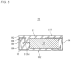
- FIG. 6 is a cross-sectional view of the electrolytic capacitor of FIG. 5 taken along the line B-B.
- FIG. 7 is a perspective view schematically showing an electrolytic capacitor according to another embodiment of the present invention.
- FIG. 8 is a cross-sectional view of the electrolytic capacitor of FIG. 7 taken along the line C-C.
- FIG. 9 A is a perspective view schematically showing an electrolytic capacitor according to another embodiment of the present invention.
- FIG. 9 B is a cross-sectional view of the electrolytic capacitor of FIG. 9 A taken along the line X 1 -X 2 .
- FIG. 10 A is a perspective view showing how an anode lead terminal and a cathode lead terminal are connected to a capacitor element in FIG. 9 A , with the illustration of an outer package being omitted.
- FIG. 10 B is a cross-sectional view of the electrolytic capacitor of FIG. 10 A taken along the line Y 1 -Y 2 .
- FIG. 11 is a cross-sectional view schematically showing a capacitor element according to an embodiment of the present invention.
- FIG. 12 is a flowchart illustrating a method for producing an electrolytic capacitor according to an embodiment of the present invention.
- FIG. 13 A is a cross-sectional view schematically showing a capacitor element to which lead terminals prepared in a preparation step of the production method according to an embodiment of the present invention are joined.
- FIG. 13 B is a cross-sectional view schematically showing a mold and a capacitor element accommodated in the mold in a sealing step of the production method according to an embodiment of the present invention.
- FIG. 13 C is a cross-sectional view schematically showing how a first mold is released in the sealing step of the production method according to an embodiment of the present invention.
- FIG. 13 D is a cross-sectional view schematically showing how an anode lead terminal is bent in a bending step of the production method according to an embodiment of the present invention.
- FIG. 14 is a schematic diagram of an anode lead terminal (lead frame) used in production of an electrolytic capacitor according to an embodiment of the present invention.
- FIG. 15 is a cross-sectional view schematically showing a conventional outer package.
- the outer dimensions of an electrolytic capacitor are strictly defined. Accordingly, in order to increase the capacity of an electrolytic capacitor, it is necessary to increase the size of a capacitor element sealed in the electrolytic capacitor, without changing the outer dimensions of the electrolytic capacitor.
- FIG. 15 is a cross-sectional view schematically showing a conventional outer package.
- a capacitor element 210 includes an anode wire 202 electrically connected to an anode body and implanted through one face (implantation face) of the anode body.
- a certain length L 1 is secured between the anode wire 202 and a side face 211 X of the outer package 211 that is located on an extension of the anode wire 202 .
- an anode lead terminal which is not shown, is joined to the anode wire 202 .
- at least a certain length L 2 is also required for the portion where the anode wire 202 is implanted.
- a length L 211 in a longitudinal direction A of the anode wire 202 , of the outer package 211 near the portion where the anode wire 202 is disposed, is shorter at least by the length L 3 than a design value L of the electrolytic capacitor in the longitudinal direction A. That is, the size of the capacitor element 210 needs to be determined taking also into account the reduced length L 3 , in addition to the above-described lengths L 1 and L 2 . Accordingly, the length of the capacitor element 210 in the longitudinal direction A is further reduced relative to the design value L.
- a protruding portion is provided on one face (first face) of the outer package that is located on an extension of the anode wire, thus supplementing at least a portion of the L 3 reduced by tapering. Consequently, the length of the outer package in the longitudinal direction A of the anode wire approaches the design value L. Accordingly, it is possible to increase the length of the capacitor element in the longitudinal direction A, while securing the above-described lengths L 1 and L 2 .
- the protruding portion is provided on the first face, the other portions of the first face maintain the tapered shape, and therefore the releasability of the mold is less likely to be impaired.
- an electrolytic capacitor includes: a capacitor element including an anode section and a cathode section; an anode lead terminal electrically connected to the anode section; a cathode lead terminal electrically connected to the cathode section; and an outer package that covers the capacitor element.
- the anode section includes an anode body, and an anode wire extending outwardly of the anode body from an implantation face of the anode body.
- the outer package has a first face opposing the implantation face, and a second face and a third face sharing one side with the first face and opposing each other. The first face, the second face, and the third face each include a planar portion.
- An area of the second face is larger than an area of the third face.
- An angle ⁇ 1 formed between the planar portion of the first face and the planar portion of the second face is less than 90 degrees.
- the first face includes a protruding portion located on an extension of the anode wire, and protruding to an outside of the outer package.
- the area of the second face is greater than the area of the third face, and is, for example, 102% or more, or 105% or more of the third area.
- the area of the second face may be 120% or less, or 115% or less of the area of the third face. Note that the area in this case does not refer to a surface area, but refers to a projected area as viewed in the normal direction of the second face or the third face (usually, a projected area as viewed from an upper face or a lower face of the electrolytic capacitor).
- the first to third faces of the outer package usually means three of six principal faces of an outer surface of the outer package formed to have a substantially rectangular parallelepiped shape.
- the outer surface of the outer package may also have a fourth face sharing one side with each of the second face and the third face and located opposite to the first face.
- the first to fourth faces usually refer to four principal faces of the substantially rectangular parallelepiped shape except for two faces opposing each other.
- the first to fourth faces each include a planar portion, and the angle formed between two faces of the outer package can be defined from the angles formed between the planar portions.
- the first to fourth faces may include a portion having a curved shape, include some recesses and projections, and/or be formed by a plurality of bent planar faces, as long as they include a planar portion.
- the first to fourth faces may each include a plurality of planar portions. In that case, the angle formed between the faces are defined using one of the plurality of planar portions that has the largest areas.
- the first face of the outer package includes a plurality of planar portions 11 X, 111 x , and 112 (and a planar portion coupling 11 X and 112 ).
- an angle ⁇ 1 formed between the planar portion of the first face and the planar portion of the second face is defined from an angle formed between the planar portion 11 X, which has the largest area, of the first face and the planar portion 11 Y of the second face.
- the angle formed between the first face and the second face is smaller than 90 degrees.
- the angle ⁇ 1 formed between the planar portion of the first face and the planar portion of the second face is not particularly limited as long as it is less than 90 degrees, and can be set as appropriate taking into account the releasability of the mold and the size of a capacitor element that is to be sealed.
- the angle ⁇ 1 may be 89 degree or less, or 88 degree or less, for example.
- the angle ⁇ 1 may be 80 degrees or more, or 83 degrees or more, for example.
- the protruding portion is formed, for example, when assuming a virtual first plane forming an angle ⁇ 2 greater than the angle ⁇ 1 and less than or equal to 90 degrees with the planar portion of the second face and a virtual third plane coplanar with the planar portion of the third face, in a virtual space between the virtual first plane, the virtual third plane, and the planar portion of the actual first face.
- the angle ⁇ 2 is not particularly limited as long as it is greater than the angle ⁇ 1 and less than or equal to 90 degrees.
- the angle ⁇ 2 may be set such that an angle ⁇ 3 formed between the virtual first plane and the virtual third plane is greater than or equal to 90 degrees.
- the angle ⁇ 3 is less than 90 degrees, the releasability of the mold is likely to be impaired.
- the angle ⁇ 2 may be less than 90 degrees, or less than or equal to 89 degrees.
- the angle ⁇ 2 may be greater than 80 degrees, or greater than 83 degrees.
- the electrolytic capacitor according to the present embodiment includes a capacitor element including an anode section and a cathode section, an anode lead terminal electrically connected to the anode section, a cathode lead terminal electrically connected to the cathode section, and an outer package.
- the outer package has a first face, and a second face and a third face sharing one side with the first face and opposing each other. The outer package covers the capacitor element, with a portion of the anode lead terminal and a portion of the cathode lead terminal exposed therefrom.
- the anode lead terminal includes a first anode lead portion along the second face, a second anode lead portion rising from the first anode lead portion and being in contact with the anode section, and a third anode lead portion extending from the first anode lead portion along the first face, further extending along the third face, and exposed from the outer package at least on the third face.
- a first bent portion may be formed at a boundary between the first anode lead portion and the second anode lead portion, and a second bent portion may be formed at a boundary between the first anode lead portion and the third anode lead portion.
- the first bent portion is located on the capacitor element side relative to the second bent portion, as viewed in a direction perpendicular to the planar portion of the second face.
- the first bent portion located on the capacitor element side relative to the second bent portion means that the distance from the first bent portion to the cathode section of the capacitor element is shorter than the distance from the second bent portion to the cathode section of the capacitor element, when the electrolytic capacitor is viewed in a direction perpendicular to the planar portion of the second face.
- the cathode lead terminal is usually disposed along the second face, and includes a first cathode lead portion electrically connected to the cathode section.
- the cathode lead terminal may further include a second cathode lead portion extending from the first cathode lead portion along the fourth face which shares one side with each of the second face and the third face and constitutes an outer face of the outer package opposite to the first face, and further extending along the third face exposed from the outer package at least on the third face.
- the anode or cathode lead terminal extending along the first to fourth faces or the planar portions thereof is not limited to a case where the lead terminal extends parallel to each of the faces, while keeping a predetermined separation distance therefrom, but also includes a case where the lead terminal extends, for example, in a direction inclined from a direction parallel to each of the faces.
- the above expression does not mean that the lead terminal extends along the recesses and projections while being bent.
- a portion of the third anode lead portion that extends along the first face may extend in a direction substantially parallel to the virtual first plane.
- the anode lead terminal may integrally include the first anode lead portion, the second anode lead portion, and the third anode lead portion.
- the anode lead terminal is in the state of being folded and bent, and is connected to the anode section via the second anode lead portion.
- at least a portion of the third anode lead portion is exposed from the outer package. Accordingly, a connection to an external substrate can be established via the third anode lead portion.
- the first anode lead portion is disposed along the second face of the outer package, and the second anode lead portion is folded in a direction toward the anode section from a direction along the second face, and is in contact with the anode section. Accordingly, an electrical connection between the anode lead terminal and the anode section may be established by the second anode lead portion.
- the direction toward the anode section is usually a direction along the first face and/or a direction intersecting the second face, but may be a direction obliquely inclined relative to the first face and the second face.
- a method for connecting the anode section and the anode lead terminal involves making a cut in the anode lead frame, and raising a portion of the anode lead frame so as to be in contact with the anode section (e.g., see Japanese Laid-Open Patent Publication Nos. 2001-126958 and 2015-088718).
- an electrical connection between the anode of the electrolytic capacitor and an external substrate is achieved via the first anode lead portion provided on the second face side, and an electrical connection between the cathode of the electrolytic capacitor and the external substrate is established via the first cathode lead portion also provided on the second face side.
- an outer face of the cathode section on the second face side is connected to the first cathode lead portion in order to electrically connect the cathode section and the first cathode lead portion.
- a thickness of the outer package covering the second face side of the cathode section is small. Therefore, it is difficult to extend the first anode lead portion to the side approaching the cathode section of the second face while ensuring necessary insulation between the first anode lead portion and the cathode section, thus making it difficult to increase the area of the first anode lead portion.
- This problem is pronounced in the case of adopting a method that involves raising a portion of the anode lead frame and using that portion for achieving contact with the anode section, because the area of the first anode lead portion is further reduced by the area of the raised portion.
- the remainder of the anode lead terminal after the second anode lead portion has been raised is folded along the outer surface of the outer package, and the third anode lead portion is disposed on the third face located opposite to the second face.
- the shape and the area of the third anode lead portion disposed on the third face are unconstrained by the second anode lead portion that is brought into contact with the anode section.
- the aforementioned shape and area can be freely set without being constrained by the arrangement, the shape and the size of the cathode section of the capacitor element.
- connection reliability with the external substrate is improved. It is also possible to extend the third anode lead portion along the third face beyond the position of an end of the cathode section on the first face side, as viewed from a direction perpendicular to the second face.
- the second anode lead portion is formed, for example, by making a cut in a portion, other than the first bent portion, of a contour line of a formation region of the second anode lead portion of the anode lead terminal, folding the second anode lead portion using the first bent portion as an axis, and raising the second anode lead portion so as to be erected from the first principal face.
- the anode lead terminal may include, on the second face, a region (opening) in which the anode lead terminal does not extend.
- the anode lead terminal is folded along the first face in the same direction as the second anode lead portion, thus forming a third anode lead portion.
- the third anode lead portion is further folded, at a predetermined position, from the first face along the third face.
- the third region may be a protruding portion protruding outward from the planar portion of the first face.
- the first region of the third anode lead portion can be provided around the protruding portion so as to be exposed from the outer package.
- the third anode lead portion may be exposed from the outer package at least in the second region along the third face. Furthermore, in addition to the second region, the first region along the first face may also be exposed from the outer package. When an electrical connection between the second region and an external substrate is established by soldering, solder can be also attached to the first region, thus making it possible to improve the connection reliability.
- an anode section includes an anode body and an anode wire extending from the anode body, and the anode wire is joined to an anode lead terminal.
- the present invention is not limited thereto.
- FIG. 1 is a cross-sectional view schematically showing an outer package according to the present embodiment. Note, however, that protruding portions have been omitted for the sake of convenience.
- FIG. 1 shows a virtual first plane 11 Xv forming an angle ⁇ 2 greater than an angle ⁇ 1 and less than or equal to 90 degrees with a planar portion 11 Y of a second face of an outer package 11 , and a virtual third plane 11 Zv coplanar with a planar portion 11 Z of a third face.
- the protruding portion is formed, for example, in a virtual space R between the virtual first plane 11 Xv, the planar portion 11 X of an actual first face, and the virtual third plane 11 Zv. However, the protruding portion is provided on an extension of at least an anode section (anode wire 2 ).
- a protruding portion that does not oppose the anode wire 2 may be disposed in the virtual space R.
- the first protruding portion is formed, for example, from the second face side relative to a position in the first face that opposes the anode wire, and at least to the third face side relative to the position opposing the anode wire.
- the first protruding portion may be formed, from a side (first side) of the first face on the second face side or the vicinity of the first side, to the third face side relative to the position opposing the anode wire.
- the outside shape of the outer package, including the first protruding portion is simplified when the outer package is viewed from the second face side, and the releasability of the mold is further less likely to be impaired.
- Such a first protruding portion includes, for example, a protruding face extending toward the virtual third face from the first side or the vicinity of the first side, and a plurality of rising faces connecting the protruding face and the first face.
- an angle ⁇ 4 (see FIG. 4 ) formed between the protruding face and the planar portion of the second face is greater than the angle ⁇ 1 and less than or equal to the angle ⁇ 2 .
- the angle ⁇ 4 may be the same as the angle ⁇ 2 .
- the protruding face is coplanar with the virtual first plane.
- the angle ⁇ 2 and the angle ⁇ 4 may both be 89 degrees to 90 degrees. This can maximize the length (L 11 ) of the outer package in the longitudinal direction A, including the first protruding portion, to the extent that the releasability of the mold is not impaired. Accordingly, it is possible to maximize the length of the capacitor element in the longitudinal direction A.
- the first protruding portion may extend to reach the above-described virtual third plane.
- a length T 1 (see FIG. 4 ) of the first protruding portion in the normal direction of the second face (hereinafter may also be referred to as the thickness direction of the outer package) may be, for example, greater than or equal to 60% and less than or equal to 100%, or greater than or equal to 65% and less than or equal to 80%, of the length T of the outer package in the thickness direction between the second face and the third face.
- An average length W 1 (see FIG. 2 ) of the first protruding portion in a direction along the first side may be shorter than a length W of the first face in the width direction.
- the ratio (W 1 /W) of the length W 1 to the length W may be, for example, 60% or less, or 40% or less.
- W 1 /W may be 10% or more, or 25% or more.
- the length W 1 of the first protruding portion is calculated by averaging the lengths at three arbitrarily selected locations in the width direction when the first protruding portion is viewed in the normal direction of the first face.
- the length W of the first face in the width direction is also calculated in the same manner.
- FIG. 2 is a perspective view schematically showing an external appearance of an outer package according to an embodiment.
- FIG. 3 is a cross-sectional view of the outer package of FIG. 2 taken along the line A-A.
- FIG. 4 is an enlarged cross-sectional view of relevant parts of the outer package of FIG. 2 taken along the line A-A.
- the electrolytic capacitor according to the present embodiment includes a capacitor element 10 including an anode section and a cathode section, an anode lead terminal (not shown) electrically connected to the anode section, a cathode lead terminal (not shown) electrically connected to the cathode section, and an outer package 11 that covers the capacitor element 10 .
- the anode section includes an anode body, and an anode wire 2 extending from an implantation face 1 X of the anode body.
- the outer package 11 has a first face including a planar portion 11 X and opposing the implantation face 1 X, and a second face and a third face sharing one side with the first face and opposing each other.
- the second face and the third face include planar portions 11 Y and 11 Z, respectively.
- the area of the planar portion 11 Y of the second face is about 108% of the area of the planar portion 11 Z of the third face, and the angle ⁇ 1 formed between the planar portion 11 X of the first face and the planar portion 11 Y of the second face is about 87 degrees.
- the anode wire 2 includes a first portion (not shown) embedded into the anode body through the implantation face 1 X, and a second portion 2 b extending from the implantation face 1 X toward the planar portion 11 X of the first face of the outer package 11 .
- a first protruding portion 111 located on an extension of the second portion 2 b of the anode wire, and protruding to the outside of the outer package 11 is formed on the first face.
- the first protruding portion 111 is formed in a virtual space defined by the planar portion 11 X, a virtual first plane 11 Xv, and a virtual third plane 11 Zv.
- An angle ⁇ 2 formed between the virtual first plane 11 Xv and the planar portion 11 Y of the second face is about 89 degrees
- an angle ⁇ 3 formed between the virtual first plane 11 Xv and the virtual third plane 11 Zv is about 91 degrees.
- the first protruding portion 111 includes a protruding face 111 x , and a plurality of rising faces ( 111 y and 111 z ) connecting the protruding face 111 x and the planar portion 11 X.
- the protruding face 111 x extends toward the virtual third face 11 Zv, from a position located on the second face side relative to a position that opposes the second portion 2 b of the anode wire in the vicinity of the first side 11 a of the planar portion 11 X of the first face on the second face (planar portion 11 Y) side, and, to a position to cover a portion of the first face (planar portion 11 X) that intersects an extension of the second portion 2 b of the anode wire.
- the first protruding portion 111 further includes a rising face opposing the rising face 111 y.
- An angle ⁇ 4 formed between the protruding face 111 x and the planar portion 11 Y of the second face is about 89 degrees, and is greater than the angle ⁇ 1 and the same as the angle ⁇ 2 . That is, the protruding face 111 x is coplanar with the virtual first plane 11 Xv.
- the length T 1 of the first protruding portion 111 in the thickness direction of the outer package 11 is about 71% of the length T between the second face 11 Y and the third face 11 Z in the aforementioned thickness direction.
- the ratio (W 1 /W) of the average length W 1 of the first protruding portion 111 in the width direction to the length W of the planar portion 11 X of the first face in the width direction is about 32%.
- the ratio (S 1 /S) of an area S 1 of the first protruding portion 111 to an area S of the entire first face is about 23%.
- the value of the length L 11 of the outer package 11 in the longitudinal direction A on an extension of the second portion 2 b is set to a maximum value to the extent that the releasability of the mold is not impaired. Accordingly, it is possible to increase the length of the capacitor element 10 in the longitudinal direction A to a maximum value, while securing the length L 1 required between the second portion 2 b and the first face of the outer package 11 and the length L 2 of the second portion 2 b required for joining the second portion 2 b and the anode lead terminal.
- first protruding portion 111 is disposed on a portion of the first face, and the other portions of the first face maintain the tapered shape, and therefore the releasability of the mold used when forming the outer package 11 is also less likely to be impaired.
- the outer package 11 shown in FIGS. 2 to 4 includes, in addition to the first protruding portion 111 , a protruding portion (second protruding portion 112 ) other than the first protruding portion.
- the second protruding portion 112 in the illustrated example is formed in a band shape along the above-described first side 11 a .
- Such a second protruding portion 112 contributes to an improvement in the releasability of the mold.
- the anode lead terminal joined to the anode wire may be led out from the first face of the outer package.
- the led-out anode lead terminal is bent, and covers a portion of the third face of the outer package, for example.
- the electrolytic capacitor is mounted in an electronic device, with the third face of the outer package opposing the electronic device.
- the exposed portion of the anode lead terminal led out from the outer package may be bent along the above-described virtual first plane.
- the exposed portion may be bent so as not to overlap the first protruding portion. In this case, it is easier to inhibit the outer dimensions of the electrolytic capacitor from becoming larger than those of the outer package. As a result, the outer package can be made larger, so that the size of the capacitor element can be increased.
- FIG. 5 is a perspective view schematically showing an example of the electrolytic capacitor according to the present embodiment.
- FIG. 6 is a cross-sectional view of the electrolytic capacitor of FIG. 5 taken along the line B-B.
- the electrolytic capacitor shown in FIGS. 5 and 6 includes the outer package shown in FIGS. 2 to 4 .
- the anode lead terminal 13 is led out to the outside of the outer package 11 from the planar portion 11 X of the first face.
- the anode lead terminal 13 led out from the planar portion 11 X is bent along the planar portion 11 Z of the third face of the outer package 11 , after it is bent so that its outwardly facing face (outer face) 13 X extends along the virtual first plane 11 Xv (see FIG. 4 ).
- the portion (exposed portion) of the anode lead terminal 13 that is led out from the outer package 11 does not overlap the first protruding portion 111 . Furthermore, the protruding face and the outer face 13 X of the anode lead terminal are both coplanar with the virtual first plane. Accordingly, the outer dimensions of the electrolytic capacitor 20 are less likely to be larger than those of the outer package 11 . In other words, even when the first protruding portion 111 is formed on the outer package 11 , and the anode lead terminal 13 is disposed around the outer package 11 , it is possible to suppress an increase in the outer dimensions of the electrolytic capacitor 20 . Accordingly, it is possible to increase the size of the capacitor element 10 .
- a cathode lead terminal 14 is also led out to the outside of the outer package 11 from a face of the outer package 11 that opposes the planar portion 11 X of the first face, and is thereafter bent so as to be disposed on the third face.
- the cathode lead terminal 14 is joined to the cathode section of the capacitor element 10 , using, for example, a conductive adhesive material, which is not shown.
- the first protruding portion 111 is disposed at substantially the center, in the width direction, of the planar portion 11 X of the first face of the outer package 11 so as to correspond to the second portion 2 b of the anode wire 2 .
- the anode lead terminal 13 is led out to the outside from two locations of the first face 11 X so as to avoid the first protruding portion 111 . Thereafter, the two band-shaped portions of the anode lead terminal 13 are coupled in a region on the third face 11 Z side on the virtual first face 11 Xv.
- an opening surrounding the peripheries of the rising faces of the first protruding portion 111 may be form in the exposed portion of the anode lead terminal 13 .
- an increase in the outer dimensions of the electrolytic capacitor 20 is suppressed.
- the electrical resistance is reduced, and the joined area of the anode lead terminal 13 and the electronic device, which is not shown, is increased. Accordingly, the connection reliability is improved.
- the shape of the first protruding portion, and the shape and the arrangement of the anode lead terminal are not limited thereto.
- FIG. 7 is a perspective view schematically showing an electrolytic capacitor according to another embodiment.
- FIG. 8 is a cross-sectional view of the electrolytic capacitor of FIG. 7 taken along the like C-C.
- the first protruding portion 111 includes a protruding face 111 x , and a plurality of rising faces ( 111 y and 111 z ) connecting the protruding face 111 x and the planar portion 11 X of the first face.
- the protruding face 111 x is extends from a portion of the first side 11 a in the vicinity of the center of the first side 11 a , and thereafter extends toward the virtual third plane 11 Zv to a position to cover a portion of the first face (planar portion 11 X) that intersects an extension of the second portion 2 b of the anode wire, while the length thereof in the width direction constant is kept constant.
- the outer package 11 does not include the second protruding portion. Except for the foregoing, the outer package shown in FIGS. 7 and 8 has the same configuration as the outer package shown in FIGS. 2 to 4 .
- the anode lead terminal 13 is led out to the outside of the outer package 11 from the second face.
- the anode lead terminal 13 led out from the second face is directly disposed on the second face.
- the anode lead terminal 13 does not overlap the first protruding portion 111 , and therefore the outer dimensions of the electrolytic capacitor 20 is less likely to be larger than those of the outer package 11 . Accordingly, it is possible to increase the size of the capacitor element 10 .
- the cathode lead terminal 14 may also be led out to the outside of the outer package 11 from the second face, and be disposed directly on the second face.
- the cathode lead terminal 14 is joined to the cathode section of the capacitor element 10 , for example, using a conductive adhesive material 8 .
- the conductive adhesive material 8 is, for example, a mixture of a thermosetting resin and carbon particles or metal particles, which will be described later.
- FIG. 9 A is a perspective view schematically showing an electrolytic capacitor 100 according to an embodiment of the present invention.
- FIG. 9 B is a cross-sectional view of the electrolytic capacitor 100 of FIG. 9 A taken along the line X 1 -X 2 .
- FIGS. 10 A and 10 B are diagrams showing how an anode lead terminal 50 and a cathode lead terminal 60 are connected to a capacitor element 10 in FIGS. 9 A and 9 B , respectively, with the illustration of the outer package 70 being omitted.
- FIG. 10 B is a cross-sectional view of the electrolytic capacitor of FIG. 10 A taken along the line Y 1 -Y 2 .
- the electrolytic capacitor 100 includes a capacitor element 10 including an anode section 6 and a cathode section 7 , an anode lead terminal (anode lead frame) 50 electrically connected to the anode section 6 , a cathode lead terminal (cathode lead frame) 60 electrically connected to the cathode section 7 , and an outer package 70 .
- the outer package 70 covers the capacitor element 10 , with a portion of the anode lead terminal 50 and a portion of the cathode lead terminal 60 being exposed.
- the anode section 6 includes an anode body 1 and an anode wire 2 extending from the anode body 1 , and the anode wire 2 is joined to the anode lead terminal 50 .
- the outer surface of the outer package 70 includes a first face A 1 , a second face A 2 sharing one side with the first face A 1 , a third face A 3 sharing one side with the first face A 1 and located opposite to the second face A 2 , and a fourth face A 4 sharing one side with each of the second face A 1 and the third face A 3 .
- the fourth face A 4 is located opposite to the first face A 1 (see FIG. 9 B ).
- the anode lead terminal 50 includes a first anode lead portion 51 , a second anode lead portion 52 , and a third anode lead portion 53 .
- the third anode lead portion 53 further includes a first region 53 a extending in a direction along the first face A 1 (more specifically, a direction along the virtual first plane), and a second region 53 b bent from the first region 53 a so as to extend along the third face A 3 (see FIGS. 10 A, 10 B ).
- the anode lead terminal 50 is folded from the first face A 1 at a first bent portion B 1 and a second bent portion B 2 .
- a portion of the anode lead frame 50 is folded at the first bent portion B 1 in a direction toward the anode wire 2 , and constitutes the second anode lead portion 52 .
- Another portion of the anode lead terminal 50 is folded along the first face A 1 at the second bent portion B 2 , and constitutes the third anode lead portion 53 .
- the remainder of the anode lead frame 50 that extends along the second face A 2 constitutes the first anode lead portion 51 .
- the second anode lead portion 52 is connected to the anode wire 2 .
- the whole of the third anode lead portion 53 is exposed from the outer package 70 , and the third anode lead portion 53 extends from the second bent portion B 2 along the first face A 1 so as to cover the first face A 1 in the first region 53 a , and is thereafter folded in the vicinity of a boundary between the first face A 1 and the third face A 3 toward a direction along the third face A 3 , and extends along the third face A 3 so as to cover the third face A 3 in the second region 53 b.
- the first bent portion B 1 is located on the capacitor element 10 side relative to the second bent portion B 2 . That is, the second anode lead portion 52 is folded at a position closer to the cathode section of the capacitor element than the third anode lead portion 53 is. Due to this, the anode lead terminal 50 has an opening formed on the first face side as shown in FIG. 10 A .
- the first region 53 a exposed from the outer package 70 does not cover the entire surface of the first face, and a region in which the anode lead terminal 50 (third anode lead portion 53 ) is not exposed is present in a region (third region) on the first face that corresponds to the above-described opening.
- a protruding portion (first protruding portion) 71 is provided in a region on the first face that corresponds to the above-described opening, and the first region 53 a extends so as to surround the protruding portion 71 .
- the anode wire 2 extends toward the protruding portion 71 (see FIG. 10 A ; however, the protruding portion 71 is not shown in FIG. 10 A ).
- the cathode lead terminal 60 includes a first cathode lead portion 61 and a second cathode lead portion 62 .
- a portion of the cathode lead terminal 60 is folded from the second face A 2 along the fourth face A 4 , and the folded portion constitutes the first cathode lead portion 61 , and the remainder constitutes the second cathode lead portion 62 .
- the first cathode lead portion 61 is electrically connected to the cathode section of the capacitor element 10 via a conductive adhesive (e.g., silver paste), which is not shown, on the second face A 2 side.
- a conductive adhesive e.g., silver paste
- the second cathode lead portion 62 further includes a first region 62 a extending in a direction along the fourth face A 4 , and a second region 62 b bent from the first region 62 a so as to extend along the third face A 3 . As shown in FIG. 10 B , the whole of the second cathode lead portion 62 , including the first region 62 a and the second region 62 b , is exposed from the outer package 70 .
- the cathode lead terminal 60 similarly to the anode lead terminal 50 , the cathode lead terminal 60 also has an opening formed on the fourth face A 4 side.
- the first region 62 a of the cathode lead terminal 60 exposed from the outer package 70 does not cover the entire surface of the fourth face A 4 , and a region in which the cathode lead terminal 60 (second cathode lead portion 62 ) is not exposed is present in a region on the fourth face that corresponds to the above-described opening.
- a protruding portion 72 is provided in the region on the fourth face that corresponds to the above-described opening, and the first region 62 a is formed so as to surround the protruding portion 72 .
- the distance from the second face A 2 on which an electrical connection between the cathode lead terminal 60 and the cathode section is established, to the capacitor element 10 i.e., the thickness of the outer package that covers the second face A 2 side of the cathode section
- the distance from the third face A 3 of the outer package to the capacitor element 10 i.e., the thickness of the outer package that coves the third face A 3 side of the cathode section.
- the area of the first anode lead portion 51 is reduced as a result of providing the second anode lead portion 52 . Consequently, the area of the first anode lead portion 51 is limited by the arrangement of the second anode lead portion and the cathode section, and it is therefore necessary to take measures to increase the land area for connection to an external substrate.
- an electrical connection between the electrolytic capacitor and an external substrate is established on the third face A 3 , which is located opposite to the second face A 2 on which an electrical connection between the cathode lead terminal 60 and the cathode section is established. Therefore, the shape and the area of the third anode lead portion 53 are not dependent on the arrangement of the cathode section, and can be set freely. As shown in FIG. 10 B , it is possible that an end position L 3 of the third anode lead portion 53 is set at a position to overlap the cathode section beyond L 2 . Accordingly, it is possible to increase the area of the third anode lead portion 53 without causing a capacity decrease, and also improve the connection reliability with the external substrate.
- a capacitor element according to the present embodiment will be described in detail, taking, as an example, a case where a solid electrolyte layer is included as an electrolyte.
- FIG. 11 is a cross-sectional view schematically showing an example of the capacitor element according to the present embodiments.
- a capacitor element 10 includes an anode section 6 and a cathode section 7 .
- the anode section 6 includes an anode body 1 including a dielectric layer 3 , and an anode wire 2 .
- the cathode section 7 includes a solid electrolyte layer 4 formed on the dielectric layer 3 , and a cathode layer 5 (a carbon layer 5 a and a metal paste layer 5 b ) that covers the surface of the solid electrolyte layer 4 .
- the anode wire 2 has a first portion 2 a embedded into the anode body 1 through one face (implantation face) of the anode body 1 , and a second portion 2 b extending from the aforementioned one face of the anode body 1 .
- the anode section includes, for example, an anode body, and an anode wire extending from one face of the anode body and electrically connected to an anode lead terminal.
- the anode body is a rectangular parallelepiped-shaped porous sintered body obtained by sintering metal particles.
- a valve metal such as titanium (Ti), tantalum (Ta), or niobium (Nb) are used.
- the anode body one or more kinds of metal particles are used.
- the metal particles may be an alloy made of two or more metals.
- an alloy containing a valve metal, silicon, vanadium, boron, and the like can be used.
- a compound containing a valve metal and a typical element such as nitrogen may be used.
- the valve metal alloy is mainly composed of a valve metal, and contains, for example, 50 atom % or more of a valve metal.
- the anode wire is formed of a conductive material.
- the material of the anode wire is not particularly limited, and examples thereof include copper, aluminum, and an aluminum alloy, in addition to the above-described valve metal.
- the materials that form the anode body and the anode wire may be of the same kind or different kinds.
- the cross-sectional shape of the anode wire is not particularly limited, and examples thereof include a circular shape, a track shape (a shape formed by straight lines parallel to each other, and two curved lines connecting ends of the straight lines), an oval shape, a rectangular shape, and a polygonal shape.
- a dielectric layer is formed on the surface of the anode body.
- the dielectric layer is formed of a metal oxide, for example.
- Examples of the method for forming a layer containing a metal oxide on the surface of the anode body include a method involving immersing the anode body in a chemical conversion solution to anodize the surface of the anode body, and a method involving heating the anode body under an atmosphere containing oxygen.
- the dielectric layer is not limited to the above-described layer containing a metal oxide, as long as it is insulating.
- the cathode section includes a solid electrolyte layer formed on the dielectric layer, and a cathode layer that covers the solid electrolyte layer.
- the solid electrolyte layer may be formed so as to cover at least a portion of the dielectric layer.
- a manganese compound or a conductive polymer is used, for example.
- the conductive polymer include polypyrrole, polythiophene, polyfuran, polyaniline, polyacetylene, polyphenylene, polyparaphenylene vinylene, polyacene, polythiophene vinylene, polyfluorene, polyvinyl carbazole, polyvinyl phenol, polypyridine, or derivatives of these polymers. These may be used alone or in a combination of two or more.
- the conductive polymer may be a copolymer of two or more monomers. Because of the excellent conductivity, polythiophene, polyaniline, or polypyrrole may be used. In particular, polypyrrole may be used because of the excellent repellency.
- the solid electrolyte layer containing the above-described conductive polymer is formed, for example, by polymerizing a raw material monomer on the dielectric layer. Alternatively, the solid electrolyte layer is formed by applying a liquid containing the above-described conductive polymer to the dielectric layer.
- the solid electrolyte layer is formed by one or more solid electrolyte layers. When the solid electrolyte layer is formed by two or more layers, the compositions and the formation methods (polymerization methods) of the conductive polymers used for the layers may be different.
- polypyrrole, polythiophene, polyfuran, polyaniline, and the like mean polymers including polypyrrole, polythiophene, polyfuran, polyaniline, and the like, respectively, as basic skeletons thereof. Accordingly, polypyrrole, polythiophene, polyfuran, polyaniline and the like may include derivatives thereof.
- polythiophene includes poly(3,4-ethylenedioxythiophene).
- various dopants may be added to a polymerization liquid for forming the conductive polymer, a solution or a dispersion of the conductive polymer.
- the dopants include, but are not particularly limited to, 1,5-naphthalenedisulfonic acid, 1,6-naphthalenedisulfonic acid, 1-octanesulfonic acid, 1-naphthalenesulfonic acid, 2-naphthalenesulfonic acid, 2,6-naphthalenedisulfonic acid, 2,7-naphthalenedisulfonic acid, 2-methyl-5-isopropylbenzenesulfonic acid, 4-octylbenzenesulfonic acid, 4-nitrotoluene-2-sulfonic acid, m-nitrobenzenesulfonic acid, n-octylsulfonic acid, n-butanesulfonic acid, n-hexanesulfonic acid, o-
- the derivatives include metal salts such as a lithium salt, a potassium salt, and a sodium salt, ammonium salts such as a methyl ammonium salt, a dimethyl ammonium salt, and a trimethyl ammonium salt, a piperidium salt, a pyrrolidium salt, and a pyrrolinium salt.
- metal salts such as a lithium salt, a potassium salt, and a sodium salt
- ammonium salts such as a methyl ammonium salt, a dimethyl ammonium salt, and a trimethyl ammonium salt
- a piperidium salt such as a pyrrolidium salt, and a pyrrolinium salt.
- an average particle size D50 of the particles is, for example, greater than or equal to 0.01 ⁇ m and less than or equal to 0.5 ⁇ m.
- the average particle size D50 of the particles is in this range, the particles can easily penetrate into the anode body.
- the cathode layer includes, for example, a carbon layer formed so as to cover the solid electrolyte layer, and a metal paste layer formed on the surface of the carbon layer.
- the carbon layer contains a conductive carbon material such as graphite, and a resin.
- the metal paste layer contains, for example, metal particles (e.g., silver) and a resin. Note that the configuration of the cathode layer is not limited to this configuration. The configuration of the cathode layer may be any configuration including a current collecting function.
- One end of the anode lead terminal is joined to the anode wire using a conductive adhesive material or solder, or by resistance welding or laser welding.
- the other end of the anode lead terminal is led out from the outer package to the outside.
- a part of the exposed portion of the anode lead terminal is disposed on one of the faces of the outer package, together with the cathode lead terminal.
- the material of the anode lead terminal is not particularly limited as long as it is electrochemically and chemically stable, and is conductive.
- the anode lead terminal may be a metal such as copper, or may be a nonmetal.
- the shape of the anode lead terminal is not particularly limited as long as it is plate-shaped. In terms of height reduction, the thickness of the anode lead terminal (the length between the principal faces of the anode lead terminal) may be greater than or equal to 25 ⁇ m and less than or equal to 200 ⁇ m, or may be 25 ⁇ m and less than or equal to 100 ⁇ m.
- the anode lead terminal may be joined to the anode wire using a conductive adhesive material or solder, or may be joined to the anode wire by resistance welding or laser welding.
- the conductive adhesive material is, for example, a mixture of a thermosetting resin and carbon particles or metal particles, which will be described later.
- the cathode lead terminal is joined to the cathode layer via a conductive adhesive material, for example.
- One end of the cathode lead terminal is disposed inside the outer package.
- the other end of the cathode lead terminal is led out from the outer package to the outside.
- a part of the exposed portion of the cathode lead terminal is disposed on one of the faces of the outer package, together with the anode lead terminal.
- the material of the cathode lead terminal is not particularly limited as long as it is electrochemically and chemically stable, and is conductive.
- the cathode lead terminal may be a metal such as copper, or may be a nonmetal.
- the shape of the cathode lead terminal is also not particularly limited, and is long and plate-shaped, for example. In terms of height reduction, the thickness of the cathode lead terminal may be greater than or equal to 25 ⁇ m and less than or equal to 200 ⁇ m, or may be greater than or equal to 25 ⁇ m and less than or equal to 100 ⁇ m.
- the outer package is provided in order to provide electrical insulation between the anode lead terminal and the cathode lead terminal, and is formed of an insulating material (outer package material).
- the outer package material contains a thermosetting resin, for example.
- the thermosetting resin include an epoxy resin, a phenol resin, a silicone resin, a melamine resin, a urea resin, an alkyd resin, a polyurethane, a polyimide, and an unsaturated polyester.
- the outer package includes a second face and a third face sharing one side with the first face and opposing each other, the area of the second face is larger than the area of the third face, the first face, the second face, and the third face each include a planar portion, and the angle ⁇ 1 formed between the planar portion of the first face and the planar portion of the second face is less than 90 degrees.
- the first protruding portion is formed in a virtual space R defined by the planar portion of the first face, a virtual first plane sharing a first side of the first face on the second face side with the first face and forming an angle ⁇ 2 greater than the angle ⁇ 1 and less than or equal to 90 degrees with the planar portion of the second face, and a virtual third plane coplanar with the planar portion of the third face.
- the first protruding portion includes a protruding face, and a plurality of rising faces connecting the protruding face and the first face, and the protruding face is coplanar with the virtual first face.
- the production method according to the present embodiment is useful for a case such as the one described above where the outside shape of the outer package is tapered, and the outer package includes the first protruding portion.
- a capacitor element is prepared.
- Valve metal particles and an anode wire are placed in a mold such that a first portion is embedded in the valve metal particles, and the whole is pressure molded, followed by sintering in a vacuum, to produce an anode section in which the first portion is embedded into a porous sintered body through one face of the porous sintered body.
- the pressure applied during pressure molding is not particularly limited, and is about 10 N or more and 100 N or less, for example.
- the valve metal particles may be mixed with a binder such as polyacrylic carbonate as needed.
- a dielectric layer is formed on the anode body.
- the anode body is immersed in a chemical conversion tank filled with an aqueous electrolytic solution (e.g., an aqueous phosphoric acid solution), a second portion of the anode wire is connected to the anode body placed in the chemical conversion tank, and anodization is performed, whereby a dielectric layer made of an oxide film of the valve metal can be formed on the surface of the anode body.
- the aqueous electrolytic solution is not limited to an aqueous phosphoric acid solution, and it is possible to use nitric acid, acetic acid, or sulfuric acid, for example.
- a solid electrolyte layer is formed.
- a step of forming a solid electrolyte layer containing a conductive polymer is described.
- the solid electrolyte layer containing a conductive polymer is formed on at least a portion of the dielectric layer, for example, by a method in which the anode body with the dielectric layer formed thereon is impregnated with a monomer or an oligomer, and thereafter the monomer or the oligomer is polymerized by chemical polymerization or electrolysis polymerization, or a method in which the anode body with the dielectric layer formed thereon is impregnated with a solution or a dispersion of a conductive polymer, and dried.
- a cathode layer composed of a carbon layer and a metal paste layer is formed.
- the configuration of the cathode layer is not limited thereto as long as the configuration includes a current collecting function.
- an anode lead terminal and a cathode lead terminal are prepared, and joined to the capacitor element.
- a bent portion (internal bent portion) that is to be disposed inside the outer package is formed on the anode lead terminal.
- the internal bent portion is formed, for example, by pressing or the like.
- the position of the internal bent portion of the anode lead terminal is set as appropriate according to the length, the diameter, and the like of the anode wire.
- An internal bent portion may also be formed on the cathode lead terminal.
- the anode lead terminal and the cathode lead terminal are disposed at predetermined positions. At this time, a conductive adhesive material is applied to a predetermined position of the cathode layer.
- the capacitor element is placed on the lead terminals disposed at the predetermined positions. Then, the second portion of the anode wire and the vicinity of one end of the anode lead terminal are joined by laser welding, resistance welding, or the like. At this time, the vicinity of the one end of the cathode lead terminal is joined to the cathode layer via the conductive adhesive material.
- FIG. 13 A is a cross-sectional view schematically showing a capacitor element to which the lead terminals prepared in the preparation step of the production method according to the present embodiment are joined.
- a capacitor element 10 includes an anode wire 2 implanted through an implantation face 1 X.
- An anode lead terminal 13 is joined to the anode wire 2 (second portion 2 b ).
- a cathode lead terminal 14 is joined to a cathode section of the capacitor element 10 .
- a bent portion corresponding to the internal bent portion is formed on the anode lead terminal 13 .
- the capacitor element and materials (e.g., an uncured thermosetting resin and a filler) of the outer package are accommodated in a mold, and the capacitor element is sealed by transfer molding, compression molding, or the like. At this time, a portion of the anode lead terminal and a portion of the cathode lead terminal are led out from the mold.
- the molding conditions are not particularly limited, and the time and temperature conditions may be set as appropriate taking into account the curing temperature or the like of the thermosetting resin.
- FIG. 13 B is a cross-sectional view schematically showing a mold and a capacitor element accommodated in the mold in a sealing step of the production method according to the present embodiment.
- a capacitor element 10 is accommodated in a mold 30 , together with a material 11 P of an outer package.
- a portion of an anode lead terminal 13 and a portion of a cathode lead terminal 14 are led out from the mold 30 .
- the mold 30 includes a deep first mold 31 capable of accommodating the capacitor element 10 , and a second mold 32 including a shallow stepped portion.
- a recess 31 a for forming a first protruding portion is formed in the first mold 31 .
- the bottom face of the first mold 31 has a smaller area than the area of the opening of the first mold 31 , and the first mold 31 has a tapered shape.
- a container-shaped mold 30 is formed by fitting the first mold 31 and the second mold 32 to each other.
- the anode lead terminal 13 and the cathode lead terminal 14 are led out to the outside from gaps formed when the first mold 31 and the second mold 32 are fitted to each other.
- the capacitor element covered by the outer package is removed from the mold.
- This provides an electrolytic capacitor including a capacitor element, an anode lead terminal, a cathode lead terminal, and an outer package that covers the capacitor element and a portion of each of the lead terminals.
- FIG. 13 C is a cross-sectional view schematically showing how the first mold is released in the sealing step of the production method according to the present embodiment.
- the portion of the anode lead terminal and the portion of the cathode lead terminal that are exposed from the mold are folded, to form respective external bent portions of the lead terminals Consequently, a portion of the anode lead terminal and a portion of the cathode lead terminal are disposed on the third face of the outer package.
- the anode lead terminal is bent along the virtual first plane (see FIG. 4 ).
- the first protruding portion formed on a side face of the outer package may be used as a guide.
- a bending roller is moved from the second face toward the third face of the outer package while being pressed against the first protruding portion, thus bending the anode lead terminal.
- the bending roller is stably moved, and therefore the accuracy of the bending is increased.
- FIG. 13 D is a cross-sectional view schematically showing how the anode lead terminal is bent in the bending step of the production method according to the present embodiment.
- a bending roller 40 is moved from the second face (planar portion 11 Y) toward the third face (planar portion 11 Z) of the outer package 11 while being guided by the first protruding portion 111 .
- the anode lead terminal 13 is pressed by the bending roller 40 and bent into a shape conforming to the virtual first plane. Consequently, the protruding face of the first protruding portion 111 and the outer face 13 X of the anode lead terminal 13 are both coplanar with the virtual first plane 11 Xv.
- the anode lead terminal 13 is further bent along the third face.
- the cathode lead terminal 14 may also be bent using a bending roller.
- the anode lead terminal (anode lead frame) 50 shown in FIG. 14 may be used. Accordingly, the electrolytic capacitor 100 shown in FIG. 9 A may be produced.
- a U-shaped cut C (the portion indicated by the dashed line in FIG. 14 ) is formed along a contour line of a formation region (e.g., a rectangular region) of the second anode lead portion 52 , except for one straight side of the contour line. Punching of the anode lead terminal 50 and the formation of the cut may be performed simultaneously.
- the portion in which no cut is formed constitutes the first bent portion B 1 .
- the dashed dotted line in FIG. 14 is a portion serving as an axis for folding.
- a length U of the cut may be any length longer than the height of the anode wire 2 from the second face A 2 .
- a through hole 54 may be formed adjacent to the cut of the anode lead terminal 50 , such that in the sealing step and the bending step, the anode lead terminal (third anode lead portion) is disposed around the first protruding portion of the outer package, and that the anode lead terminal does not cover the first protruding portion.
- the formation region of the second anode lead portion 52 is folded using the first bent portion B 1 as an axis, thus erecting the second anode lead portion 52 from the anode lead frame.
- the bent portion is formed, for example, by bending or the like.
- the position of the first bent portion B 1 may be set as appropriate according to the size or the like (in particular, the position of the portion of the capacitor element from which the anode wire 2 is extended) of the capacitor element.
- the anode lead terminal 50 is bent from a direction along the second face A 2 to a direction along the first face A 1 , and further bent from the direction along the first face A 1 to a direction along the third face A 3 , which opposes the second face A 2 .
- the cathode lead terminal is bent from a direction along the second face A 2 to a direction along the fourth face A 4 , and further bent from the direction along the fourth face A 4 to a direction along the third face A 3 , which opposes the second face A 2 .
- a boundary between a portion along the first face A 1 and a portion along the second face A 2 is the second bent portion B 2 .
- a portion of the anode lead terminal 50 that extends in a direction away from the outer package 70 with respect to the second bent portion B 2 constitutes the third anode lead portion 53 .
- a portion other than the second anode lead portion 52 constitutes the first anode lead portion 51 .
- a portion of the cathode lead terminal 60 that extends in a direction away from the outer package 70 with respect to a boundary between a portion along the first face A 1 and a portion along the fourth face A 4 constitutes the second cathode lead portion 62 , and the remainder constitutes the first cathode lead portion 61 .
- the electrolytic capacitor according to the present invention allows the size of a capacitor element to be increased, and therefore can be used in a variety of applications.
Landscapes
- Engineering & Computer Science (AREA)
- Power Engineering (AREA)
- Microelectronics & Electronic Packaging (AREA)
- Fixed Capacitors And Capacitor Manufacturing Machines (AREA)
- Chemical & Material Sciences (AREA)
- Chemical Kinetics & Catalysis (AREA)
- Electrochemistry (AREA)
- Manufacturing & Machinery (AREA)
- Electric Double-Layer Capacitors Or The Like (AREA)
Abstract
Description
-
- 20, 100 . . . Electrolytic capacitor
- 10 . . . Capacitor element
- 1 . . . Anode body
- 1 x . . . Implantation face
- 2 . . . Anode wire
- 2 a . . . First portion
- 2 b . . . Second portion
- 3 . . . Dielectric layer
- 4 . . . Solid electrolyte layer
- 5 . . . Cathode layer
- 5 a . . . Carbon layer
- 5 b . . . Metal paste layer
- 6 . . . Anode section
- 7 . . . Cathode section
- 8 . . . Conductive adhesive material
- 11, 70 . . . Outer package
- A1 . . . First face
- A2 . . . Second face
- A3 . . . Third face
- A4 . . . Fourth face
- 11X . . . First face (planar portion)
- 11Y . . . Second face (planar portion)
- 11Z . . . Third face (planar portion)
- 11Xv . . . Virtual first plane
- 11Zv . . . Virtual third plane
- 11 a . . . First side
- 111 . . . First protruding portion
- 111 x . . . Protruding face
- 111 y, 111 z . . . Rising face
- 112 . . . Second protruding portion
- 11P . . . Material of outer package
- 71, 72 . . . Protruding portion
- 13, 50 . . . Anode lead terminal
- 13X . . . Outer face
- 51 . . . First anode lead portion
- 52 . . . Second anode lead portion
- 53 . . . Third anode lead portion
- 53 a . . . First region
- 53 b . . . Second region
- B1 . . . First bent portion
- B2 . . . Second bent portion
- 14, 60 . . . Cathode lead terminal
- 61 . . . First cathode lead portion
- 62 . . . Second cathode lead portion
- 62 a . . . First region
- 62 b . . . Second region
- 30 . . . Mold
- 31 . . . First mold
- 31 a . . . Recess
- 32 . . . Second mold
- 40 . . . Bending roller
- 210 . . . Capacitor element
- 202 . . . Anode wire
- 211 . . . Outer package
- 211X . . . Side face
Claims (11)
Applications Claiming Priority (5)
| Application Number | Priority Date | Filing Date | Title |
|---|---|---|---|
| JP2018-225595 | 2018-11-30 | ||
| JP2018225595 | 2018-11-30 | ||
| JP2018225594 | 2018-11-30 | ||
| JP2018-225594 | 2018-11-30 | ||
| PCT/JP2019/046924 WO2020111278A1 (en) | 2018-11-30 | 2019-11-29 | Electrolytic capacitor and method of manufacturing same |
Publications (2)
| Publication Number | Publication Date |
|---|---|
| US20220028622A1 US20220028622A1 (en) | 2022-01-27 |
| US12094662B2 true US12094662B2 (en) | 2024-09-17 |
Family
ID=70852808
Family Applications (1)
| Application Number | Title | Priority Date | Filing Date |
|---|---|---|---|
| US17/298,438 Active 2041-01-11 US12094662B2 (en) | 2018-11-30 | 2019-11-29 | Electrolytic capacitor and method for producing the same |
Country Status (3)
| Country | Link |
|---|---|
| US (1) | US12094662B2 (en) |
| JP (1) | JP7496517B2 (en) |
| WO (1) | WO2020111278A1 (en) |
Families Citing this family (1)
| Publication number | Priority date | Publication date | Assignee | Title |
|---|---|---|---|---|
| JP7813930B1 (en) | 2025-03-14 | 2026-02-13 | ニチコン株式会社 | Manufacturing method for stacked solid electrolytic capacitors |
Citations (20)
| Publication number | Priority date | Publication date | Assignee | Title |
|---|---|---|---|---|
| JPS59131144U (en) | 1983-02-22 | 1984-09-03 | 日本電気株式会社 | Chip type solid electrolytic capacitor |
| JPS60220922A (en) * | 1985-04-01 | 1985-11-05 | 日立エーアイシー株式会社 | Chip type capacitor |
| JPS6151752U (en) * | 1984-09-10 | 1986-04-07 | ||
| JPH01230218A (en) * | 1988-03-10 | 1989-09-13 | Matsuo Denki Kk | How to treat solid electrolytic capacitor terminals |
| JPH0361324U (en) | 1989-10-17 | 1991-06-17 | ||
| JPH03212920A (en) * | 1990-01-18 | 1991-09-18 | Elna Co Ltd | Solid state electrolyte capacitor and its unit |
| JPH0722289A (en) * | 1993-07-01 | 1995-01-24 | Hitachi Aic Inc | Solid electrolytic capacitor |
| JPH0722280A (en) | 1993-06-16 | 1995-01-24 | Showa Denko Kk | Chip solid electrolytic capacitor |
| US5387762A (en) * | 1992-12-28 | 1995-02-07 | Rohm Co., Ltd. | Resin-packaged electronic component having bent lead terminals |
| JPH0846109A (en) * | 1994-07-29 | 1996-02-16 | Nec Kyushu Ltd | Lead forming die |
| US5554823A (en) * | 1991-12-27 | 1996-09-10 | Rohm Co., Ltd. | Packaging device and its manufacturing method |
| JPH0992575A (en) | 1995-07-18 | 1997-04-04 | Nec Toyama Ltd | Chip-type solid-state electrolytic capacitor |
| JPH10149953A (en) | 1996-11-19 | 1998-06-02 | Nec Corp | Chip type electronic components |
| JPH11288844A (en) | 1998-04-03 | 1999-10-19 | Matsuo Electric Co Ltd | Resin-sealed electronic component and method of manufacturing the same |
| US20010028544A1 (en) | 2000-04-07 | 2001-10-11 | Nec Corporation | Chip capacitor, a fabrication method for the same, and a metal mold |
| US20040094322A1 (en) * | 2001-04-13 | 2004-05-20 | Kazuhiro Kato | Electronic part with a lead frame |
| JP2006344775A (en) | 2005-06-09 | 2006-12-21 | Rohm Co Ltd | Packaged solid-state electrolytic capacitor and manufacturing method thereof |
| JP2007158234A (en) * | 2005-12-08 | 2007-06-21 | Nichicon Corp | Chip type solid electrolytic capacitor |
| JP2008258602A (en) | 2007-03-09 | 2008-10-23 | Nec Tokin Corp | Solid electrolytic capacitor and manufacturing method thereof |
| CN104603896A (en) * | 2012-08-29 | 2015-05-06 | 松下知识产权经营株式会社 | Solid electrolytic capacitor |
-
2019
- 2019-11-29 WO PCT/JP2019/046924 patent/WO2020111278A1/en not_active Ceased
- 2019-11-29 US US17/298,438 patent/US12094662B2/en active Active
- 2019-11-29 JP JP2020557888A patent/JP7496517B2/en active Active
Patent Citations (23)
| Publication number | Priority date | Publication date | Assignee | Title |
|---|---|---|---|---|
| JPS59131144U (en) | 1983-02-22 | 1984-09-03 | 日本電気株式会社 | Chip type solid electrolytic capacitor |
| JPS6151752U (en) * | 1984-09-10 | 1986-04-07 | ||
| JPS60220922A (en) * | 1985-04-01 | 1985-11-05 | 日立エーアイシー株式会社 | Chip type capacitor |
| JPH01230218A (en) * | 1988-03-10 | 1989-09-13 | Matsuo Denki Kk | How to treat solid electrolytic capacitor terminals |
| JPH0361324U (en) | 1989-10-17 | 1991-06-17 | ||
| JPH03212920A (en) * | 1990-01-18 | 1991-09-18 | Elna Co Ltd | Solid state electrolyte capacitor and its unit |
| US5554823A (en) * | 1991-12-27 | 1996-09-10 | Rohm Co., Ltd. | Packaging device and its manufacturing method |
| US5387762A (en) * | 1992-12-28 | 1995-02-07 | Rohm Co., Ltd. | Resin-packaged electronic component having bent lead terminals |
| JPH0722280A (en) | 1993-06-16 | 1995-01-24 | Showa Denko Kk | Chip solid electrolytic capacitor |
| JPH0722289A (en) * | 1993-07-01 | 1995-01-24 | Hitachi Aic Inc | Solid electrolytic capacitor |
| JPH0846109A (en) * | 1994-07-29 | 1996-02-16 | Nec Kyushu Ltd | Lead forming die |
| JPH0992575A (en) | 1995-07-18 | 1997-04-04 | Nec Toyama Ltd | Chip-type solid-state electrolytic capacitor |
| JPH10149953A (en) | 1996-11-19 | 1998-06-02 | Nec Corp | Chip type electronic components |
| US5952715A (en) | 1996-11-19 | 1999-09-14 | Nec Corporation | Chip type electronic part |
| JPH11288844A (en) | 1998-04-03 | 1999-10-19 | Matsuo Electric Co Ltd | Resin-sealed electronic component and method of manufacturing the same |
| US20010028544A1 (en) | 2000-04-07 | 2001-10-11 | Nec Corporation | Chip capacitor, a fabrication method for the same, and a metal mold |
| JP2001291641A (en) | 2000-04-07 | 2001-10-19 | Nec Corp | Chip-type capacitor and its manufacturing method, and molding die |
| US20040094322A1 (en) * | 2001-04-13 | 2004-05-20 | Kazuhiro Kato | Electronic part with a lead frame |
| JP2006344775A (en) | 2005-06-09 | 2006-12-21 | Rohm Co Ltd | Packaged solid-state electrolytic capacitor and manufacturing method thereof |
| JP2007158234A (en) * | 2005-12-08 | 2007-06-21 | Nichicon Corp | Chip type solid electrolytic capacitor |
| JP2008258602A (en) | 2007-03-09 | 2008-10-23 | Nec Tokin Corp | Solid electrolytic capacitor and manufacturing method thereof |
| US20090059479A1 (en) | 2007-03-09 | 2009-03-05 | Daisuke Yamashita | Solid electrolytic capacitor and method of manufacturing same |
| CN104603896A (en) * | 2012-08-29 | 2015-05-06 | 松下知识产权经营株式会社 | Solid electrolytic capacitor |
Non-Patent Citations (1)
| Title |
|---|
| International Search Report and Written Opinion issued in International Patent Application No. PCT/JP2019/046924, dated Feb. 10, 2020; with partial English translation. |
Also Published As
| Publication number | Publication date |
|---|---|
| JPWO2020111278A1 (en) | 2021-10-14 |
| US20220028622A1 (en) | 2022-01-27 |
| JP7496517B2 (en) | 2024-06-07 |
| WO2020111278A1 (en) | 2020-06-04 |
Similar Documents
| Publication | Publication Date | Title |
|---|---|---|
| US11201016B2 (en) | Electrolytic capacitor | |
| US10347431B2 (en) | Solid electrolytic capacitor with porous sintered body as an anode body and manufacturing thereof | |
| US20250046526A1 (en) | Electrolytic capacitor | |
| JP2018142668A (en) | Solid electrolytic capacitor | |
| JPWO2018123525A1 (en) | Electrolytic capacitor | |
| US12094662B2 (en) | Electrolytic capacitor and method for producing the same | |
| JP2019145726A (en) | Solid electrolytic capacitor | |
| US12255027B2 (en) | Electrolytic capacitor | |
| US10410796B2 (en) | Solid electrolytic capacitor | |
| US12148576B2 (en) | Electrolytic capacitor | |
| JP2020072186A (en) | Electrolytic capacitor | |
| US12362102B2 (en) | Electrolytic capacitor | |
| WO2018159426A1 (en) | Electrolytic capacitor | |
| US20240412927A1 (en) | Solid electrolytic capacitor | |
| JP2019067922A (en) | Electrolytic capacitor | |
| JP2020072185A (en) | Electrolytic capacitor | |
| US11984271B2 (en) | Electrolytic capacitor having reduced equivalent series resistance | |
| JP2019145696A (en) | Electrolytic capacitor | |
| JP6913875B2 (en) | Electrolytic capacitor | |
| JP2020088342A (en) | Electrolytic capacitor | |
| JP2019067921A (en) | Electrolytic capacitor |
Legal Events
| Date | Code | Title | Description |
|---|---|---|---|
| FEPP | Fee payment procedure |
Free format text: ENTITY STATUS SET TO UNDISCOUNTED (ORIGINAL EVENT CODE: BIG.); ENTITY STATUS OF PATENT OWNER: LARGE ENTITY |
|
| AS | Assignment |
Owner name: PANASONIC INTELLECTUAL PROPERTY MANAGEMENT CO., LTD., JAPAN Free format text: ASSIGNMENT OF ASSIGNORS INTEREST;ASSIGNORS:KUROKAWA, AKINARI;OGATA, NORIHIKO;SIGNING DATES FROM 20210511 TO 20210521;REEL/FRAME:057403/0941 |
|
| STPP | Information on status: patent application and granting procedure in general |
Free format text: DOCKETED NEW CASE - READY FOR EXAMINATION |
|
| STPP | Information on status: patent application and granting procedure in general |
Free format text: NON FINAL ACTION MAILED |
|
| STPP | Information on status: patent application and granting procedure in general |
Free format text: RESPONSE TO NON-FINAL OFFICE ACTION ENTERED AND FORWARDED TO EXAMINER |
|
| STPP | Information on status: patent application and granting procedure in general |
Free format text: FINAL REJECTION MAILED |
|
| STPP | Information on status: patent application and granting procedure in general |
Free format text: RESPONSE AFTER FINAL ACTION FORWARDED TO EXAMINER |
|
| STPP | Information on status: patent application and granting procedure in general |
Free format text: NOTICE OF ALLOWANCE MAILED -- APPLICATION RECEIVED IN OFFICE OF PUBLICATIONS |
|
| STPP | Information on status: patent application and granting procedure in general |
Free format text: PUBLICATIONS -- ISSUE FEE PAYMENT VERIFIED |
|
| STCF | Information on status: patent grant |
Free format text: PATENTED CASE |