US12014899B2 - High-frequency power supply device and output control method therefor - Google Patents
High-frequency power supply device and output control method therefor Download PDFInfo
- Publication number
- US12014899B2 US12014899B2 US17/911,174 US202117911174A US12014899B2 US 12014899 B2 US12014899 B2 US 12014899B2 US 202117911174 A US202117911174 A US 202117911174A US 12014899 B2 US12014899 B2 US 12014899B2
- Authority
- US
- United States
- Prior art keywords
- output
- level
- signal
- pulse
- level setting
- Prior art date
- Legal status (The legal status is an assumption and is not a legal conclusion. Google has not performed a legal analysis and makes no representation as to the accuracy of the status listed.)
- Active, expires
Links
Images


Classifications
-
- H—ELECTRICITY
- H01—ELECTRIC ELEMENTS
- H01J—ELECTRIC DISCHARGE TUBES OR DISCHARGE LAMPS
- H01J37/00—Discharge tubes with provision for introducing objects or material to be exposed to the discharge, e.g. for the purpose of examination or processing thereof
- H01J37/32—Gas-filled discharge tubes
- H01J37/32009—Arrangements for generation of plasma specially adapted for examination or treatment of objects, e.g. plasma sources
- H01J37/32082—Radio frequency generated discharge
- H01J37/32137—Radio frequency generated discharge controlling of the discharge by modulation of energy
- H01J37/32146—Amplitude modulation, includes pulsing
-
- H—ELECTRICITY
- H01—ELECTRIC ELEMENTS
- H01J—ELECTRIC DISCHARGE TUBES OR DISCHARGE LAMPS
- H01J37/00—Discharge tubes with provision for introducing objects or material to be exposed to the discharge, e.g. for the purpose of examination or processing thereof
- H01J37/32—Gas-filled discharge tubes
- H01J37/32009—Arrangements for generation of plasma specially adapted for examination or treatment of objects, e.g. plasma sources
- H01J37/32082—Radio frequency generated discharge
- H01J37/32137—Radio frequency generated discharge controlling of the discharge by modulation of energy
- H01J37/32155—Frequency modulation
- H01J37/32165—Plural frequencies
-
- H—ELECTRICITY
- H01—ELECTRIC ELEMENTS
- H01J—ELECTRIC DISCHARGE TUBES OR DISCHARGE LAMPS
- H01J37/00—Discharge tubes with provision for introducing objects or material to be exposed to the discharge, e.g. for the purpose of examination or processing thereof
- H01J37/32—Gas-filled discharge tubes
- H01J37/32009—Arrangements for generation of plasma specially adapted for examination or treatment of objects, e.g. plasma sources
- H01J37/32082—Radio frequency generated discharge
- H01J37/32174—Circuits specially adapted for controlling the RF discharge
-
- H—ELECTRICITY
- H01—ELECTRIC ELEMENTS
- H01J—ELECTRIC DISCHARGE TUBES OR DISCHARGE LAMPS
- H01J2237/00—Discharge tubes exposing object to beam, e.g. for analysis treatment, etching, imaging
- H01J2237/32—Processing objects by plasma generation
- H01J2237/327—Arrangements for generating the plasma
-
- H—ELECTRICITY
- H01—ELECTRIC ELEMENTS
- H01J—ELECTRIC DISCHARGE TUBES OR DISCHARGE LAMPS
- H01J2237/00—Discharge tubes exposing object to beam, e.g. for analysis treatment, etching, imaging
- H01J2237/32—Processing objects by plasma generation
- H01J2237/33—Processing objects by plasma generation characterised by the type of processing
- H01J2237/334—Etching
-
- H—ELECTRICITY
- H05—ELECTRIC TECHNIQUES NOT OTHERWISE PROVIDED FOR
- H05H—PLASMA TECHNIQUE; PRODUCTION OF ACCELERATED ELECTRICALLY-CHARGED PARTICLES OR OF NEUTRONS; PRODUCTION OR ACCELERATION OF NEUTRAL MOLECULAR OR ATOMIC BEAMS
- H05H2242/00—Auxiliary systems
- H05H2242/20—Power circuits
- H05H2242/22—DC, AC or pulsed generators
Definitions
- the present invention relates to a high-frequency power supply device to be applied to a plasma generation device and others, in particular a high-frequency power supply device for outputting a high-frequency pulse to a target device based on a synchronous pulse and a clock pulse, and to an output control method therefor.
- a high-frequency power supply device is applied as a power source for ultrasonic oscillation, generation of induced power, plasma generation or others, and is a power supply device that combines a synchronous pulse for determining an output period of a high-frequency pulse and a clock pulse for determining a pulse period of a high-frequency component to be oscillated, thereby enabling to output a high-frequency pulse containing a high-frequency component over a predetermined period with a predetermined amplitude value.
- a switch-type high-frequency power supply device that has amplitude values respectively at a high level (first level) and a low level (second level) in one oscillation period.
- Patent Literature 1 discloses a plasma etching device that has a processing chamber filled with etching gas and accommodating a semiconductor wafer to be processed, in which an upper electrode and a lower electrode are disposed to face each other with the wafer to be processed being held between them, and a high-frequency voltage from a high-frequency power source is applied to the upper electrode and the lower electrode to cause electrical discharge between the upper electrode and the lower electrode so as to turn the etching gas into plasma, thereby performing etching process on the wafer to be processed.
- a voltage applied from the high-frequency power source is stable.
- Patent Literature 2 discloses a technique of feedback control, in which a matching network is connected between a high-frequency generator and a plasma processing chamber for converting a complex impedance of plasma viewed from an end of a transmission path into a nominal impedance of the high-frequency generator, so as to perform the feedback control on a voltage of an induction coil for feeding high-frequency power to the plasma processing chamber.
- the matching network allows the feedback control to match phases of electric power waveforms applied to the induction coil to thereby stabilize substrate treatment.
- a synchronous pulse generator for generating a synchronous pulse and a clock pulse generator for generating a clock pulse are typically provided separately, and since these generators operate independently, it is inevitable that phases of output waveforms generated based on clock pulses in high-frequency pulses output at timings based on the synchronous pulses are uneven at the time of changing output levels of the high-frequency pulses.
- the number of pulses due to an amplitude at a first level and the number of pulses due to an amplitude at a second level are different from each other, thereby causing jitter.
- Patent Literature 2 In order to solve the above problem caused by the unstable output waveforms due to the oscillation mechanism in such high-frequency power supply device, for example, the above-described technique disclosed by Patent Literature 2 is applied that requires to provide an additional configuration (matching network or similar) between the plasma processing device and the high-frequency power supply device, and thus control of the power source must be complicated. Furthermore, if fluctuation of the output waveform of the high-frequency pulse occurs at speed faster than a response speed of the matching network, it cannot be dealt with the fluctuation, and this does not provide a fundamental solution to the problem that comes up when a switch-type high-frequency power supply device is employed.
- the present invention is for solving the above-described conventional problem, and aims to provide a high-frequency power supply device and an output control method therefor that can always match the phases of the output high-frequency pulses even in the configuration of generating the synchronous pulse and the clock pulse separately.
- the present invention has a principal aspect that is a high-frequency power supply device for outputting a high-frequency pulse to a target device based on a synchronous pulse and a clock pulse, including a synchronous pulse generation mechanism that generates a synchronous pulse containing output level information and output timing information of the high-frequency pulse; an output level setting mechanism that generates an output level signal for setting an output level of the high-frequency pulse based on the output level information; and an oscillation mechanism that receives a period reference signal of the synchronous pulse and the output level signal to oscillate the high-frequency pulse, wherein the synchronous pulse generation mechanism includes a synchronous pulse formation circuit that forms the synchronous pulse, a period reference signal generation unit that generates a period reference signal at a period reference time of the synchronous pulse, and a clocking mechanism that clocks an output stop time based on the period reference signal and sends an output stop signal to the output level setting mechanism, the output level setting mechanism includes a level determination unit that determines an output level set in the high-
- Another aspect of the invention is an output control method for a high-frequency power supply device which outputs a high-frequency pulse to a target device based on a synchronous pulse and a clock pulse, the method including generating an output level signal for setting an output level of the high-frequency pulse from output level information contained in a waveform of the synchronous pulse and generating a period reference signal from output timing information, generating a level setting signal based on the output level signal, and clocking an output stop time based on the period reference signal as well as generating an output stop signal, receiving the period reference signal, the level setting signal and the clock pulse, and when forming the high-frequency pulse based on these signals, stopping sending the level setting signal while the output stop signal is being received.
- the period reference signal based on the period pulse, the level setting signal and the clock pulse are received, and when forming the high-frequency pulse based on these signals, the output stop time is clocked based on the period reference signal while generating the output stop signal, and the level setting signal is not sent out during the reception of the output stop signal.
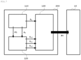
- FIG. 1 is a block diagram showing a schematic configuration of a high-frequency power supply device according to Embodiment 1 which is a representative example of the invention
- FIG. 2 is a block diagram showing an example of a specific configuration of a synchronous pulse generation mechanism according to Embodiment 1;
- FIG. 3 is a block diagram showing an example of a specific configuration of an output level setting mechanism according to Embodiment 1;
- FIG. 4 is a block diagram showing an example of a specific configuration of an oscillation mechanism according to Embodiment 1;
- FIGS. 5 ( a ) to 5 ( e ) are a graph showing an example of an output waveform obtained by an output control method for the high-frequency power supply device according to Embodiment 1;
- FIGS. 6 ( a ) to 6 ( e ) are a graph showing a variation of the output waveform obtained by the output control method for the high-frequency power supply device according to Embodiment 1;
- FIG. 7 is a block diagram showing a schematic configuration of a high-frequency power supply device according to Embodiment 2;
- FIG. 8 is a block diagram showing an example of a specific configuration of an output level setting mechanism according to Embodiment 2;
- FIG. 9 is a block diagram showing an example of a specific configuration of an oscillation mechanism according to Embodiment 2.
- FIGS. 10 ( a ) to 10 ( e ) are a graph showing an example of an output waveform obtained by an output control method for the high-frequency power supply device according to Embodiment 2.
- FIGS. 1 to 10 ( e ) A description will now be made about representative illustrative embodiments of a high-frequency power supply device and an output control method therefor according to the present invention by referring to FIGS. 1 to 10 ( e ).
- FIG. 1 is a block diagram that shows a schematic configuration of a high-frequency power supply device according to Embodiment 1 which is a representative example of the invention.
- a high-frequency power supply device 100 includes, by way of example, a synchronous pulse generation mechanism 110 that generates a synchronous pulse P 1 that includes output level information and output timing information of a high-frequency pulse PO to be output, an output level setting mechanism 120 that generates output level signals S L1 , S L2 for setting output levels of the high-frequency pulse PO based on the output level information of the synchronous pulse P 1 , and an oscillation mechanism 130 that receives a period reference signal S s based on the output timing information of the synchronous pulse P 1 and the above-mentioned output level signals S L1 , S L2 to thereby oscillate the high-frequency pulse PO.
- the high-frequency pulse PO output from the high-frequency power supply device 100 is fed to a target device 10 , such as plasma or laser generation device, induction
- FIG. 2 is a block diagram showing an example of a specific configuration of the synchronous pulse generation mechanism according to Embodiment 1.
- the synchronous pulse generation mechanism 110 of Embodiment 1 includes a synchronous pulse formation circuit 112 that forms the above-mentioned synchronous pulse P 1 , a period reference signal generation unit 114 that generates the period reference signal S s at a period reference time in the synchronous pulse P 1 , and a clocking mechanism 116 that clocks an output stop time based on the period reference signal S s to send out an output stop signal S T to the output level setting mechanism 120 .
- the synchronous pulse P 1 output from the synchronous pulse formation circuit 112 is also fed to the output level setting mechanism 120 , which will be described later.
- the synchronous pulse formation circuit 112 includes output level information (amplitude value) and output timing information (amplitude changing timing), by way of example, and outputs an approximately rectangular periodic pulse waveform that defines two output levels L 1 , L 2 on a vertical axis with respect to an elapsed time on a horizontal axis.
- FIG. 2 illustrates the case where the output levels are the high level L 1 and the low level L 2
- the pulse waveform may have three or more output levels as long as the waveform is an approximately rectangular periodic wave.
- the synchronous pulse P 1 is not limited to the rectangular wave, and may include any waveform that contains the output level information and the output timing information, such as sine wave or extremely-short pulse. Furthermore, the synchronous pulse P 1 may consist of a plurality of signal waveforms. For example, there is a technique for performing AND operation on a plurality of signal waveforms to obtain an output level and output timing.
- the period reference signal generation unit 114 uses the synchronous pulse P 1 received from the synchronous pulse formation circuit 112 to identify the output timing information which is a time reference of a period as one of the features of this synchronous pulse P 1 , and outputs the period reference signal S s at the identified timing.
- the time reference of the period is a time of switching from the low level L 2 to the high level L 1 (rising time), by way of example.
- the number of the period reference signals S s is not limited to one in one period, and for example, a time of switching from the high level L 1 to the low level L 2 (falling time) may be employed, in addition to the above-mentioned rising time from the low level L 2 to the high level L 1 .
- the clocking mechanism 116 is configured, by way of example, to receive the period reference signal S s from the period reference signal generation unit 114 , and then continue to send out an output stop signal S T to the output level setting mechanism 120 , which will be described later, from the time of receiving the period reference signal until after a lapse of a predetermined output stop time.
- the clocking mechanism 116 is configured such that any timing can be selected for the predetermined output stop time with respect to a clock period of a clock pulse generator 132 , which will be described later (see FIG. 4 ). This enables to arbitrarily select timing when the sending of the output stop signal S T is stopped.
- FIG. 3 is a block diagram showing an example of a specific configuration of the output level setting mechanism according to Embodiment 1.
- the output level setting mechanism 120 of Embodiment 1 includes a level determination unit 122 for issuing a first level setting command S 1 or second level setting command S 2 in accordance with an amplitude value (output level information) of the synchronous pulse P 1 , and a level setting signal generation unit 124 for generating level setting signals (first level setting signal S L1 and second level setting signal S L2 ) in response to the output stop signal S T as well as the first level setting command S 1 and the second level setting command S 2 .
- the level setting signal generation unit 124 includes a first level setting signal generator 126 for generating the first level setting signal S L1 while the first level setting command S 1 is being received, and a second level setting signal generator 128 for generating the second level setting signal S L2 while the second level setting command S 2 is being received.
- the level determination unit 122 is configured to receive the synchronous pulse P 1 from the synchronous pulse formation circuit 112 , and send out a predetermined setting command in real time according to the output level of the received synchronous pulse P 1 .
- the level determination unit 122 in Embodiment 1 sends out the first level setting command S 1 while the synchronous pulse P 1 is at the high level L 1 , and when the level of the synchronous pulse P 1 is changed to the low level L 2 , sends out the second level setting command S 2 .
- the first level setting signal generator 126 generates the first level setting signal S L1 in response to the first level setting command S 1 received from the level determination unit 122 .
- the second level setting signal generator 128 generates the second level setting signal S L2 in response to the second level setting command S 2 received from the level determination unit 122 .
- the level setting signal generation unit 124 is configured not to output the first level setting signal S L1 generated by the first level setting signal generator 126 or the second level setting signal S L2 generated by the second level setting signal generator 128 to the oscillation mechanism 130 while receiving the output stop signal S T from the synchronous pulse generation mechanism 110 .
- FIG. 4 is a block diagram showing an example of a specific configuration of the oscillation mechanism according to Embodiment 1.
- the oscillation mechanism 130 includes a clock pulse generator 132 for generating a clock pulse P 2 in a predetermined high frequency range, and an oscillation amplifier 134 for receiving the period reference signal S s from the synchronous pulse generation mechanism 110 , the first level setting signal S L1 and the second level setting signal S L2 from the output level setting mechanism 120 , and the above-mentioned clock pulse P 2 , so as to form a high-frequency pulse PO based on these signals.
- the clock pulse generator 132 is for generating the clock pulse P 2 at high frequency (several hundreds of kHz to several tens of MHz) according to the output of the high-frequency pulse PO, e.g., generating the clock pulse P 2 of 13.56 MHz. Moreover, in addition to generating the above-described clock pulse P 2 at a certain high frequency at regular intervals, the clock pulse generator 132 has another function of resetting timing of the generation of the clock pulse P 2 (set to a desired phase) at a desired time t rst (see FIGS. 5 ( a ) to 5 ( e ) or 6 ( a ) to 6 ( e )).
- the oscillation amplifier 134 determines oscillation timing for the high-frequency pulse PO based on the period reference signal S s , and amplifies the amplitude value of the clock pulse P 2 based on the first level setting signal S L1 and the second level setting signal S L2 to generate the high-frequency pulse PO.
- FIGS. 5 ( a ) to 5 ( e ) are a graph showing an example of an output waveform that can be obtained by an output control method for the high-frequency power supply device according to Embodiment 1.
- the synchronous pulse P 1 formed by the synchronous pulse formation circuit 112 in the synchronous pulse generation mechanism 110 is formed as a periodic pulse signal that will be at the high level L 1 at an interval of a time T L1 and at the low level L 2 at an interval of a time T L2 .
- a rising time to the high level L 1 which is a time reference of one pulse period, is derived from the concerned synchronous pulse P 1 , and the period reference signal generation unit 114 sends out the period reference signal S s at each rising time, by way of example.
- the synchronous pulse P 1 is also fed to the output level setting mechanism 120 , and the level determination unit 122 in the output level setting mechanism 120 sets an output level for each time, so that the first level setting signal generator 126 or the second level setting signal generator 128 sends out the first level setting signal S L1 or the second level setting signal S L2 to the oscillation mechanism 130 . That is to say, by referring to FIG. 5 ( a ) , the first level setting signal S L1 is sent out at the interval of the time T L1 and the second level setting signal S L2 is sent out at the interval of the time T L2 .
- the oscillation amplifier 134 in the oscillation mechanism 130 amplifies an amplitude value of the clock pulse P 2 in accordance with the received first level setting signal S L1 or second level setting signal S L2 . More specifically, when the first level setting signals S L1 are received repeatedly, consecutive pulses having average height of the clock pulse P 2 at the high level L 1 are output as shown in FIG. 5 ( b ) . When the second level setting signals S L2 are received repeatedly, consecutive pulses having average height of the clock pulse P 2 at the low level L 2 are output as shown in FIG. 5 ( c ) .
- the output level setting mechanism 120 is configured not to send out the first level setting signal S L1 while the output stop signal S T is being received, the continuous pulses at the high level L 1 are not output from the start of the interval of the time T L1 until after a lapse of the output stop time T st .
- the timing of the reset time t rst is defined in accordance with a phase ⁇ st of the high-frequency pulse PO that is firstly output after the expiration of the output stop time T st . More specifically, a phase of the clock pulse P 2 is reset at the reset time t rst , so that the phase of the high-frequency pulse PO after the lapse of the output stop time T st will be the same phase at all times.
- FIGS. 6 ( a ) to 6 ( e ) are a graph showing a variation of an output waveform obtained by the output control method for the high-frequency power supply device according to Embodiment 1. As shown in FIG. 6 ( a ) , in the output control method for the high-frequency power supply device according to the variation shown in FIGS. 6 ( a ) to 6 ( e ) .
- a rising time to the high level L 1 which is a time reference of one pulse period, is firstly derived from a synchronous pulse P 1 formed by the synchronous pulse formation circuit 112 in the synchronous pulse generation mechanism 110 , and the period reference signal generation unit 114 sends out a period reference signal S s at each rising time, as with the case shown in FIGS. 5 ( a ) to 5 ( e ) .
- the output level setting mechanism 120 sends out a first level setting signal S L1 at an interval of a time T L1 and a second level setting signal S L2 at an interval of a time T L2 to the oscillation mechanism 130 .
- the oscillation amplifier 134 in the oscillation mechanism 130 amplifies an amplitude value of a clock pulse P 2 in accordance with the received first level setting signal S L1 or second level setting signal S L2 . Then, consecutive pulses having average height of the clock pulse P 2 at the high level L 1 as shown in FIG. 6 ( b ) and consecutive pulses having average height of a clock pulse P 2 at a low level L 2 as shown in FIG. 6 ( c ) are output.
- the output level setting mechanism 120 is configured not to send out the first level setting signal S L1 while receiving the output stop signal S T , when this operation is performed continuously over time from the generation of the synchronous pulse P 1 , the outputting of a high-frequency pulse PO is started at a time of receiving the period reference signal S s by the oscillation mechanism 130 , and thereby the continuous pulses at the high level L 1 are output at the interval of time T L1 , as shown in FIG. 6 ( e ) .
- the continuous pulses at the low level L 2 are output at the interval of the time T L2 .
- timing of the reset time t rst is set such that a phase ⁇ st of the high-frequency pulse PO, which is the first to be output after a lapse of the output stop time T st , is zero at all times.
- the reset of the phase of the clock pulse P 2 at the reset time test enables to stably output the high-frequency pulse PO after the lapse of the output stop time T st such that the phase of the pulse PO is zero at all times, and yet at the same time, the outputting of the pulse PO delays by a waiting time a for matching output phases to be zero, as shown in FIG. 6 ( e ) .
- the high-frequency power supply device and the output control method therefor are adapted to receive the period reference signal S s based on the synchronous pulse P 1 , the first level setting signal S L1 , the second level setting signal S L2 and the clock pulse P 2 , and when forming the high-frequency pulse PO based on these signals, set the output stop time T s clocked based on the period reference signal S s to be integral multiple of the clock period of the clock pulse P 2 , and thereby the output level setting mechanism stops sending out the first level setting signal S L1 or second level setting signal S L2 while the output stop signal S T is being received, so that the phases of the output high-frequency pulse can be matched on all occasions even if the synchronous pulse and the clock pulse are generated separately.
- FIG. 7 is a block diagram showing a schematic configuration of a high-frequency power supply device according to Embodiment 2.
- constituent elements of a high-frequency power supply device 200 according to Embodiment 2 that are the same as or similar to those of Embodiment 1 will be denoted by the same reference numerals in Embodiment 1, and the descriptions about them will not be repeated.
- the high-frequency power supply device 200 includes a synchronous pulse generation mechanism 110 , an output level setting mechanism 120 and an oscillation mechanism 130 .
- the high-frequency power supply device 200 of Embodiment 2 differs from the high-frequency power supply device 100 of Embodiment 1 in that the output level setting mechanism 120 sends out a level-zero signal S L0 to the oscillation mechanism 130 .
- FIG. 8 is a block diagram showing an example of a specific configuration of the output level setting mechanism according to Embodiment 2.
- the output level setting mechanism 120 according to Embodiment 2 includes a level determination unit 122 that receives an output stop signal S T and a synchronous pulse P 1 , and issues a first level setting command S 1 or second level setting command S 2 in accordance with an amplitude value (output level) of the synchronous pulse P 1 , and a level setting signal generation unit 124 that generates level setting signals (level-zero signal S L0 , first level setting signal S L1 and second level setting signal S L2 ) in response to the output stop signal S T as well as the first level setting command S 1 and the second level setting command S 2 .
- level determination unit 122 that receives an output stop signal S T and a synchronous pulse P 1 , and issues a first level setting command S 1 or second level setting command S 2 in accordance with an amplitude value (output level) of the synchronous pulse P 1
- the level setting signal generation unit 124 includes a level-zero signal generator 223 that generates the level-zero signal S L0 based on the output stop signal S T , and a first level setting signal generator 126 and a second level setting signal generator 128 , which are similar to those of Embodiment 1.
- the level determination unit 122 is configured, as with the case of Embodiment 1, to receive the synchronous pulse P 1 from the synchronous pulse formation circuit 112 , and according to the output level of the synchronous pulse P 1 , send out the first level setting command S 1 while the synchronous pulse P 1 is at a high level L 1 and send out the second level setting command S 2 when the level of the synchronous pulse P 1 is changed to a low level L 2 .
- the level-zero signal generator 223 is configured to be activated while the level setting signal generation unit 124 is receiving the output stop signal S T , and send out the level-zero signal S L0 that makes an amplitude value of a high-frequency pulse PO to be zero while the output stop signal S T is being received.
- the first level setting signal generator 126 and the second level setting signal generator 128 are configured, as with the case of Embodiment 1, to receive the first level setting command S 1 or second level setting command S 2 from the level determination unit 122 to thereby send out the first level setting signal S L1 or second level setting signal S L2 to the oscillation mechanism 130 .
- the level setting signal generation unit 124 outputs only the level-zero signal Sm to the oscillation mechanism 130 and does not output the first level setting signal S L1 or second level setting signal S L2 while receiving the output stop signal S T from the synchronous pulse generation mechanism 110 .
- FIG. 9 is a block diagram showing an example of a specific configuration of the oscillation mechanism according to Embodiment 2.
- the oscillation mechanism 130 of Embodiment 2 includes a clock pulse generator 132 , and an oscillation amplifier 234 that receives a period reference signal S s from the synchronous pulse generation mechanism 110 , the level-zero signal S L0 , the first level setting signal S L1 and the second level setting signal S L2 from the output level setting mechanism 120 , and the clock pulse P 2 , so as to form a high-frequency pulse PO based on these signals.
- the oscillation amplifier 234 is configured to determine oscillation timing for the high-frequency pulse PO based on the period reference signal S s , and define an amplitude value of the high-frequency pulse PO to be zero while receiving the level-zero signal S L0 .
- the oscillation amplifier 234 amplifies the amplitude value of the clock pulse P 2 to be at a high level L 1 or low level L 2 based on the received signals, so as to generate the high-frequency pulse PO.
- FIGS. 10 ( a ) to 10 ( e ) are a graph showing an example of an output waveform obtained by the high-frequency power supply device and an output control method therefor according to Embodiment 2.
- the output control method for the high-frequency power supply device according to Embodiment 2 the relationship between a synchronous pulse P 1 and an output stop signal S T shown in FIGS. 10 ( a ) to 10 ( d ) and amplification of amplitude values with respect to a high level L 1 and a low level L 2 of a high-frequency pulse PO is the same as the relationship in Embodiment 1, and thus a description about it will not be repeated in here.
- the output level setting mechanism controls the outputting of the level-zero signal Z L0 for making the output level to be zero to the oscillation mechanism while the output stop signal S T is being output, thereby enabling to perform the control such that even if a dummy bounce pulse (damping pulse P D ) is produced due to the switching of the output level at an end of an output interval (time T L2 ) of a last high-frequency pulse PO, an erroneous pulse output is prevented by making an amplitude value in an actual output to be zero, as shown in FIG. 9 ( e ) .
- Embodiments 1 and 2 illustrate that the output stop time T st is set at the early outputting stages at the high level L 1 .
- the output stop time T st can be set at the early outputting stages at the low level L 2 , or at the early outputting stages at the high level L 1 and the low level L 2 . This makes it possible to control the wave number to be kept at a constant value for each period during outputting the high-frequency pulse PO.
- Embodiments 1 and 2 may not be separate constitutions of the invention, and may be applied as one high-frequency power supply device by combining their respective features.
Landscapes
- Physics & Mathematics (AREA)
- Engineering & Computer Science (AREA)
- Plasma & Fusion (AREA)
- Chemical & Material Sciences (AREA)
- Analytical Chemistry (AREA)
- Plasma Technology (AREA)
- Drying Of Semiconductors (AREA)
Abstract
Description
-
- [Patent Literature 1] Japanese Patent Laid-Open Publication No. H11-214363
- [Patent Literature 2] Japanese Patent Laid-Open Publication No. 2007-514300.
-
- 10 Target Device
- 100, 200, 300 High-Frequency Power Supply Device
- 110 Synchronous Pulse Generation Mechanism
- 112 Synchronous Pulse Formation Circuit
- 114 Period Reference Signal Generation Unit
- 116 Clocking Mechanism
- 120 Output Level Setting Mechanism
- 122 Level Determination Unit
- 124 Level Setting Signal Generation Unit
- 126 First Level Setting Signal Generator
- 128 Second Level Setting Signal Generator
- 130 Oscillation Mechanism
- 132 Clock Pulse Generator
- 134, 234 Oscillation Amplifier
- 223 Level-Zero Signal Generator
- PO High-Frequency Pulse
- P1 Synchronous Pulse
- P2 Clock Pulse
- Ss Period Reference Signal
- ST Output Stop Signal
- SL0 Level-Zero Signal
- SL1 First Level Setting Signal
- SL2 Second Level Setting Signal
- Tst Output Stop Time
Claims (6)
Applications Claiming Priority (3)
| Application Number | Priority Date | Filing Date | Title |
|---|---|---|---|
| JP2020045557A JP7383533B2 (en) | 2020-03-16 | 2020-03-16 | High frequency power supply device and its output control method |
| JP2020-045557 | 2020-03-16 | ||
| PCT/JP2021/008459 WO2021187137A1 (en) | 2020-03-16 | 2021-03-04 | High-frequency power supply device and output control method therefor |
Publications (2)
| Publication Number | Publication Date |
|---|---|
| US20230124064A1 US20230124064A1 (en) | 2023-04-20 |
| US12014899B2 true US12014899B2 (en) | 2024-06-18 |
Family
ID=77772045
Family Applications (1)
| Application Number | Title | Priority Date | Filing Date |
|---|---|---|---|
| US17/911,174 Active 2041-04-14 US12014899B2 (en) | 2020-03-16 | 2021-03-04 | High-frequency power supply device and output control method therefor |
Country Status (7)
| Country | Link |
|---|---|
| US (1) | US12014899B2 (en) |
| EP (1) | EP4124181A4 (en) |
| JP (1) | JP7383533B2 (en) |
| KR (1) | KR102873346B1 (en) |
| CN (1) | CN115316047A (en) |
| TW (1) | TWI848209B (en) |
| WO (1) | WO2021187137A1 (en) |
Families Citing this family (1)
| Publication number | Priority date | Publication date | Assignee | Title |
|---|---|---|---|---|
| CN113459971B (en) * | 2021-06-27 | 2023-10-03 | 深圳新联胜光电科技有限公司 | A vehicle driving data collection method and system |
Citations (10)
| Publication number | Priority date | Publication date | Assignee | Title |
|---|---|---|---|---|
| JPH11214363A (en) | 1998-01-23 | 1999-08-06 | Hitachi Ltd | Semiconductor manufacturing method and apparatus, and semiconductor element |
| US20050205532A1 (en) | 2003-11-07 | 2005-09-22 | Roger Patrick | Methods and apparatus for optimizing a substrate in a plasma processing system |
| US20070076344A1 (en) | 2005-09-30 | 2007-04-05 | Daihen Corporation | High frequency power device |
| US20140009073A1 (en) | 2012-02-22 | 2014-01-09 | Lam Research Corporation | Adjustment of Power and Frequency Based on Three or More States |
| US20140361690A1 (en) | 2011-12-27 | 2014-12-11 | Tokyo Electron Limited | Plasma processing apparatus |
| US20150122421A1 (en) | 2013-11-05 | 2015-05-07 | Tokyo Electron Limited | Plasma processing apparatus |
| US20160079037A1 (en) | 2014-09-17 | 2016-03-17 | Tokyo Electron Limited | Plasma processing apparatus |
| US20160299548A1 (en) | 2013-12-18 | 2016-10-13 | Trumpf Huettinger Gmbh + Co. Kg | Power Supply Systems and Methods for Generating Power |
| WO2019244734A1 (en) | 2018-06-22 | 2019-12-26 | 東京エレクトロン株式会社 | Control method and plasma treatment device |
| US20220301825A1 (en) * | 2019-11-26 | 2022-09-22 | Tokyo Electron Limited | Plasma processing method and plasma processing apparatus |
Family Cites Families (9)
| Publication number | Priority date | Publication date | Assignee | Title |
|---|---|---|---|---|
| CN1307407A (en) * | 2000-01-21 | 2001-08-08 | 周振权 | Pulse signal transmitting method in power line |
| JP3660636B2 (en) * | 2002-03-05 | 2005-06-15 | 株式会社日立ハイテクノロジーズ | High frequency power supply for plasma generator |
| JP2005045019A (en) * | 2003-07-22 | 2005-02-17 | Orc Mfg Co Ltd | Q switch laser device |
| JP4963023B2 (en) * | 2006-01-11 | 2012-06-27 | 株式会社アルバック | Sputtering method and sputtering apparatus |
| JP5319150B2 (en) * | 2008-03-31 | 2013-10-16 | 東京エレクトロン株式会社 | Plasma processing apparatus, plasma processing method, and computer-readable storage medium |
| JP2010238881A (en) * | 2009-03-31 | 2010-10-21 | Tokyo Electron Ltd | Plasma processing apparatus and plasma processing method |
| JP2011029069A (en) * | 2009-07-28 | 2011-02-10 | Mitsubishi Electric Corp | Plasma processing device, and method of manufacturing semiconductor film |
| JP5485053B2 (en) * | 2010-07-14 | 2014-05-07 | 新電元工業株式会社 | Semiconductor device, firing angle conversion circuit, power supply device, lighting device, and signal conversion method |
| JP6512962B2 (en) * | 2014-09-17 | 2019-05-15 | 東京エレクトロン株式会社 | Plasma processing system |
-
2020
- 2020-03-16 JP JP2020045557A patent/JP7383533B2/en active Active
-
2021
- 2021-03-03 TW TW110107467A patent/TWI848209B/en active
- 2021-03-04 CN CN202180021281.7A patent/CN115316047A/en active Pending
- 2021-03-04 US US17/911,174 patent/US12014899B2/en active Active
- 2021-03-04 KR KR1020227034825A patent/KR102873346B1/en active Active
- 2021-03-04 EP EP21771286.8A patent/EP4124181A4/en active Pending
- 2021-03-04 WO PCT/JP2021/008459 patent/WO2021187137A1/en not_active Ceased
Patent Citations (15)
| Publication number | Priority date | Publication date | Assignee | Title |
|---|---|---|---|---|
| JPH11214363A (en) | 1998-01-23 | 1999-08-06 | Hitachi Ltd | Semiconductor manufacturing method and apparatus, and semiconductor element |
| US20050205532A1 (en) | 2003-11-07 | 2005-09-22 | Roger Patrick | Methods and apparatus for optimizing a substrate in a plasma processing system |
| JP2007514300A (en) | 2003-11-07 | 2007-05-31 | ラム リサーチ コーポレーション | Method and apparatus for optimizing a substrate in a plasma processing system |
| US20070076344A1 (en) | 2005-09-30 | 2007-04-05 | Daihen Corporation | High frequency power device |
| JP2007103102A (en) | 2005-09-30 | 2007-04-19 | Daihen Corp | High frequency power supply |
| US20140361690A1 (en) | 2011-12-27 | 2014-12-11 | Tokyo Electron Limited | Plasma processing apparatus |
| US20140009073A1 (en) | 2012-02-22 | 2014-01-09 | Lam Research Corporation | Adjustment of Power and Frequency Based on Three or More States |
| US20150122421A1 (en) | 2013-11-05 | 2015-05-07 | Tokyo Electron Limited | Plasma processing apparatus |
| US20160299548A1 (en) | 2013-12-18 | 2016-10-13 | Trumpf Huettinger Gmbh + Co. Kg | Power Supply Systems and Methods for Generating Power |
| JP2017512355A (en) | 2013-12-18 | 2017-05-18 | トゥルンプフ ヒュッティンガー ゲゼルシャフト ミット ベシュレンクテル ハフツング ウント コンパニー コマンディートゲゼルシャフトTRUMPF Huettinger GmbH + Co. KG | Power supply system and method for forming power |
| US20160079037A1 (en) | 2014-09-17 | 2016-03-17 | Tokyo Electron Limited | Plasma processing apparatus |
| WO2019244734A1 (en) | 2018-06-22 | 2019-12-26 | 東京エレクトロン株式会社 | Control method and plasma treatment device |
| JP2020004710A (en) | 2018-06-22 | 2020-01-09 | 東京エレクトロン株式会社 | Control method and plasma treatment device |
| US20200411286A1 (en) | 2018-06-22 | 2020-12-31 | Tokyo Electron Limited | Control method and plasma processing apparatus |
| US20220301825A1 (en) * | 2019-11-26 | 2022-09-22 | Tokyo Electron Limited | Plasma processing method and plasma processing apparatus |
Non-Patent Citations (3)
| Title |
|---|
| Extended (Supplementary) European Search Report dated Feb. 27, 2024, issued in counterpart application No. 21771286.8. (8 pages). |
| International Search Report dated May 25, 2021, issued in counterpart Application No. PCT/JP2021/008459. (2 pages). |
| Office Action dated Sep. 5, 2023, issued in counterpart JP application No. 2020-045557, with English translation. (6 pages). |
Also Published As
| Publication number | Publication date |
|---|---|
| JP2021150031A (en) | 2021-09-27 |
| TWI848209B (en) | 2024-07-11 |
| KR102873346B1 (en) | 2025-10-20 |
| TW202141587A (en) | 2021-11-01 |
| CN115316047A (en) | 2022-11-08 |
| EP4124181A1 (en) | 2023-01-25 |
| JP7383533B2 (en) | 2023-11-20 |
| KR20220154147A (en) | 2022-11-21 |
| WO2021187137A1 (en) | 2021-09-23 |
| US20230124064A1 (en) | 2023-04-20 |
| EP4124181A4 (en) | 2024-03-27 |
Similar Documents
| Publication | Publication Date | Title |
|---|---|---|
| JP7155354B2 (en) | Plasma processing apparatus, processor, control method, non-transitory computer-readable recording medium and program | |
| TWI856971B (en) | Radio frequency (rf) pulsing impedance tuning with multiplier mode | |
| KR102467354B1 (en) | Smart RF pulsing tuning using variable frequency generators | |
| JP5822795B2 (en) | Plasma processing equipment | |
| KR101787501B1 (en) | System and methods of bimodal automatic power and frequency tuning of rf generators | |
| US8952634B2 (en) | Programmable radio frequency waveform generator for a synchrocyclotron | |
| US8899247B2 (en) | Ultrasonic cleaning apparatus | |
| US10037868B2 (en) | Plasma processing apparatus | |
| KR101519516B1 (en) | Pulse shaping and power control of the pulsed co2 laser output | |
| CN115280903B (en) | High-frequency power supply device and output control method thereof | |
| JP2003505868A (en) | Apparatus and method for etching a substrate using inductively coupled plasma | |
| US12014899B2 (en) | High-frequency power supply device and output control method therefor | |
| CN105914123B (en) | Method and apparatus for controlling plasma in a plasma processing system | |
| JP2023519205A (en) | Controllers and control techniques for linear accelerators and ion implanters with linear accelerators | |
| JPWO2018037440A1 (en) | Time-of-flight mass spectrometer | |
| US7554414B2 (en) | Fast starting circuit for crystal oscillators | |
| WO1997027494A1 (en) | Delay time measuring method and pulse generator for measuring delay time for use in said measuring method | |
| JPH06168799A (en) | Timing control device | |
| US20260045463A1 (en) | Data-Driven Method for Determining Resonant Frequencies in Plasma Process Systems with Multiple Plasma States | |
| JPH0628244B2 (en) | Excitation control device for laser amplifier device |
Legal Events
| Date | Code | Title | Description |
|---|---|---|---|
| AS | Assignment |
Owner name: KYOSAN ELECTRIC MFG. CO., LTD., JAPAN Free format text: ASSIGNMENT OF ASSIGNORS INTEREST;ASSIGNORS:FUJIWARA, TAKESHI;YASUDA, YUYA;KATAFUCHI, RYUHEI;AND OTHERS;REEL/FRAME:061074/0046 Effective date: 20220708 |
|
| FEPP | Fee payment procedure |
Free format text: ENTITY STATUS SET TO UNDISCOUNTED (ORIGINAL EVENT CODE: BIG.); ENTITY STATUS OF PATENT OWNER: LARGE ENTITY |
|
| STPP | Information on status: patent application and granting procedure in general |
Free format text: DOCKETED NEW CASE - READY FOR EXAMINATION |
|
| STPP | Information on status: patent application and granting procedure in general |
Free format text: EX PARTE QUAYLE ACTION MAILED |
|
| STPP | Information on status: patent application and granting procedure in general |
Free format text: RESPONSE TO EX PARTE QUAYLE ACTION ENTERED AND FORWARDED TO EXAMINER |
|
| STPP | Information on status: patent application and granting procedure in general |
Free format text: NOTICE OF ALLOWANCE MAILED -- APPLICATION RECEIVED IN OFFICE OF PUBLICATIONS |
|
| STPP | Information on status: patent application and granting procedure in general |
Free format text: AWAITING TC RESP., ISSUE FEE NOT PAID |
|
| STPP | Information on status: patent application and granting procedure in general |
Free format text: NOTICE OF ALLOWANCE MAILED -- APPLICATION RECEIVED IN OFFICE OF PUBLICATIONS |
|
| STPP | Information on status: patent application and granting procedure in general |
Free format text: PUBLICATIONS -- ISSUE FEE PAYMENT VERIFIED |
|
| STCF | Information on status: patent grant |
Free format text: PATENTED CASE |