US12014692B2 - Display driving module, method for driving the same and display device - Google Patents
Display driving module, method for driving the same and display device Download PDFInfo
- Publication number
- US12014692B2 US12014692B2 US17/626,467 US202117626467A US12014692B2 US 12014692 B2 US12014692 B2 US 12014692B2 US 202117626467 A US202117626467 A US 202117626467A US 12014692 B2 US12014692 B2 US 12014692B2
- Authority
- US
- United States
- Prior art keywords
- electrically connected
- control
- multiplexing
- transistor
- electrode
- Prior art date
- Legal status (The legal status is an assumption and is not a legal conclusion. Google has not performed a legal analysis and makes no representation as to the accuracy of the status listed.)
- Active, expires
Links
Images


Classifications
-
- G—PHYSICS
- G09—EDUCATION; CRYPTOGRAPHY; DISPLAY; ADVERTISING; SEALS
- G09G—ARRANGEMENTS OR CIRCUITS FOR CONTROL OF INDICATING DEVICES USING STATIC MEANS TO PRESENT VARIABLE INFORMATION
- G09G3/00—Control arrangements or circuits, of interest only in connection with visual indicators other than cathode-ray tubes
- G09G3/20—Control arrangements or circuits, of interest only in connection with visual indicators other than cathode-ray tubes for presentation of an assembly of a number of characters, e.g. a page, by composing the assembly by combination of individual elements arranged in a matrix no fixed position being assigned to or needed to be assigned to the individual characters or partial characters
- G09G3/22—Control arrangements or circuits, of interest only in connection with visual indicators other than cathode-ray tubes for presentation of an assembly of a number of characters, e.g. a page, by composing the assembly by combination of individual elements arranged in a matrix no fixed position being assigned to or needed to be assigned to the individual characters or partial characters using controlled light sources
- G09G3/30—Control arrangements or circuits, of interest only in connection with visual indicators other than cathode-ray tubes for presentation of an assembly of a number of characters, e.g. a page, by composing the assembly by combination of individual elements arranged in a matrix no fixed position being assigned to or needed to be assigned to the individual characters or partial characters using controlled light sources using electroluminescent panels
- G09G3/32—Control arrangements or circuits, of interest only in connection with visual indicators other than cathode-ray tubes for presentation of an assembly of a number of characters, e.g. a page, by composing the assembly by combination of individual elements arranged in a matrix no fixed position being assigned to or needed to be assigned to the individual characters or partial characters using controlled light sources using electroluminescent panels semiconductive, e.g. using light-emitting diodes [LED]
- G09G3/3208—Control arrangements or circuits, of interest only in connection with visual indicators other than cathode-ray tubes for presentation of an assembly of a number of characters, e.g. a page, by composing the assembly by combination of individual elements arranged in a matrix no fixed position being assigned to or needed to be assigned to the individual characters or partial characters using controlled light sources using electroluminescent panels semiconductive, e.g. using light-emitting diodes [LED] organic, e.g. using organic light-emitting diodes [OLED]
- G09G3/3275—Details of drivers for data electrodes
- G09G3/3291—Details of drivers for data electrodes in which the data driver supplies a variable data voltage for setting the current through, or the voltage across, the light-emitting elements
-
- G—PHYSICS
- G09—EDUCATION; CRYPTOGRAPHY; DISPLAY; ADVERTISING; SEALS
- G09G—ARRANGEMENTS OR CIRCUITS FOR CONTROL OF INDICATING DEVICES USING STATIC MEANS TO PRESENT VARIABLE INFORMATION
- G09G2300/00—Aspects of the constitution of display devices
- G09G2300/04—Structural and physical details of display devices
- G09G2300/0421—Structural details of the set of electrodes
- G09G2300/0426—Layout of electrodes and connections
-
- G—PHYSICS
- G09—EDUCATION; CRYPTOGRAPHY; DISPLAY; ADVERTISING; SEALS
- G09G—ARRANGEMENTS OR CIRCUITS FOR CONTROL OF INDICATING DEVICES USING STATIC MEANS TO PRESENT VARIABLE INFORMATION
- G09G2300/00—Aspects of the constitution of display devices
- G09G2300/08—Active matrix structure, i.e. with use of active elements, inclusive of non-linear two terminal elements, in the pixels together with light emitting or modulating elements
- G09G2300/0809—Several active elements per pixel in active matrix panels
- G09G2300/0842—Several active elements per pixel in active matrix panels forming a memory circuit, e.g. a dynamic memory with one capacitor
- G09G2300/0852—Several active elements per pixel in active matrix panels forming a memory circuit, e.g. a dynamic memory with one capacitor being a dynamic memory with more than one capacitor
-
- G—PHYSICS
- G09—EDUCATION; CRYPTOGRAPHY; DISPLAY; ADVERTISING; SEALS
- G09G—ARRANGEMENTS OR CIRCUITS FOR CONTROL OF INDICATING DEVICES USING STATIC MEANS TO PRESENT VARIABLE INFORMATION
- G09G2310/00—Command of the display device
- G09G2310/02—Addressing, scanning or driving the display screen or processing steps related thereto
- G09G2310/0264—Details of driving circuits
- G09G2310/0286—Details of a shift registers arranged for use in a driving circuit
-
- G—PHYSICS
- G09—EDUCATION; CRYPTOGRAPHY; DISPLAY; ADVERTISING; SEALS
- G09G—ARRANGEMENTS OR CIRCUITS FOR CONTROL OF INDICATING DEVICES USING STATIC MEANS TO PRESENT VARIABLE INFORMATION
- G09G2310/00—Command of the display device
- G09G2310/02—Addressing, scanning or driving the display screen or processing steps related thereto
- G09G2310/0264—Details of driving circuits
- G09G2310/0297—Special arrangements with multiplexing or demultiplexing of display data in the drivers for data electrodes, in a pre-processing circuitry delivering display data to said drivers or in the matrix panel, e.g. multiplexing plural data signals to one D/A converter or demultiplexing the D/A converter output to multiple columns
-
- G—PHYSICS
- G09—EDUCATION; CRYPTOGRAPHY; DISPLAY; ADVERTISING; SEALS
- G09G—ARRANGEMENTS OR CIRCUITS FOR CONTROL OF INDICATING DEVICES USING STATIC MEANS TO PRESENT VARIABLE INFORMATION
- G09G2320/00—Control of display operating conditions
- G09G2320/02—Improving the quality of display appearance
- G09G2320/0209—Crosstalk reduction, i.e. to reduce direct or indirect influences of signals directed to a certain pixel of the displayed image on other pixels of said image, inclusive of influences affecting pixels in different frames or fields or sub-images which constitute a same image, e.g. left and right images of a stereoscopic display
-
- G—PHYSICS
- G09—EDUCATION; CRYPTOGRAPHY; DISPLAY; ADVERTISING; SEALS
- G09G—ARRANGEMENTS OR CIRCUITS FOR CONTROL OF INDICATING DEVICES USING STATIC MEANS TO PRESENT VARIABLE INFORMATION
- G09G3/00—Control arrangements or circuits, of interest only in connection with visual indicators other than cathode-ray tubes
- G09G3/20—Control arrangements or circuits, of interest only in connection with visual indicators other than cathode-ray tubes for presentation of an assembly of a number of characters, e.g. a page, by composing the assembly by combination of individual elements arranged in a matrix no fixed position being assigned to or needed to be assigned to the individual characters or partial characters
- G09G3/22—Control arrangements or circuits, of interest only in connection with visual indicators other than cathode-ray tubes for presentation of an assembly of a number of characters, e.g. a page, by composing the assembly by combination of individual elements arranged in a matrix no fixed position being assigned to or needed to be assigned to the individual characters or partial characters using controlled light sources
- G09G3/30—Control arrangements or circuits, of interest only in connection with visual indicators other than cathode-ray tubes for presentation of an assembly of a number of characters, e.g. a page, by composing the assembly by combination of individual elements arranged in a matrix no fixed position being assigned to or needed to be assigned to the individual characters or partial characters using controlled light sources using electroluminescent panels
- G09G3/32—Control arrangements or circuits, of interest only in connection with visual indicators other than cathode-ray tubes for presentation of an assembly of a number of characters, e.g. a page, by composing the assembly by combination of individual elements arranged in a matrix no fixed position being assigned to or needed to be assigned to the individual characters or partial characters using controlled light sources using electroluminescent panels semiconductive, e.g. using light-emitting diodes [LED]
- G09G3/3208—Control arrangements or circuits, of interest only in connection with visual indicators other than cathode-ray tubes for presentation of an assembly of a number of characters, e.g. a page, by composing the assembly by combination of individual elements arranged in a matrix no fixed position being assigned to or needed to be assigned to the individual characters or partial characters using controlled light sources using electroluminescent panels semiconductive, e.g. using light-emitting diodes [LED] organic, e.g. using organic light-emitting diodes [OLED]
- G09G3/3225—Control arrangements or circuits, of interest only in connection with visual indicators other than cathode-ray tubes for presentation of an assembly of a number of characters, e.g. a page, by composing the assembly by combination of individual elements arranged in a matrix no fixed position being assigned to or needed to be assigned to the individual characters or partial characters using controlled light sources using electroluminescent panels semiconductive, e.g. using light-emitting diodes [LED] organic, e.g. using organic light-emitting diodes [OLED] using an active matrix
- G09G3/3233—Control arrangements or circuits, of interest only in connection with visual indicators other than cathode-ray tubes for presentation of an assembly of a number of characters, e.g. a page, by composing the assembly by combination of individual elements arranged in a matrix no fixed position being assigned to or needed to be assigned to the individual characters or partial characters using controlled light sources using electroluminescent panels semiconductive, e.g. using light-emitting diodes [LED] organic, e.g. using organic light-emitting diodes [OLED] using an active matrix with pixel circuitry controlling the current through the light-emitting element
-
- G—PHYSICS
- G09—EDUCATION; CRYPTOGRAPHY; DISPLAY; ADVERTISING; SEALS
- G09G—ARRANGEMENTS OR CIRCUITS FOR CONTROL OF INDICATING DEVICES USING STATIC MEANS TO PRESENT VARIABLE INFORMATION
- G09G3/00—Control arrangements or circuits, of interest only in connection with visual indicators other than cathode-ray tubes
- G09G3/20—Control arrangements or circuits, of interest only in connection with visual indicators other than cathode-ray tubes for presentation of an assembly of a number of characters, e.g. a page, by composing the assembly by combination of individual elements arranged in a matrix no fixed position being assigned to or needed to be assigned to the individual characters or partial characters
- G09G3/22—Control arrangements or circuits, of interest only in connection with visual indicators other than cathode-ray tubes for presentation of an assembly of a number of characters, e.g. a page, by composing the assembly by combination of individual elements arranged in a matrix no fixed position being assigned to or needed to be assigned to the individual characters or partial characters using controlled light sources
- G09G3/30—Control arrangements or circuits, of interest only in connection with visual indicators other than cathode-ray tubes for presentation of an assembly of a number of characters, e.g. a page, by composing the assembly by combination of individual elements arranged in a matrix no fixed position being assigned to or needed to be assigned to the individual characters or partial characters using controlled light sources using electroluminescent panels
- G09G3/32—Control arrangements or circuits, of interest only in connection with visual indicators other than cathode-ray tubes for presentation of an assembly of a number of characters, e.g. a page, by composing the assembly by combination of individual elements arranged in a matrix no fixed position being assigned to or needed to be assigned to the individual characters or partial characters using controlled light sources using electroluminescent panels semiconductive, e.g. using light-emitting diodes [LED]
- G09G3/3208—Control arrangements or circuits, of interest only in connection with visual indicators other than cathode-ray tubes for presentation of an assembly of a number of characters, e.g. a page, by composing the assembly by combination of individual elements arranged in a matrix no fixed position being assigned to or needed to be assigned to the individual characters or partial characters using controlled light sources using electroluminescent panels semiconductive, e.g. using light-emitting diodes [LED] organic, e.g. using organic light-emitting diodes [OLED]
- G09G3/3266—Details of drivers for scan electrodes
Definitions
- the present disclosure relates to the field of display technology, and in particular to a display driving module, a method for driving the display driving module and a display device.
- a gaming phone equipped with a screen having a high frequency is one of hot spots in a mobile phone market. For a same animation, it shows smoother visual effects on the screen having the high frequency.
- the screen having the high frequency has a higher requirements on a display power consumption, a data charging time and a level of crosstalk. If a display of a conventional architecture is directly driven at the high frequency, it is unable to achieve good visual effects, and problems such as serious chromatic aberration and poor display uniformity caused by insufficient data charging time may occur.
- a dual data line technical solution in which pixel circuits in one column are controlled by two data lines, may be adopted.
- a screen refresh rate is doubled in the case that a frequency of a data voltage signal on each data line does not change.
- the crosstalk for display screen signal lines becomes more serious.
- a display driving module applied to a display device includes pixel circuits in multiple rows and multiple columns, the display driving module includes a gate driving circuit, and a plurality of data lines and a data driving circuit.
- the pixel circuits in odd-numbered rows and one column are electrically connected to a data line, and the pixel circuits in even-numbered rows and the one column are electrically connected to another data line.
- the data driving circuit includes a data driver and a multiplexing circuit, and the multiplexing circuit includes a first multiplexing sub-circuit and a second multiplexing sub-circuit.
- the first multiplexing sub-circuit is electrically connected to a first multiplexing control terminal, the data driver, the data lines electrically connected to the pixel circuits in odd-numbered rows and odd-numbered columns, and the data lines electrically connected to the pixel circuits in even-numbered rows and even-numbered columns, and configured to control the data driver to apply corresponding data voltages to the data lines electrically connected to the pixel circuits in odd-numbered rows and odd-numbered columns and the data lines electrically connected to the pixel circuits in even-numbered rows and even-numbered columns under the control of a first multiplexing control signal from the first multiplexing control terminal.
- the second multiplexing sub-circuit is electrically connected to a second multiplexing control terminal, the data driver, the data lines electrically connected to the pixel circuits in odd-numbered rows and even-numbered columns, and the data lines electrically connected to the pixel circuits in even-numbered rows and odd-numbered columns, and configured to control the data driver to apply corresponding data voltages to the data lines electrically connected to the pixel circuits in odd-numbered rows and even-numbered columns and the data lines electrically connected to the pixel circuits in even-numbered rows and odd-numbered columns under the control of a second multiplexing control signal from the second multiplexing control terminal.
- the gate driving circuit includes a plurality of levels of shift register units; and an n th -level shift register unit is electrically connected to the pixel circuits in a (2n ⁇ 1) th row and a (2n) th row, and configured to apply a same gate driving signal to the pixel circuits in the (2n ⁇ 1) th row and the (2n) th row, where n is a positive integer.
- the pixel circuits in odd-numbered rows and a (2m ⁇ 1) th column are electrically connected to a (4m ⁇ 3) th data line
- the pixel circuits in even-numbered rows and the (2m ⁇ 1)th column are electrically connected to a (4m ⁇ 2) th data line
- the pixel circuits in even-numbered rows and a (2m) th column are electrically connected to a (4m ⁇ 1) th data line
- the pixel circuits in odd-numbered rows and the (2m) th column are electrically connected to a (4m) th data line, where m is a positive integer.
- the first multiplexing sub-circuit includes at least one first multiplexing transistor and at least one second multiplexing transistor.
- a control electrode of the first multiplexing transistor is electrically connected to the first multiplexing control terminal, a first electrode of the first multiplexing transistor is electrically connected to the (4m ⁇ 3) th data line, and a second electrode of the first multiplexing transistor is electrically connected to the data driver.
- a control electrode of the second multiplexing transistor is electrically connected to the first multiplexing control terminal, a first electrode of the second multiplexing transistor is electrically connected to the (4m) th data line, and a second electrode of the second multiplexing transistor is electrically connected to the data driver.
- the second multiplexing sub-circuit includes at least one third multiplexing transistor and at least one fourth multiplexing transistor.
- a control electrode of the third multiplexing transistor is electrically connected to the second multiplexing control terminal, a first electrode of the third multiplexing transistor is electrically connected to the (4m ⁇ 2) th data line, and a second electrode of the third multiplexing transistor is electrically connected to the data driver.
- a control electrode of the fourth multiplexing transistor is electrically connected to the second multiplexing control terminal, a first electrode of the fourth multiplexing transistor is electrically connected to the (4m ⁇ 1) th data line, and a second electrode of the fourth multiplexing transistor is electrically connected to the data driver.
- the pixel circuits in even-numbered rows and a (2m ⁇ 1) th column are electrically connected to a (4m ⁇ 3) th data line
- the pixel circuits in odd-numbered rows and the (2m ⁇ 1) th column are electrically connected to a (4m ⁇ 2) th data line
- the pixel circuits in even-numbered rows and a (2m) th column are electrically connected to a (4m ⁇ 1) th data line
- the pixel circuits in odd-numbered rows and the (2m) th column are electrically connected to a (4m) th data line, where m is a positive integer.
- the first multiplexing sub-circuit includes at least one first multiplexing transistor and at least one second multiplexing transistor.
- a control electrode of the first multiplexing transistor is electrically connected to the first multiplexing control terminal, a first electrode of the first multiplexing transistor is electrically connected to the (4m ⁇ 2) th data line, and a second electrode of the first multiplexing transistor is electrically connected to the data driver.
- a control electrode of the second multiplexing transistor is electrically connected to the first multiplexing control terminal, a first electrode of the second multiplexing transistor is electrically connected to the (4m ⁇ 1) th data line, and a second electrode of the second multiplexing transistor is electrically connected to the data driver.
- the second multiplexing sub-circuit includes at least one third multiplexing transistor and at least one fourth multiplexing transistor.
- a control electrode of the third multiplexing transistor is electrically connected to the second multiplexing control terminal, a first electrode of the third multiplexing transistor is electrically connected to the (4m ⁇ 3) th data line, and a second electrode of the third multiplexing transistor is electrically connected to the data driver.
- a control electrode of the fourth multiplexing transistor is electrically connected to the second multiplexing control terminal, a first electrode of the fourth multiplexing transistor is electrically connected to the (4m) th data line, and a second electrode of the fourth multiplexing transistor is electrically connected to the data driver.
- the n th -level shift register unit includes a first one of n th -level shift register modules and a second one of n th -level shift register modules, and the pixel circuits are arranged in an active display region.
- the first one of the n th -level shift register modules is located at a first side of the active display region, and configured to apply the same gate driving signal to the pixel circuits in the (2n ⁇ 1) th row and the (2n) th row.
- the second one of the n th -level shift register modules is located at a second side of the active display region, and configured to apply the same gate driving signal to the pixel circuits in the (2n ⁇ 1) th row and the (2n) th row.
- the display drive module further includes a light-emitting control circuit, the light-emitting control circuit includes a plurality of levels of light-emitting control units; and an n th -level light-emitting control unit is electrically connected to the pixel circuits in the (2n ⁇ 1) th row and the (2n) th row, and configured to apply a same light-emitting control signal to the pixel circuits in the (2n ⁇ 1) th row and the (2n) th row, where n is a positive integer.
- the n th -level shift register unit includes an n th -level pull-up node control circuit, an n th -level pull-down control node control circuit, an n th -level pull-down node control circuit and an n th -level gate driving signal output circuit.
- the n th -level pull-up node control circuit is electrically connected to a first clock signal terminal, a first voltage terminal, an n th -level pull-up node and an n th -level pull-down control node, and configured to control the n th -level pull-up node to be electrically connected to the first voltage terminal under the control of a first clock signal from the first clock signal terminal, and control the n th -level pull-up node to be electrically connected to the first clock signal terminal and maintain a potential at the n th -level pull-up node under the control of a potential at the n th -level pull-down control node.
- the n th -level pull-down control node control circuit is electrically connected to an input terminal, the first clock signal terminal, a second clock signal terminal, the n th -level pull-up node, a second voltage terminal and the n th -level pull-down control node, and configured to control the n th -level pull-down control node to be electrically connected to the input terminal under the control of the first clock signal, control the n th -level pull-down control node to be electrically connected to the second voltage terminal under the control of the potential at the n th -level pull-up node and a second clock signal from the second clock signal terminal.
- the n th -level pull-down node control circuit is electrically connected to the n th -level pull-down control node, the first voltage terminal and the n th -level pull-down node, and configured to control the n th -level pull-down control node to be electrically connected to the n th -level pull-down node and maintain a potential at the n th -level pull-down node under the control of a first voltage signal from the first voltage terminal.
- the n th -level gate driving signal output circuit is electrically connected to the n th -level pull-up node, the n th -level pull-down node, the second voltage terminal, the second clock signal terminal and an n th -level gate driving signal output terminal, and configured to control the n th -level gate driving signal output terminal to be electrically connected to the second voltage terminal under the control of the potential at the n th -level pull-up node, and control the n th -level gate driving signal output terminal to be electrically connected to the second clock signal terminal under the control of the potential at the n th -level pull-down node.
- the n th -level gate driving signal output terminal is electrically connected to the pixel circuits in the (2n ⁇ 1) th row and the (2n) th row.
- the n th -level pull-up node control circuit includes a first scanning control transistor, a second scanning control transistor and a first scanning storage capacitor.
- a control electrode of the first scanning control transistor is electrically connected to the first clock signal terminal, a first electrode of the first scanning control transistor is electrically connected to the first voltage terminal, and a second electrode of the first scanning control transistor is electrically connected to the n th -level pull-up node.
- a control electrode of the second scanning control transistor is electrically connected to the n th -level pull-down control node, a first electrode of the second scanning control transistor is electrically connected to the n th -level pull-up node, and a second electrode of the second scanning control transistor is electrically connected to the first clock signal terminal.
- a first terminal of the first scanning storage capacitor is electrically connected to the n th -level pull-up node, and a second terminal of the first scanning storage capacitor is electrically connected to the second voltage terminal.
- the n th -level pull-down control node control circuit includes a third scanning control transistor, a fourth scanning control transistor and a fifth scanning control transistor.
- a control electrode of the third scanning control transistor is electrically connected to the first clock signal terminal, a first electrode of the third scanning control transistor is electrically connected to the input terminal, and a second electrode of the third scanning control transistor is electrically connected to the n th -level pull-down control node.
- a control electrode of the fourth scanning control transistor is electrically connected to the n th -level pull-up node, and a first electrode of the fourth scanning control transistor is electrically connected to the second voltage terminal.
- a control electrode of the fifth scanning control transistor is electrically connected to the second clock signal terminal, a first electrode of the fifth scanning control transistor is electrically connected to a second electrode of the fourth scanning control transistor, and a second electrode of the fifth scanning control transistor is electrically connected to the n th -level pull-down control node.
- the n th -level pull-down node control circuit includes a sixth scanning control transistor and a second scanning storage capacitor.
- a control electrode of the sixth scanning control transistor is electrically connected to the first voltage terminal, a first electrode of the sixth scanning control transistor is electrically connected to the n th -level pull-down control node, and a second electrode of the sixth scanning control transistor is electrically connected to the n th -level pull-down node.
- a first terminal of the second scanning storage capacitor is electrically connected to the n th -level pull-down node, and a second terminal of the second scanning storage capacitor is electrically connected to the n th -level gate driving signal output terminal.
- the n th -level gate driving signal output circuit includes a seventh scanning control transistor and an eighth scanning control transistor.
- a control electrode of the seventh scanning control transistor is electrically connected to the n th -level pull-up node, a first electrode of the seventh scanning control transistor is electrically connected to the second voltage terminal, and a second electrode of the seventh scanning control transistor is electrically connected to the n th -level gate driving signal output terminal.
- a control electrode of the eighth scanning control transistor is electrically connected to the n th -level pull-down node, a first electrode of the eighth scanning control transistor is electrically connected to the n th -level gate driving signal output terminal, and a second electrode of the eighth scanning control transistor is electrically connected to the second clock signal terminal.
- a method for driving the above-mentioned display driving module including: controlling, by the first multiplexing sub-circuit, the data driver to apply corresponding data voltages to the data lines electrically connected to the pixel circuits in odd-numbered rows and odd-numbered columns and the data lines electrically connected to the pixel circuits in even-numbered rows and even-numbered columns under the control of the first multiplexing control signal from the first multiplexing control terminal; controlling, by the second multiplexing sub-circuit, the data driver to apply corresponding data voltages to the data lines electrically connected to the pixel circuits in odd-numbered rows and even-numbered columns and the data lines electrically connected to the pixel circuits in even-numbered rows and odd-numbered columns under the control of the second multiplexing control signal from the second multiplexing control terminal.
- the n th -level shift register unit applies the same gate driving signal to the pixel circuits in the (2n ⁇ 1) th row and the (2n) th row, where n is a positive integer.
- a display device including the above-mentioned display driving module is further provided in the present disclosure.
- FIG. 1 is a structural diagram of a data driving circuit in a display driving module according to an embodiment of the present disclosure
- FIG. 2 is a schematic view showing a connection relationship between the display driving module and pixel circuits in multiple rows located in an active display region in a display device;
- FIG. 3 is an operation sequence diagram of the display device according to an embodiment of the present disclosure.
- FIG. 4 is another schematic view showing the connection relationship between the display driving module and the pixel circuits in multiple rows located in the active display region in the display device;
- FIG. 5 is a schematic view showing the display device into which a light-emitting control circuit is added on the basis of the display device in FIG. 2 ;
- FIG. 6 is a structural diagram of an n th -level shift register unit
- FIG. 7 is a circuit diagram of the n th -level shift register unit
- FIG. 8 is an operation sequence diagram of the n th -level shift register unit in FIG. 7 ;
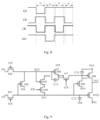
- FIG. 9 is a circuit diagram of the light-emitting control unit in the display device according to an embodiment of the present disclosure.
- FIG. 10 is an operation sequence diagram of the light-emitting control unit in FIG. 9 ;
- FIG. 11 is a circuit diagram of a pixel circuit in the display device according to an embodiment of the present disclosure.
- FIG. 12 is an operation sequence diagram of the pixel circuit in FIG. 11 .
- each transistor maybe a triode, a thin film transistor (TFT), a field effect transistor (FET), or any other element having a same characteristic.
- TFT thin film transistor
- FET field effect transistor
- each transistor may be called as a first electrode, and the other may be called as a second electrode.
- the control electrode when the transistor is a triode, the control electrode may be a base, the first electrode may be a collector and the second electrode may be an emitter, or the control electrode may be a base, the first electrode may be an emitter and the second electrode may be a collector.
- the control electrode when the transistor is a TFT or FET, the control electrode may be a gate electrode, the first electrode may be a drain electrode and the second electrode may be a source electrode, or the control electrode may be a gate electrode, the first electrode may be a source electrode and the second electrode may be a drain electrode.
- a main objective of the present disclosure is to provide a display driving module, a method for driving the display driving module and a display device, so as to address an issue that crosstalk occurs for pixel circuits in a previous row when charging pixel circuits in a row in the related art, resulting in overall crosstalk occurring for pixel circuits in multiple rows in a display screen.
- the display driving module is applied to the display device, the display device includes pixel circuits in multiple rows and multiple columns, and the display driving module includes a gate driving circuit, a plurality of data lines each extending in a column direction and a data driving circuit.
- the pixel circuits in odd-numbered rows and one column are electrically connected to a data line, and the pixel circuits in even-numbered rows and the one column are electrically connected to another data line.
- the data driving circuit includes a data driver DI and a multiplexing circuit
- the multiplexing circuit includes a first multiplexing sub-circuit 11 and a second multiplexing sub-circuit 12 .
- the first multiplexing sub-circuit 11 is electrically connected to a first multiplexing control terminal MUX 1 (as shown in FIG. 2 ), the data driver DI, the data lines (not shown in FIG. 1 ) electrically connected to the pixel circuits in odd-numbered rows and odd-numbered columns and the data lines (not shown in FIG. 1 ) electrically connected to the pixel circuits in even-numbered rows and even-numbered columns.
- the first multiplexing sub-circuit 11 is configured to control the data driver DI to apply corresponding data voltages to the data lines electrically connected to the pixel circuits in odd-numbered rows and odd-numbered columns and the data lines electrically connected to the pixel circuits in even-numbered rows and even-numbered columns under the control of a first multiplexing control signal from the first multiplexing control terminal MUX 1 .
- the second multiplexing sub-circuit 12 is electrically connected to a second multiplexing control terminal MUX 2 (as shown in FIG. 2 ), the data driver DI, the data lines (not shown in FIG. 1 ) electrically connected to the pixel circuits in odd-numbered rows and even-numbered columns and the data lines (not shown in FIG. 1 ) electrically connected to the pixel circuits in even-numbered rows and odd-numbered columns.
- the second multiplexing sub-circuit 12 is configured to control the data driver DI to apply corresponding data voltages to the data lines electrically connected to the pixel circuits in odd-numbered rows and even-numbered columns and the data lines electrically connected to the pixel circuits in even-numbered rows and odd-numbered columns under the control of a second multiplexing control signal from the second multiplexing control terminal MUX 2 .
- the gate driving circuit includes a plurality of levels of shift register units, an n th -level shift register unit is electrically connected to the pixel circuits in a (2n ⁇ 1) th row and a (2n) th row, and configured to apply a same gate driving signal to the pixel circuits in the (2n ⁇ 1) t row and the (2n) th row, wherein n is a positive integer.
- the shift register unit in the gate driving circuit is electrically connected to the pixel circuits in two rows, and configured to apply the same gate driving signal to the pixel circuits in two rows, so that charging times of the pixel circuits in two rows completely overlap.
- first multiplexing sub-circuit 11 is electrically connected to both the pixel circuits in odd-numbered rows and the pixel circuits in even-numbered rows
- second multiplexing sub-circuit 12 is electrically connected to both the pixel circuits in odd-numbered rows and the pixel circuits in even-numbered rows, so it is able to prevent crosstalk from occurring for the pixel circuits in a previous row when charging pixel circuits in a row, and prevent overall crosstalk from occurring for pixel circuits in multiple rows in the display screen.
- the shift register unit in the gate driving circuit does not apply an active gate driving signal, so it is able to avoid crosstalk caused by that, when a voltage on a data line jumps, it has a large influence on a potential at a node in the pixel circuit in the case that a data written-in transistor in a pixel circuit is turned on.
- the active first multiplexing control signal is referred to as a first multiplexing control signal through which it is able for the first multiplexing sub-circuit 11 to control the data driver DI to apply the corresponding data voltages to the data lines electrically connected to the pixel circuits in odd-numbered rows and odd-numbered columns and the data lines electrically connected to the pixel circuits in even-numbered rows and even-numbered columns.
- the active second multiplexing control signal is referred to as a second multiplexing control signal through which it is able for the second multiplexing sub-circuit 12 to control the data driver to apply the corresponding data voltages to the data lines electrically connected to the pixel circuits in odd-numbered rows and even-numbered columns and the data lines electrically connected to the pixel circuits in even-numbered rows and odd-numbered columns.
- the active gate driving signal is referred to as a gate driving signal through which it is able to control the data written-in transistor to be turned on.
- the pixel circuits are arranged in an active display region
- the n th -level shift register unit may include a first one of n th -level shift register modules located at a first side of the active display region, and a second one of n th -level shift register modules located at a second side of the active display region; the first side is opposite to the second side.
- the first side may be, but not limited to, a left side and the second side may be, but not limited to, a right side.
- the one-level shift register unit may include, but not limited to, two shift register modules applying the gate driving signal to the pixel circuits in one row simultaneously.
- the display driving module may include the plurality of data lines.
- the pixel circuits in odd-numbered rows and a (2m ⁇ 1) th column are electrically connected to a (4m ⁇ 3) th data line
- the pixel circuits in even-numbered rows and the (2m ⁇ 1) th column are electrically connected to a (4m ⁇ 2) th data line
- the pixel circuits in even-numbered rows and a (2m) th column are electrically connected to a (4m ⁇ 1) th data line
- the pixel circuits in odd-numbered rows and the (2m) th column are electrically connected to a (4m) th data line, where m is a positive integer.
- the first multiplexing sub-circuit 11 may be electrically connected to the (4m ⁇ 3) th data line and the (4m) th data line
- the second multiplexing sub-circuit 12 may be electrically connected to the (4m ⁇ 2) th data line and the (4m ⁇ 1) th data line.
- the first multiplexing sub-circuit may include at least one first multiplexing transistor and at least one second multiplexing transistor.
- a control electrode of the first multiplexing transistor is electrically connected to the first multiplexing control terminal, a first electrode of the first multiplexing transistor is electrically connected to the (4m ⁇ 3) th data line, and a second electrode of the first multiplexing transistor is electrically connected to the data driver.
- a control electrode of the second multiplexing transistor is electrically connected to the first multiplexing control terminal, a first electrode of the second multiplexing transistor is electrically connected to the (4m) th data line, and a second electrode of the second multiplexing transistor is electrically connected to the data driver.
- the first multiplexing transistor and the second multiplexing transistor are each an n-type transistor or a p-type transistor.
- the second multiplexing sub-circuit may include at least one third multiplexing transistor and at least one fourth multiplexing transistor.
- a control electrode of the third multiplexing transistor is electrically connected to the second multiplexing control terminal, a first electrode of the third multiplexing transistor is electrically connected to the (4m ⁇ 2) th data line, and a second electrode of the third multiplexing transistor is electrically connected to the data driver.
- a control electrode of the fourth multiplexing transistor is electrically connected to the second multiplexing control terminal, a first electrode of the fourth multiplexing transistor is electrically connected to the (4m ⁇ 1) th data line, and a second electrode of the fourth multiplexing transistor is electrically connected to the data driver.
- the third multiplexing transistor and the fourth multiplexing transistor are each an n-type transistor or a p-type transistor.
- the display device includes the display driving module and the pixel circuits in multiple rows located in the active display region 20 .
- the display driving module includes the gate driving circuit, the plurality of data lines each extending in the column direction and the data driving circuit.
- the pixel circuits in odd-numbered rows and one column are electrically connected to a data line, and the pixel circuits in even-numbered rows and the one column are electrically connected to another data line.
- the data driving circuit includes the data driver (DI) and the multiplexing circuit, and the multiplexing circuit includes the first multiplexing sub-circuit 11 and the second multiplexing sub-circuit 12 .
- FIG. 2 pixel circuits in a first row, a second row, a third row, a fourth row, a (2N ⁇ 3) th row, a (2N ⁇ 2) th row, a (2N ⁇ 1) th row and a (2N) th row located in the active display region 20 are shown (in FIG. 2 , the pixel circuits in the first row, the second row, the third row, the fourth row, the (2N ⁇ 3) th row, the (2N ⁇ 2) th row, the (2N ⁇ 1) th row and the (2N) th row are arranged sequentially along a direction from top to bottom), where N is an integer greater than 3.
- P 0 represents a pixel circuit.
- FIG. 2 shows a first one S 11 of first-level shift register modules and a second one S 12 of the first-level shift register modules in a first level shift register unit, a first one S 21 of second-level shift register modules and a second one S 22 of the second-level shift register modules in a second-level shift register unit, a first one SN 11 of (N ⁇ 1) th -level shift register modules and a second one SN 12 of the (N ⁇ 1) th -level shift register modules in a (N ⁇ 1) th -level shift register unit, a first one SN 1 of N th -level shift register modules and a second one SN 2 of the N th -level shift register modules in an N th -level shift register unit of the gate driving circuit.
- S 11 , S 21 , SN 11 and SN 1 are all arranged on the first side, such as the left side, of the active display region 20
- S 12 , S 22 , SN 12 and SN 2 are all arranged on the second side, such as the right side, of the active display region 20 .
- S 11 and S 12 each applies a first gate driving signal
- S 21 and S 22 each applies a second gate driving signal
- SN 11 and SN 12 each applies an (N ⁇ 1) th gate driving signal
- SN 1 and SN 2 each applies an (N) th gate driving signal
- Both S 11 and S 12 are electrically connected to the pixel circuits in the first row and the second row, and apply the first gate driving signal to the pixel circuits in the first row and the second row.
- Both S 21 and S 22 are electrically connected to the pixel circuits in the third row and the fourth row, and apply the second gate driving signal to the pixel circuits in the third row and the fourth row.
- Both SN 11 and SN 12 are electrically connected to the pixel circuits in the (2N ⁇ 3) th row and the (2N ⁇ 2) th row, and apply the (N ⁇ 1) th gate driving signal to the pixel circuits in the (2N ⁇ 3) th row and the (2N ⁇ 2) th row.
- Both SN 1 and SN 2 are electrically connected to the pixel circuits in the (2N ⁇ 1) th row and the (2N) th row, and apply the N th gate driving signal to the pixel circuits in the (2N ⁇ 1) th row and the (2N) th row.
- the pixel circuits in each column are electrically connected to two data lines.
- a first data line DL1 is electrically connected to the pixel circuits in odd-numbered rows and a first column
- a second data line DL2 is electrically connected to the pixel circuits in even-numbered rows and the first column.
- a third data line DL3 is electrically connected to the pixel circuits in even-numbered rows and a second column
- a fourth data line DL4 is electrically connected to the pixel circuits in odd-numbered rows and the second column.
- a (4M ⁇ 3) th data line DL4M ⁇ 3 is electrically connected to the pixel circuits in odd-numbered rows and a (2M ⁇ 1) th column
- a (4M ⁇ 2) th data line DL4M ⁇ 2 is electrically connected to the pixel circuits in even-numbered rows and the (2M ⁇ 1) th column
- a (4M ⁇ 1) th data line DL4M ⁇ 1 is electrically connected to the pixel circuits in even-numbered rows and a (2M) th column
- a (4M) th data line DL4M is electrically connected to the pixel circuits in odd-numbered rows and the (2M) th column.
- M is an integer greater than 1.
- FIG. 2 shows that the first multiplexing sub-circuit 11 includes a first one Tm 11 of first multiplexing transistors, a first one Tm 12 of second multiplexing transistors, an M th one TmM 1 of the first multiplexing transistors and an M th one TmM 2 of the second multiplexing transistors.
- a gate electrode of the Tm 11 is electrically connected to the first multiplexing control terminal MUX 1
- a drain electrode of the Tm 11 is electrically connected to the DL1
- a source electrode of the Tm 11 is electrically connected to the data driver DI.
- a gate electrode of the Tm 12 is electrically connected to the first multiplexing control terminal MUX 1 , a drain electrode of the Tm 12 is electrically connected to the DL4, and a source electrode of the Tm 12 is electrically connected to the data driver DI.
- a gate electrode of the TmM 1 is electrically connected to the first multiplexing control terminal MUX 1 , a drain electrode of the TmM 1 is electrically connected to the DL4M ⁇ 3, and a source electrode of the TmM 1 is electrically connected to the data driver DI.
- a gate electrode of the TmM 2 is electrically connected to the first multiplexing control terminal MUX 1 , a drain electrode of TmM 2 is electrically connected to DL4M, and a source electrode of the TmM 2 is electrically connected to the data driver DI.
- FIG. 2 shows that the second multiplexing sub-circuit 12 includes a first one Tm 13 of third multiplexing transistors, a first one Tm 14 of fourth multiplexing transistors, an M th one TmM 3 of the third multiplexing transistors and an M th one TmM 4 of the fourth multiplexing transistors.
- a gate electrode of the Tm 13 is electrically connected to the second multiplexing control terminal MUX 2
- a drain electrode of the Tm 13 is electrically connected to the DL2
- a source electrode of the Tm 13 is electrically connected to the data driver DI.
- a gate electrode of the Tm 14 is electrically connected to the second multiplexing control terminal MUX 2 , a drain electrode of the Tm 14 is electrically connected to the DL3, and a source electrode of the Tm 14 is electrically connected to the data driver DI.
- a gate electrode of the TmM 3 is electrically connected to the second multiplexing control terminal MUX 2 , a drain electrode of the TmM 3 is electrically connected to the DL4m ⁇ 2, and a source electrode of the TmM 3 is electrically connected to the data driver DI.
- a gate electrode of the TmM 4 is electrically connected to the second multiplexing control terminal MUX 2 , a drain electrode of TmM 4 is electrically connected to DL4m ⁇ 1, and a source electrode of the TmM 4 is electrically connected to the data driver DI.
- all multiplexing transistors are, but not limited to, p-type thin film transistors.
- 10 denotes a display substrate in the display device, and the pixel circuits and the display driving module may be arranged on the display substrate 10 .
- each data line extracted from the data driver DI longitudinally passes through corresponding pixel circuits, and the pixel circuits in each column is controlled to emit light by two data lines.
- a gate line electrically connected to the gate driving circuit and a light-emitting control line electrically connected to the light-emitting control circuit pass through the pixel circuits in a corresponding row.
- the MUX 1 applies a low voltage signal
- each multiplexing transistor in the first multiplexing sub-circuit 11 is controlled to be turned on, so that the DI applies the corresponding data voltages to the pixel circuits in odd-numbered rows and odd-numbered columns and the pixel circuits in odd-numbered rows and even-numbered columns.
- the MUX 2 applies a low voltage signal
- each multiplexing transistor in the second multiplexing sub-circuit 12 is controlled to be turned on, so that the DI applies the corresponding data voltages to the pixel circuits in even-numbered rows and odd-numbered columns and the pixel circuits in even-numbered rows and even-numbered columns.
- the (N ⁇ 1) th gate driving signal (GN ⁇ 1) applied to the pixel circuits in the (2N ⁇ 3) th row and the pixel circuits in the (2N ⁇ 2) th row by the SN 11 and the SN 12 is a low voltage signal, so as to enable data written-in transistors of the pixel circuits in the (2N ⁇ 3) th row and the (2N ⁇ 2) th row to be turned on, thereby to charge the corresponding pixel circuits via the corresponding data lines respectively.
- the MUX 1 applies a low voltage signal, each multiplexing transistor in the first multiplexing sub-circuit 11 is controlled to be turned on, so that the DI applies the corresponding data voltages to the pixel circuits in odd-numbered rows and odd-numbered columns and the pixel circuits in odd-numbered rows and even-numbered columns.
- the MUX 2 applies a low voltage signal, each multiplexing transistor in the second multiplexing sub-circuit 12 is controlled to be turned on, so that the DI applies the corresponding data voltages to the pixel circuits in even-numbered rows and odd-numbered columns and the pixel circuits in even-numbered rows and even-numbered columns.
- the N th gate driving signal GN applied to the pixel circuits in the (2N ⁇ 1) th row and the (2N) th row is a low voltage signal, so as to enable data written-in transistors of the pixel circuits in the (2N ⁇ 1) th row and the (2N) th row to be turned on, thereby to charge the corresponding pixel circuits via the corresponding column data lines respectively.
- the time for charging the pixel circuits in each row is greater than TH, it is sufficient to perform charging in the case of high frequency frames, and eliminate crosstalk for data in adjacent rows.
- TH is a display time of the pixel circuits in one row. For example, when there are pixel circuits in 2N rows in a display device and a screen refresh rate is 120 Hz, TH is equal to 1 ⁇ 2N/120.
- some direct current signal lines including a first driving voltage signal ELVDD and a second driving voltage signal ELVSS and an initial voltage signal of an Organic Light Emitting Diode (OLED), in the display device are not shown in FIGS. 2 and 4 , and distributed over each pixel circuit.
- ELVDD first driving voltage signal
- ELVSS second driving voltage signal
- OLED Organic Light Emitting Diode
- CK denotes the first clock signal terminal
- CB denotes the second clock signal terminal
- CK and CB apply clock signals to each level of the shift register unit.
- each level shift register unit in the gate driving circuit does not output a low voltage signal, so it is able to control a data written-in transistor in a pixel circuit not to be turned on when a voltage on a data line jumps, thereby to prevent a display from being adversely affected by a change in the voltage on the data line, and avoid crosstalk.
- the display driving module may include the plurality of data lines, the pixel circuits in even-numbered rows and a (2m ⁇ 1) th column are electrically connected to a (4m ⁇ 3) th data line, the pixel circuits in odd-numbered rows and the (2m ⁇ 1) th column are electrically connected to a (4m ⁇ 2) th data line, the pixel circuits in even-numbered rows and a (2m) th column are electrically connected to a (4m ⁇ 1) th data line, the pixel circuits in odd-numbered rows and the (2m) th column are electrically connected to a (4m) th data line, where m is a positive integer.
- the first multiplexing sub-circuit 11 may be electrically connected to the (4m ⁇ 2) th data line and the (4m ⁇ 1) th data line
- the second multiplexing sub-circuit 12 may be electrically connected to the (4m ⁇ 3) th data line and the (4m) th data line.
- the second multiplexing sub-circuit may include at least one third multiplexing transistor and at least one fourth multiplexing transistor.
- a control electrode of the first multiplexing transistor is electrically connected to the first multiplexing control terminal, a first electrode of the first multiplexing transistor is electrically connected to the (4m ⁇ 2) th data line, and a second electrode of the first multiplexing transistor is electrically connected to the data driver.
- a control electrode of the second multiplexing transistor is electrically connected to the first multiplexing control terminal, a first electrode of the second multiplexing transistor is electrically connected to the (4m ⁇ 1) th data line, and a second electrode of the second multiplexing transistor is electrically connected to the data driver.
- the first multiplexing transistor and the second multiplexing transistor are each an n-type transistor or a p-type transistor.
- the second multiplexing sub-circuit may include at least at least one third multiplexing transistor and at least one fourth multiplexing transistor.
- a control electrode of the third multiplexing transistor is electrically connected to the second multiplexing control terminal, a first electrode of the third multiplexing transistor is electrically connected to the (4m ⁇ 3) th data line, and a second electrode of the third multiplexing transistor is electrically connected to the data driver.
- a control electrode of the fourth multiplexing transistor is electrically connected to the second multiplexing control terminal, a first electrode of the fourth multiplexing transistor is electrically connected to the (4m) th data line, and a second electrode of the fourth multiplexing transistor is electrically connected to the data driver.
- the first multiplexing transistor and the second multiplexing transistor are each an n-type transistor or a p-type transistor.
- the display device includes the display driving module and the pixel circuits in multiple rows located in the active display region 20 .
- the display driving module includes the gate driving circuit, the plurality of data lines each extending in the column direction and the data driving circuit.
- the pixel circuits in odd-numbered rows and one column are electrically connected to a data line, and the pixel circuits in even-numbered rows and the one column are electrically connected to another data line.
- the data driving circuit includes the data driver DI and the multiplexing circuit 21
- the multiplexing circuit 21 includes the first multiplexing sub-circuit 11 and the second multiplexing sub-circuit 12 .
- FIG. 4 pixel circuits in a first row, a second row, a third row, a fourth row, a (2N ⁇ 3) th row, a (2N ⁇ 2) th row, a (2N ⁇ 1) th row and a (2N) th row located in the active display region 20 are shown (in FIG. 4 , the pixel circuits in the first row, the second row, the third row, the fourth row, the (2N ⁇ 3) th row, the (2N ⁇ 2) th row, the (2N ⁇ 1) th row and the (2N) th row are arranged sequentially along a direction from top to bottom), where N is an integer greater than 3.
- P 0 represents a pixel circuit
- FIG. 4 shows a first one S 11 of first-level shift register modules and a second one S 12 of the first-level shift register modules in a first level shift register unit, a first one S 21 of second-level shift register modules and a second one S 22 of the second-level shift register modules in a second-level shift register unit, a first one SN 11 of (N ⁇ 1) th -level shift register modules and a second one SN 12 of the (N ⁇ 1) th -level shift register modules in a (N ⁇ 1) th -level shift register unit, a first one SN 1 of N th -level shift register modules and a second one SN 2 of the N th -level shift register modules in an N th -level shift register unit of the gate driving circuit.
- S 11 , S 21 , SN 11 and SN 1 are all arranged on the first side, such as the left side, of the active display region 20
- S 12 , S 22 , SN 12 and SN 2 are all arranged on the second side, such as the right side, of the active display region 20 .
- S 11 and S 12 each applies a first gate driving signal
- S 21 and S 22 each applies a second gate driving signal
- SN 11 and SN 12 each applies an (N ⁇ 1) th gate driving signal
- SN 1 and SN 2 each applies an (N) th gate driving signal
- Both S 11 and S 12 are electrically connected to the pixel circuits in the first row and the second row, and apply the first gate driving signal to the pixel circuits in the first row and the second row.
- Both S 21 and S 22 are electrically connected to the pixel circuits in the third row and the fourth row, and apply the second gate driving signal to the pixel circuits in the third row and the fourth row.
- Both SN 11 and SN 12 are electrically connected to the pixel circuits in the (2N ⁇ 3) th row and the (2N ⁇ 2) th row, and apply the (N ⁇ 1) th gate driving signal to the pixel circuits in the (2N ⁇ 3) th row and the (2N ⁇ 2) th row.
- Both SN 1 and SN 2 are electrically connected to the pixel circuits in the (2N ⁇ 1) th row and the (2N) th row, and apply the N th gate driving signal to the pixel circuits in the (2N ⁇ 1) th row and the (2N) th row.
- the pixel circuits in each column are electrically connected to two data lines.
- a first data line DL1 is electrically connected to the pixel circuits in even-numbered rows and a first column
- a second data line DL2 is electrically connected to the pixel circuits in odd-numbered rows and the first column.
- a third data line DL3 is electrically connected to the pixel circuits in even-numbered rows and a second column
- a fourth data line DL4 is electrically connected to the pixel circuits in odd-numbered rows and the second column.
- a (4M ⁇ 3) th data line DL4M ⁇ 3 is electrically connected to the pixel circuits in even-numbered rows and a (2M ⁇ 1) th column
- a (4M ⁇ 2) th data line DL4M ⁇ 2 is electrically connected to the pixel circuits in odd-numbered rows and the (2M ⁇ 1) th column.
- a (4M ⁇ 1) th data line DL4M ⁇ 1 is electrically connected to the pixel circuits in even-numbered rows and a (2M) th column
- a (4M) th data line DL4M is electrically connected to the pixel circuits in odd-numbered rows and the (2M) th column.
- M is an integer greater than 1.
- FIG. 4 shows that the first multiplexing sub-circuit 11 includes a first one Tm 11 of first multiplexing transistors, a first one Tm 12 of second multiplexing transistors, an M th one TmM 1 of the first multiplexing transistors and an M th one TmM 2 of the second multiplexing transistors.
- a gate electrode of the Tm 11 is electrically connected to the first multiplexing control terminal MUX 1 , a drain electrode of the Tm 11 is electrically connected to the DL2, and a source electrode of the Tm 11 is electrically connected to the data driver DI.
- a gate electrode of the Tm 12 is electrically connected to the first multiplexing control terminal MUX 1 , a drain electrode of the Tm 12 is electrically connected to the DL3, and a source electrode of the Tm 12 is electrically connected to the data driver DI.
- a gate electrode of the TmM 1 is electrically connected to the first multiplexing control terminal MUX 1 , a drain electrode of the TmM 1 is electrically connected to the DL4M ⁇ 2, and a source electrode of the TmM 1 is electrically connected to the data driver DI.
- a gate electrode of the TmM 2 is electrically connected to the first multiplexing control terminal MUX 1 , a drain electrode of TmM 2 is electrically connected to DL4M ⁇ 1, and a source electrode of the TmM 2 is electrically connected to the data driver DI.
- FIG. 4 shows that the second multiplexing sub-circuit 12 includes a first one Tm 13 of third multiplexing transistors, a first one Tm 14 of fourth multiplexing transistors, an M th one TmM 3 of the third multiplexing transistors and an M th one TmM 4 of the fourth multiplexing transistors.
- a gate electrode of the Tm 13 is electrically connected to the second multiplexing control terminal MUX 2 , a drain electrode of the Tm 13 is electrically connected to the DL1, and a source electrode of the Tm 13 is electrically connected to the data driver DI.
- a gate electrode of the Tm 14 is electrically connected to the second multiplexing control terminal MUX 2 , a drain electrode of the Tm 14 is electrically connected to the DL4, and a source electrode of the Tm 14 is electrically connected to the data driver DI.
- a gate electrode of the TmM 3 is electrically connected to the second multiplexing control terminal MUX 2 , a drain electrode of the TmM 3 is electrically connected to the DL4m ⁇ 3, and a source electrode of the TmM 3 is electrically connected to the data driver DI.
- a gate electrode of the TmM 4 is electrically connected to the second multiplexing control terminal MUX 2 , a drain electrode of TmM 4 is electrically connected to DL4m, and a source electrode of the TmM 4 is electrically connected to the data driver DI.
- all multiplexing transistors are, but not limited to, p-type thin film transistors.
- 10 denotes a display substrate included in a display device, and the pixel circuits and the display driving module may be arranged on the display substrate 10 .
- the MUX 1 applies a low voltage signal
- each multiplexing transistor in the first multiplexing sub-circuit 11 is controlled to be turned on, so that the DI applies the corresponding data voltages to the pixel circuits in odd-numbered rows and odd-numbered columns and the pixel circuits in even-numbered rows and even-numbered columns.
- the MUX 2 applies a low voltage signal
- each multiplexing transistor in the second multiplexing sub-circuit 12 is controlled to be turned on, so that the DI applies the corresponding data voltages to the pixel circuits in odd-numbered rows and even-numbered columns and the pixel circuits in even-numbered rows and odd-numbered columns.
- the (N ⁇ 1) th gate driving signal (GN ⁇ 1) applied to the pixel circuits in the (2N ⁇ 3) th row and the (2N ⁇ 2) th row by the SN 11 and the SN 12 is a low voltage signal, so as to enable data written-in transistors of the pixel circuits in the (2N ⁇ 3) th row and the (2N ⁇ 2) th row to be turned on, thereby to charge the corresponding pixel circuits via the corresponding data lines respectively.
- the MUX 1 applies a low voltage signal, each multiplexing transistor in the first multiplexing sub-circuit 11 is controlled to be turned on, so that the DI applies the corresponding data voltages to the pixel circuits in odd-numbered rows and odd-numbered columns and the pixel circuits in even-numbered rows and even-numbered columns.
- the MUX 2 applies a low voltage signal, each multiplexing transistor in the second multiplexing sub-circuit 12 is controlled to be turned on, so that the DI applies the corresponding data voltages to the pixel circuits in odd-numbered rows and even-numbered columns and the pixel circuits in even-numbered rows and odd-numbered columns.
- the N th gate driving signal GN applied to the pixel circuits in the (2N ⁇ 1) th row and the (2N) th row is a low voltage signal, so as to enable data written-in transistors of the pixel circuits in the (2N ⁇ 1) th row and the (2N) th row to be turned on, thereby to charge the corresponding pixel circuits via the corresponding column data lines respectively.
- the display driving module may further include a light-emitting control circuit, the light-emitting control circuit includes a plurality of levels of light-emitting control units, and an n th -level light-emitting control unit is electrically connected to the pixel circuits in the (2n ⁇ 1) th row and the (2n) th row, and configured to apply a same light-emitting control signal to the pixel circuits in the (2n ⁇ 1) th row and the (2n) th row, where n is a positive integer.
- the light-emitting control circuit includes a plurality of levels of light-emitting control units, and an n th -level light-emitting control unit is electrically connected to the pixel circuits in the (2n ⁇ 1) th row and the (2n) th row, and configured to apply a same light-emitting control signal to the pixel circuits in the (2n ⁇ 1) th row and the (2n) th row, where n is a positive integer.
- the display driving module may further include the light-emitting control circuit, and the light-emitting control units in the light-emitting control circuit apply the same light-emitting control signal to the pixel circuits in two adjacent rows.
- the n th -level light-emitting control unit may include a first one of n th -level light-emitting control modules and a second one of the n th -level light-emitting control modules, the first one of the n th -level light-emitting control modules is arranged on the first side, such as the left side, of the active display region, the second one of the n th -level light-emitting control modules is arranged on the second side, such as the right side, of the active display region, and the first one of the n th -level light-emitting control modules and the second one of the n th -level light-emitting control modules apply light-emitting control signals to the pixel circuits in the (2n ⁇ 1) th row and the (2n) th row simultaneously.
- E 11 is electrically connected to the pixel circuits in the first row and the second row
- E 12 is electrically connected to the pixel circuits in the first row and the second row.
- E 21 is electrically connected to the pixel circuits in the third row and the fourth row
- E 22 is electrically connected to the pixel circuits in the third row and the fourth row.
- EN 11 is electrically connected to the pixel circuits in the (2N ⁇ 3) th row and the (2N ⁇ 2) th row
- EN 12 is electrically connected to the pixel circuits in the (2N ⁇ 3) th row and the (2N ⁇ 2) th row.
- EN 1 is electrically connected to the pixel circuits in the (2N ⁇ 1) th row and the (2N) th row
- EN 2 is electrically connected to the pixel circuits in the (2N ⁇ 1) th row and the (2N) th row.
- the n th -level shift register unit may include an n th -level pull-up node control circuit 51 , an n th -level pull-down control node control circuit 52 , an n th -level pull-down node control circuit 53 and an n th -level gate driving signal output circuit 54 .
- the n th -level pull-up node control circuit 51 is electrically connected to a first clock signal terminal CK, a first voltage terminal V 1 , an n th -level pull-up node N 2 and an n th -level pull-down control node N 1 , and configured to control the n th -level pull-up node N 2 to be electrically connected to the first voltage terminal V 1 under the control of a first clock signal from the first clock signal terminal CK, and control the n th -level pull-up node N 2 to be electrically connected to the first clock signal terminal CK and maintain a potential at the n th -level pull-up node N 2 under the control of a potential at the n th -level pull-down control node N 1 .
- the n th -level pull-down control node control circuit 52 is electrically connected to an input terminal GI, the first clock signal terminal CK, a second clock signal terminal CB, the n th -level pull-up node N 2 , a second voltage terminal V 2 and the n th -level pull-down control node N 1 , and configured to control the n th -level pull-down control node N 1 to be electrically connected to the input terminal GI under the control of the first clock signal, control the n th -level pull-down control node N 1 to be electrically connected to the second voltage terminal V 2 under the control of the potential at the n th -level pull-up node N 2 and a second clock signal from the second clock signal terminal CB.
- the n th -level pull-down node control circuit 53 is electrically connected to the n th -level pull-down control node N 1 , the first voltage terminal V 1 and the n th -level pull-down node N 4 , and configured to control the n th -level pull-down control node N 1 to be electrically connected to the n th -level pull-down node N 4 and maintain a potential at the n th -level pull-down node N 4 under the control of a first voltage signal from the first voltage terminal V 1 .
- the n th -level gate driving signal output circuit 54 is electrically connected to the n th -level pull-up node N 2 , the n th -level pull-down node N 4 , the second voltage terminal V 2 , the second clock signal terminal CB and an n th -level gate driving signal output terminal GO, and configured to control the n th -level gate driving signal output terminal GO to be electrically connected to the second voltage terminal V 2 under the control of the potential at the n th -level pull-up node N 2 , and control the n th -level gate driving signal output terminal GO to be electrically connected to the second clock signal terminal CB under the control of the potential at the n th -level pull-down node N 4 .
- the n th -level gate driving signal output terminal GO is electrically connected to the pixel circuits (not shown in FIG. 6 ) in the (2n ⁇ 1) th row and the (2n) th row.
- the n th -level pull-up node control circuit 51 controls the potential at the n th -level pull-up node N 2
- the n th -level pull-down control node control circuit 52 controls the potential at the n th -level pull-down control node N 1
- the n th -level pull-down node control circuit 53 controls the potential at the n th -level pull-down node
- the n th -level gate driving signal output circuit 54 is configured to control the n th -level gate driving signal output terminal GO to output an n th -level gate driving signal.
- the n th -level pull-up node control circuit may include a first scanning control transistor, a second scanning control transistor and a first scanning storage capacitor.
- a control electrode of the first scanning control transistor is electrically connected to the first clock signal terminal, a first electrode of the first scanning control transistor is electrically connected to the first voltage terminal, and a second electrode of the first scanning control transistor is electrically connected to the n th -level pull-up node.
- a control electrode of the second scanning control transistor is electrically connected to the n th -level pull-down control node, a first electrode of the second scanning control transistor is electrically connected to the n th -level pull-up node, and a second electrode of the second scanning control transistor is electrically connected to the first clock signal terminal.
- a first terminal of the first scanning storage capacitor is electrically connected to the n th -level pull-up node, and a second terminal of the first scanning storage capacitor is electrically connected to the second voltage terminal.
- the n th -level pull-down control node control circuit may include a third scanning control transistor, a fourth scanning control transistor and a fifth scanning control transistor.
- a control electrode of the third scanning control transistor is electrically connected to the first clock signal terminal, a first electrode of the third scanning control transistor is electrically connected to the input terminal, and a second electrode of the third scanning control transistor is electrically connected to the n th -level pull-down control node.
- a control electrode of the fourth scanning control transistor is electrically connected to the n th -level pull-up node, and a first electrode of the fourth scanning control transistor is electrically connected to the second voltage terminal.
- a control electrode of the fifth scanning control transistor is electrically connected to the second clock signal terminal, a first electrode of the fifth scanning control transistor is electrically connected to a second electrode of the fourth scanning control transistor, and a second electrode of the fifth scanning control transistor is electrically connected to the n th -level pull-down control node.
- the n th -level pull-down node control circuit may include a sixth scanning control transistor and a second scanning storage capacitor.
- a control electrode of the sixth scanning control transistor is electrically connected to the first voltage terminal, a first electrode of the sixth scanning control transistor is electrically connected to the n th -level pull-down control node, and a second electrode of the sixth scanning control transistor is electrically connected to the n th -level pull-down node.
- a first terminal of the second scanning storage capacitor is electrically connected to the n th -level pull-down node, and a second terminal of the second scanning storage capacitor is electrically connected to the n th -level gate driving signal output terminal.
- the n th -level gate driving signal output circuit may include a seventh scanning control transistor and an eighth scanning control transistor.
- a control electrode of the seventh scanning control transistor is electrically connected to the n th -level pull-up node, a first electrode of the seventh scanning control transistor is electrically connected to the second voltage terminal, and a second electrode of the seventh scanning control transistor is electrically connected to the n th -level gate driving signal output terminal.
- a control electrode of the eighth scanning control transistor is electrically connected to the n th -level pull-down node, a first electrode of the eighth scanning control transistor is electrically connected to the n th -level gate driving signal output terminal, and a second electrode of the eighth scanning control transistor is electrically connected to the second clock signal terminal.
- the n th -level pull-up node control circuit may include a first scanning control transistor T 3 , a second scanning control transistor T 2 and a first scanning storage capacitor C 2 .
- a gate electrode of the first scanning control transistor T 3 is electrically connected to the first clock signal terminal CK, a source electrode of the first scanning control transistor T 3 receives a first low voltage VL, and a drain electrode of the first scanning control transistor T 3 is electrically connected to the n th -level pull-up node N 2 .
- a gate electrode of the second scanning control transistor T 2 is electrically connected to the n th -level pull-down control node N 1 , a source electrode of the second scanning control transistor T 2 is electrically connected to the n th -level pull-up node N 2 , and a drain electrode of the second scanning control transistor T 2 is electrically connected to the first clock signal terminal CK.
- a first terminal of the first scanning storage capacitor C 2 is electrically connected to the n th -level pull-up node N 2 , and a second terminal of the first scanning storage capacitor C 2 receives a first high voltage VH.
- the n th -level pull-down control node control circuit may include a third scanning control transistor T 1 , a fourth scanning control transistor T 6 and a fifth scanning control transistor T 7 .
- a gate electrode of the third scanning control transistor T 1 is electrically connected to the first clock signal terminal CK, a source electrode of the third scanning control transistor T 1 is electrically connected to the input terminal GI, and a drain electrode of the third scanning control transistor T 1 is electrically connected to the n th -level pull-down control node N 1 .
- a gate electrode of the fourth scanning control transistor T 6 is electrically connected to the n th -level pull-up node N 2 , and a source electrode of the fourth scanning control transistor T 6 receives the first high voltage VH.
- a gate electrode of the fifth scanning control transistor T 7 is electrically connected to the second clock signal terminal CB, a source electrode of the fifth scanning control transistor T 7 is electrically connected to a drain electrode of the fourth scanning control transistor T 6 , and a drain electrode of the fifth scanning control transistor T 7 is electrically connected to the n th -level pull-down control node N 1 .
- the n th -level pull-down node control circuit may include a sixth scanning control transistor T 8 and a second scanning storage capacitor C 1 .
- a gate electrode of the sixth scanning control transistor T 8 receives the first low voltage, a source electrode of the sixth scanning control transistor T 8 is electrically connected to the n th -level pull-down control node N 1 , and a drain electrode of the sixth scanning control transistor T 8 is electrically connected to the n th -level pull-down node N 4 .
- a first terminal of the second scanning storage capacitor C 1 is electrically connected to the n th -level pull-down node N 4 , and a second terminal of the second scanning storage capacitor C 1 is electrically connected to the n th -level gate electrode driving signal output terminal GO.
- the n th -level gate driving signal output circuit may include a seventh scanning control transistor T 4 and an eighth scanning control transistor T 5 .
- a gate electrode of the seventh scanning control transistor T 4 is electrically connected to the n th -level pull-up node N 2 , a source electrode of the seventh scanning control transistor T 4 receives the first high voltage VH, and a drain electrode of the seventh scanning control transistor T 4 is electrically connected to the n th -level gate electrode driving signal output terminal GO.
- a gate electrode of the eighth scanning control transistor T 5 is electrically connected to the n th -level pull-down node N 4 , a source electrode of the eighth scanning control transistor T 5 is electrically connected to the n th -level gate electrode driving signal output terminal GO, and a source electrode of the eighth scanning control transistor T 5 is electrically connected to the second clock signal terminal CB.
- all transistors are, but not limited to, p-type thin film transistors.
- the gate driving circuit needs to output a low potential pulse signal in a row-by-row manner, as a result, some basic control signals, including the first high voltage VH, the first low voltage VL, the first clock signal and the second clock signal, are introduced into the gate driving circuit.
- some basic control signals including the first high voltage VH, the first low voltage VL, the first clock signal and the second clock signal.
- GI applies a low voltage signal (a gate signal output terminal of the (n ⁇ 1) th -level shift register unit is electrically connected to an input terminal GI of the n th -level shift register unit), the first clock signal from the CK is a low voltage signal, the second clock signal from the CB is a high voltage signal, T 1 , T 2 , T 3 , T 4 , T 5 , T 6 and T 8 are all turned on, and the GO outputs a high voltage signal.
- GI applies a high voltage signal
- the first clock signal from the CK is a high voltage signal
- the second clock signal from the CB is a low voltage signal
- T 2 , T 5 and T 7 are all turned on, and the GO outputs a low voltage signal.
- GI applies a high voltage signal
- the first clock signal from the CK is a low voltage signal
- the second clock signal from the CB is a high voltage signal
- T 1 , T 3 , T 4 , T 6 and T 8 are turned on, and the GO outputs a high voltage signal.
- GI applies a high voltage signal
- the first clock signal from the CK is a high voltage signal
- the second clock signal from the CB is a low voltage signal
- T 4 , T 6 , T 7 and T 8 are turned on, and the GO outputs a high voltage signal.
- potentials at internal nodes of the n th -level shift register unit may be switched between two stages of t 3 and t 4 until that the input signal from the GI is a low voltage signal during a display time of a next frame, and the stage of t 1 is entered again.
- the light-emitting control unit may include a first transistor M 1 , a second transistor M 2 , a third transistor M 3 , a fourth transistor M 4 , a fifth transistor M 5 , a sixth transistor M 6 , a seventh transistor M 7 , an eighth transistor M 8 , a ninth transistor M 9 , a tenth transistor M 10 , a first light-emitting control capacitor C 11 , a second light-emitting control capacitor C 12 and a third light-emitting control capacitor C 13 .
- a gate electrode of the M 1 is electrically connected to a third clock signal terminal ECK, a source electrode of the M 1 is electrically connected to a start signal terminal STV, and a drain electrode of the M 1 is electrically connected to a first node N 11 .
- a gate electrode of the M 2 is electrically connected to the first node N 11 , a source electrode of the M 2 is electrically connected to the third clock signal terminal ECK, and a drain electrode of the M 2 is electrically connected to a second node N 12 .
- a gate electrode of the M 3 is electrically connected to the third clock signal terminal ECK, a source electrode of the M 3 is connected to a second low voltage VGL, and a drain electrode of the M 3 is electrically connected to the second node N 12 .
- a gate electrode of the M 4 is electrically connected to a fourth clock signal terminal ECB, and a source electrode of the M 4 is electrically connected to the first node N 11 .
- a gate electrode of the M 5 is electrically connected to the second node N 12 , a source electrode of the M 5 receives a second high voltage VGH, and a drain electrode of M 5 is electrically connected to a drain electrode of the M 4 .
- a gate electrode of the M 6 is electrically connected to the second node N 12 , a source electrode of the M 6 is electrically connected to the fourth clock signal terminal ECB, and a drain electrode of the M 6 is electrically connected to a third node N 13 .
- a gate electrode of the M 7 is electrically connected to the fourth clock signal terminal ECB, a source electrode of the M 7 is connected to the third node N 13 , and a drain electrode of the M 7 is electrically connected to a fourth node N 14 .
- a gate electrode of the M 8 is electrically connected to the first node N 11 , a source electrode of the M 8 receives the second high voltage VGH, and a drain electrode of the M 8 is electrically connected to the fourth node N 14 .
- a gate electrode of the M 9 is electrically connected to the fourth node N 14 , a source electrode of the M 9 receives the second high voltage VGH, and a drain electrode of the M 9 is electrically connected to a light-emitting control signal output terminal OUT.
- a gate electrode of the M 10 is electrically connected to the first node N 11 , a source electrode of the M 10 receives the second low voltage VGL, and a drain electrode of the M 10 is electrically connected to the light-emitting control signal output terminal OUT.
- a first terminal of the C 11 is electrically connected to the second node N 12
- a second terminal of the C 11 is electrically connected to the third node N 13 .
- a first terminal of the C 12 is electrically connected to the first node N 11 , and a second terminal of the C 12 is electrically connected to the fourth clock signal terminal ECB.
- a first terminal of the C 13 is electrically connected to the fourth node N 14 , and a second terminal of the C 13 receives the second high voltage VGH.
- each transistor is, but not limited to, a p-type thin film transistor.
- FIG. 10 is an operation sequence diagram of the light-emitting control unit in FIG. 9 .
- OUT NEXT is a light-emitting control signal terminal of a next-level light-emitting control terminal unit.
- FIG. 11 is a circuit diagram of a pixel circuit in the display device according to an embodiment of the present disclosure.
- the pixel circuit in FIG. 11 is of a 7T1C structure which is a mainstream structure in the current OLED (Organic Light Emitting Diode) display product.
- OLED Organic Light Emitting Diode
- T 12 and T 14 are electrically connected to a current gate line, and the current gate line is electrically connected to a corresponding level shift register unit in the gate driving circuit.
- T 11 and T 17 are electrically connected to a previous gate line, and the previous gate line is electrically connected to a previous-level shift register unit in the gate driving circuit.
- T 15 and T 16 are electrically connected to a light-emitting control line in a current row, and the light-emitting control line in the current row is electrically connected to a corresponding level light-emitting control unit in the light-emitting control circuit.
- T 12 , T 14 , T 11 , T 17 , T 15 and T 16 are each used as a switch, T 13 is controlled by a data voltage signal, and T 13 drives an OLED to emit light.
- each pixel circuit may include a first pixel transistor T 11 , a second pixel transistor T 12 , a third pixel transistor T 13 , a fourth pixel transistor T 14 , a fifth pixel transistor T 15 , a sixth pixel transistor T 16 , a seventh pixel transistor T 17 , a storage capacitor Cst and an organic light-emitting diode (OLED).
- a first pixel transistor T 11 a second pixel transistor T 12
- a third pixel transistor T 13 a fourth pixel transistor T 14
- a fifth pixel transistor T 15 a sixth pixel transistor T 16
- a seventh pixel transistor T 17 a storage capacitor Cst and an organic light-emitting diode (OLED).
- OLED organic light-emitting diode
- C_Data denotes a parasitic capacitance on a data line Data.
- a gate electrode of the T 11 is electrically connected to a previous gate line Gs, a source electrode of the T 11 is connected to an initial voltage signal Vinit, and a drain electrode of the T 11 is electrically connected to a first control node J 1 .
- a gate electrode of the T 12 is electrically connected to a current gate line Gate, a source electrode of the T 12 is electrically connected to the first control node J 1 , and a drain electrode of the T 12 is electrically connected to a third control node J 3 .
- a gate electrode of the T 13 is electrically connected to the first control node J 1 , a source electrode of the T 13 is electrically connected to a second control node J 2 , and a drain electrode of the T 13 is electrically connected to the third control node J 3 .
- a gate electrode of the T 14 is electrically connected to the current gate line Gate, a source electrode of the T 14 is electrically connected to the second control node J 2 , and a drain electrode of the T 14 is electrically connected to the data line Data.
- a gate electrode of the T 15 is electrically connected to a light-emitting control line EM in a current row, a source electrode of the T 15 is connected to a first driving voltage signal ELVDD, and a drain electrode of the T 15 is electrically connected to the second control node J 2 .
- a gate electrode of the T 16 is electrically connected to the light-emitting control line EM in the current row, a source electrode of the T 16 is electrically connected to the third control node J 3 , and a drain electrode of the T 16 is electrically connected to a fourth control node J 4 .
- a gate electrode of the T 17 is electrically connected to the previous gate line Gs, a source electrode of the T 17 is connected to the initial voltage signal Vinit, and a drain electrode of the T 17 is electrically connected to the fourth control node J 4 .
- An anode of OLED is electrically connected to the fourth control node J 4 , and a cathode of OLED is connected to a second driving voltage signal ELVSS.
- each transistor is, but not limited to, a p-type thin film transistor.
- FIG. 12 is an operation sequence diagram of the pixel circuit in FIG. 11 .
- EM applies a low voltage signal
- Gate applies a high voltage signal
- the pixel circuit emits light in accordance with a data voltage signal being written-in previously.
- EM applies a high voltage signal
- Gs applies a low voltage signal
- T 15 and T 16 are turned off
- both T 11 and T 17 are turned on
- a potential at J 1 is reset to Vinit
- a potential at J 4 is set to Vinit.
- Gs applies a high voltage signal
- Gate applies a low voltage signal
- EM applies a high voltage signal
- T 11 is turned off
- T 12 and T 14 are turned on
- the Cst is charged through a data voltage Vdata from the Data until the potential at J 1 becomes Vdata-Vth, where Vth is a threshold voltage of T 3 .
- Gs applies a high voltage signal
- Gate applies a high voltage signal
- EM applies a low voltage signal
- T 5 and T 6 are turned on
- T 3 drives the OLED to emit light until t 21 in a display time of a next frame arrives.
- the method for driving the above-mentioned display driving module includes: controlling, by the first multiplexing sub-circuit, the data driver to apply corresponding data voltages to the data lines electrically connected to the pixel circuits in odd-numbered rows and odd-numbered columns and the data lines electrically connected to the pixel circuits in even-numbered rows and even-numbered columns under the control of the first multiplexing control signal from the first multiplexing control terminal; controlling, by the second multiplexing sub-circuit, the data driver to apply corresponding data voltages to the data lines electrically connected to the pixel circuits in odd-numbered rows and even-numbered columns and the data lines electrically connected to the pixel circuits in even-numbered rows and odd-numbered columns under the control of the second multiplexing control signal from the second multiplexing control terminal.
- the n th -level shift register unit applies the same gate driving signal to the pixel circuits in the (2n ⁇ 1) th row and the (2n) th row, where n is a positive integer.
- the display device includes the above-mentioned display driving module.
- the display device in the embodiments of the present disclosure may be any product or member having a display function, e.g., mobile phone, flat-panel computer, television, display, laptop computer, digital photo frame or navigator.
- a display function e.g., mobile phone, flat-panel computer, television, display, laptop computer, digital photo frame or navigator.
Landscapes
- Engineering & Computer Science (AREA)
- Physics & Mathematics (AREA)
- Computer Hardware Design (AREA)
- General Physics & Mathematics (AREA)
- Theoretical Computer Science (AREA)
- Control Of Indicators Other Than Cathode Ray Tubes (AREA)
Abstract
Description
Claims (18)
Applications Claiming Priority (3)
| Application Number | Priority Date | Filing Date | Title |
|---|---|---|---|
| CN202010295348.3 | 2020-04-15 | ||
| CN202010295348.3A CN111354309A (en) | 2020-04-15 | 2020-04-15 | Display driving module, display driving method and display device |
| PCT/CN2021/083958 WO2021208729A1 (en) | 2020-04-15 | 2021-03-30 | Display driving module, display driving method, and display device |
Publications (2)
| Publication Number | Publication Date |
|---|---|
| US20230024029A1 US20230024029A1 (en) | 2023-01-26 |
| US12014692B2 true US12014692B2 (en) | 2024-06-18 |
Family
ID=71197658
Family Applications (1)
| Application Number | Title | Priority Date | Filing Date |
|---|---|---|---|
| US17/626,467 Active 2041-03-30 US12014692B2 (en) | 2020-04-15 | 2021-03-30 | Display driving module, method for driving the same and display device |
Country Status (3)
| Country | Link |
|---|---|
| US (1) | US12014692B2 (en) |
| CN (1) | CN111354309A (en) |
| WO (1) | WO2021208729A1 (en) |
Families Citing this family (13)
| Publication number | Priority date | Publication date | Assignee | Title |
|---|---|---|---|---|
| CN111354309A (en) | 2020-04-15 | 2020-06-30 | 京东方科技集团股份有限公司 | Display driving module, display driving method and display device |
| CN114220384B (en) | 2020-09-18 | 2023-06-20 | 京东方科技集团股份有限公司 | Display panel, driving method thereof, and display device |
| US12008943B2 (en) * | 2020-10-30 | 2024-06-11 | Boe Technology Group Co., Ltd. | Display panel, method for driving the same, and display device |
| CN113421528B (en) * | 2021-06-22 | 2022-08-30 | 京东方科技集团股份有限公司 | Driving circuit, driving method and display device |
| JP2023041459A (en) * | 2021-09-13 | 2023-03-24 | 株式会社Joled | Display device |
| CN114170949B (en) * | 2021-12-17 | 2023-09-05 | 合肥维信诺科技有限公司 | Display module, driving method thereof and display device |
| CN117121082A (en) * | 2021-12-20 | 2023-11-24 | 京东方科技集团股份有限公司 | Display substrate, driving method and display device thereof |
| CN115132127B (en) * | 2022-06-27 | 2025-07-25 | 京东方科技集团股份有限公司 | Display substrate and display device |
| CN115881017B (en) * | 2022-11-25 | 2025-04-29 | 武汉天马微电子有限公司 | Display panel and display device |
| WO2025025081A1 (en) * | 2023-07-31 | 2025-02-06 | 京东方科技集团股份有限公司 | Display panel and driving method therefor, and display device |
| KR20250038866A (en) * | 2023-09-12 | 2025-03-20 | 삼성디스플레이 주식회사 | Scan driver and display device including the same |
| US12505809B2 (en) | 2023-12-15 | 2025-12-23 | Novatek Microelectronics Corp. | Driver circuit |
| WO2025137812A1 (en) * | 2023-12-25 | 2025-07-03 | 京东方科技集团股份有限公司 | Display substrate and display device |
Citations (24)
| Publication number | Priority date | Publication date | Assignee | Title |
|---|---|---|---|---|
| US20080062089A1 (en) | 2006-09-13 | 2008-03-13 | Samsung Sdi Co., Ltd. | Organic electro luminescence display device and driving method for the same |
| US20080180369A1 (en) | 2007-01-26 | 2008-07-31 | Tpo Displays Corp. | Method for Driving a Display Panel and Related Apparatus |
| US20080278466A1 (en) | 2007-05-11 | 2008-11-13 | Samsung Electronics Co., Ltd. | Liquid crystal display and method of driving the same |
| CN102707524A (en) | 2012-05-02 | 2012-10-03 | 京东方科技集团股份有限公司 | Array substrate, display device and driving method of display device |
| CN103050106A (en) | 2012-12-26 | 2013-04-17 | 京东方科技集团股份有限公司 | Gate driving circuit, display module and displayer |
| US20130335395A1 (en) | 2012-06-15 | 2013-12-19 | Zhi-Feng ZHAN | Organic light emitting display and method of driving the same |
| CN104103253A (en) | 2014-07-04 | 2014-10-15 | 京东方科技集团股份有限公司 | Emission electrode scanning circuit, array substrate and display device |
| CN104299652A (en) | 2014-10-20 | 2015-01-21 | 京东方科技集团股份有限公司 | Shifting register and driving method thereof as well as grid electrode driving circuit and display device |
| CN104299595A (en) | 2014-11-06 | 2015-01-21 | 京东方科技集团股份有限公司 | Shifting register unit, shifting register and display device |
| US20150061983A1 (en) | 2013-08-29 | 2015-03-05 | Samsung Display Co., Ltd. | Organic light emitting display device and driving method thereof |
| CN104464601A (en) | 2014-12-30 | 2015-03-25 | 厦门天马微电子有限公司 | Electronic device and display panel thereof |
| CN104952406A (en) | 2015-06-08 | 2015-09-30 | 京东方科技集团股份有限公司 | Shift register, drive method thereof, gate drive circuit and display device |
| CN105575329A (en) | 2016-03-16 | 2016-05-11 | 京东方科技集团股份有限公司 | Shift register and driving method thereof, driving circuit, array substrate and display device |
| CN105741802A (en) | 2016-03-28 | 2016-07-06 | 京东方科技集团股份有限公司 | Shift register unit, drive method thereof, gate drive circuit and display device |
| CN106297697A (en) | 2016-08-29 | 2017-01-04 | 京东方科技集团股份有限公司 | Shift register and operational approach thereof |
| CN107689217A (en) | 2016-08-05 | 2018-02-13 | 瀚宇彩晶股份有限公司 | Gate drive circuit and display device |
| CN207489447U (en) | 2017-12-11 | 2018-06-12 | 京东方科技集团股份有限公司 | A kind of shift register cell, gate driving circuit, display device |
| CN109036281A (en) | 2018-08-17 | 2018-12-18 | 京东方科技集团股份有限公司 | A kind of driving circuit, display panel and its control method |
| CN109272960A (en) | 2018-11-13 | 2019-01-25 | 昆山龙腾光电有限公司 | Gate driving circuit and display device |
| US20190073939A1 (en) * | 2017-09-07 | 2019-03-07 | Hannstar Display Corporation | Gate driving circuit and display panel |
| CN209265989U (en) | 2018-12-06 | 2019-08-16 | 北京京东方技术开发有限公司 | Shift register, lighting control circuit, display panel |
| CN110910775A (en) | 2019-11-26 | 2020-03-24 | 深圳市华星光电半导体显示技术有限公司 | Display device |
| CN110931542A (en) | 2019-12-26 | 2020-03-27 | 厦门天马微电子有限公司 | Display device, display panel and driving method thereof |
| CN111354309A (en) | 2020-04-15 | 2020-06-30 | 京东方科技集团股份有限公司 | Display driving module, display driving method and display device |
-
2020
- 2020-04-15 CN CN202010295348.3A patent/CN111354309A/en active Pending
-
2021
- 2021-03-30 US US17/626,467 patent/US12014692B2/en active Active
- 2021-03-30 WO PCT/CN2021/083958 patent/WO2021208729A1/en not_active Ceased
Patent Citations (32)
| Publication number | Priority date | Publication date | Assignee | Title |
|---|---|---|---|---|
| CN101145318A (en) | 2006-09-13 | 2008-03-19 | 三星Sdi株式会社 | Organic electroluminescent display device and driving method thereof |
| US20080062089A1 (en) | 2006-09-13 | 2008-03-13 | Samsung Sdi Co., Ltd. | Organic electro luminescence display device and driving method for the same |
| US20080180369A1 (en) | 2007-01-26 | 2008-07-31 | Tpo Displays Corp. | Method for Driving a Display Panel and Related Apparatus |
| US20080278466A1 (en) | 2007-05-11 | 2008-11-13 | Samsung Electronics Co., Ltd. | Liquid crystal display and method of driving the same |
| CN102707524A (en) | 2012-05-02 | 2012-10-03 | 京东方科技集团股份有限公司 | Array substrate, display device and driving method of display device |
| US20130335395A1 (en) | 2012-06-15 | 2013-12-19 | Zhi-Feng ZHAN | Organic light emitting display and method of driving the same |
| CN103050106A (en) | 2012-12-26 | 2013-04-17 | 京东方科技集团股份有限公司 | Gate driving circuit, display module and displayer |
| US20140176410A1 (en) | 2012-12-26 | 2014-06-26 | Hefei Boe Optoelectronics Technology Co., Ltd. | Gate driving circuit, display module and display device |
| US20150061983A1 (en) | 2013-08-29 | 2015-03-05 | Samsung Display Co., Ltd. | Organic light emitting display device and driving method thereof |
| US20160300523A1 (en) | 2014-07-04 | 2016-10-13 | Boe Technology Group Co., Ltd. | Emission electrode scanning circuit, array substrate and display apparatus |
| CN104103253A (en) | 2014-07-04 | 2014-10-15 | 京东方科技集团股份有限公司 | Emission electrode scanning circuit, array substrate and display device |
| CN104299652A (en) | 2014-10-20 | 2015-01-21 | 京东方科技集团股份有限公司 | Shifting register and driving method thereof as well as grid electrode driving circuit and display device |
| CN104299595A (en) | 2014-11-06 | 2015-01-21 | 京东方科技集团股份有限公司 | Shifting register unit, shifting register and display device |
| CN104464601A (en) | 2014-12-30 | 2015-03-25 | 厦门天马微电子有限公司 | Electronic device and display panel thereof |
| CN104952406A (en) | 2015-06-08 | 2015-09-30 | 京东方科技集团股份有限公司 | Shift register, drive method thereof, gate drive circuit and display device |
| US20180114490A1 (en) | 2016-03-16 | 2018-04-26 | Boe Technology Group Co., Ltd. | Shift register and driving method, driving circuit, array substrate and display device |
| CN105575329A (en) | 2016-03-16 | 2016-05-11 | 京东方科技集团股份有限公司 | Shift register and driving method thereof, driving circuit, array substrate and display device |
| CN105741802A (en) | 2016-03-28 | 2016-07-06 | 京东方科技集团股份有限公司 | Shift register unit, drive method thereof, gate drive circuit and display device |
| US20170278450A1 (en) * | 2016-03-28 | 2017-09-28 | Boe Technology Group Co., Ltd. | Shift Register Unit and Driving Method Thereof, Gate Driving Circuit, and Display Device |
| CN107689217A (en) | 2016-08-05 | 2018-02-13 | 瀚宇彩晶股份有限公司 | Gate drive circuit and display device |
| CN106297697A (en) | 2016-08-29 | 2017-01-04 | 京东方科技集团股份有限公司 | Shift register and operational approach thereof |
| US20180357974A1 (en) | 2016-08-29 | 2018-12-13 | Boe Technology Group Co., Ltd. | Shift register and driving method thereof, gate driving circuit and display apparatus |
| US20190073939A1 (en) * | 2017-09-07 | 2019-03-07 | Hannstar Display Corporation | Gate driving circuit and display panel |
| CN207489447U (en) | 2017-12-11 | 2018-06-12 | 京东方科技集团股份有限公司 | A kind of shift register cell, gate driving circuit, display device |
| US20200058250A1 (en) * | 2018-08-17 | 2020-02-20 | Boe Technology Group Co., Ltd. | Driving circuit, display panel, and control method thereof |
| CN109036281A (en) | 2018-08-17 | 2018-12-18 | 京东方科技集团股份有限公司 | A kind of driving circuit, display panel and its control method |
| CN109272960A (en) | 2018-11-13 | 2019-01-25 | 昆山龙腾光电有限公司 | Gate driving circuit and display device |
| CN209265989U (en) | 2018-12-06 | 2019-08-16 | 北京京东方技术开发有限公司 | Shift register, lighting control circuit, display panel |
| US20210366354A1 (en) | 2018-12-06 | 2021-11-25 | Beijing Boe Technology Development Co., Ltd. | Shift register, light-emitting control circuit, and display panel |
| CN110910775A (en) | 2019-11-26 | 2020-03-24 | 深圳市华星光电半导体显示技术有限公司 | Display device |
| CN110931542A (en) | 2019-12-26 | 2020-03-27 | 厦门天马微电子有限公司 | Display device, display panel and driving method thereof |
| CN111354309A (en) | 2020-04-15 | 2020-06-30 | 京东方科技集团股份有限公司 | Display driving module, display driving method and display device |
Non-Patent Citations (3)
| Title |
|---|
| CN 202010295348.3 first office action. |
| CN 202010295348.3 third office action. |
| PCT/CN2021/083958 international search report and written opinion. |
Also Published As
| Publication number | Publication date |
|---|---|
| CN111354309A (en) | 2020-06-30 |
| WO2021208729A1 (en) | 2021-10-21 |
| US20230024029A1 (en) | 2023-01-26 |
Similar Documents
| Publication | Publication Date | Title |
|---|---|---|
| US12014692B2 (en) | Display driving module, method for driving the same and display device | |
| US11508298B2 (en) | Display panel and driving method thereof and display device | |
| US11232749B2 (en) | Pixel circuit and driving method thereof, array substrate, and display device | |
| US10991303B2 (en) | Pixel circuit and driving method thereof, display device | |
| US11367393B2 (en) | Display panel, driving method thereof and display device | |
| CN103700342B (en) | OLED pixel circuit and driving method, display device | |
| US7071932B2 (en) | Data voltage current drive amoled pixel circuit | |
| US9105236B2 (en) | Light emitting display device | |
| KR100963525B1 (en) | Active matrix display device and driving method | |
| US20210217364A1 (en) | Pixel circuit, pixel driving method and display device | |
| US20220375395A1 (en) | Resetting control signal generation circuitry, method and module, and display device | |
| WO2020238490A1 (en) | Pixel circuit, display panel, display device, and driving method | |
| US10679548B2 (en) | Array substrate and driving method, display panel and display device | |
| US11164522B2 (en) | Display panel, brightness compensation method, and display device | |
| CN112289269A (en) | Pixel circuit, control method thereof and display panel | |
| US11107410B2 (en) | Pixel circuit and method of controlling the same, display panel and display device | |
| CN105096826A (en) | Pixel circuit and driving method thereof, array substrate and display device | |
| US10657899B2 (en) | Pixel compensation circuit, driving method for the same and amoled display panel | |
| US11942035B2 (en) | Display panel, method for driving display panel, and display device | |
| CN103927985A (en) | Pixel drive circuit and array substrate of OLED displayer and corresponding displayer | |
| US12300177B2 (en) | Display panel and display device | |
| CN113823226A (en) | Pixel circuit, driving method thereof, display substrate and display device | |
| TW202219930A (en) | Method for driving display panel and related driver circuit | |
| JP6196809B2 (en) | Pixel circuit and driving method thereof | |
| US20230252943A1 (en) | Display control method and device |
Legal Events
| Date | Code | Title | Description |
|---|---|---|---|
| AS | Assignment |
Owner name: BOE TECHNOLOGY GROUP CO., LTD., CHINA Free format text: ASSIGNMENT OF ASSIGNORS INTEREST;ASSIGNORS:YU, PENGFEI;ZHANG, YI;DAI, JIE;AND OTHERS;REEL/FRAME:058624/0799 Effective date: 20211228 Owner name: CHENGDU BOE OPTOELECTRONICS TECHNOLOGY CO., LTD., CHINA Free format text: ASSIGNMENT OF ASSIGNORS INTEREST;ASSIGNORS:YU, PENGFEI;ZHANG, YI;DAI, JIE;AND OTHERS;REEL/FRAME:058624/0799 Effective date: 20211228 |
|
| FEPP | Fee payment procedure |
Free format text: ENTITY STATUS SET TO UNDISCOUNTED (ORIGINAL EVENT CODE: BIG.); ENTITY STATUS OF PATENT OWNER: LARGE ENTITY |
|
| STPP | Information on status: patent application and granting procedure in general |
Free format text: DOCKETED NEW CASE - READY FOR EXAMINATION |
|
| STPP | Information on status: patent application and granting procedure in general |
Free format text: NON FINAL ACTION MAILED |
|
| STPP | Information on status: patent application and granting procedure in general |
Free format text: RESPONSE TO NON-FINAL OFFICE ACTION ENTERED AND FORWARDED TO EXAMINER |
|
| STPP | Information on status: patent application and granting procedure in general |
Free format text: NOTICE OF ALLOWANCE MAILED -- APPLICATION RECEIVED IN OFFICE OF PUBLICATIONS |
|
| STPP | Information on status: patent application and granting procedure in general |
Free format text: PUBLICATIONS -- ISSUE FEE PAYMENT VERIFIED |
|
| STCF | Information on status: patent grant |
Free format text: PATENTED CASE |