US11957065B2 - Systems and methods for fabrication of superconducting integrated circuits - Google Patents
Systems and methods for fabrication of superconducting integrated circuits Download PDFInfo
- Publication number
- US11957065B2 US11957065B2 US17/321,819 US202117321819A US11957065B2 US 11957065 B2 US11957065 B2 US 11957065B2 US 202117321819 A US202117321819 A US 202117321819A US 11957065 B2 US11957065 B2 US 11957065B2
- Authority
- US
- United States
- Prior art keywords
- superconducting
- layer
- integrated circuit
- mark
- metal layer
- Prior art date
- Legal status (The legal status is an assumption and is not a legal conclusion. Google has not performed a legal analysis and makes no representation as to the accuracy of the status listed.)
- Active, expires
Links
- 238000000034 method Methods 0.000 title claims abstract description 212
- 238000004519 manufacturing process Methods 0.000 title abstract description 112
- 239000010410 layer Substances 0.000 claims abstract description 1112
- 239000011229 interlayer Substances 0.000 claims abstract description 38
- 239000010955 niobium Substances 0.000 claims description 85
- 229910052758 niobium Inorganic materials 0.000 claims description 80
- GUCVJGMIXFAOAE-UHFFFAOYSA-N niobium atom Chemical compound [Nb] GUCVJGMIXFAOAE-UHFFFAOYSA-N 0.000 claims description 80
- 229910052782 aluminium Inorganic materials 0.000 claims description 50
- XAGFODPZIPBFFR-UHFFFAOYSA-N aluminium Chemical compound [Al] XAGFODPZIPBFFR-UHFFFAOYSA-N 0.000 claims description 50
- 239000000463 material Substances 0.000 claims description 33
- 238000005259 measurement Methods 0.000 claims description 30
- 239000004020 conductor Substances 0.000 claims description 17
- 230000001186 cumulative effect Effects 0.000 claims description 6
- 230000004044 response Effects 0.000 claims description 6
- 239000000523 sample Substances 0.000 claims description 3
- 229910052751 metal Inorganic materials 0.000 abstract description 376
- 239000002184 metal Substances 0.000 abstract description 376
- 238000000151 deposition Methods 0.000 abstract description 166
- 239000003990 capacitor Substances 0.000 abstract description 43
- 230000000873 masking effect Effects 0.000 abstract description 36
- 230000005540 biological transmission Effects 0.000 abstract description 23
- VYPSYNLAJGMNEJ-UHFFFAOYSA-N Silicium dioxide Chemical compound O=[Si]=O VYPSYNLAJGMNEJ-UHFFFAOYSA-N 0.000 description 74
- 230000008569 process Effects 0.000 description 72
- 238000005538 encapsulation Methods 0.000 description 68
- 239000000758 substrate Substances 0.000 description 59
- 238000005530 etching Methods 0.000 description 58
- 238000000059 patterning Methods 0.000 description 43
- 230000004907 flux Effects 0.000 description 38
- 235000012239 silicon dioxide Nutrition 0.000 description 37
- 238000002161 passivation Methods 0.000 description 36
- 239000000377 silicon dioxide Substances 0.000 description 36
- 238000003860 storage Methods 0.000 description 33
- 238000005498 polishing Methods 0.000 description 30
- 229910052581 Si3N4 Inorganic materials 0.000 description 27
- HQVNEWCFYHHQES-UHFFFAOYSA-N silicon nitride Chemical compound N12[Si]34N5[Si]62N3[Si]51N64 HQVNEWCFYHHQES-UHFFFAOYSA-N 0.000 description 27
- 238000013459 approach Methods 0.000 description 26
- NRTOMJZYCJJWKI-UHFFFAOYSA-N Titanium nitride Chemical compound [Ti]#N NRTOMJZYCJJWKI-UHFFFAOYSA-N 0.000 description 25
- 239000007789 gas Substances 0.000 description 20
- 239000002887 superconductor Substances 0.000 description 20
- 230000008859 change Effects 0.000 description 18
- 235000012431 wafers Nutrition 0.000 description 17
- QVGXLLKOCUKJST-UHFFFAOYSA-N atomic oxygen Chemical compound [O] QVGXLLKOCUKJST-UHFFFAOYSA-N 0.000 description 14
- CFJRGWXELQQLSA-UHFFFAOYSA-N azanylidyneniobium Chemical compound [Nb]#N CFJRGWXELQQLSA-UHFFFAOYSA-N 0.000 description 14
- 239000001301 oxygen Substances 0.000 description 14
- 229910052760 oxygen Inorganic materials 0.000 description 14
- XKRFYHLGVUSROY-UHFFFAOYSA-N Argon Chemical group [Ar] XKRFYHLGVUSROY-UHFFFAOYSA-N 0.000 description 12
- XUIMIQQOPSSXEZ-UHFFFAOYSA-N Silicon Chemical compound [Si] XUIMIQQOPSSXEZ-UHFFFAOYSA-N 0.000 description 12
- 229920002120 photoresistant polymer Polymers 0.000 description 12
- 229910052710 silicon Inorganic materials 0.000 description 12
- 239000010703 silicon Substances 0.000 description 12
- 230000008901 benefit Effects 0.000 description 11
- 239000004065 semiconductor Substances 0.000 description 11
- IJGRMHOSHXDMSA-UHFFFAOYSA-N Atomic nitrogen Chemical compound N#N IJGRMHOSHXDMSA-UHFFFAOYSA-N 0.000 description 10
- 230000008878 coupling Effects 0.000 description 10
- 238000010168 coupling process Methods 0.000 description 10
- 238000005859 coupling reaction Methods 0.000 description 10
- 230000035515 penetration Effects 0.000 description 10
- GPBUGPUPKAGMDK-UHFFFAOYSA-N azanylidynemolybdenum Chemical compound [Mo]#N GPBUGPUPKAGMDK-UHFFFAOYSA-N 0.000 description 9
- 230000003647 oxidation Effects 0.000 description 9
- 238000007254 oxidation reaction Methods 0.000 description 9
- 230000004888 barrier function Effects 0.000 description 8
- 238000001020 plasma etching Methods 0.000 description 8
- 229910052786 argon Inorganic materials 0.000 description 6
- 238000009792 diffusion process Methods 0.000 description 6
- -1 polypropylene Polymers 0.000 description 6
- 239000000126 substance Substances 0.000 description 6
- 229910001275 Niobium-titanium Inorganic materials 0.000 description 5
- 230000008021 deposition Effects 0.000 description 5
- 238000013461 design Methods 0.000 description 5
- RJSRQTFBFAJJIL-UHFFFAOYSA-N niobium titanium Chemical compound [Ti].[Nb] RJSRQTFBFAJJIL-UHFFFAOYSA-N 0.000 description 5
- 229910052757 nitrogen Inorganic materials 0.000 description 5
- TWNQGVIAIRXVLR-UHFFFAOYSA-N oxo(oxoalumanyloxy)alumane Chemical compound O=[Al]O[Al]=O TWNQGVIAIRXVLR-UHFFFAOYSA-N 0.000 description 5
- WNUPENMBHHEARK-UHFFFAOYSA-N silicon tungsten Chemical compound [Si].[W] WNUPENMBHHEARK-UHFFFAOYSA-N 0.000 description 5
- YCKRFDGAMUMZLT-UHFFFAOYSA-N Fluorine atom Chemical compound [F] YCKRFDGAMUMZLT-UHFFFAOYSA-N 0.000 description 4
- 101000805729 Homo sapiens V-type proton ATPase 116 kDa subunit a 1 Proteins 0.000 description 4
- 101000854879 Homo sapiens V-type proton ATPase 116 kDa subunit a 2 Proteins 0.000 description 4
- 101000854873 Homo sapiens V-type proton ATPase 116 kDa subunit a 4 Proteins 0.000 description 4
- 102100020737 V-type proton ATPase 116 kDa subunit a 4 Human genes 0.000 description 4
- 230000015572 biosynthetic process Effects 0.000 description 4
- 238000009826 distribution Methods 0.000 description 4
- 230000009977 dual effect Effects 0.000 description 4
- 229910052731 fluorine Inorganic materials 0.000 description 4
- 239000011737 fluorine Substances 0.000 description 4
- PCHJSUWPFVWCPO-UHFFFAOYSA-N gold Chemical compound [Au] PCHJSUWPFVWCPO-UHFFFAOYSA-N 0.000 description 4
- 239000010931 gold Substances 0.000 description 4
- 229910052737 gold Inorganic materials 0.000 description 4
- 230000000977 initiatory effect Effects 0.000 description 4
- 150000002500 ions Chemical class 0.000 description 4
- 239000012459 cleaning agent Substances 0.000 description 3
- 238000010438 heat treatment Methods 0.000 description 3
- 238000005240 physical vapour deposition Methods 0.000 description 3
- 239000011241 protective layer Substances 0.000 description 3
- 238000011160 research Methods 0.000 description 3
- QGZKDVFQNNGYKY-UHFFFAOYSA-N Ammonia Chemical compound N QGZKDVFQNNGYKY-UHFFFAOYSA-N 0.000 description 2
- ZAMOUSCENKQFHK-UHFFFAOYSA-N Chlorine atom Chemical compound [Cl] ZAMOUSCENKQFHK-UHFFFAOYSA-N 0.000 description 2
- KFZMGEQAYNKOFK-UHFFFAOYSA-N Isopropanol Chemical compound CC(C)O KFZMGEQAYNKOFK-UHFFFAOYSA-N 0.000 description 2
- 238000000231 atomic layer deposition Methods 0.000 description 2
- 239000002800 charge carrier Substances 0.000 description 2
- 238000003486 chemical etching Methods 0.000 description 2
- 238000005229 chemical vapour deposition Methods 0.000 description 2
- 239000000460 chlorine Substances 0.000 description 2
- 229910052801 chlorine Inorganic materials 0.000 description 2
- 238000005553 drilling Methods 0.000 description 2
- 238000001312 dry etching Methods 0.000 description 2
- 230000000694 effects Effects 0.000 description 2
- 230000005684 electric field Effects 0.000 description 2
- 230000005283 ground state Effects 0.000 description 2
- 238000010884 ion-beam technique Methods 0.000 description 2
- 210000003127 knee Anatomy 0.000 description 2
- 238000012986 modification Methods 0.000 description 2
- 230000004048 modification Effects 0.000 description 2
- 230000000704 physical effect Effects 0.000 description 2
- 229920000642 polymer Polymers 0.000 description 2
- 238000012545 processing Methods 0.000 description 2
- 230000001681 protective effect Effects 0.000 description 2
- 239000002096 quantum dot Substances 0.000 description 2
- 230000035945 sensitivity Effects 0.000 description 2
- 238000000926 separation method Methods 0.000 description 2
- VZGDMQKNWNREIO-UHFFFAOYSA-N tetrachloromethane Chemical compound ClC(Cl)(Cl)Cl VZGDMQKNWNREIO-UHFFFAOYSA-N 0.000 description 2
- 238000003631 wet chemical etching Methods 0.000 description 2
- 229910017107 AlOx Inorganic materials 0.000 description 1
- VYZAMTAEIAYCRO-UHFFFAOYSA-N Chromium Chemical compound [Cr] VYZAMTAEIAYCRO-UHFFFAOYSA-N 0.000 description 1
- MYMOFIZGZYHOMD-UHFFFAOYSA-N Dioxygen Chemical compound O=O MYMOFIZGZYHOMD-UHFFFAOYSA-N 0.000 description 1
- XPDWGBQVDMORPB-UHFFFAOYSA-N Fluoroform Chemical compound FC(F)F XPDWGBQVDMORPB-UHFFFAOYSA-N 0.000 description 1
- 239000004743 Polypropylene Substances 0.000 description 1
- 239000002253 acid Substances 0.000 description 1
- 229910021529 ammonia Inorganic materials 0.000 description 1
- 238000000137 annealing Methods 0.000 description 1
- 239000012298 atmosphere Substances 0.000 description 1
- 230000009286 beneficial effect Effects 0.000 description 1
- 238000004364 calculation method Methods 0.000 description 1
- 238000006243 chemical reaction Methods 0.000 description 1
- 239000003153 chemical reaction reagent Substances 0.000 description 1
- 229910052804 chromium Inorganic materials 0.000 description 1
- 239000011651 chromium Substances 0.000 description 1
- 230000002301 combined effect Effects 0.000 description 1
- 238000010276 construction Methods 0.000 description 1
- 238000011109 contamination Methods 0.000 description 1
- 238000001816 cooling Methods 0.000 description 1
- 230000002596 correlated effect Effects 0.000 description 1
- 238000006880 cross-coupling reaction Methods 0.000 description 1
- 229920005994 diacetyl cellulose Polymers 0.000 description 1
- 238000010790 dilution Methods 0.000 description 1
- 239000012895 dilution Substances 0.000 description 1
- 229910001882 dioxygen Inorganic materials 0.000 description 1
- 238000005516 engineering process Methods 0.000 description 1
- 239000011521 glass Substances 0.000 description 1
- 239000012535 impurity Substances 0.000 description 1
- 238000011065 in-situ storage Methods 0.000 description 1
- 230000010354 integration Effects 0.000 description 1
- 238000001459 lithography Methods 0.000 description 1
- 238000003801 milling Methods 0.000 description 1
- 230000000116 mitigating effect Effects 0.000 description 1
- QJGQUHMNIGDVPM-UHFFFAOYSA-N nitrogen group Chemical group [N] QJGQUHMNIGDVPM-UHFFFAOYSA-N 0.000 description 1
- 230000009972 noncorrosive effect Effects 0.000 description 1
- 230000003287 optical effect Effects 0.000 description 1
- 230000001590 oxidative effect Effects 0.000 description 1
- 238000000053 physical method Methods 0.000 description 1
- 238000000623 plasma-assisted chemical vapour deposition Methods 0.000 description 1
- 238000007517 polishing process Methods 0.000 description 1
- 229920001155 polypropylene Polymers 0.000 description 1
- 230000001902 propagating effect Effects 0.000 description 1
- 239000010453 quartz Substances 0.000 description 1
- 238000006748 scratching Methods 0.000 description 1
- 230000002393 scratching effect Effects 0.000 description 1
- 238000012216 screening Methods 0.000 description 1
- 229910052814 silicon oxide Inorganic materials 0.000 description 1
- 239000000243 solution Substances 0.000 description 1
- 238000000992 sputter etching Methods 0.000 description 1
- 238000010408 sweeping Methods 0.000 description 1
- 229910052715 tantalum Inorganic materials 0.000 description 1
- GUVRBAGPIYLISA-UHFFFAOYSA-N tantalum atom Chemical compound [Ta] GUVRBAGPIYLISA-UHFFFAOYSA-N 0.000 description 1
- 150000003482 tantalum compounds Chemical class 0.000 description 1
- TXEYQDLBPFQVAA-UHFFFAOYSA-N tetrafluoromethane Chemical compound FC(F)(F)F TXEYQDLBPFQVAA-UHFFFAOYSA-N 0.000 description 1
- 238000012546 transfer Methods 0.000 description 1
- 230000001131 transforming effect Effects 0.000 description 1
- WFKWXMTUELFFGS-UHFFFAOYSA-N tungsten Chemical compound [W] WFKWXMTUELFFGS-UHFFFAOYSA-N 0.000 description 1
- 229910052721 tungsten Inorganic materials 0.000 description 1
- 239000010937 tungsten Substances 0.000 description 1
- 230000005641 tunneling Effects 0.000 description 1
- 238000009423 ventilation Methods 0.000 description 1
- 238000001039 wet etching Methods 0.000 description 1
Images


Classifications
-
- H—ELECTRICITY
- H10—SEMICONDUCTOR DEVICES; ELECTRIC SOLID-STATE DEVICES NOT OTHERWISE PROVIDED FOR
- H10N—ELECTRIC SOLID-STATE DEVICES NOT OTHERWISE PROVIDED FOR
- H10N60/00—Superconducting devices
- H10N60/01—Manufacture or treatment
- H10N60/0156—Manufacture or treatment of devices comprising Nb or an alloy of Nb with one or more of the elements of group 4, e.g. Ti, Zr, Hf
-
- H—ELECTRICITY
- H01—ELECTRIC ELEMENTS
- H01L—SEMICONDUCTOR DEVICES NOT COVERED BY CLASS H10
- H01L21/00—Processes or apparatus adapted for the manufacture or treatment of semiconductor or solid state devices or of parts thereof
- H01L21/70—Manufacture or treatment of devices consisting of a plurality of solid state components formed in or on a common substrate or of parts thereof; Manufacture of integrated circuit devices or of parts thereof
- H01L21/71—Manufacture of specific parts of devices defined in group H01L21/70
- H01L21/768—Applying interconnections to be used for carrying current between separate components within a device comprising conductors and dielectrics
- H01L21/76838—Applying interconnections to be used for carrying current between separate components within a device comprising conductors and dielectrics characterised by the formation and the after-treatment of the conductors
- H01L21/76885—By forming conductive members before deposition of protective insulating material, e.g. pillars, studs
-
- H—ELECTRICITY
- H01—ELECTRIC ELEMENTS
- H01L—SEMICONDUCTOR DEVICES NOT COVERED BY CLASS H10
- H01L21/00—Processes or apparatus adapted for the manufacture or treatment of semiconductor or solid state devices or of parts thereof
- H01L21/70—Manufacture or treatment of devices consisting of a plurality of solid state components formed in or on a common substrate or of parts thereof; Manufacture of integrated circuit devices or of parts thereof
- H01L21/71—Manufacture of specific parts of devices defined in group H01L21/70
- H01L21/768—Applying interconnections to be used for carrying current between separate components within a device comprising conductors and dielectrics
- H01L21/76838—Applying interconnections to be used for carrying current between separate components within a device comprising conductors and dielectrics characterised by the formation and the after-treatment of the conductors
- H01L21/76886—Modifying permanently or temporarily the pattern or the conductivity of conductive members, e.g. formation of alloys, reduction of contact resistances
- H01L21/76891—Modifying permanently or temporarily the pattern or the conductivity of conductive members, e.g. formation of alloys, reduction of contact resistances by using superconducting materials
-
- H—ELECTRICITY
- H01—ELECTRIC ELEMENTS
- H01L—SEMICONDUCTOR DEVICES NOT COVERED BY CLASS H10
- H01L21/00—Processes or apparatus adapted for the manufacture or treatment of semiconductor or solid state devices or of parts thereof
- H01L21/70—Manufacture or treatment of devices consisting of a plurality of solid state components formed in or on a common substrate or of parts thereof; Manufacture of integrated circuit devices or of parts thereof
- H01L21/71—Manufacture of specific parts of devices defined in group H01L21/70
- H01L21/768—Applying interconnections to be used for carrying current between separate components within a device comprising conductors and dielectrics
- H01L21/76897—Formation of self-aligned vias or contact plugs, i.e. involving a lithographically uncritical step
-
- H—ELECTRICITY
- H01—ELECTRIC ELEMENTS
- H01L—SEMICONDUCTOR DEVICES NOT COVERED BY CLASS H10
- H01L23/00—Details of semiconductor or other solid state devices
- H01L23/52—Arrangements for conducting electric current within the device in operation from one component to another, i.e. interconnections, e.g. wires, lead frames
- H01L23/522—Arrangements for conducting electric current within the device in operation from one component to another, i.e. interconnections, e.g. wires, lead frames including external interconnections consisting of a multilayer structure of conductive and insulating layers inseparably formed on the semiconductor body
- H01L23/5222—Capacitive arrangements or effects of, or between wiring layers
- H01L23/5223—Capacitor integral with wiring layers
-
- H—ELECTRICITY
- H01—ELECTRIC ELEMENTS
- H01L—SEMICONDUCTOR DEVICES NOT COVERED BY CLASS H10
- H01L23/00—Details of semiconductor or other solid state devices
- H01L23/52—Arrangements for conducting electric current within the device in operation from one component to another, i.e. interconnections, e.g. wires, lead frames
- H01L23/522—Arrangements for conducting electric current within the device in operation from one component to another, i.e. interconnections, e.g. wires, lead frames including external interconnections consisting of a multilayer structure of conductive and insulating layers inseparably formed on the semiconductor body
- H01L23/5226—Via connections in a multilevel interconnection structure
-
- H—ELECTRICITY
- H01—ELECTRIC ELEMENTS
- H01L—SEMICONDUCTOR DEVICES NOT COVERED BY CLASS H10
- H01L23/00—Details of semiconductor or other solid state devices
- H01L23/52—Arrangements for conducting electric current within the device in operation from one component to another, i.e. interconnections, e.g. wires, lead frames
- H01L23/522—Arrangements for conducting electric current within the device in operation from one component to another, i.e. interconnections, e.g. wires, lead frames including external interconnections consisting of a multilayer structure of conductive and insulating layers inseparably formed on the semiconductor body
- H01L23/5227—Inductive arrangements or effects of, or between, wiring layers
-
- H—ELECTRICITY
- H01—ELECTRIC ELEMENTS
- H01L—SEMICONDUCTOR DEVICES NOT COVERED BY CLASS H10
- H01L23/00—Details of semiconductor or other solid state devices
- H01L23/52—Arrangements for conducting electric current within the device in operation from one component to another, i.e. interconnections, e.g. wires, lead frames
- H01L23/522—Arrangements for conducting electric current within the device in operation from one component to another, i.e. interconnections, e.g. wires, lead frames including external interconnections consisting of a multilayer structure of conductive and insulating layers inseparably formed on the semiconductor body
- H01L23/528—Geometry or layout of the interconnection structure
-
- H—ELECTRICITY
- H01—ELECTRIC ELEMENTS
- H01L—SEMICONDUCTOR DEVICES NOT COVERED BY CLASS H10
- H01L23/00—Details of semiconductor or other solid state devices
- H01L23/52—Arrangements for conducting electric current within the device in operation from one component to another, i.e. interconnections, e.g. wires, lead frames
- H01L23/522—Arrangements for conducting electric current within the device in operation from one component to another, i.e. interconnections, e.g. wires, lead frames including external interconnections consisting of a multilayer structure of conductive and insulating layers inseparably formed on the semiconductor body
- H01L23/532—Arrangements for conducting electric current within the device in operation from one component to another, i.e. interconnections, e.g. wires, lead frames including external interconnections consisting of a multilayer structure of conductive and insulating layers inseparably formed on the semiconductor body characterised by the materials
- H01L23/53204—Conductive materials
- H01L23/53209—Conductive materials based on metals, e.g. alloys, metal silicides
- H01L23/53257—Conductive materials based on metals, e.g. alloys, metal silicides the principal metal being a refractory metal
-
- H—ELECTRICITY
- H01—ELECTRIC ELEMENTS
- H01L—SEMICONDUCTOR DEVICES NOT COVERED BY CLASS H10
- H01L23/00—Details of semiconductor or other solid state devices
- H01L23/52—Arrangements for conducting electric current within the device in operation from one component to another, i.e. interconnections, e.g. wires, lead frames
- H01L23/522—Arrangements for conducting electric current within the device in operation from one component to another, i.e. interconnections, e.g. wires, lead frames including external interconnections consisting of a multilayer structure of conductive and insulating layers inseparably formed on the semiconductor body
- H01L23/532—Arrangements for conducting electric current within the device in operation from one component to another, i.e. interconnections, e.g. wires, lead frames including external interconnections consisting of a multilayer structure of conductive and insulating layers inseparably formed on the semiconductor body characterised by the materials
- H01L23/53204—Conductive materials
- H01L23/53285—Conductive materials containing superconducting materials
-
- H—ELECTRICITY
- H10—SEMICONDUCTOR DEVICES; ELECTRIC SOLID-STATE DEVICES NOT OTHERWISE PROVIDED FOR
- H10N—ELECTRIC SOLID-STATE DEVICES NOT OTHERWISE PROVIDED FOR
- H10N60/00—Superconducting devices
- H10N60/01—Manufacture or treatment
-
- H—ELECTRICITY
- H10—SEMICONDUCTOR DEVICES; ELECTRIC SOLID-STATE DEVICES NOT OTHERWISE PROVIDED FOR
- H10N—ELECTRIC SOLID-STATE DEVICES NOT OTHERWISE PROVIDED FOR
- H10N60/00—Superconducting devices
- H10N60/80—Constructional details
- H10N60/85—Superconducting active materials
-
- H—ELECTRICITY
- H10—SEMICONDUCTOR DEVICES; ELECTRIC SOLID-STATE DEVICES NOT OTHERWISE PROVIDED FOR
- H10N—ELECTRIC SOLID-STATE DEVICES NOT OTHERWISE PROVIDED FOR
- H10N69/00—Integrated devices, or assemblies of multiple devices, comprising at least one superconducting element covered by group H10N60/00
Definitions
- the present systems and methods relate to the fabrication of integrated circuits for superconducting applications.
- Another approach to quantum computation involves using the natural physical evolution of a system of coupled quantum devices as a computational system. This approach may not make use of quantum gates and circuits. Instead, the computational system may start from a known initial Hamiltonian with an easily accessible ground state and be controllably guided to a final Hamiltonian whose ground state represents the answer to a problem. This approach does not typically require long qubit coherence times and may be more robust than the circuit model. Examples of this type of approach include adiabatic quantum computation and quantum annealing.
- Quantum computations may be performed using a quantum processor, such as a superconducting quantum processor.
- a superconducting quantum processor may comprise a superconducting integrated circuit including a number of qubits and associated local bias devices, for instance two or more superconducting qubits. Further details on systems and methods of exemplary superconducting quantum processors that may be fabricated according to the present systems and methods are described in U.S. Pat. Nos. 7,135,701, 7,418,283, 7,533,068, 7,619,437, 7,639,035, 7,898,282, 8,008,942, 8,190,548, 8,195,596, 8,283,943, and US Patent Application Publication 2011-0022820, each of which is incorporated herein by reference in its entirety.
- Superconducting qubits are a type of superconducting quantum device that can be included in a superconducting integrated circuit. Superconducting qubits can be separated into several categories depending on the physical property used to encode information. For example, they may be separated into charge, flux and phase devices. Charge devices store and manipulate information in the charge states of the device. Flux devices store and manipulate information in a variable related to the magnetic flux through some part of the device. Phase devices store and manipulate information in a variable related to the difference in superconducting phase between two regions of the device. Recently, hybrid devices using two or more of charge, flux and phase degrees of freedom have been developed.
- Superconducting integrated circuits may include single flux quantum (SFQ) devices.
- SFQ single flux quantum
- the integration of SFQ devices with superconducting qubits is discussed in, for example, U.S. Pat. Nos. 7,876,248, 8,035,540, 8,098,179, and US Patent Publication Number 2011-0065586, each of which is incorporated herein by reference in its entirety.
- a computer processor may take the form of a superconducting processor, where the superconducting processor may not be a quantum processor in the traditional sense.
- some embodiments of a superconducting processor may not focus on quantum effects such as quantum tunneling, superposition, and entanglement but may rather operate by emphasizing different principles, such as for example the principles that govern the operation of classical computer processors.
- the present systems and methods are particularly well-suited for use in fabricating both superconducting quantum processors and superconducting classical processors.
- Superconductor fabrication has typically been performed in research environments where standard industry practices could be optimized for superconducting circuit production.
- Superconducting integrated circuits are often fabricated with tools that are similar to those traditionally used to fabricate semiconductor chips or integrated circuits. Due to issues unique to superconducting circuits, not all semiconductor processes and techniques are necessarily transferrable to superconductor chip manufacture. Transforming semiconductor processes and techniques for use in superconductor chip and circuit fabrication often requires changes and fine adjustments. Such changes and adjustments typically are not obvious and may require a great deal of experimentation.
- the semiconductor industry faces problems and issues not necessarily related to the superconducting industry. Likewise, problems and issues that concern the superconducting industry are often of little or no concern in standard semiconductor fabrication.
- any impurities within superconducting chips may result in noise which can compromise or degrade the functionality of the individual devices, such as superconducting qubits, and of the superconducting chip as a whole. Since noise is a serious concern to the operation of quantum computers, measures should be taken to reduce dielectric noise wherever possible.
- Etching removes layers of, for example, substrates, dielectric layers, oxide layers, electrically insulating layers and/or metal layers according to desired patterns delineated by photoresists or other masking techniques.
- Two exemplary etching techniques are wet chemical etching and dry chemical etching.
- wet chemical etching or “wet etching” is typically accomplished by submerging a wafer in a corrosive bath such as an acid bath.
- etching solutions are housed in polypropylene, temperature-controlled baths.
- the baths are usually equipped with either a ring-type plenum exhaust ventilation or a slotted exhaust at the rear of the etch station.
- Vertical laminar-flow hoods are typically used to supply uniformly-filtered, particulate-free air to the top surface of the etch baths.
- Dry chemical etching or “dry etching” is commonly employed due to its ability to better control the etching process and reduce contamination levels. Dry etching effectively etches desired layers through the use of gases, either by chemical reaction such as using a chemically reactive gas or through physical bombardment, such as plasma etching, using, for example, argon atoms.
- Plasma etching systems have been developed that can effectively etch, for example, silicon, silicon dioxide, silicon nitride, aluminum, tantalum, tantalum compounds, chromium, tungsten, gold, and many other materials.
- Two types of plasma etching reactor systems are in common use—the barrel reactor system and the parallel plate reactor system. Both reactor types operate on the same principles and vary primarily in configuration only.
- the typical reactor consists of a vacuum reactor chamber made usually of aluminum, glass, or quartz.
- a radiofrequency or microwave energy source (referred to collectively as RF energy source) is used to activate fluorine-based or chlorine-based gases which act as etchants. Wafers are loaded into the chamber, a pump evacuates the chamber, and the reagent gas is introduced. The RF energy ionizes the gas and forms the etching plasma, which reacts with the wafers to form volatile products which are pumped away.
- Physical etching processes employ physical bombardment. For instance, argon gas atoms may be used to physically bombard a layer to be etched, and a vacuum pump system is used to remove dislocated material. Sputter etching is one physical technique involving ion impact and energy transfer. The wafer to be etched is attached to a negative electrode, or “target,” in a glow-discharge circuit. Positive argon ions bombard the wafer surface, resulting in the dislocation of the surface atoms. Power is provided by an RF energy source. Ion beam etching and milling are physical etching processes which use a beam of low-energy ions to dislodge material. The ion beam is extracted from an ionized gas (e.g., argon or argon/oxygen) or plasma, created by an electrical discharge.
- an ionized gas e.g., argon or argon/oxygen
- Reactive ion etching is a combination of chemical and physical etching.
- RIE Reactive ion etching
- a wafer is placed in a chamber with an atmosphere of chemically reactive gas (e.g., CF 4 , CCl 4 , CHF 3 , and many other gases) at a low pressure.
- chemically reactive gas e.g., CF 4 , CCl 4 , CHF 3 , and many other gases
- An electrical discharge creates an ion plasma with an energy of a few hundred electron volts.
- the ions strike the wafer surface vertically, where they react to form volatile species that are removed by the low pressure in-line vacuum system.
- a method for fabricating a superconducting integrated circuit may be summarized as including depositing a first superconducting metal layer on a substrate, the first superconducting metal layer which is superconductive in a respective range of temperatures; patterning the first superconducting metal layer to form a first wiring layer, the first wiring layer including a first set of one or more superconducting traces; depositing a second superconducting metal layer to overlie at least a portion of the first wiring layer, the second superconducting metal layer which is superconductive in a respective range of temperatures; patterning the second superconducting metal layer to form a first plurality of superconducting stud vias in the second superconducting metal layer, each superconducting stud via of the first plurality of superconducting stud vias electrically coupled to at least one of the traces in the first set of one or more superconducting traces; and depositing a kinetic inductance layer to overlie at least one of the plurality of superconducting stud vias, where
- Depositing a first superconducting metal layer on a substrate may include depositing a first superconducting metal layer on a substrate including silicon. Depositing a first superconducting metal layer may include depositing a first superconducting metal layer including at least one of niobium and aluminum. Depositing a first superconducting metal layer may include depositing a first superconducting metal layer consisting of niobium. Depositing a second superconducting metal layer may include depositing a second superconducting metal layer including at least one of aluminum and niobium.
- Depositing a kinetic inductance layer may include depositing a kinetic inductance layer comprising at least one of titanium nitride (TiN), niobium nitride (NbN), niobium titanium nitride (NbTiN), molybdenum nitride (MoN), and tungsten silicide (WSi).
- TiN titanium nitride
- NbN niobium nitride
- NbTiN niobium titanium nitride
- MoN molybdenum nitride
- WSi tungsten silicide
- Depositing a kinetic inductance layer including at least one of titanium nitride (TiN), niobium nitride (NbN), niobium titanium nitride (NbTiN), molybdenum nitride (MoN), and tungsten silicide (WSi) may include depositing a kinetic inductance layer with a thickness in the range of 25 nm to 100 nm.
- Depositing a kinetic inductance layer may include depositing a kinetic inductance layer consisting of titanium nitride (TiN).
- Depositing a kinetic inductance layer to overlie at least one superconducting stud via of the plurality of superconducting stud vias may include depositing a kinetic inductance layer to overlie at least two of the plurality of superconducting vias, and the method may further include patterning the kinetic inductance layer to form a kinetic inductor comprising two electrodes, each electrode formed by a respective superconducting stud via of the first plurality of superconducting stud vias, and each electrode electrically coupled to at least one of the traces in the first set of one or more superconducting traces.
- the method may further include depositing a first passivation layer to overlie at least a portion of the kinetic inductor.
- Depositing a first passivation layer may include depositing an insulating layer comprising SiN.
- Depositing a first passivation layer may include depositing a first passivation layer comprising silicon nitride (SiN).
- the method may further include depositing a third superconducting metal layer to overlie at least a portion of the first passivation layer, the third superconducting metal layer which is superconductive in a respective range of temperatures; and patterning the third superconducting metal layer to form a second wiring layer, the second wiring layer comprising a second set of one or more superconducting traces.
- Depositing a third superconducting metal layer may include depositing a third superconducting metal layer comprising niobium.
- Patterning the third superconducting metal layer may include patterning the third superconducting metal layer to electrically couple at least one of the traces in the second set of one or more superconducting traces to at least one of the traces in the first set of one or more superconducting traces by a respective superconducting stud via of the first plurality of stud vias.
- Patterning the third superconducting metal layer may include patterning the third superconducting metal layer to form a capacitor, the capacitor including a first electrode formed by a superconducting stud via of the first plurality of superconducting stud vias; and a second electrode formed by at least a portion of one of the traces in the second set of one or more superconducting traces, wherein the first and the second electrodes are separated by at least a portion of the first passivation layer, and by at least a portion of the kinetic inductance layer.
- the method may further include depositing a fourth superconducting metal layer to overlie at least a portion of the second wiring layer, the fourth superconducting metal layer which is superconductive in a respective range of temperatures; and patterning the fourth superconducting metal layer to form a second plurality of superconducting stud vias, each superconducting stud via of the second plurality of superconducting stud vias electrically coupled to at least one of the traces in the second set of one or more superconducting traces.
- the method may further include depositing a second passivation layer to overlie at least a portion of the fourth superconducting metal layer, either with or without an intermediary layer; depositing a fifth superconducting metal layer to overlie at least a portion of the second passivation layer, the fifth superconducting metal layer which is superconductive in a respective range of temperatures; and patterning the fifth superconducting metal layer to form a third wiring layer, the third wiring layer comprising a third set of one or more superconducting traces.
- Depositing a fifth superconducting metal layer may include depositing a fifth superconducting metal layer comprising at least one of niobium and aluminum.
- Patterning the fifth superconducting metal layer may include patterning the fifth superconducting metal layer to electrically couple at least one of the traces in the third set of one or more superconducting traces to at least one of the traces in the second set of one or more superconducting traces by a respective superconducting stud via of the second plurality of stud vias.
- Patterning the fifth superconducting metal layer may include patterning the fifth superconducting metal layer to form a capacitor, the capacitor including a first electrode formed by at least a portion of one of the traces in the third set of one or more superconducting traces; and a second electrode formed by a superconducting stud via of the second plurality of superconducting vias, wherein the first and the second electrodes are separated by at least a portion of the second passivation layer.
- a superconducting integrated circuit may be summarized as including a first wiring layer comprising a first set of one or more superconducting traces overlying a substrate, the first wiring layer which is superconductive in a respective range of temperatures; a first plurality of superconducting stud vias, the superconducting stud vias which are superconductive in a respective range of temperatures, each superconducting stud via of the first plurality of superconducting stud vias electrically coupled to one or more superconducting traces in the first set of one or more superconducting traces; and a kinetic inductance layer overlying at least one of the plurality of superconducting stud vias, wherein the kinetic inductance layer comprises a material superconductive in a respective range of temperatures, the material which causes a larger proportion of energy stored in the kinetic inductance layer to be stored as kinetic inductance than magnetic inductance.
- the substrate may include silicon.
- the first wiring layer may include niobium.
- the first wiring layer may include of niobium.
- the superconducting stud vias may include at least one of niobium and aluminum.
- the kinetic inductance layer may include titanium nitride (TiN).
- the kinetic inductance layer may have a thickness in the range of 25 nm to 100 nm.
- the kinetic inductance layer may overlay at least two of the plurality of superconducting stud vias, and the superconducting integrated circuit may further include a passivation layer overlying at least a portion of the kinetic inductance layer, to form a kinetic inductor, the kinetic inductor comprising at least two electrodes, each electrode electrically coupled to at least one of the traces in the first set of one or more superconducting traces by a respective superconducting stud via of the first plurality of superconducting stud vias.
- the passivation layer may include silicon nitride (SiN).
- the superconducting integrated circuit may further include a second wiring layer, the second wiring layer comprising a second set of one or more superconducting traces, the one or more superconducting traces of the second wiring layer which are superconductive in a respective range of temperatures.
- the second wiring layer may include niobium. At least one of the superconducting traces in the second set of one or more superconducting traces may be electrically coupled to at least one of the superconducting traces in the first set of one or more superconducting traces by at least one of the superconducting stud vias of the first plurality of superconducting stud vias.
- the superconducting integrated circuit may further include a capacitor, the capacitor including a first electrode formed by at least a portion of one of the traces in the first set of one or more superconducting traces; and a second electrode formed by at least a portion of one of the traces in the second set of one or more superconducting traces, wherein the first and the second electrodes are separated by at least a portion of the passivation layer.
- the passivation layer may include an insulating layer.
- the insulating layer may include SiN.
- the superconducting integrated circuit may further include a second plurality of superconducting stud vias which overlie at least a portion of the second wiring layer, each superconducting stud via of the second plurality of superconducting stud vias electrically coupled to at least one of the traces in the second set of one or more superconducting traces.
- a method for fabricating a superconducting integrated circuit may be summarized as including depositing a first superconducting metal layer on a substrate, the first superconducting metal layer which is superconductive in a respective range of temperatures; patterning the first superconducting metal layer to form a wiring layer, the wiring layer comprising a set of one or more superconducting traces; depositing an etch stop layer to overlie at least a portion of the wiring layer, the etch stop layer which is superconductive in a respective range of temperatures; depositing a second superconducting metal layer to overlie at least a portion of the etch stop layer, the second superconducting metal layer which is superconductive in a respective range of temperatures; depositing a hard mask to overlie at least a first portion of the second superconducting metal layer; depositing a soft mask to overlie the first portion of the second superconducting metal layer and at least a second portion of the second superconducting metal layer, the second portion different to the first portion, the soft mask enclosing
- a superconducting integrated circuit may be summarized as including a first metal layer comprising a first set of one or more superconducting traces overlying a substrate, the first metal layer which is superconductive in a respective range of temperatures; and a first plurality of superconducting stud vias electrically coupled to one or more of the superconducting traces in the first set of one or more superconducting traces, each of the superconducting stud vias comprising an etch stop layer and a second metal layer, the etch stop layer which overlies the wiring layer and which is superconductive in a respective range of temperatures, and the second metal layer which overlies the etch stop layer and which is superconductive in a respective range of temperatures.
- the substrate may include silicon.
- the first metal layer may consist niobium.
- the first metal layer may consist of niobium.
- the etch stop layer of the superconducting stud vias may include aluminum.
- the etch stop layer of the superconducting stud vias may include aluminum and the second metal layer of the superconducting stud vias may include at least one of niobium and aluminum.
- the superconducting integrated circuit may further include a passivation layer of silicon nitride (SiN) that overlies the second metal layer of the superconducting stud vias.
- SiN silicon nitride
- the superconducting integrated circuit may further include a hard mask that temporarily overlies at least a first portion of the second metal layer during fabrication, and a soft mask that temporarily overlies the first portion of the second metal layer during fabrication and at least a second portion of the second metal layer, the second portion different to the first portion, the soft mask temporarily enclosing an upper surface and at least one lateral surface of the hard mask during fabrication of the superconducting integrated circuit.
- a method for fabricating a superconducting integrated circuit may be summarized as including depositing a first superconducting metal layer on a substrate, the first superconducting metal layer which is superconductive in a respective range of temperatures; patterning the first superconducting metal layer to form a wiring layer comprising a first set of one or more superconducting traces; depositing a first dielectric layer to overlie at least a portion of the patterned first superconducting metal layer; polishing the first dielectric layer back to the patterned first superconducting metal layer; depositing a second dielectric layer to overlie at least a portion of a structure resulting from the polishing of the first dielectric layer back to the patterned first superconducting metal layer; masking the second dielectric layer; etching the masked second dielectric layer; depositing a second superconducting metal layer to overlie at least a portion of a structure resulting from the masking and the etching of the second dielectric layer, the second superconducting metal layer which is superconductive
- Depositing a first superconducting metal layer on a substrate may include depositing a first superconducting metal layer on a substrate including silicon. Depositing a first superconducting metal layer may include depositing a first superconducting metal layer including at least one of niobium and aluminum. Depositing a first superconducting metal layer may include depositing a first superconducting metal layer consisting of niobium. Depositing a first dielectric layer may include depositing a first dielectric layer including silicon dioxide and polishing the first dielectric layer back to the patterned first superconducting metal layer includes chemical mechanical planarizing the first dielectric layer back to an upper surface of the first superconducting metal layer. Depositing a second dielectric layer may include depositing a layer of silicon dioxide.
- Depositing a second superconducting metal layer may include depositing a second superconducting metal layer including at least one of aluminum or niobium.
- Depositing a third dielectric layer may include depositing a layer of silicon dioxide and polishing the third dielectric layer back to the patterned superconducting studs may include chemical mechanical planarizing the third dielectric layer back to an upper surface of the patterned second superconducting metal layer.
- the method may further include depositing a fourth dielectric layer to overlie at least a portion of a structure resulting from the polished third dielectric layer; masking the fourth dielectric layer; and etching the masked fourth dielectric layer.
- the method may further include depositing a third superconducting metal layer to overlie at least a portion of the masked and etched fourth dielectric layer; and patterning the third superconducting metal layer to form a second set of one or more superconducting traces, the third superconducting metal layer electrically coupled to the first superconducting metal layer by at least one superconducting via of the first plurality of superconducting vias.
- Depositing a third superconducting metal layer may include depositing a third superconducting metal layer including niobium.
- Patterning the third superconducting metal layer may include patterning the third superconducting metal layer to electrically couple at least one of the traces in the second set of one or more superconducting traces to at least one of the traces in the first set of one or more superconducting traces by at least one superconducting via of the first plurality of superconducting vias.
- Depositing a first superconducting metal layer on a substrate may include depositing a first primary superconducting metal layer; and depositing a first polish stop layer to overlie at least a portion of the first primary superconducting metal layer.
- Depositing a first primary superconducting metal layer may include depositing a layer of aluminum.
- Depositing a first polish stop layer may include depositing a layer of niobium. Polishing the first dielectric layer back to the patterned first superconducting metal layer may include polishing the first dielectric layer back to the first polish stop layer.
- Patterning the first superconducting metal layer to form a wiring layer including a first set of one or more superconducting traces may include patterning the first polish stop layer, and the first superconducting metal layer.
- Depositing a second superconducting metal layer on a substrate may include depositing a second primary superconducting metal layer; and depositing a second polish stop layer to overlie at least a portion of the second primary superconducting metal layer.
- Depositing a second primary superconducting metal layer may include depositing a layer of aluminum.
- Depositing a second polish stop layer may include depositing a layer of niobium.
- Polishing the third dielectric layer back to the patterned second superconducting metal layer may include polishing the third dielectric layer back to the second polish stop layer.
- Patterning the second superconducting metal layer to form a first plurality of superconducting stud vias may include patterning the first polish stop layer, the second superconducting metal layer, and the second polish stop layer.
- a superconducting integrated circuit may be summarized as including a substrate; a first set of one or more superconducting traces carried by the substrate; a first dielectric that resides in a plane with the one or more superconducting traces; a second dielectric that overlies at least a portion of a structure comprising the superconducting traces of the first set of one or more superconducting traces and the first dielectric; a first plurality of superconducting studs vias in a second superconducting metal layer, each superconducting stud via of the first plurality of superconducting stud vias electrically coupled to at least one of the traces in the first set of one or more superconducting traces; and a third dielectric that resides in a plane with the first plurality of superconducting stud vias.
- the substrate may be silicon.
- the superconducting traces of the first set of one or more superconducting traces may include niobium.
- the superconducting traces of the first set of one or more superconducting traces may consist of niobium.
- the first dielectric may include silicon dioxide.
- the second dielectric may include silicon dioxide.
- the first plurality of superconducting stud vias may include at least one of aluminum or niobium.
- the third dielectric may include silicon dioxide.
- the superconducting integrated circuit may further include a fourth dielectric that overlies at least a portion of the third dielectric.
- the superconducting integrated circuit may further include a second set of one or more superconducting traces, the second set of one or more superconducting traces electrically coupled to the first superconducting metal layer by at least one of superconducting stud via of the first plurality of superconducting stud vias.
- the one or more superconducting traces of the second set of one or more superconducting traces may include niobium.
- An integrated circuit structure may be summarized as including a first wiring layer that comprises an electrically conductive material and which resides in a first plane, the first wiring layer comprising a first mark, the first mark having a first set of nominal dimensions and a first resistance specified at least in part by the first set of nominal dimensions; a second wiring layer that comprises an electrically conductive material and which resides in a second plane which at least partially overlies the first plane, the second wiring layer comprising a second mark, the second mark having second set of nominal dimensions and a second resistance specified at least in part by the second set of nominal dimensions, the second mark having a nominal position along at least one coordinate axis with respect to the first mark; and a first stud via that comprises an electrically conductive material and which resides in between the first and the second planes, the first stud via having a third set of nominal dimensions and a third resistance specified at least in part by the third set of nominal dimensions, the first stud via which provides a signal path between the first mark and the second mark, the second mark which overlaps the
- the first resistance overlap region may have a resistance that is at least an order of magnitude larger than a cumulative resistance of the first mark, the second mark and the stud via at least at temperatures above the critical temperature.
- the stud via may include a material that is superconductive at least below a critical temperature, the stud via which provides a superconductive signal path between the first mark and the second mark.
- the stud via may include niobium.
- the first wiring layer may include at least one of niobium and aluminum.
- the second wiring layer may include at least one of niobium and aluminum.
- the integrated circuit structure may further include a first pair of leads electrically coupled to the first mark; and a second pair of leads electrically coupled to the second mark, where the first and the second pair of leads allow a Wheatstone bridge circuit to be electrically coupled to the first and the second marks to determine an amount of offset, if any, of the second mark from the nominal position along at least one coordinate axis with respect to the first mark.
- the first mark may have a first width W 1 , a first length which may include a portion L 1 that does not overlap the stud via and a portion L 2 that may overlap the stud via and a first thickness t wire1
- the second mark may have a second width W 2 , second length which may include a portion L 2 that does not overlap the stud via and a portion d that may overlap the stud via, and second thickness t wire2
- the stud via may have a third width W 3 and a third length L 3
- the second mark may be laterally offset from the first mark by a distance along at least one coordinate axis.
- the first mark, the second mark and the stud via may form a first vernier.
- the first wiring layer may include a plurality of additional marks, the additional marks of the first wiring layer having a first set of nominal dimensions and a first resistance specified at least in part by the first set of nominal dimensions of the first mark
- the second wiring layer may include a plurality of additional marks, the additional marks of the second wiring layer having a second set of nominal dimensions and a second resistance specified at least in part by the first set of nominal dimensions of the second mark
- the integrated circuit structure may further include a plurality of additional stud vias that electrically couple respective ones of the additional marks of the second wiring layer with respective ones of the additional marks of the first wiring layer, to form a set of respective additional verniers.
- the first vernier and the set of additional verniers may be electrically coupled as a chain of verniers.
- the chain of verniers may include from 1,000 to 3,200 verniers electrically coupled together in series.
- a method for fabricating a superconducting integrated circuit may be summarized as including determining a target resolution of interlayer misalignment to be electrically detectable in the superconducting integrated circuit via a measurement of resistance of portions of the superconducting integrated circuit; determining a set of dimensions for each of a number of verniers to be formed in the superconducting integrated circuit based at least in part on the determined target resolution of interlayer misalignment to be electrically detectable in the superconducting integrated circuit via a measurement of resistance of portions of the superconducting integrated circuit; fabricating the superconducting integrated circuit; and measuring a resistance of portions of the fabricated superconducting integrated circuit.
- Determining a set of dimensions for each of a number of verniers to be formed in the superconducting integrated circuit based at least in part on the determined target resolution of interlayer misalignment to be electrically detectable in the superconducting integrated circuit via a measurement of resistance of portions of the superconducting integrated circuit may include determining a length, a width and a thickness of a first mark in a first wiring layer, determining a length, a width and a thickness of a second mark in a second wiring layer, determining a length, a width and a thickness of a stud via that electrically couples the first and the second marks, and determining a length and a width a first resistive overlap region defined by an orthogonal projection of the second mark on the stud via, such that the first resistance overlap region has a resistance that is larger than a cumulative resistance of the first mark, the second mark and the stud via at least at temperatures above a critical temperature.
- the method may further include prior to fabricating the superconducting integrated circuit, determining a total number of the verniers to be formed in the superconducting integrated circuit based at least in part on the determined target resolution of interlayer misalignment to be electrically detectable in the superconducting integrated circuit via a measurement of resistance of portions of the superconducting integrated circuit.
- the method may further include prior to fabricating the superconducting integrated circuit, determining a total number of the verniers in each of a plurality of chains of verniers to be formed in the superconducting integrated circuit based at least in part on the determined target resolution of interlayer misalignment to be electrically detectable in the superconducting integrated circuit via a measurement of resistance of portions of the superconducting integrated circuit.
- the method may further include determining an amount of interlayer offset along at least one coordinate axis based at least in part of the measured resistance of the portions of the fabricated superconducting integrated circuit.
- the method may further include determining whether the determined amount of interlayer offset along at least one coordinate axis is within a threshold tolerance; and destroying the fabricated superconducting integrated circuit in response to determining that the determined amount of interlayer offset along at least one coordinate axis is not within the threshold tolerance.
- Measuring a resistance of portions of the fabricated superconducting integrated circuit may include measuring a resistance of chains of verniers of the fabricated superconducting integrated circuit.
- Measuring a resistance of portions of the fabricated superconducting integrated circuit may include measuring a resistance of chains of verniers of the fabricated superconducting integrated circuit via a probe card and at least one Wheatstone bridge circuit.
- a method for fabricating a superconducting integrated circuit may be summarized as including depositing a first superconducting metal layer to overlie at least a portion of a substrate; depositing a first dielectric layer to overlie at least a portion of the first superconducting metal layer; and depositing a kinetic inductance layer to overlie at least a portion of the first dielectric layer, wherein the kinetic inductance layer forms a center conductor for an on-chip transmission line.
- the method may further include depositing a passivation layer to overlie at least a portion of the kinetic inductance layer.
- Depositing a first superconducting metal layer may include depositing a first superconducting metal layer including niobium.
- the method may further include patterning the first superconducting metal layer to form at least one superconductive trace.
- the method may further include patterning the kinetic inductance layer to form at least one kinetic inductor.
- Depositing a kinetic inductance layer may include depositing a layer of at least one of titanium nitride (TiN), niobium nitride (NbN), niobium titanium nitride (NbTiN), molybdenum nitride (MoN), or tungsten silicide (WSi).
- Depositing a passivation layer to overlie at least a portion of the high kinetic inductance layer may include depositing a layer of silicon nitride (SiN).
- Depositing a layer of at least one of TiN, NbN, NbTiN, MoN, or WSi may include depositing a layer of at least one of TiN, NbN, NbTiN, MoN, or WSi having a thickness in the range 25 nm to 100 nm, and depositing a layer of SiN may include depositing a layer of SiN having a thickness in the range 25 nm to 100 nm.
- the method may further include depositing a second superconducting metal layer to overlie at least a portion of the passivation layer; depositing a second dielectric layer to overlie at least a portion of the second superconducting metal layer; and depositing a third superconducting metal layer to overlie at least a portion of the second dielectric layer, wherein the first and the third superconducting metal layers form an outer conductor of the on-chip transmission line.
- the method may further include depositing a second dielectric layer to overlie at least a portion of the passivation layer; and depositing a second superconducting metal layer to overlie at least a portion of the second dielectric layer, wherein the first and the second superconducting metal layers form an outer conductor of the on-chip transmission line.
- a superconducting integrated circuit may be summarized as including a substrate; a first superconducting metal layer that overlies at least a portion of the substrate; a first dielectric layer that overlies at least a portion of the first superconducting metal layer; and a kinetic inductance layer that overlies at least a portion of the first dielectric layer, wherein the kinetic inductance layer forms a center conductor for an on-chip transmission line.
- the superconducting integrated circuit may further include a passivation layer that overlies at least a portion of the kinetic inductance layer.
- the kinetic inductance layer may include a material superconductive in a respective range of temperatures, the material selected to cause a larger proportion of energy stored in the kinetic inductance layer to be stored as kinetic inductance than magnetic inductance.
- the first superconducting metal layer may include niobium.
- the kinetic inductance layer may include at least one of TiN, NbN, NbTiN, MoN, or WSi.
- the passivation layer may include silicon nitride (SiN).
- the kinetic inductance layer may include a layer of at least one of TiN, NbN, NbTiN, MoN, or WSi having a thickness in the range 25 nm to 100 nm, and the passivation layer may include a layer of SiN having a thickness in the range 25 nm to 100 nm.
- the superconducting integrated circuit may further include a second superconducting metal layer that overlies at least a portion of the kinetic inductance layer; a second dielectric layer that overlies at least a portion of the second superconducting metal layer; and a third superconducting metal layer that overlies at least a portion of the second dielectric layer, wherein the first and the third superconducting metal layers form an outer conductor of the on-chip transmission line.
- the superconducting integrated circuit may further include a second dielectric layer that overlies at least a portion of the kinetic inductance layer; and a second superconducting metal layer that overlies at least a portion of the second dielectric layer, wherein the first and the second superconducting metal layers form an outer conductor of the on-chip transmission line.
- a method for fabricating a superconducting integrated circuit comprising an encapsulated wiring layer may be summarized as including depositing a first encapsulation layer to overlie at least a portion of a substrate; depositing a first superconducting metal wiring layer to overlie at least a portion of the first encapsulation layer; depositing a second encapsulation layer to overlie at least a portion of the first superconducting metal wiring layer; depositing a first dielectric layer to overlie at least a portion of the second encapsulation layer; forming a pillar by masking and etching the first encapsulation layer, the first superconducting metal wiring layer, the second encapsulation layer, and the first dielectric layer; depositing a third encapsulation layer to overlie and enclose the pillar; depositing a second dielectric layer to overlie at least a portion of the third encapsulation layer and to enclose the pillar; performing a blank anisotropic etch of the second dielectric layer; and performing an
- Performing a blank anisotropic etch of the second dielectric layer may include performing a blank anisotropic etch of the second dielectric layer to expose at least a portion of the third encapsulation layer.
- Performing an etch of the second encapsulation layer may include performing an etch of the second encapsulation layer to expose the first dielectric layer.
- a superconducting integrated circuit may be summarized as including a substrate; and at least a first pillar that extends perpendicularly from the substrate, the first pillar having a central stack and a surrounding structure that surrounds a periphery of the central stack, the central stack comprising, in order from the substrate and extending perpendicularly upward, a first encapsulation layer, a first superconducting metal wiring layer that overlies the first encapsulation layer, a second encapsulation layer that overlies the first superconducting metal wiring layer, and a first dielectric layer that overlies the second encapsulation layer, the surrounding structure comprising, in order from an interior and extending radially outward a third encapsulation layer and a second dielectric layer, where the second dielectric layer is exposed beyond the surrounding structure.
- the first encapsulation layer may include a third dielectric layer.
- the third dielectric layer may include a silicon dioxide layer.
- At least one of the first or the second encapsulation layers may include titanium nitride (TiN).
- At least one of the first or the second encapsulation layers may include aluminum.
- the first superconducting metal wiring layer may include niobium.
- the third encapsulation layer and the second dielectric layer may be each circumferentially disposed about the central stack and each may have an exposed upper edge that tapers downwardly as the first pillar is traversed from an interior thereof toward and an exterior thereof.
- the first dielectric layer may have an upper surface that is parallel to a plane of the substrate.
- FIG. 1 is a flowchart illustrating a method for fabricating a portion of a superconducting integrated circuit, in accordance with the present systems and methods.
- FIGS. 2 A to 2 J are sectional views of a portion of an exemplary superconducting integrated circuit which includes a kinetic inductor and a capacitor, at various stages of its fabrication, in accordance with the present systems and methods.
- FIG. 3 is a flowchart illustrating a method for fabricating a portion of a superconducting integrated circuit, according to one illustrated embodiment of the present disclosure.
- FIGS. 4 A to 4 F are sectional views of a portion of an exemplary superconducting integrated circuit which includes a stud via, at various stages of its fabrication, in accordance with the present systems and methods.
- FIGS. 5 A to 5 E are plan views of a portion of an exemplary superconducting integrated circuit which includes a stud via, an upper wiring layer, and a lower wiring layer, in accordance with the present systems and methods.
- FIG. 6 is a flowchart illustrating a method for fabricating a portion of a superconducting integrated circuit including stud vias, in accordance with the present systems and methods.
- FIGS. 7 A to 7 H are sectional views of a portion of another exemplary superconducting integrated circuit including stud vias, at various stages of its fabrication, in accordance with the present systems and methods.
- FIG. 8 A is a sectional view of a portion of an exemplary superconducting integrated circuit which includes an electrical vernier, in accordance with the present systems and methods.
- FIG. 8 B is a plan view of a portion of the exemplary superconducting integrated circuit of FIG. 8 A , in accordance with the present systems and methods.
- FIG. 8 C is a schematic showing a portion of the exemplary superconducting integrated circuit of FIG. 8 A with leads attached for a four-wire measurement, in accordance with the present systems and methods.
- FIG. 9 is an example plot illustrating a variation of resistance (in ohms) as a function of a lateral offset (in nm) of an edge of a top wiring layer from an edge of a stud via in the exemplary superconducting integrated circuit of FIGS. 8 A to 8 C , in accordance with the present systems and methods.
- FIG. 10 A is a plan view of a portion of an exemplary superconducting integrated circuit which includes an electrical vernier, in accordance with the present systems and methods.
- FIG. 10 B is a plan view of a portion of an exemplary superconducting integrated circuit which includes an example implementation of a chain of electrical verniers, in accordance with the present systems and methods.
- FIG. 10 C is a plan view of a portion of an exemplary superconducting integrated circuit which includes another example implementation of a chain of electrical verniers, in accordance with the present systems and methods.
- FIG. 11 is a schematic of an example implementation of a Wheatstone bridge, in accordance with the present systems and methods.
- FIG. 12 is an example plot illustrating a variation of measured voltage (in mV) as a function of misalignment (in nm), in accordance with the present systems and methods.
- FIG. 13 A is a sectional view of a portion of an exemplary superconducting integrated circuit which includes an on-chip transmission line, in accordance with the present systems and methods.
- FIG. 13 B is a sectional view of a portion of another exemplary superconducting integrated circuit which includes an on-chip transmission line, in accordance with the present systems and methods.
- FIG. 13 C is a sectional view of a portion of an exemplary superconducting integrated circuit which includes an on-chip transmission line and connected ground planes, in accordance with the present systems and methods.
- FIG. 13 D is a sectional view of a portion of another exemplary superconducting integrated circuit which includes an on-chip transmission line and connected ground planes, in accordance with the present systems and methods.
- FIGS. 14 A to 14 C are sectional views of an exemplary superconducting integrated circuit which includes a wiring layer, at various stages of fabrication, in accordance with the present systems and methods.
- FIGS. 15 A and 15 B are views of an exemplary superconducting integrated circuit which includes overetch of a stud via layer, in accordance with the present systems and methods.
- FIG. 16 is a flowchart illustrating a method for fabricating a portion of a superconducting integrated circuit which includes a wiring layer, in accordance with the present systems and methods.
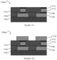
- FIGS. 17 A to 17 G are sectional views of a portion of an exemplary superconducting integrated circuit including stud vias and a superconducting metal polish stop layer, in accordance with the present systems and methods.
- FIGS. 18 A to 18 J are sectional views of a portion of a superconducting circuit including a kinetic inductor and a capacitor fabricated in separate layers, in accordance with the present systems and methods.
- the terms “carried by,” “carried on,” or variants thereof, and similarly the terms “over” and “above,” mean that one structure is directly or indirectly supported in at least some instances by another structure, for example directly on a surface thereof, spaced above or below a surface thereof by one or more intervening layers or structures or located therein.
- deposit Unless the specific context requires otherwise, throughout this specification the terms “deposit,” “deposited,” “deposition,” and the like are generally used to encompass any method of material deposition, including but not limited to physical vapor deposition (PVD), chemical vapor deposition (CVD), plasma-enhanced PVD, plasma-enhanced CVD, and atomic layer deposition (ALD).
- PVD physical vapor deposition
- CVD chemical vapor deposition
- ALD atomic layer deposition
- overlie or “overlies” are generally used to describe at least a portion of one layer at least partially in registration with at least a portion of another layer, either with or without one or more intermediary layers therebetween.
- FIG. 1 and FIGS. 2 A to 2 J An integrated process for fabricating a high kinetic inductance layer (also referred to in the present description as a kinetic inductor) and a capacitor is illustrated in FIG. 1 and FIGS. 2 A to 2 J .
- a high kinetic inductance layer is used for DAC (digital to analog converter) storage.
- Systems and methods related to DACs in superconducting integrated circuits are described in U.S. Pat. Nos. 8,098,179, 8,786,476, 7,876,248, 8,035,540, 8,604,944, and U.S.
- a capacitor is used for FMRR (frequency multiplexed resonant readout).
- FMRR frequency multiplexed resonant readout
- Systems and methods related to FMRR are described in International PCT patent application US2016/31885 “Frequency Multiplexed Resonator Input And/or Output For A Superconducting Device” which was filed 11 May 2016 and is incorporated herein by reference in its entirety.
- a superconducting integrated circuit can include a kinetic inductor and a capacitor.
- FIG. 1 is a flowchart illustrating a method 100 for fabricating a portion of a superconducting integrated circuit, according to one illustrated embodiment of the present disclosure.
- Method 100 includes acts 102 - 128 , though those of skill in the art will appreciate that in alternative embodiments certain acts may be omitted and/or additional acts may be added. Those of skill in the art will appreciate that the illustrated order of the acts is shown for exemplary purposes only and may change in alterative embodiments.
- Method 100 starts at 102 , for example in response to an initiation of the fabrication process.
- a first superconducting metal layer (WIRA) is deposited to overlie a substrate.
- the first superconducting metal layer is superconducting in a range of temperatures.
- the first superconducting metal layer includes niobium.
- WIRA is patterned by masking and etching at least a portion of WIRA to form a first wiring layer that includes one or more traces.
- a first dielectric (HILD) is deposited to overlie at least a portion of WIRA, and the dielectric is polished back to WIRA.
- the first dielectric is a high-loss dielectric such as silicon dioxide.
- polishing the first dielectric includes Chemical Mechanical Planarization (CMP).
- a second dielectric layer is deposited, and then patterned by masking and etching.
- the second dielectric layer is a thin layer of silicon dioxide intended to protect WIRA.
- a second layer of superconducting metal is deposited to overlie at least portions of WIRA and HILD.
- STV 1 includes aluminum.
- STV 1 includes niobium.
- STV 1 is patterned by masking and etching to form a first set of superconducting stud vias. The superconducting vias in the first set of superconducting vias are superconducting in a range of temperatures.
- a third dielectric (HILDSV 1 ) is deposited to overlie a) the layer of superconducting metal that forms the first set of superconducting vias, and b) the previously-deposited dielectric, and HILDSV 1 is polished back to the upper surface of at least some of the first set of superconducting stud via(s).
- HILDSV 1 is a high-loss dielectric.
- the polishing includes CMP.
- a high kinetic inductance layer is deposited, and patterned by masking and etching.
- the high kinetic inductance layer is also referred to as a flux storage layer.
- Kinetic inductance refers to the equivalent series inductance of mobile charge carriers in alternating electric fields, and is typically observed in high carrier mobility conductors such as superconductors.
- the high kinetic inductance layer can comprise a superconducting material selected for its high carrier mobility.
- the high kinetic inductance layer can be selected to provide an equivalent series inductance suitable for operation of circuit 200 j of FIG. 2 J , for example.
- the kinetic inductance of a superconducting wire is proportional to its length, and inversely proportional to its cross-sectional area, and inversely proportional to the density of Cooper pairs.
- the London penetration depth is an inherent property of a superconductor, and characterizes the distance to which a magnetic field penetrates into a superconductor.
- a superconductor having a larger London penetration depth has larger kinetic inductance for the same physical dimensions.
- high kinetic inductance layer 118 comprises a material that has a penetration depth at least three times the penetration depth of the superconducting metal forming first superconducting metal layer 104 , or second layer of superconducting metal 112 .
- the penetration depth is related to the density of Cooper pairs.
- Cooper pairs in a superconductor having a lower density of Cooper pairs travel faster and hence have greater kinetic energy, i.e., a larger proportion of energy is stored in the kinetic energy (kinetic inductance) than in the magnetic field (magnetic inductance) than for a superconductor with a higher density of Cooper pairs.
- the flux storage layer is a layer of titanium nitride (TiN). In other implementations, the flux storage layer is a layer of niobium nitride (NbN). In other implementations, the flux storage layer is a layer of one of niobium titanium nitride (NbTiN), molybdenum nitride (MoN), or tungsten silicide (WSi).
- a fourth dielectric layer is deposited and patterned by masking and etching. In some implementations, the fourth dielectric layer is a high-quality dielectric such as SiN.
- a third superconducting metal layer (WIRB) is deposited to overlie at least a portion of the fourth dielectric layer, and is patterned by masking and etching to form a second wiring layer that includes one or more traces.
- the second superconducting metal layer is superconducting in a range of temperatures.
- the second superconducting metal layer includes niobium.
- a fifth dielectric (HILD 3 ) is deposited to overlie at least a portion of WIRB, and is polished back to WIRB.
- HILD 3 is a high-loss dielectric such as silicon dioxide.
- polishing the fifth dielectric includes Chemical Mechanical Planarization (CMP).
- a second set of superconducting vias are formed, where at least some of the second set of superconducting vias provide a superconducting electrical coupling to WIRB.
- the second set of superconducting vias can be formed, for example by drilling holes in HILD 3 through to an upper surface of WIRB, and filling the holes with a fourth superconducting metal layer that is superconducting in a range of temperatures.
- the fourth superconducting metal layer includes niobium.
- FIGS. 2 A to 2 J show a sectional view of a portion of a superconducting circuit fabricated at successive stages of fabrication, according to method 100 of FIG. 1 .
- FIG. 2 A is a sectional view of a portion of a superconducting integrated circuit 200 a at a first stage of a fabrication process described by method 100 of FIG. 1 .
- Circuit 200 a comprises a substrate 202 and a first superconducting metal layer 204 (WIRA).
- substrate 202 is a silicon substrate.
- first superconducting metal layer 204 includes niobium.
- FIG. 2 B is a sectional view of a portion of a superconducting integrated circuit 200 b at a subsequent stage of the fabrication process.
- Superconducting integrated circuit 200 b can be formed from circuit 200 a of FIG. 2 A by patterning first superconducting metal layer 204 (WIRA) to form a first wiring layer that includes one or more traces, and by depositing a first dielectric layer 206 (HILD) and polishing first dielectric layer 206 back to the upper surface of first superconducting metal layer 204 .
- Patterning of first superconducting metal layer 204 can include masking and etching at least a portion of first superconducting metal layer 204 .
- Polishing first dielectric layer 206 can include CMP.
- An optional second layer of dielectric (not shown in FIGS. 2 A to 2 J ) can be deposited before depositing superconducting metal layer 208 .
- the second layer of dielectric for example, can be a thin layer of silicon dioxide intended to provide protection to the surface of WIRA.
- FIG. 2 C is a sectional view of a portion of a superconducting circuit 200 c at a subsequent stage of the fabrication process.
- Superconducting integrated circuit 200 c can be formed from circuit 200 b of FIG. 2 B by a) depositing a second superconducting metal layer 208 , b) patterning second superconducting metal layer 208 to form a first set of superconducting stud vias, c) depositing a third dielectric layer 210 (HILDSV 1 ), and d) polishing third dielectric layer 210 back to an upper surface of second superconducting metal layer 208 .
- second superconducting metal layer 208 includes aluminum.
- second superconducting metal layer 208 includes niobium. Patterning second superconducting metal layer 208 can include masking and etching at least a portion of second superconducting metal layer 208 . Polishing third dielectric layer 210 can include CMP.
- FIG. 2 D is a sectional view of a portion of a superconducting circuit 200 d at a subsequent stage of the fabrication process.
- Superconducting integrated circuit 200 d can be formed from circuit 200 c of FIG. 2 C by depositing a high kinetic inductance layer 212 to overlie second superconducting metal layer 208 and third dielectric layer 210 .
- High kinetic inductance layer 212 is also referred to in the present application as flux storage layer 212 .
- flux storage layer 212 includes TiN.
- FIG. 2 E is a sectional view of a portion of a superconducting circuit 200 e at a subsequent stage of the fabrication process.
- Superconducting integrated circuit 200 e can be formed from circuit 200 d of FIG. 2 D by patterning flux storage layer 212 .
- Patterning of flux storage layer 212 can include masking and etching at least a portion of flux storage layer 212 .
- a first portion of flux storage layer 212 can form an element of a kinetic inductor.
- a second portion of flux storage layer 212 can form an element of a capacitor.
- flux storage layer 212 can have a thickness of approximately 50 nm.
- patterning of flux storage layer 212 includes masking and etching at least a first portion of flux storage layer 212 to form an element of a kinetic inductor, and does not include masking and etching at least a second portion of flux storage layer 212 to form an element of a capacitor. Including at least a portion of flux storage layer 212 in a capacitor formed by the systems and methods of the present application is optional.
- FIG. 2 F is a sectional view of a portion of a superconducting circuit 200 f at a subsequent stage of the fabrication process.
- Superconducting integrated circuit 200 f can be formed from circuit 200 e of FIG. 2 E by depositing a fourth dielectric layer 214 to overlie at least a portion of flux storage layer 212 .
- fourth dielectric layer 214 is a high-quality dielectric such as SiN.
- FIG. 2 G is a sectional view of a portion of a superconducting circuit 200 f at a subsequent stage of the fabrication process.
- Superconducting integrated circuit 200 g can be formed from circuit 200 f of FIG. 2 F by patterning fourth dielectric layer 214 .
- Patterning of fourth dielectric layer 214 can include masking and etching at least a portion of fourth dielectric layer 214 .
- a first portion of fourth dielectric layer 214 can form a passivation insulating layer that can, for example, protect an element of a kinetic inductor.
- a second portion of fourth dielectric layer 214 can form a dielectric layer of a capacitor.
- fourth dielectric layer 214 can be a thin layer, for example fourth dielectric layer 214 can have a thickness of approximately 50 nm.
- FIG. 2 H is a sectional view of a portion of a superconducting circuit 200 f at a subsequent stage of the fabrication process.
- Superconducting integrated circuit 200 h can be formed from circuit 200 g of FIG. 2 G by depositing a third superconducting metal layer 216 , and patterning third superconducting metal layer 216 to form a second wiring layer that includes one or more traces.
- Patterning third superconducting metal layer 216 can include masking and etching at least a portion of third superconducting metal layer 216 .
- third superconducting metal layer 216 includes niobium.
- FIG. 2 I is a sectional view of a portion of a superconducting circuit 200 i at a subsequent stage of the fabrication process.
- Superconducting integrated circuit 200 i can be formed from circuit 200 h of FIG. 2 H by depositing a fifth dielectric layer 218 (HILD 3 ), and forming one or more holes 220 (such as holes 220 - 1 and 220 - 2 called out in FIG. 2 I ) in fifth dielectric layer 218 to an upper surface of second wiring layer 216 .
- holes 220 can be formed by drilling holes in fifth dielectric layer 218 .
- FIG. 2 J is a sectional view of a portion of a superconducting circuit 200 j at a subsequent stage of the fabrication process.
- Superconducting integrated circuit 200 j can be formed from circuit 200 i of FIG. 2 I by depositing a fourth superconducting metal layer 222 in holes 220 to form superconducting vias to third superconducting metal layer 216 .
- fourth superconducting metal layer 222 includes niobium.
- superconducting vias to the third superconducting metal layer 216 are formed using a fabrication method similar to the method described in reference to FIG. 2 C .
- an optional fifth layer of dielectric such as a thin layer of silicon dioxide (not shown in FIGS. 2 A to 2 J ) can be deposited to provide protection to the surface of third superconducting metal layer 216 .
- a fourth superconducting metal layer 222 is deposited, and patterned to form a second set of superconducting stud vias.
- a sixth dielectric layer 218 is deposited, and polished back to an upper surface of fourth superconducting metal layer 222 .
- Superconducting integrated circuit 200 j includes a via wall 224 , a kinetic inductor 226 , and a capacitor 228 .
- Kinetic inductor 226 comprises two electrodes 230 and 232 , each electrode electrically coupled to a trace formed in superconducting metal layer 204 .
- Capacitor 228 comprises two electrodes 234 and 236 .
- Electrode 234 is electrically coupled to a trace formed in first superconducting metal layer 204 .
- Electrode 236 is electrically coupled to a trace formed in fourth superconducting metal layer 222 .
- capacitor 228 includes at least of portion of flux storage layer 212 and at least a portion of fourth dielectric layer 214 .
- capacitor 228 includes at least a portion of fourth dielectric layer 214 , and does not include at least a portion of flux storage layer 212 .
- An advantage of the systems and methods described above with reference to FIG. 1 and FIGS. 2 A to 2 J is that the number of processing acts in the fabrication of a superconducting integrated circuit that includes a kinetic inductor and a capacitor can be reduced. Fewer processing acts typically results in lower fabrication costs and higher fabrication yields.
- the high kinetic inductance layer in a kinetic inductor and the high kinetic inductance layer in a capacitor in the same superconducting integrated circuit are formed by separate acts, for example by using separate mask and etch acts for the kinetic inductor and the capacitor.
- act 118 of FIG. 1 can include separate mask and etch for a kinetic inductor and a capacitor in the same superconducting integrated circuit.
- the kinetic inductor and the capacitor are formed in separate layers of a superconducting integrated circuit.
- a process for fabricating a superconducting integrated circuit including a kinetic inductor and a capacitor that are each in separate layers is illustrated in FIG. 18 A to 18 J .
- the stud via is a superconducting stud via in a superconducting integrated circuit.
- a feature of the systems and methods described below is that a hard mask (e.g. silicon dioxide) and a soft mask (e.g. photoresist) can be used in combination as a dual mask.
- An advantage of the dual mask approach is that it avoids, or at least reduces, complications caused by step height in the lithography process.
- Another advantage is that the lower layer (which encloses the stud via) can be reduced in size, for example to 100 nm.
- the stud via pattern and the wiring layer pattern can be defined first, and then the patterns transferred using a process that exploits differential selectivity between the hard mask material and the soft mask material.
- An example process is reactive ion etching.
- FIG. 3 is a flowchart illustrating a method 300 for fabricating a portion of a superconducting integrated circuit, according to one illustrated embodiment of the present disclosure.
- Method 300 includes acts 302 - 320 , though those of skill in the art will appreciate that in alternative embodiments certain acts may be omitted and/or additional acts may be added. Those of skill in the art will appreciate that the illustrated order of the acts is shown for exemplary purposes only and may change in alterative embodiments.
- Method 300 starts at 302 , for example in response to an initiation of the fabrication process.
- a first superconducting metal layer (WIRB) is deposited to overlie a substrate.
- the first superconducting metal layer is superconducting in a range of temperatures.
- the first superconducting metal layer comprises niobium.
- the first superconducting metal layer can be a wiring layer.
- the wiring layer can be patterned to form one or more superconducting traces.
- an etch stop layer is deposited to overlie at least a portion of the first superconducting metal layer WIRB.
- the etch stop layer is superconducting in a range of temperatures.
- the etch stop layer is a thin layer of aluminum.
- a second superconducting metal layer is deposited to overlie at least a portion of the etch stop layer.
- the second superconducting metal layer is superconducting in a range of temperatures.
- the second superconducting metal layer comprises at least one of niobium and aluminum.
- the second superconducting metal layer is a stud via layer.
- a hard mask is deposited, or transferred, to overlie a portion of the stud via layer.
- the hard mask comprises silicon dioxide.
- a hard mask is a material used in fabrication of an integrated circuit (e.g., a superconducting integrated circuit) as an etch mask in place of a polymer or other organic soft mask (or photoresist) material. The material of the hard mask is less vulnerable than a soft mask to etching by reactive gases such as oxygen, fluorine, or chlorine.
- a soft mask is deposited to overlie at least a portion of the hard mask and at least a portion of the stud via layer.
- the soft mask comprises photoresist.
- a soft mask is a material used in fabrication of an integrated circuit (e.g., a superconducting integrated circuit), and is typically a polymer or other organic soft resist material. The soft mask is more easily etched than the hard mask by reactive gases during plasma etching, for example.
- the exposed stud via layer and the underlying or exposed etch stop layer are etched.
- the soft mask is stripped, and optionally rinsed.
- the exposed stud via layer, wiring layer and etch stop layer are etched.
- method 300 ends.
- the soft mask is a photoresist and a cleaning agent can be used to rinse off the photoresist after it is stripped at 316 .
- common cleaning agents such as isopropanol can corrode the wiring layer. It can be advantageous to use a non-corrosive cleaning agent, for example, EKC4000TM which is commercially available from DuPont, to rinse off the photoresist.
- FIGS. 4 A to 4 F are sectional views of a portion of an exemplary superconducting integrated circuit which includes a stud via, at various stages of its fabrication, in accordance with the present systems and methods.
- FIG. 4 A is a sectional view of a portion of a superconducting integrated circuit 400 a at a first stage of a fabrication process described by method 300 of FIG. 3 .
- Circuit 400 a comprises a first superconducting metal layer 402 and an etch stop layer 404 .
- first superconducting metal layer 402 overlies a substrate.
- First superconducting metal layer 402 is superconducting in a range of temperatures.
- first superconducting metal layer 402 comprises niobium.
- the first superconducting metal layer can be a wiring layer.
- the wiring layer can be patterned to form one or more superconducting traces.
- Etch stop layer 404 is superconducting in a range of temperatures. In some implementations, etch stop layer 404 is a thin layer of aluminum.
- FIG. 4 B is a sectional view of a portion of a superconducting integrated circuit 400 b at a subsequent stage of the fabrication process.
- Superconducting integrated circuit 400 b can be formed from circuit 400 a of FIG. 4 A by depositing a second superconducting metal layer 406 to overlie at least a portion of etch stop layer 404 .
- Second superconducting metal layer 406 is superconducting in a range of temperatures.
- second superconducting metal layer 406 comprises at least one of niobium and aluminum.
- Second superconducting metal layer can be a stud via layer.
- FIG. 4 C is a sectional view of a portion of a superconducting circuit 400 c at a subsequent stage of the fabrication process.
- Superconducting integrated circuit 400 c can be formed from circuit 400 b of FIG. 4 B by depositing, or transferring, a hard mask 408 .
- hard mask 408 comprises silicon dioxide.
- FIG. 4 D is a sectional view of a portion of a superconducting circuit 400 d at a subsequent stage of the fabrication process.
- Superconducting integrated circuit 400 d can be formed from circuit 400 c of FIG. 4 C by depositing, or transferring, a soft mask 410 to overlie at least a portion of the hard mask and at least a portion of the stud via layer.
- the soft mask comprises photoresist.
- FIG. 4 E is a sectional view of a portion of a superconducting circuit 400 e at a subsequent stage of the fabrication process.
- Superconducting integrated circuit 400 e can be formed from circuit 400 d of FIG. 4 D by etching second superconducting metal layer 406 (the stud via layer) to etch stop layer 404 .
- FIG. 4 F is a sectional view of a portion of a superconducting circuit 400 f at a subsequent stage of the fabrication process.
- Superconducting integrated circuit 400 f can be formed from circuit 400 e of FIG. 4 E by etching second superconducting layer 406 , etch stop layer 404 , and first superconducting layer 402 to form a superconducting stud via 412 .
- Superconducting stud via 412 can include at least a portion of each of second superconducting layer 406 , etch stop layer 404 , and first superconducting layer 402 .
- the portion of first superconducting metal layer 402 that forms part of superconducting stud via 412 is portion 414 .
- FIGS. 5 A to 5 C are plan views of a portion of an example superconducting circuit at a various stages of a self-aligned dual-mask process, in accordance with the present systems and methods.
- the self-aligned dual-mask process illustrated in FIGS. 5 A to 5 C can be elements of a fabrication process to form superconducting stud vias, such as the fabrication process described above with reference to FIGS. 3 and 4 A to 4 F .
- FIG. 5 A is a plan view of a portion of an example superconducting integrated circuit 500 a comprising a hard mask 502 .
- Hard mask 502 can be patterned by a first etch process.
- Hard mask 502 can define a stud via, for example.
- FIG. 5 B is a plan view of a portion of an example superconducting integrated circuit 500 b comprising hard mask 502 and soft mask 504 .
- Soft mask 504 can be deposited, or transferred, to overlie at least a portion of hard mask 502 .
- Soft mask 504 can define a wire, for example.
- FIG. 5 C is a plan view of a portion of an example superconducting integrated circuit 500 c comprising hard mask 502 and soft mask 504 , after hard mask 502 has been etched a second time.
- a stud via and wire defined by hard mask 502 and soft mask 504 , respectively, can be self-aligned.
- FIG. 5 D is a plan view of a portion of an example superconducting integrated circuit 500 d showing enclosure of a stud via 506 (defined by etched hard mask 502 of FIGS. 5 A to 5 C , for example) by an upper wiring layer 508 .
- Stud via 506 can provide a superconducting electrical coupling between upper wiring layer 508 and a lower wiring layer 510 .
- An advantage of the configuration illustrated in FIG. 5 D is that the etch of upper wiring layer 508 is less likely to affect stud via 506 , which may create planarization problems at a later stage in the fabrication process.
- the enclosure is 100 nm.
- FIG. 5 E is a plan view of a portion of an example superconducting integrated circuit 500 e showing a stud via 512 providing electrical coupling between two wires 514 and 516 that cross each other.
- the cross-coupling shown in FIG. 5 E can be formed by adding an etch stop layer under the wiring layer of upper wire 514 .
- the etch stop layer can be, for example, a thin layer of aluminum.
- the etch stop layer can be etched away after the upper wiring layer etch.
- FIG. 6 is a flowchart illustrating a method 600 for fabricating a portion of a superconducting integrated circuit including stud vias, in accordance with the present systems and methods.
- Method 600 includes acts 602 - 622 , though those of skill in the art will appreciate that in alternative embodiments certain acts may be omitted and/or additional acts may be added. Those of skill in the art will appreciate that the illustrated order of the acts is shown for exemplary purposes only and may change in alterative embodiments.
- Method 600 starts at 602 , for example in response to an initiation of the fabrication process.
- a first superconducting metal layer is deposited to overlie a substrate.
- the first superconducting metal layer is superconducting in a range of temperatures.
- the first superconducting metal layer comprises niobium.
- the first superconducting metal layer can be a wiring layer.
- the wiring layer can be patterned to form one or more superconducting traces.
- the first superconducting metal layer is masked and etched to form the wiring layer.
- a first dielectric layer is deposited to overlie at least a portion of the first superconducting metal layer, and polished back to an upper surface of the first superconducting metal layer.
- the first dielectric comprises silicon dioxide.
- a second dielectric layer is deposited to overlie at least a portion of the first superconducting metal layer, and then masked and etched.
- the second dielectric layer is a thin layer of silicon dioxide.
- a second superconducting metal layer is deposited to overlie at least a portion of the wiring layer.
- the second superconducting metal layer is superconducting in a range of temperatures.
- the second superconducting metal layer comprises at least one of niobium and aluminum.
- the second superconducting metal layer is a stud via layer.
- the second superconducting metal is masked and etched to form one or more stud vias.
- a third dielectric layer is deposited, and polished back to an upper surface of at least one of the stud vias. In some implementations, polishing includes CMP. If, at 618 , the fabrication of stud vias is complete because no more stud via layers are desired to be added, control of method 600 proceeds to 620 and method 600 ends.
- control of method 600 proceeds to 622 , and a fourth dielectric layer is deposited, masked and etched. Acts 604 to 618 are repeated to add another stud via layer. In one implementation, method 600 does not include act 622 and act 618 proceeds directly to act 604 .
- some oxide can remain on the upper surface of a stud via.
- acts can be included to at least reduce the amount of oxide remaining on the upper surface of the via.
- One approach is to use another mask and perform a gentle etch of the upper surface of the stud via to remove at least some of the oxide remaining after 618 .
- Another approach is to use a reverse mask process, and replace 618 by the following: i) depositing a third dielectric layer of at least approximately the same thickness as the stud via layer, ii) masking, and then etching dielectric from at least a portion of the third dielectric layer that overlies the stud via, and iii) performing a gentle CMP (buffer) to remove at least some of the remaining dielectric that overlies the stud via after etching.
- a reverse mask process depositing a third dielectric layer of at least approximately the same thickness as the stud via layer, ii) masking, and then etching dielectric from at least a portion of the third dielectric layer that overlies the stud via, and iii) performing a gentle CMP (buffer) to remove at least some of the remaining dielectric that overlies the stud via after etching.
- FIGS. 7 A to 7 G are sectional views of a portion of an exemplary superconducting integrated circuit including stud vias, at various stages of their fabrication, in accordance with the present systems and methods.
- FIG. 7 A is a sectional view of a portion of a superconducting integrated circuit 700 a at a first stage of a fabrication process described by method 600 of FIG. 6 .
- Circuit 700 a comprises a substrate 702 and a first wiring layer 704 deposited and patterned to overlie at least a portion of substrate 702 .
- First wiring layer 704 is superconducting in a range of temperatures.
- first wiring layer 704 comprises niobium.
- first wiring layer 704 comprises aluminum.
- the wiring layer comprises one or more superconducting traces.
- FIG. 7 B is a sectional view of a portion of a superconducting integrated circuit 700 b at a subsequent stage of the fabrication process.
- Superconducting integrated circuit 700 b can be formed from circuit 700 a of FIG. 7 A by depositing a first dielectric layer 706 to overlie at least a portion of substrate 702 and first wiring layer 704 , and polishing first dielectric layer 706 back to an upper surface of at least a portion of first wiring layer 704 .
- first dielectric layer 706 comprises silicon dioxide.
- polishing first dielectric layer 706 includes CMP.
- FIG. 7 C is a sectional view of a portion of a superconducting circuit 700 c at a subsequent stage of the fabrication process.
- Superconducting integrated circuit 700 c can be formed from circuit 700 b of FIG. 7 B by depositing, then masking and etching, a second dielectric layer 708 to overlie at least a portion of first dielectric layer 706 .
- second dielectric layer 708 is a thin layer of silicon dioxide.
- FIG. 7 D is a sectional view of a portion of a superconducting circuit 700 d at a subsequent stage of the fabrication process.
- Superconducting integrated circuit 700 d can be formed from circuit 700 c of FIG. 7 C by depositing a second superconducting metal layer 710 to overlie at least a portion of first wiring layer 704 and second dielectric layer 708 .
- Second superconducting metal layer 710 is superconducting in a range of temperatures.
- second superconducting metal layer 710 comprises at least one of niobium and aluminum.
- second superconducting metal layer 710 comprises aluminum with a thin niobium layer that overlies at least a portion of second superconducting metal layer 710 .
- the thin niobium layer can function as a polish stop or protective layer.
- Second superconducting metal layer can be a stud via layer.
- FIG. 7 E is a sectional view of a portion of a superconducting circuit 700 e at a subsequent stage of the fabrication process.
- Superconducting integrated circuit 700 e can be formed from circuit 700 d of FIG. 7 D by masking and etching second superconducting metal layer 710 of FIG. 7 D to form one or more superconducting stud vias, for example 710 a and 710 b of FIG. 7 E .
- FIG. 7 F is a sectional view of a portion of a superconducting circuit 700 f at a subsequent stage of the fabrication process.
- Superconducting integrated circuit 700 f can be formed from circuit 700 e of FIG. 7 E by depositing a third dielectric layer 712 , and polishing third dielectric layer 712 back to an upper surface of at least a portion of stud vias 710 a and 710 b .
- third dielectric layer 712 comprises silicon dioxide.
- polishing third dielectric layer 712 includes CMP.
- FIG. 7 G is a sectional view of a portion of a superconducting circuit 700 g at a subsequent stage of the fabrication process.
- Superconducting integrated circuit 700 g can be formed from circuit 700 f of FIG. 7 F by adding the following:
- second wiring layer 716 comprises niobium.
- second stud via layer 722 comprises at least one of niobium and aluminum.
- fifth dielectric layer 718 and seventh dielectric layer 724 comprise silicon dioxide.
- sixth dielectric layer 720 is a thin layer of silicon dioxide. In some implementations, the thickness of sixth dielectric layer 720 is in the range 50 nm to 200 nm.
- FIG. 7 G is a sectional view of a portion of a superconducting circuit 700 h at a subsequent stage of a fabrication process wherein:
- FIG. 7 H illustrates one example implementation wherein second dielectric layer 708 , fourth dielectric layer 714 , and sixth dielectric layer 720 are omitted from superconducting integrated circuit 700 g of FIG. 7 G .
- second dielectric layer 708 , fourth dielectric layer 714 , and sixth dielectric layer 720 can be omitted.
- FIGS. 17 A to 17 G A process for fabricating a superconducting integrated circuit including stud via formation with a polish stop layer is illustrated in FIGS. 17 A to 17 G .
- the systems and methods described below may measure interlayer misalignment on superconducting integrated circuits to an accuracy of, for example, 10 nm.
- Optical measurements of interlayer misalignment can have shortcomings.
- the systems and methods described below use an electrical measurement for determining layer misalignment.
- Electrical verniers can detect layer misalignment by measuring resistance during wafer-probing with a four-wire measurement.
- the four-wire measurement is illustrated in FIG. 8 C and described in more detail below.
- FIG. 8 A is a sectional view of a portion of an exemplary superconducting integrated circuit which includes an electrical vernier 800 , in accordance with the present systems and methods.
- Vernier 800 comprises a first mark 802 in a first wiring layer (e.g. WIRA), a second mark 804 in a second wiring layer (e.g. WIRB), and a stud via 806 .
- Mark 804 overlaps stud via 806 at resistive overlap region 808 .
- Appropriate selection of the dimensions of marks 802 and 804 , and stud via 806 can cause resistive overlap region 808 to dominate a resistance measurement from the first wiring layer to the second wiring layer through the stud via.
- marks 802 and 804 , and stud via 806 can be selected to be large enough that they have a much lower resistance than resistive overlap region 808 .
- FIG. 8 B is a plan view of a portion of the exemplary superconducting integrated circuit of FIG. 8 A which includes electrical vernier 800 .
- First mark 802 has width W 1 , length (L 1 +L 3 ), and thickness t wire (not shown in FIG. 8 B ).
- Second mark 804 has width W 2 , length (L 2 +d), and thickness t wire .
- Stud via 806 has width W 3 and length L 3 . Mark 804 is offset laterally from mark 802 by distance ⁇ .
- first mark 802 can be offset with respect to stud via 806 parallel to the length of first mark 802 and/or perpendicular to the length of first mark 802 .
- FIG. 8 C is a schematic showing a portion of the exemplary superconducting integrated circuit which includes electrical vernier 800 of FIG. 8 A with leads attached for a four-wire measurement.
- the circuit includes four leads 810 a , 810 b , 810 c , and 810 d .
- Two leads 810 a and 810 b are electrically connected to mark 802
- two leads 810 c and 810 d are electrically connected to mark 804 .
- FIG. 8 C illustrates a configuration that can perform an interlayer misalignment measurement using electrical vernier 800 .
- the total resistance fora vernier mark is the sum of contributions from the upper and lower wires, and the overlaps between the stud via and the upper and lower wires.
- a suitable selection of wire and stud via dimensions can cause the resistance of the overlap between the stud via and the upper wire to dominate the measured value of total resistance. Suitable values can be found, for example, by sweeping through possible geometries and, for each one, determining the change in resistance between typical misalignments. Values can be selected, for example, based on achieving a desired change in resistance for a given misalignment while maintaining a small footprint on the chip.
- the change in resistance is determined between offsets of 0 nm and 20 nm. In one measurement scenario, a change in resistance of between 0.5% and 5% is suitable for measuring interlayer misalignment.
- R total ⁇ N ⁇ b ⁇ ( L A t w ⁇ i ⁇ r ⁇ e ⁇ W A + ( t w ⁇ i ⁇ r ⁇ e + t v ⁇ i ⁇ a ) L V ⁇ W V + t w ⁇ i ⁇ r ⁇ e d ⁇ ( W B - ⁇ ) + L B t w ⁇ i ⁇ r ⁇ e ⁇ W B )
- FIG. 9 is an example plot illustrating a variation of resistance (in ohms) as a function of a lateral offset E (in nm) of an edge of a top wiring layer from an edge of a stud via in the exemplary superconducting integrated circuit of FIGS. 8 A to 8 C , in accordance with the present systems and methods.
- Each point on the graph of FIG. 9 is a measurement of resistance for a different vernier mark.
- the misalignment can be inferred from the position along the horizontal axis of the knee of the curve in FIG. 9 .
- the example shown in FIG. 9 is for an interlayer misalignment of 32 nm.
- the knee of the curve occurs at 32 nm on the horizontal axis.
- overetch of the stud via layer can occur when etching the wire layer above it.
- the overetch is in the range 120 nm to 200 nm.
- the interlayer misalignment can be measured in the presence of overetch using an electrical vernier such as vernier 800 of FIG. 8 A .
- there can be an overetch of the stud via layer when etching the upper wire layer e.g. overetch of STVB when etching WIRB.
- there can be a complete overetch of the stud via layer in which case the stud via no longer extends beyond the boundaries of the upper wire layer.
- An advantage of a complete overetch is that the measured misalignment between layers is a direct measurement of the misalignment between the upper and lower layers.
- the selection of dimensions for the vernier marks can be generalized to an overetch between no overetch and complete overetch as follows:
- the stud via layer can be misaligned in fabrication relative to the lower wiring layer (WIRA) by up to 100 nm in the along-wire dimension and the across-wire dimension (e.g., either case denominated as “within plane” misalignment).
- the upper wiring layer (WIRB) can be misaligned in fabrication relative to WIRA by up to 100 nm in the along-wire dimension and the across-wire dimension (e.g., either case either case denominated as “within plane” misalignment).
- STVB is larger than the overlap of WIRA and WIRB by at least 100 nm in the along-wire direction, and STVB is larger than the overlap of WIRA and WIRB by at least 225 nm in the across-wire direction.
- the distance between edges of the STVB is at least 1,000 nm.
- the overlap of WIRA and WIRB is 250 nm ⁇ 250 nm.
- FIGS. 15 A and 15 B are views of an exemplary superconducting integrated circuit 1500 which includes overetch of a stud via layer.
- FIGS. 15 A and 15 B label the dimensions of circuit 1500 , including upper and lower wires, and a stud via.
- FIG. 15 A is a plan view and FIG. 15 B is a sectional view.
- Example dimensions for one implementation are listed in Table 1 below.
- some electrical verniers are constructed using offsets of WIRA with respect to STVB, and other electrical verniers are constructed using offsets of WIRB with respect to STVB. These verniers can be used to separate the combined effects of interlayer misalignment between WIRA and STVB, and WIRB and STVB.
- One approach to measuring interlayer misalignment is to use a chain of electrical verniers. This approach can overcome some of the challenges of measuring low resistances.
- One challenge is the heating that can be caused by currents flowing in the wires. For example, a current of more than 1 mA through 250 nm wires can cause sufficient heating to distort the resistance measurement.
- a better approach for mitigating heating caused by current flow, and one that can be applied to most measurement instruments, is to increase the resistance of the electrical verniers, for example by constructing a chain of electrical verniers.
- a chain of up to, for example, 1,000 electrical verniers can be used to measure interlayer misalignment.
- the dimensions of the electrical verniers can be selected to provide a desired measurement sensitivity.
- FIG. 10 A is a plan view of a portion of an exemplary superconducting integrated circuit which includes an electrical vernier 1000 a , in accordance with the present systems and methods.
- Vernier 1000 a comprises a first mark 1002 , a second mark 1004 , and a stud via 1006 .
- FIG. 10 B is a plan view of a portion of an exemplary superconducting integrated circuit which includes an example implementation of a chain of electrical verniers 1000 b , in accordance with the present systems and methods.
- Chain 1000 b comprises four electrically connected electrical verniers 1008 , 1010 , 1012 , and 1014 .
- FIG. 10 C is a plan view of a portion of an exemplary superconducting integrated circuit which includes another example implementation of a chain of electrical verniers 1000 c , in accordance with the present systems and methods.
- Chain 1000 c comprises four electrically connected electrical verniers 1016 , 1018 , 1020 , and 1022 .
- Chain 1000 c is a mirror image of chain 1000 b in the vertical direction.
- Chains 1000 b and 1000 c are example implementations having different configurations of electrical verniers.
- chains 1000 b and 1000 c each comprise four verniers, other implementations can include a suitable number of verniers.
- a chain can include, for example, 1,000 verniers.
- the total resistance of the chain of verniers can be selected by adjusting the chain length.
- the resistance can be selected to be in a suitable range for the wafer-probing system. In one example implementation, a resistance of 2,500 ohm can be selected. With a probe able to measure resistances to within 0.2%, interlayer misalignments as small as 2 nm can be detected. In another example implementation, resistance is measured for a chain of 3,200 verniers, the total resistance being approximately 6,000 ohm.
- FIG. 11 is a schematic of an example implementation of a Wheatstone bridge 1100 , showing an arrangement of four resistors.
- two arms of the bridge consist of chains in the orientation shown in FIG. 10 B , each providing a respective resistance of R 1 .
- the opposite two arms of the bridge consist of the same chains mirrored in the vertical direction as shown in FIG. 10 C , each providing a respective resistance of R 2 .
- R 1 and R 2 are equal, and a zero voltage is measured across the bridge.
- the overlap area on R 1 is the same, and the resistance is unchanged.
- the overlap area is smaller as a result of the misalignment of the upper and the lower layers. Consequently, resistance R 2 is higher than when the layers are aligned, resulting in a non-zero voltage across the bridge.
- a misalignment in the opposite direction causes R 1 to increase in resistance, and R 2 to stay the same resistance. The resulting non-zero voltage across the bridge can have an opposite sign to the first instance.
- FIG. 12 is an example plot illustrating a variation of measured voltage (in mV) as a function of misalignment (in nm), in accordance with the present systems and methods.
- a measured voltage can be used to determine an interlayer misalignment.
- Values of the bridge can be selected to provide a suitable sensitivity to interlayer misalignment.
- the measured voltage is zero if there is no interlayer misalignment.
- a positive misalignment can cause a negative measured voltage.
- a measured voltage of ⁇ 20 mV can result from an interlayer misalignment of approximately 100 nm.
- bridge 1100 of FIG. 11 can measure sub-nm interlayer misalignments.
- On-chip transmission lines are ideally designed to be fully enclosed (except at the point of coupling) and 50 ohm matched. Impedance matching ensures that minimal, or at least reduced, signal distortion occurs. Enclosing the transmission line ensures minimal, or at least reduced, coupling to box modes or on-chip structures. Additionally, the shield enclosing the transmission line can at least partially isolate an on-chip device (for example, a qubit) from high-frequency noise propagating on the line.
- an on-chip device for example, a qubit
- the systems and methods described below with reference to FIGS. 13 A and 13 B include a transmission line with a center conductor having a large kinetic inductance.
- the center conductor of the transmission line can include titanium nitride (TiN).
- TiN titanium nitride
- a higher inductance of the center line can compensate for a higher capacitance between the center line and ground.
- This approach can be used to form a fully-enclosed, 50 ohm transmission line in as few as three metal layers in the fabrication stack.
- FIGS. 13 A and 13 B show two illustrative embodiments of the approach.
- FIG. 13 A is a sectional view of a portion of an exemplary superconducting integrated circuit 1300 a which includes an on-chip transmission line, in accordance with the present systems and methods.
- Circuit 1300 a comprises a substrate 1302 and a first superconducting metal layer 1304 deposited to overlie at least a portion of substrate 1302 .
- substrate 1302 includes silicon.
- First superconducting metal layer 1304 is superconducting in a range of temperatures.
- first superconducting metal layer 1304 includes niobium.
- first superconducting metal layer 1304 has a thickness of 300 nm.
- first superconducting metal layer 1304 is a wiring layer.
- First superconducting metal layer 1304 can be patterned to form a first set of one or more superconducting traces.
- Circuit 1300 a further comprises a first dielectric layer 1306 overlying at least a portion of first superconducting metal layer 1304 , and a high kinetic inductance layer 1308 overlying at least a portion of first dielectric layer 1306 .
- circuit 1300 a further comprises a passivation layer 1310 overlying at least a portion of high kinetic inductance layer 1308 and first dielectric layer 1306 .
- Passivation layer 1310 may be a diffusion barrier to at least reduce oxygen diffusion into high kinetic inductance layer 1308 , the diffusion resulting, for example, from the use of oxygen plasma to strip photoresist. In other implementations, passivation layer 1310 is omitted from the fabrication stack.
- kinetic inductance refers to the equivalent series inductance of mobile charge carriers in alternating electric fields, and is typically observed in high carrier mobility conductors such as superconductors.
- High kinetic inductance layer 1308 can comprise a superconducting material selected for its high carrier mobility.
- High kinetic inductance layer 1308 can be selected to provide an equivalent series inductance suitable for operation of circuit 1300 a .
- the kinetic inductance of a superconducting wire is proportional to its length, and inversely proportional to its cross-sectional area, and inversely proportional to the density of Cooper pairs.
- the London penetration depth is an inherent property of a superconductor, and characterizes the distance to which a magnetic field penetrates into a superconductor.
- a superconductor having a larger London penetration depth has larger kinetic inductance for the same physical dimensions.
- high kinetic inductance layer 1308 comprises a material that has a penetration depth at least three times the penetration depth of the superconducting metal forming first superconducting metal layer 1304 .
- the penetration depth is related to the density of Cooper pairs.
- Cooper pairs in a superconductor having a lower density of Cooper pairs travel faster and hence have greater kinetic energy, i.e., a larger proportion of energy is stored in the kinetic energy (kinetic inductance) than in the magnetic field (magnetic inductance) than for a superconductor with a higher density of Cooper pairs.
- the kinetic inductor has length 1,000 nm, width 1,000 nm, and thickness 50 nm.
- the kinetic inductance is approximately 5 pH.
- the inductance of a similarly dimensioned lower kinetic inductance wire would be approximately 0.5 pH.
- the high kinetic inductance layer 1308 can be patterned to form a first set of one or more high kinetic inductance structures or traces.
- first dielectric layer 1306 includes silicon dioxide.
- first dielectric layer 1306 has a thickness of 200 nm.
- High kinetic inductance layer 1308 is superconducting in a range of temperatures.
- high kinetic inductance layer 1308 includes titanium nitride (TiN).
- high kinetic inductance layer 1308 includes niobium nitride (NbN).
- high kinetic inductance layer 1308 includes at least one of TiN, NbN, niobium titanium nitride (NbTiN), molybdenum nitride (MoN), and tungsten silicide (WSi).
- high kinetic inductance layer 1308 has a thickness of 50 nm.
- passivation layer 1310 includes silicon nitride (SiN). In some implementations, passivation layer 1310 has a thickness of 50 nm.
- Circuit 1300 a further comprises a second superconducting metal layer 1312 deposited to overlie at least a portion of high kinetic inductance layer 1308 (and optional passivation layer 1310 ).
- Second superconducting metal layer 1312 is superconducting in a range of temperatures.
- second superconducting metal layer 1312 includes niobium.
- second superconducting metal layer 1312 has a thickness of 300 nm.
- second superconducting metal layer 1312 is a wiring layer.
- Second superconducting metal layer 1312 can be patterned to form a second set of one or more superconducting traces.
- Circuit 1300 a further comprises a second dielectric layer 1314 overlying second superconducting metal layer 1312 .
- second dielectric layer 1314 includes silicon dioxide.
- second dielectric layer 1314 has a thickness of 200 nm.
- Circuit 1300 a further comprises a third superconducting metal layer 1316 deposited to overlie at least a portion of second dielectric layer 1314 .
- Third superconducting metal layer 1316 is superconducting in a range of temperatures.
- third superconducting metal layer 1316 includes niobium.
- third superconducting metal layer 1316 has a thickness of 300 nm.
- third superconducting metal layer 1316 is a wiring layer.
- Third superconducting metal layer 1316 can be patterned to form a third set of one or more superconducting traces.
- each of the layers in circuit 1300 a can be selected in combination with a center line width to achieve a desired 50 ohm impedance.
- FIG. 13 B is a sectional view of a portion of another exemplary superconducting integrated circuit 1300 b which includes an on-chip transmission line, in accordance with the present systems and methods.
- Circuit 1300 b comprises a substrate 1302 and a first superconducting metal layer 1304 deposited to overlie at least a portion of substrate 1302 .
- substrate 1302 includes silicon.
- First superconducting metal layer 1304 is superconducting in a range of temperatures.
- first superconducting metal layer 1304 includes niobium.
- first superconducting metal layer 1304 has a thickness of 300 nm.
- first superconducting metal layer 1304 is a wiring layer.
- First superconducting metal layer 1304 can be patterned to form a first set of one or more superconducting traces.
- Circuit 1300 b further comprises a first dielectric layer 1306 overlying at least a portion of first superconducting metal layer 1304 , and a high kinetic inductance layer 1308 overlying at least a portion of first dielectric layer 1306 .
- circuit 1300 b further comprises a passivation layer 1310 overlying at least a portion of high kinetic inductance layer 1308 and first dielectric layer 1306 .
- passivation layer 1310 is omitted from the fabrication stack.
- first dielectric layer 1306 includes silicon dioxide. In some implementations, first dielectric layer 1306 has a thickness of 200 nm.
- High kinetic inductance layer 1308 is superconducting in a range of temperatures. In some implementations, high kinetic inductance layer 1308 includes titanium nitride (TiN). In some implementations, high kinetic inductance layer 1308 has a thickness of 50 nm.
- passivation layer 1310 includes silicon nitride (SiN). In some implementations, passivation layer 1310 has a thickness of 50 nm.
- Circuit 1300 b further comprises a second dielectric layer 1318 overlying passivation layer 1310 .
- second dielectric layer 1318 includes silicon dioxide.
- second dielectric layer 1318 has a thickness of 200 nm.
- Circuit 1300 b further comprises a second superconducting metal layer 1320 deposited to overlie at least a portion of second dielectric layer 1318 .
- Second superconducting metal layer 1320 is superconducting in a range of temperatures.
- second superconducting metal layer 1320 includes niobium.
- first superconducting metal layer 1320 has a thickness of 300 nm.
- second superconducting metal layer 1320 is a wiring layer.
- Second superconducting metal layer 1320 can be patterned to form a second set of one or more superconducting traces.
- each of the layers in circuit 1300 b can be selected in combination with a center line width to achieve a desired 50 ohm impedance.
- Two ground planes can be formed by the lowermost and uppermost wiring layers in FIGS. 13 A and 13 B .
- the two ground planes can be connected by vias.
- the two ground planes can be connected by superconducting stud vias.
- a continuous via wall is used to connect the two ground planes.
- the vias can be separated from the center line on each side by three times the width of the centerline. An advantage of providing this separation is that the impact of the stud vias on the impedance can be eliminated, or at least reduced.
- FIG. 13 C is a sectional view of a portion of an exemplary superconducting integrated circuit 1300 c which includes an on-chip transmission line and connected ground planes, in accordance with the present systems and methods.
- FIG. 13 D is a sectional view of a portion of another exemplary superconducting integrated circuit 1300 d which includes an on-chip transmission line and connected ground planes, in accordance with the present systems and methods.
- first superconducting layer 1304 and second superconducting layer 1312 are connected by vias 1322 and 1324 .
- first superconducting layer 1304 and second superconducting layer 1320 are connected by vias 1326 and 1328 .
- Vias 1322 and 1324 can be formed by etching a trench in passivation layer 1310 and first dielectric layer 1306 , and depositing superconducting metal to form second superconducting layer 1312 and vias 1322 and 1324 at the same time.
- vias 1326 and 1328 can be formed by etching a trench in passivation layer 1310 , first dielectric layer 1306 , and second dielectric layer 1318 , and depositing superconducting metal to form second superconducting layer 1320 and vias 1326 and 1328 at the same time.
- Encapsulation of a patterned metal wiring layer with another conductive material can be desirable for various applications, for example to enhance noise performance of a superconducting integrated circuit. Encapsulation can present challenges in superconductor fabrication.
- the systems and methods described below with reference to FIGS. 16 , and 14 A to 14 C are a novel technology for encapsulating a patterned metal wiring layer.
- One approach includes: a) forming and patterning a superconducting metal wiring layer with a first mask, b) depositing an encapsulation layer, and c) patterning the encapsulation layer with a second mask.
- the patterning of the encapsulation layer can be aligned to the first mask.
- the alignment error between the first and the second masks can limit how finely a feature and/or separation gap between two features can be sized.
- the superconducting metal wiring layer can include niobium, for example.
- the systems and methods described below use a self-aligned approach to encapsulate the patterned superconducting metal wiring layer without the use of a second mask.
- the self-alignment can eliminate, or at least reduce, alignment error, and consequently eliminate, or at least reduce, limitations that may arise from alignment error.
- FIG. 16 is a flowchart 1600 illustrating a method for fabricating a portion of a superconducting integrated circuit which includes a wiring layer, in accordance with the present systems and methods.
- Method 1600 includes acts 1602 - 1622 , though those of skill in the art will appreciate that in alternative embodiments certain acts may be omitted and/or additional acts may be added. Those of skill in the art will appreciate that the illustrated order of the acts is shown for exemplary purposes only and may change in alterative embodiments.
- Method 1600 starts at 1602 , for example in response to an initiation of the fabrication process.
- a first encapsulation layer is deposited on a substrate.
- the substrate is silicon.
- the first encapsulation layer includes or consists of aluminum, and is superconducting in a range of temperatures.
- the first encapsulation layer includes or consists of titanium nitride (TiN), and is superconducting in a range of temperatures.
- a first superconducting metal layer is deposited to overlie at least a portion of the first encapsulation layer.
- the first superconducting metal layer includes niobium.
- a second encapsulation layer is deposited to overlie at least a portion of the first superconducting metal layer.
- the second encapsulation layer includes the same material as the first encapsulation layer.
- the second encapsulation layer includes aluminum.
- the second encapsulation layer includes TiN.
- a first dielectric layer is deposited to overlie at least a portion of the second encapsulation layer.
- the first dielectric layer includes silicon dioxide.
- the first and the second encapsulation layers, the first superconducting metal layer, and the first dielectric layer may be patterned to form one or more pillars or stacks. Patterning the layers can include masking and etching the layers. In some implementations, more than one layer can be masked and etched in the same act.
- a third encapsulation layer is deposited to overlie at least a portion of the first dielectric layer, and to encapsulate the pillars.
- the third encapsulation layer can be deposited on an upper surface of each pillar, on the lateral surfaces of each pillar, and on the substrate at the base of each pillar.
- the third encapsulation layer includes the same material as the first or the second encapsulation layers.
- the third encapsulation layer includes aluminum.
- the third encapsulation layer includes TiN.
- the second dielectric layer is etched, and at 1618 the third encapsulation layer is etched.
- method 1600 ends.
- FIGS. 14 A to 14 C are sectional views of an exemplary superconducting integrated circuit which includes a wiring layer, at various stages of fabrication, in accordance with the present systems and methods.
- FIG. 14 A is a sectional view of an exemplary superconducting integrated circuit 1400 a which includes a wiring layer, at an initial stage of fabrication, in accordance with the present systems and methods.
- Circuit 1400 a comprises a substrate 1402 , a first encapsulation layer 1404 overlying at least a portion of substrate 1402 , and a superconducting metal wiring layer 1406 overlying at least a portion of first encapsulation layer 1404 .
- substrate 1402 includes silicon.
- substrate 1402 is a dielectric layer, for example a layer of silicon dioxide.
- first encapsulation layer is superconducting in a range of temperatures.
- first encapsulation layer 1404 includes aluminum.
- first encapsulation layer 1404 includes TiN.
- Superconducting metal wiring layer 1406 is superconducting in a range of temperatures.
- superconducting metal wiring layer 1406 includes niobium.
- Circuit 1400 a further comprises a second encapsulation layer 1408 overlying superconducting metal wiring layer 1406 , and a first dielectric layer 1410 overlying second encapsulation layer 1408 .
- second encapsulation layer 1408 is superconducting in a range of temperatures.
- second encapsulation layer 1408 includes aluminum.
- second encapsulation layer 1408 includes TiN.
- first dielectric layer 1410 includes silicon dioxide.
- Layers 1404 , 1406 , 1408 , and 1410 are masked and etched to form one or more stacks or pillars such as 1412 a and 1412 b of FIG. 14 A .
- Systems and methods described above with reference to earlier figures can be used to form the superconducting stud vias.
- FIG. 14 B is a sectional view of an exemplary superconducting integrated circuit 1400 b which includes a wiring layer, at a subsequent stage of fabrication, in accordance with the present systems and methods.
- Circuit 1400 b comprises a third encapsulation layer 1414 and a second dielectric layer 1416 .
- third encapsulation layer 1414 is superconducting in a range of temperatures.
- third encapsulation layer 1414 includes aluminum.
- third encapsulation layer 1414 includes TiN.
- second dielectric layer 1416 includes silicon dioxide.
- FIG. 14 C is a sectional view of an exemplary superconducting integrated circuit 1400 c which includes a wiring layer, at a subsequent stage of fabrication, in accordance with the present systems and methods.
- Circuit 1400 c can be formed from circuit 1400 b of FIG. 14 B by a) a blank anisotropic etch of second dielectric layer 1416 , and b) an etch of second encapsulation layer 1414 which removes unwanted electrical coupling of the wires (for example, at location 1418 of FIG. 14 ).
- oxide can be present on surfaces of a patterned wiring layer (e.g. superconducting metal wiring layer 1406 of FIG. 14 A ), and it can be desirable to at least reduce the amount of oxide prior to encapsulation of the patterned wiring layer.
- a patterned wiring layer e.g. superconducting metal wiring layer 1406 of FIG. 14 A
- One approach is to use CF 4 , NF 3 , or another suitable fluorine chemistry, or another suitable non-fluorine chemistry, to remove oxide from the surfaces. Removal of oxide can be performed in the same chamber as the chamber used to strip the photoresist. Removal of oxide can cause some etching of the superconducting metal in the patterned wiring layer, and the etching can be compensated for in the circuit design (e.g., by increasing wire thickness in the design).
- a superconducting integrated circuit can be desirable in the fabrication of a superconducting integrated circuit to at least reduce oxygen diffusion in a superconducting metal (e.g. niobium) in a superconducting via during subsequent stages of fabrication.
- a superconducting metal e.g. niobium
- One approach is to use a combination of nitrogen and argon gases to create a nitrogen plasma prior to dielectric deposition.
- Nitrogen plasma can react with a metal wiring layer to form a protective skin which protects the metal wiring layer from being oxidized during dielectric deposition which typically uses oxygen plasma.
- a nitrogen plasma formed from flowing nitrogen and argon can grow a thin protective niobium nitride layer on a niobium wiring layer.
- Another approach is to use a nitrogen-containing gas such as ammonia to create the plasma that forms the niobium nitride layer.
- a nitrogen-containing gas such as ammonia
- the systems and methods described above for encapsulating a superconducting wire can be used to encapsulate superconducting metal forming a via. Encapsulation of superconducting metal (e.g. niobium) forming the via can at least reduce oxygen diffusion during subsequent stages of fabrication.
- material used for a wiring layer or stud via layer can comprise a soft metal, and the soft metal can be vulnerable to scratching during a polishing process such as CMP. Therefore, it can be advantageous to deposit a thin polish stop layer that comprises a comparatively hard metal on top of the wiring layer or stud via layer to protect the wiring layer or stud via layer from being scratched.
- FIG. 17 A to FIG. 17 G are sectional views of a portion of an exemplary superconducting integrated circuit including stud vias and a superconducting metal polish stop layer.
- FIG. 17 A is a sectional view of a portion of a superconducting integrated circuit 1700 a at a first stage of a fabrication process.
- Circuit 1700 a comprises a substrate 1702 , a first superconducting layer 1704 that overlies at least a portion of substrate 1702 , and a thin first polish stop layer 1706 that overlies at least a portion of first superconducting metal layer 1704 .
- First superconducting metal layer can be a wiring layer.
- First superconducting metal layer 1704 and first polish stop layer 1706 can be superconducting in a range of temperatures.
- First polish stop layer 1706 can be thinner than first superconducting metal layer 1704 .
- first superconducting metal layer 1704 comprises aluminum and first polish stop layer 1706 comprises niobium.
- FIG. 17 B is a sectional view of a portion of a superconducting integrated circuit 1700 b at a subsequent stage of a fabrication process.
- Superconducting circuit 1700 b can be formed from circuit 1700 a of FIG. 17 A by masking and etching at least of portion of first superconducting metal layer 1704 and at least a portion of first polish stop layer 1706 .
- FIG. 17 C is a sectional view of a portion of a superconducting integrated circuit 1700 c at a subsequent stage of a fabrication process.
- Superconducting integrated circuit 1700 c can be formed from superconducting integrated circuit 1700 b of FIG. 17 B by depositing a first dielectric layer 1708 to overlie at least a portion of substrate 1702 and at least a portion of first polish stop layer 1708 , and then polishing first dielectric layer 1708 back to an upper surface of at least a portion of first polish stop layer 1706 .
- polishing first dielectric layer 1708 includes CMP.
- FIG. 17 D is a sectional view of a portion of superconducting integrated circuit 1700 d at a subsequent stage of the fabrication process.
- Superconducting integrated circuit 1700 d can be formed from circuit 1700 c of FIG. 17 C by depositing a second superconducting metal layer 1710 to overlie at least a portion of first dielectric layer 1708 and at least a portion of first polish stop layer 1706 , and by then depositing a second polish stop layer 1712 to overlie at least a portion of second superconducting metal layer 1710 .
- Second superconducting metal layer 1710 and second polish stop layer 1712 can be superconducting in a range of temperatures.
- Second superconducting metal layer 1710 can be a stud via layer.
- Second polish stop layer 1712 can be thinner than second superconducting metal layer 1710 .
- second superconducting metal layer 1710 comprises aluminum and second polish stop layer 1712 comprises niobium.
- second superconducting metal layer 1710 comprises niobium and second polish stop layer 1712 comprises niobium.
- FIG. 17 E is a sectional view of a portion of superconducting integrated circuit 1700 e at a subsequent stage of the fabrication process.
- Superconducting integrated circuit 1700 e can be formed from circuit 1700 d of FIG. 17 D by masking and etching at least a portion of each of second polish stop layer 1712 , second superconducting metal layer 1710 , and first polish stop layer 1706 . In one implementation, etching can stop on first superconducting metal layer 1704 .
- FIG. 17 F is a sectional view of a portion of superconducting integrated circuit 1700 f at a subsequent stage of the fabrication process.
- Superconducting integrated circuit 1700 f can be formed from circuit 1700 e of FIG. 17 E by depositing a second dielectric layer 1714 to overlie at least a portion of each of second polish stop layer 1712 , second superconducting metal layer 1710 , first dielectric layer 1708 , and first superconducting metal layer 1704 , and then by polishing second dielectric layer 1714 back to second polish stop layer 1712 .
- polishing second dielectric layer 1714 includes CMP.
- FIG. 17 G is a sectional view of a portion of superconducting integrated circuit 1700 f at a subsequent stage of the fabrication process.
- Superconducting integrated circuit 1700 g can be formed from circuit 1700 f of FIG. 17 F by depositing a third superconducting metal layer 1716 to overlie at least a portion of each of second dielectric layer 1714 and second polish stop layer 1712 , and then by masking and etching at least a portion of third superconducting metal layer 1716 .
- Third superconducting metal layer 1716 can be a wiring layer.
- Third superconducting metal layer 1716 can be superconducting in a range of temperatures.
- third superconducting metal layer 1716 comprises aluminum.
- one of first polish stop layer 1706 and second polish stop layer 1712 is omitted in the fabrication process illustrated in FIGS. 17 A to 17 G .
- FIG. 1 and FIGS. 2 A to 2 J describe an integrated process for fabricating a kinetic inductor and a capacitor in the same layer of a superconducting integrated circuit.
- FIGS. 2 E and 2 F describe masking and etching a flux storage layer, and then masking and etching a dielectric layer to form a kinetic inductor and a capacitor in the same layer. It can be advantageous to fabricate the kinetic inductor and the capacitor in separate layers to mitigate risk of unwanted electrical or communicative coupling between the kinetic inductor and the capacitor, for example.
- FIGS. 18 A to 18 J are sectional views of a portion of a superconducting circuit including a kinetic inductor and a capacitor fabricated in separate layers at successive stages of fabrication.
- FIG. 18 A is a sectional view of a portion of a superconducting integrated circuit 1800 a at an intermediate stage of a fabrication process.
- circuit 1800 a can be a stage subsequent to the stages of a fabrication process in accordance with the systems and methods illustrated in FIGS. 2 A to 2 D .
- Circuit 1800 a can be formed from, for example, circuit 200 d of FIG. 2 D by patterning high kinetic inductance layer 212 to form a high kinetic inductance element 1812 .
- High kinetic inductance layer 212 is also referred to in the present application with reference to FIGS. 2 A to 2 D as flux storage layer 212 .
- Circuit 1800 a can also comprise a substrate 1802 , a first superconducting metal layer 1804 that overlies at least a portion of substrate 1802 , a first dielectric layer 1806 that overlies at least a portion of substrate 1802 , a second superconducting metal layer 1808 that overlies at least a portion of first wiring layer 1804 , a second dielectric layer 1810 that overlies at least a portion of first wiring layer 1804 and first dielectric layer 1806 .
- High kinetic inductance element 1812 overlies at least a portion of second superconducting metal layer 1808 .
- Patterning high kinetic inductance layer 212 to form high kinetic inductance element 1812 can include masking and etching at least a portion of high kinetic inductance layer 212 .
- high kinetic inductance element 1812 comprises TiN.
- high kinetic inductance element 1812 comprises NbN.
- high kinetic inductance element 1812 has a thickness of approximately 50 nm.
- FIG. 18 B is a sectional view of a portion of a superconducting integrated circuit 1800 b at a subsequent stage of a fabrication process.
- Circuit 1800 b can be formed from circuit 1800 a of FIG. 18 A by depositing a third dielectric layer 1814 to overlie at least a portion of each of high kinetic inductance element 1812 , second dielectric layer 1810 , and second superconducting metal layer 1808 .
- depositing third dielectric layer 1814 includes in-situ deposition.
- third dielectric layer 1814 is a high-quality dielectric such as silicon nitride (SiN).
- Third dielectric layer 1814 can function as a passivation insulating layer to protect high kinetic inductance element 1812 .
- FIG. 18 C is a sectional view of a portion of superconducting integrated circuit 1800 c at a subsequent stage of a fabrication process.
- Circuit 1800 c can be formed from circuit 1800 b of FIG. 18 B by etching at least a portion of each of third dielectric layer 1814 and high kinetic inductance element 1812 .
- Third dielectric layer 1814 can be etched such that third dielectric layer 1814 has little or no contact with second superconducting metal layer 1808 and/or second dielectric layer 1810 .
- FIG. 18 D is a sectional view of a portion of superconducting integrated circuit 1800 d at a subsequent stage of a fabrication process.
- Circuit 1800 d can be formed from circuit 1800 c of FIG. 18 C by depositing a third superconducting metal layer 1816 to overlie at least a portion of second superconducting metal layer 1808 , and then masking and etching at least a portion of third superconducting metal layer 1816 .
- Third superconducting metal layer 1816 can be a wiring layer.
- third superconducting metal layer 1816 can comprise niobium.
- FIG. 18 E is a sectional view of a portion of superconducting integrated circuit 1800 e at a subsequent stage of a fabrication process.
- Circuit 1800 e can be formed from circuit 1800 d of FIG. 18 D by depositing a fourth dielectric layer 1818 to overlie at least a portion of each of third superconducting metal layer 1816 , third dielectric layer 1814 , and second dielectric layer 1810 , and then by polishing fourth dielectric layer 1818 back to an upper surface of third superconducting metal layer 1816 .
- third dielectric layer 1814 comprises SiN
- high kinetic inductance element 1812 comprises at least one of TiN and NbN to form part of kinetic inductor 1834 .
- first superconducting metal layer 1804 and second superconducting metal layer 1808 comprise at least one of niobium and aluminum.
- fourth dielectric layer 1818 comprises silicon dioxide.
- FIG. 18 F is a sectional view of a portion of superconducting integrated circuit 1800 f at a subsequent stage of a fabrication process.
- Circuit 1800 f can be formed from circuit 1800 e of FIG. 18 E by depositing a fourth superconducting metal layer 1820 to overlie at least a portion of third superconducting metal layer 1816 , and then masking and etching at least a portion of fourth superconducting metal layer 1820 .
- Fourth superconducting metal layer 1820 can comprise at least one of niobium and aluminum.
- a thin dielectric layer (not shown) can be deposited on third superconducting metal layer 1816 as a protective layer, and the thin dielectric layer can be masked and etched to create one or more vias through which third superconducting metal layer 1816 and fourth superconducting metal layer 1820 can be electrically coupled.
- FIG. 18 G is a sectional view of a portion of superconducting integrated circuit 1800 g at a subsequent stage of a fabrication process.
- Circuit 1800 g can be formed from circuit 1800 f of FIG. 18 F by a) depositing a fifth dielectric layer 1822 to overlie at least a portion of each of fourth dielectric layer 1818 , third superconducting metal layer 1816 , and fourth superconducting metal layer 1820 ; b) polishing fifth dielectric layer back to an upper surface of at least a portion of fourth superconducting metal layer 1820 ; c) depositing a sixth dielectric layer 1824 to overlie at least a portion of each of fourth superconducting metal layer 1820 and fifth dielectric layer 1822 ; and d) masking and etching at least a portion of sixth dielectric layer 1824 .
- sixth dielectric layer 1824 is a high-quality dielectric such as SiN. In some implementations, sixth dielectric layer 1824 has a thickness in the range of approximately 50 nm to 70 nm. In some implementations, sixth dielectric layer 1824 is an element of a capacitor. In some implementations, fifth dielectric layer 1822 comprises silicon dioxide.
- fabrication of a superconducting integrated circuit can include depositing an additional flux storage layer to overlie at least of portion of fourth superconducting metal layer 1820 , and masking and etching the additional flux storage layer to form at least one flux storage element (not illustrated in FIG. 18 G ).
- one of the flux storage elements formed from the additional flux storage layer can form at least part of a capacitor.
- one of the flux storage elements formed from the additional flux storage layer can form at least part of a kinetic inductor.
- FIG. 18 H is a sectional view of a portion of superconducting integrated circuit 1800 h at a subsequent stage of a fabrication process.
- Circuit 1800 h can be formed from circuit 1800 g of FIG. 18 G by depositing a fifth superconducting metal layer 1826 to overlie at least a portion of each of fourth superconducting metal layer 1820 and sixth dielectric layer 1824 , and then by masking and etching at least a portion of fifth superconducting metal layer 1826 .
- Fifth superconducting metal layer 1826 can be a wiring layer.
- Fifth superconducting metal layer 1826 can be etched such that little or no contact is made with fourth superconducting metal layer 1820 .
- Fifth superconducting metal layer 1826 can include one or more superconducting traces.
- FIG. 18 I is a sectional view of a portion of superconducting integrated circuit 1800 i at a subsequent stage of a fabrication process.
- Circuit 1800 i can be formed from circuit 1800 h of FIG. 18 H by depositing a seventh dielectric layer 1828 to overlie at least a portion of each of fifth dielectric layer 1822 , fifth superconducting metal layer 1826 , and sixth dielectric layer 1824 , then polishing seventh dielectric layer 1828 back to an upper surface of fifth superconducting metal layer 1826 .
- seventh dielectric layer 1828 comprises silicon dioxide.
- a via wall 1830 can be formed from at least a portion of each of first superconducting metal layer 1804 , second superconducting metal layer 1808 , third superconducting metal layer 1816 , fourth superconducting metal layer 1820 , and fifth superconducting metal layer 1826 .
- a kinetic inductor 1832 can be formed from at least a portion of each of third dielectric layer 1814 , high kinetic inductance element 1812 .
- Two electrodes can be formed from at least a portion of each first superconducting metal layer 1804 and second superconducting metal layer 1808 .
- a capacitor 1834 can be formed from at least a portion of sixth dielectric layer 1824 , and two electrodes formed from at least a portion of each of fifth superconducting metal layer 1826 and fourth superconducting metal layer 1820 .
- Capacitor 1834 can optionally include at least a portion of an additional flux storage layer.
- fifth superconducting metal layer 1826 can comprise at least one of niobium and aluminum.
- sixth dielectric layer 1824 can comprise SiN.
- FIG. 18 J is a sectional view of a portion of superconducting integrated circuit 1800 j at a subsequent stage of a fabrication process.
- Circuit 1800 j can be formed from circuit 1800 i of FIG. 18 I by depositing a sixth superconducting metal layer 1836 to overlie at least a portion of fifth superconducting metal layer 1826 , and then masking and etching at least a portion of sixth superconducting metal layer 1836 .
- sixth superconducting metal layer 1836 can form a part of via wall 1830 .
- Sixth superconducting metal layer 1836 can comprise at least one of niobium and aluminum.
- a thin dielectric layer (not shown) can be deposited on fifth superconducting metal layer 1826 as a protective layer, and the thin dielectric layer can be masked and etched to create one or more vias through which fifth superconducting metal layer 1826 and sixth superconducting metal layer 1836 can be electrically coupled.
- FIGS. 18 A to 18 J illustrate fabrication of an example implementation of a superconducting integrated circuit including a kinetic inductor at one level in the stack, and a capacitor at a higher level in the stack
- other implementations can include a kinetic inductor at one level in the stack, and a capacitor at a lower level in the stack.
- a superconducting integrated circuit can include one or more kinetic inductors at one level in the stack, and one or more capacitors at a higher or lower level in the stack.
- Some implementations include one or more kinetic inductors and one or more capacitors at the same level in the stack.
- the kinetic inductor and capacitor can be in the same layer ( FIG. 2 ), in different layers ( FIG. 18 ), and in either of those implementations the capacitor can include or not include (omit) a flux storage layer.
- a trilayer construction such as a superconductor-insulator-superconductor (SIS) trilayer.
- the SIS trilayer is a Nb/Al—AlO x /Nb trilayer, with superconducting upper and lower layers comprising niobium, and an intermediate layer comprising aluminum and a thin barrier layer of aluminum oxide.
- Trilayer Josephson junctions are described in more detail in U.S. Pat. No. 6,753,546, for example.
- the barrier layer of aluminum oxide (Al 2 O 3 ).
- Al 2 O 3 aluminum oxide
- the product of the normal state resistance of a Josephson junction and its area is referred to herein as the RnA.
- the RnA can be correlated with thickness of the barrier layer. Measurements of RnA across a wafer containing superconducting integrated circuits can exhibit a variability indicative of non-uniform thickness of the barrier layer.
- the intermediate layer of the trilayer can be formed by depositing a layer of aluminum on the lower superconducting layer, and oxidizing the surface of the aluminum in an oxidation chamber to form a thin barrier layer of Al 2 O 3 .
- Non-uniform thickness of the barrier layer can result from uneven distribution of gaseous oxygen entering the oxidation chamber. More even distribution of oxygen in the oxidation chamber, and across each wafer, can improve the evenness of the thickness of Al 2 O 3 .
- One or more gas diffusers in the oxygen supply to the oxidation chamber can be used to provide a more even distribution of oxygen, for example by adjusting the viscous and molecular flow characteristics of the gas.
- a gas diffuser may, for example, increase the area over which the gas is distributed once the supply reaches the oxidation chamber.
- a gas diffuser may, for example, reduce the directionality of flow of the oxygen gas as it enters the oxidation chamber.
- a gas diffuser may, for example, contribute to a more homogeneous distribution of oxygen in the oxidation chamber.
- multiple wafers are stacked vertically in a wafer cassette in the oxidation chamber.
- One or more gas diffusers can be used to configure oxygen flow to the wafers to cause the barrier layer to have more uniform thickness across each wafer and/or between wafers, for example.
- a superconducting integrated circuit can include one or more couplers. Some couplers provide communicative coupling between local or neighbouring qubits. Local or neighbouring qubits may belong to the same subtopology of a topology of qubits and associated couplers. Other couplers are long-range couplers that provide communicative coupling between qubits situated farther apart than local or neighbouring qubits. Long-range couplers may provide communicative coupling between qubits belonging to different subtopologies in the topology.
- a long-range coupler can be fabricated in a superconducting integrated circuit using one or more fabrication layers dedicated to the long-range coupler.
- One advantage of using dedicated fabrication layers for the long-range coupler is that intersections between the long-range coupler and other couplers such as local couplers are more readily avoided. Adding fabrication layers for the long-range coupler increases the effective dimensionality of the superconducting integrated circuit which can provide greater topological flexibility, in particular for greater connectivity, for example.
- Another advantage of using dedicated fabrication layers for the long-range coupler is that materials used in fabrication of the long-range coupler can be different to those used in fabrication of qubits and/or local couplers. For example, there can be a performance benefit to using a dielectric surrounding the superconducting metal layers of the long-range coupler that has a lower dielectric constant than the dielectric constant of the dielectric surrounding the superconducting metal layers of other devices such as qubits and/or local couplers.
- qubits and/or local couplers are fabricated using niobium superconducting metal layers surrounded by a low-temperature, high-density plasma chemical vapor deposited SiOx dielectric.
- the dielectric constant of this first dielectric can be in the range 5.5 ⁇ 0 to 6 ⁇ 0 .
- the first dielectric is selected at least in part to be a low-noise dielectric since noise can affect performance of devices such as qubits.
- a long-range coupler is fabricated using niobium superconducting metal layers surrounded by a second dielectric with a dielectric constant of ⁇ 4 ⁇ 0 . While the second dielectric may be more noisy, a benefit of a lower dielectric constant is that it can decrease device capacitance—in this case, capacitance of the long-range coupler—and thereby increase the potential range of the long-range coupler.
- Certain aspects of the present systems and methods may be realized at room temperature, and certain aspects may be realized at a superconducting temperature.
- the term “superconducting” when used to describe a physical structure such as a “superconducting metal” is used to indicate a material that is capable of behaving as a superconductor at an appropriate temperature.
- a superconducting material may not necessarily be acting as a superconductor at all times in all embodiments of the present systems and methods.
Abstract
Description
-
- a) a fourth dielectric layer 714 to overlie at least a portion of third
dielectric layer 712 and stud vias 710 a and 710 b, - b) a
second wiring layer 716 to overlie at least a portion of fourth dielectric layer 714, - c) a fifth
dielectric layer 718 to overlie at least a portion of fourth dielectric layer 714, and polishing fifthdielectric layer 718 back to an upper surface ofsecond wiring layer 716, - d) a sixth dielectric layer 720 to overlie at least a portion of
second wiring layer 716, - e) a second stud via
layer 722, and - f) a seventh
dielectric layer 724 to overlie at least a portion of sixth dielectric layer 720, and polishing seventhdielectric layer 718 back to an upper surface of second stud vialayer 722.
- a) a fourth dielectric layer 714 to overlie at least a portion of third
-
- a)
first wiring layer 704 is deposited to overliesubstrate 702, then masked and etched; - b)
first dielectric layer 706 is deposited to overlie at least a portion of substrate andfirst wiring layer 704, then polished back to upper surface offirst wiring layer 704; - c) stud via layer 710 is deposited to overlie at least a portion of
first wiring layer 704, then masked and etched; - d)
third dielectric layer 712 is deposited to overlie at least a portion of firstdielectric layer 706 and polished back to an upper surface of stud via layer 710; - e)
second wiring layer 716 is deposited to overlie at least a portion of second stud via layer 710, then masked and etched; - f)
fifth dielectric layer 718 is deposited to overlie at least a portion of thirddielectric layer 712 and polished back to an upper surface ofsecond wiring layer 716; - g) second stud via
layer 722 is deposited to overlie at least a portion ofsecond wiring layer 716, then masked and etched; - h)
seventh dielectric layer 724 is deposited to overlie fifthdielectric layer 718 and polished back to an upper surface of second stud vialayer 722.
- a)
-
- LA=LV=d=250 nm
- LB=500 nm
- WA=WV=2,000 nm
- WB=250 nm
- twire=300 nm
- tvia=200 nm
| TABLE 1 |
| Example Dimensions |
| Name | Example dimension | ||
| LA1 | 875 nm | ||
| LA2 | 375 nm | ||
| WA1 | 500 nm | ||
| WA2 | 125 nm | ||
| LV1 | 450 | ||
| L | |||
| V2 | 100 nm | ||
| WV | 750 nm | ||
| LB1 | 500 nm | ||
| LB2 | 250 nm | ||
| WB1 | 125 nm | ||
| WB2 | 250 nm | ||
| WB3 | 125 nm | ||
Claims (20)
Priority Applications (1)
| Application Number | Priority Date | Filing Date | Title |
|---|---|---|---|
| US17/321,819 US11957065B2 (en) | 2017-02-01 | 2021-05-17 | Systems and methods for fabrication of superconducting integrated circuits |
Applications Claiming Priority (4)
| Application Number | Priority Date | Filing Date | Title |
|---|---|---|---|
| US201762453358P | 2017-02-01 | 2017-02-01 | |
| PCT/US2018/016237 WO2018144601A1 (en) | 2017-02-01 | 2018-01-31 | Systems and methods for fabrication of superconducting integrated circuits |
| US201916481788A | 2019-07-29 | 2019-07-29 | |
| US17/321,819 US11957065B2 (en) | 2017-02-01 | 2021-05-17 | Systems and methods for fabrication of superconducting integrated circuits |
Related Parent Applications (2)
| Application Number | Title | Priority Date | Filing Date |
|---|---|---|---|
| PCT/US2018/016237 Continuation WO2018144601A1 (en) | 2017-02-01 | 2018-01-31 | Systems and methods for fabrication of superconducting integrated circuits |
| US16/481,788 Continuation US11038095B2 (en) | 2017-02-01 | 2018-01-31 | Systems and methods for fabrication of superconducting integrated circuits |
Publications (2)
| Publication Number | Publication Date |
|---|---|
| US20210384406A1 US20210384406A1 (en) | 2021-12-09 |
| US11957065B2 true US11957065B2 (en) | 2024-04-09 |
Family
ID=63040039
Family Applications (2)
| Application Number | Title | Priority Date | Filing Date |
|---|---|---|---|
| US16/481,788 Active US11038095B2 (en) | 2017-02-01 | 2018-01-31 | Systems and methods for fabrication of superconducting integrated circuits |
| US17/321,819 Active 2039-02-25 US11957065B2 (en) | 2017-02-01 | 2021-05-17 | Systems and methods for fabrication of superconducting integrated circuits |
Family Applications Before (1)
| Application Number | Title | Priority Date | Filing Date |
|---|---|---|---|
| US16/481,788 Active US11038095B2 (en) | 2017-02-01 | 2018-01-31 | Systems and methods for fabrication of superconducting integrated circuits |
Country Status (5)
| Country | Link |
|---|---|
| US (2) | US11038095B2 (en) |
| EP (2) | EP3577700B1 (en) |
| JP (1) | JP7223711B2 (en) |
| CN (1) | CN110462857B (en) |
| WO (1) | WO2018144601A1 (en) |
Families Citing this family (14)
| Publication number | Priority date | Publication date | Assignee | Title |
|---|---|---|---|---|
| US9768371B2 (en) | 2012-03-08 | 2017-09-19 | D-Wave Systems Inc. | Systems and methods for fabrication of superconducting integrated circuits |
| WO2018144601A1 (en) | 2017-02-01 | 2018-08-09 | D-Wave Systems Inc. | Systems and methods for fabrication of superconducting integrated circuits |
| AU2017432161B2 (en) * | 2017-09-13 | 2020-12-10 | Google Llc | Hybrid kinetic inductance devices for superconducting quantum computing |
| US20200152851A1 (en) | 2018-11-13 | 2020-05-14 | D-Wave Systems Inc. | Systems and methods for fabricating superconducting integrated circuits |
| WO2021231224A1 (en) * | 2020-05-11 | 2021-11-18 | D-Wave Systems Inc. | Kinetic inductance devices, methods for fabricating kinetic inductance devices, and articles employing the same |
| CN113257552B (en) * | 2020-05-20 | 2022-03-04 | 阿里巴巴集团控股有限公司 | Method and apparatus for manufacturing inductance element, inductance element and superconducting circuit |
| US20230240154A1 (en) * | 2020-06-23 | 2023-07-27 | D-Wave Systems Inc. | Methods for fabricating superconducting integrated circuits |
| CN111933787B (en) * | 2020-08-20 | 2022-09-06 | 中国科学院上海微系统与信息技术研究所 | Superconducting connecting channel and method for producing same |
| CA3208433A1 (en) * | 2021-02-19 | 2022-08-25 | Colin C. Enderud | Systems and methods for fabrication of superconducting integrated circuits with improved coherence |
| WO2023096670A2 (en) * | 2021-07-20 | 2023-06-01 | D-Wave Systems Inc. | Systems and methods for quantum computing using fluxonium qubits with kinetic inductors |
| US20230134994A1 (en) * | 2021-11-02 | 2023-05-04 | Raytheon Company | Systems and methods for nitridization of niobium traces |
| US20230210022A1 (en) * | 2021-12-23 | 2023-06-29 | IMEC USA NANOELECTRONICS DESIGN CENTER, Inc. | Fabrication Stack for High Integration Density Superconducting Digital Circuits |
| US11809839B2 (en) | 2022-01-18 | 2023-11-07 | Robert Lyden | Computer language and code for application development and electronic and optical communication |
| US20240038589A1 (en) * | 2022-07-29 | 2024-02-01 | Imec Vzw | Superconductive interconnect structure |
Citations (183)
| Publication number | Priority date | Publication date | Assignee | Title |
|---|---|---|---|---|
| US4009479A (en) | 1973-03-30 | 1977-02-22 | L'air Liquide, Societe Anonyme Pour L'etude Et L'exploitation Des Procedes Georges Claude | Josephson junction |
| US4028714A (en) | 1974-12-31 | 1977-06-07 | International Business Machines Corporation | Ultralow-power, micro-miniaturized Josephson devices having high inductance |
| US4454522A (en) | 1981-11-05 | 1984-06-12 | The Board Of Trustees Of The Leland Stanford Junior University | Microbridge superconducting device having support with stepped parallel surfaces |
| US4490733A (en) | 1982-10-15 | 1984-12-25 | Sperry Corporation | Josephson device with tunneling barrier having low density of localized states and enhanced figures of merit |
| JPS60140885A (en) | 1983-12-28 | 1985-07-25 | Hitachi Ltd | Superconductive element ic |
| US4554567A (en) | 1983-03-21 | 1985-11-19 | Sperry Corporation | Superconductive integrated circuit incorporating a magnetically controlled interferometer |
| JPS6215869A (en) | 1985-07-13 | 1987-01-24 | Nippon Telegr & Teleph Corp <Ntt> | Manufacture of josephson device |
| JPS6257263A (en) | 1985-09-06 | 1987-03-12 | Agency Of Ind Science & Technol | Manufacture of josephson integrated circuit |
| US4689559A (en) | 1984-11-13 | 1987-08-25 | Sperry Corporation | Apparatus and method to reduce the thermal response of SQUID sensors |
| JPS62200777A (en) | 1986-02-28 | 1987-09-04 | Fujitsu Ltd | Processing of superconducting thin film |
| JPS637675A (en) | 1986-06-28 | 1988-01-13 | Agency Of Ind Science & Technol | Manufacture of superconducting device |
| US4749888A (en) | 1984-01-25 | 1988-06-07 | Agency Of Industrial Science & Technology | Josephson transmission line device |
| JPS63226981A (en) | 1987-03-16 | 1988-09-21 | Fujitsu Ltd | Superconducting integrated circuit device and its manufacture |
| JPS6411357U (en) | 1987-07-10 | 1989-01-20 | ||
| JPS6476610A (en) | 1987-09-17 | 1989-03-22 | Fujitsu Ltd | Superconductive composite material |
| EP0329603A2 (en) | 1988-02-16 | 1989-08-23 | International Business Machines Corporation | Grain boundary junction devices using high-TC superconductors |
| JPH027583A (en) | 1988-06-27 | 1990-01-11 | Nippon Telegr & Teleph Corp <Ntt> | Magnetic flux quantum element |
| US4912975A (en) | 1985-02-14 | 1990-04-03 | Nippon Soken, Inc. | Direct-heated flow measuring apparatus having improved response characteristics |
| EP0437971A1 (en) | 1989-12-29 | 1991-07-24 | Fujitsu Limited | Josephson integrated circuit having a resistance element |
| US5055158A (en) | 1990-09-25 | 1991-10-08 | International Business Machines Corporation | Planarization of Josephson integrated circuit |
| JPH03286578A (en) | 1990-04-03 | 1991-12-17 | Nec Corp | Processing method for aluminum mask for niobium film etching |
| EP0466611A1 (en) | 1990-07-13 | 1992-01-15 | Sumitomo Electric Industries, Ltd. | Composite comprising a silicon substrate and layered superconducting thin films |
| US5084438A (en) | 1988-03-23 | 1992-01-28 | Nec Corporation | Electronic device substrate using silicon semiconductor substrate |
| US5087605A (en) | 1989-06-01 | 1992-02-11 | Bell Communications Research, Inc. | Layered lattice-matched superconducting device and method of making |
| EP0476844A1 (en) | 1990-09-21 | 1992-03-25 | Trw Inc. | Method for fabricating Josephson tunnel junctions with accurate junction area control |
| US5131976A (en) | 1989-11-13 | 1992-07-21 | Fujitsu Limited | Josephson junction apparatus formed on flexible polymeric film and producing method thereof |
| US5157466A (en) | 1991-03-19 | 1992-10-20 | Conductus, Inc. | Grain boundary junctions in high temperature superconductor films |
| JPH04334074A (en) | 1991-05-09 | 1992-11-20 | Hitachi Ltd | Superconducting device |
| JPH05102547A (en) | 1991-05-30 | 1993-04-23 | Fujitsu Ltd | Manufacture of josephson integrated circuit device |
| JPH05114756A (en) | 1990-06-01 | 1993-05-07 | Thomson Csf | Adjustable high-frequency device |
| US5250817A (en) | 1992-08-12 | 1993-10-05 | Microelectronics And Computer Technology Corporation | Alkali barrier superconductor Josephson junction and circuit |
| US5274249A (en) | 1991-12-20 | 1993-12-28 | University Of Maryland | Superconducting field effect devices with thin channel layer |
| US5290761A (en) | 1992-10-19 | 1994-03-01 | E. I. Du Pont De Nemours And Company | Process for making oxide superconducting films by pulsed excimer laser ablation |
| US5323344A (en) | 1992-01-09 | 1994-06-21 | Hitachi, Ltd. | Quantum memory device |
| US5323520A (en) | 1993-04-29 | 1994-06-28 | Fujitsu Limited | Process for fabricating a substrate with thin film capacitor |
| US5339457A (en) | 1988-12-09 | 1994-08-16 | Canon Kabushiki Kaisha | Superconductive electromagnetic wave mixer and superconductive electromagnetic wave mixing apparatus employing the same |
| JPH06260692A (en) | 1993-03-05 | 1994-09-16 | Agency Of Ind Science & Technol | Current injection type josephson logic gate and integrated circuit thereof |
| US5358928A (en) | 1992-09-22 | 1994-10-25 | Sandia Corporation | High temperature superconductor step-edge Josephson junctions using Ti-Ca-Ba-Cu-O |
| JPH0766462A (en) | 1993-08-24 | 1995-03-10 | Seiko Instr Inc | Superconducting circuit |
| JPH07245404A (en) | 1994-03-04 | 1995-09-19 | Matsushita Electric Ind Co Ltd | Thin-film transistor and its electrical connection structure and thin-film transistor-type liquid crystal display device |
| US5514974A (en) * | 1994-10-12 | 1996-05-07 | International Business Machines Corporation | Test device and method for signalling metal failure of semiconductor wafer |
| US5548130A (en) | 1992-08-11 | 1996-08-20 | Seiko Instruments Inc. | DC superconducting quantum interference device with shield layer |
| JPH08236823A (en) | 1994-12-28 | 1996-09-13 | Fujitsu Ltd | Superconducting radiation detecting device and its manufacture |
| EP0732756A2 (en) | 1991-12-13 | 1996-09-18 | Sumitomo Electric Industries, Ltd. | Method for patterning a layer on oxide superconductor thin film and superconducting device manufactured thereby |
| EP0756335A1 (en) | 1995-07-24 | 1997-01-29 | International Superconductivity Technology Center | Josephson device |
| US5627139A (en) | 1990-09-24 | 1997-05-06 | The Regents Of The University Of California | High-temperature superconducting josephson devices having a barrier layer of a doped, cubic crystalline, conductive oxide material |
| US5672212A (en) | 1994-07-01 | 1997-09-30 | Texas Instruments Incorporated | Rotational megasonic cleaner/etcher for wafers |
| JPH104223A (en) | 1996-06-18 | 1998-01-06 | Kokusai Chodendo Sangyo Gijutsu Kenkyu Center | Oxide superconducting josephson element |
| US5767043A (en) | 1995-02-21 | 1998-06-16 | Conductus, Inc. | Multiple squid direct signal injection device formed on a single layer substrate |
| US5776863A (en) | 1996-07-08 | 1998-07-07 | Trw Inc. | In-situ fabrication of a superconductor hetero-epitaxial Josephson junction |
| US5804251A (en) | 1995-12-29 | 1998-09-08 | Intel Corporation | Low temperature aluminum alloy plug technology |
| US5846846A (en) | 1994-11-28 | 1998-12-08 | Electronics And Telecommunications Research Institute | Method for making a superconducting field-effect device with grain boundary channel |
| US5858106A (en) | 1996-01-12 | 1999-01-12 | Tadahiro Ohmi | Cleaning method for peeling and removing photoresist |
| US5863868A (en) | 1996-04-08 | 1999-01-26 | Trw Inc. | Superconductive quantum interference device for digital logic circuits |
| US5869846A (en) | 1995-03-24 | 1999-02-09 | Matsushita Electric Industrial Co., Ltd. | Superconducting junction device |
| US5880069A (en) | 1991-04-11 | 1999-03-09 | Sanyo Electric Co., Ltd. | Process of making high Tc Josephson junction device |
| WO1999014800A1 (en) | 1997-09-18 | 1999-03-25 | Cvc Products, Inc. | Method and apparatus for high-performance integrated circuit interconnect fabrication |
| US5892243A (en) | 1996-12-06 | 1999-04-06 | Trw Inc. | High-temperature SSNS and SNS Josephson junction and method of making junction |
| US5962866A (en) | 1991-01-22 | 1999-10-05 | Biomagnetic Technologies, Inc. | Microbridge superconductor device utilizing stepped junctions |
| US5962865A (en) | 1997-04-11 | 1999-10-05 | Trw Inc. | Low inductance superconductive integrated circuit and method of fabricating the same |
| US6011981A (en) | 1996-03-12 | 2000-01-04 | International Superconductivity Technology Center | Oxide superconductor multilayered film and oxide superconductor josephson device |
| KR20000026669A (en) | 1998-10-22 | 2000-05-15 | 정명세 | Method for manufacturing superconductive elements |
| US6165801A (en) | 1993-04-01 | 2000-12-26 | The United States Of America As Represented By The Secretary Of The Navy | Method for making a monolithic integrated high-Tc superconductor-semiconductor structure |
| US6188919B1 (en) | 1999-05-19 | 2001-02-13 | Trw Inc. | Using ion implantation to create normal layers in superconducting-normal-superconducting Josephson junctions |
| US6242387B1 (en) | 1997-08-28 | 2001-06-05 | The United States Of America As Represented By The Secretary Of The Navy | High temperature superconductor/insulator composite thin films with Josephson coupled grains |
| KR20010067425A (en) | 1999-12-21 | 2001-07-12 | 오길록 | Ramp edge josephson junction devices and methods for fabricating the same |
| US6284721B1 (en) | 1997-01-21 | 2001-09-04 | Ki Won Lee | Cleaning and etching compositions |
| US20010020701A1 (en) | 1999-12-01 | 2001-09-13 | Zagoskin Alexandre M. | Quantum computing method using magnetic flux states at a josephson junction |
| WO2002001327A2 (en) | 2000-06-27 | 2002-01-03 | Microsoft Corporation | Secure repository with layers of tamper resistance and system and method for providing same |
| US20020017906A1 (en) | 2000-04-17 | 2002-02-14 | Ho Paul S. | Electromigration early failure distribution in submicron interconnects |
| US6362638B1 (en) * | 1999-09-01 | 2002-03-26 | Agere Systems Guardian Corp. | Stacked via Kelvin resistance test structure for measuring contact anomalies in multi-level metal integrated circuit technologies |
| US6384424B1 (en) | 1999-10-12 | 2002-05-07 | Sumitomo Electric Industries, Ltd. | Squid |
| US6384423B1 (en) | 1998-09-18 | 2002-05-07 | Trw Inc. | Process for reducing surface roughness of superconductor integrated circuit having a ground plane of niobium nitride of improved smoothness |
| US6420189B1 (en) | 2001-04-27 | 2002-07-16 | Advanced Micro Devices, Inc. | Superconducting damascene interconnected for integrated circuit |
| US20020117738A1 (en) | 2000-12-22 | 2002-08-29 | Amin Mohammad H.S. | Quantum bit with a multi-terminal junction and loop with a phase shift |
| WO2002069411A2 (en) | 2000-12-22 | 2002-09-06 | D-Wave Systems, Inc. | Phase shift device in superconductor logic |
| US6459097B1 (en) | 2000-01-07 | 2002-10-01 | D-Wave Systems Inc. | Qubit using a Josephson junction between s-wave and d-wave superconductors |
| US6476413B1 (en) | 1995-10-24 | 2002-11-05 | The Regents Of The University Of California | High temperature superconducting Josephson junctions and SQUIDs |
| US20020180006A1 (en) | 2001-05-31 | 2002-12-05 | Marcel Franz | Ferroelectric-superconductor heterostructures in solid state quantum computing systems |
| US20020188578A1 (en) | 2001-06-01 | 2002-12-12 | D-Wave System, Inc. | Quantum processing system for a superconducting phase qubit |
| US6495854B1 (en) | 1999-12-30 | 2002-12-17 | International Business Machines Corporation | Quantum computing with d-wave superconductors |
| US20020190381A1 (en) | 2001-06-15 | 2002-12-19 | Herr Quentin P. | Capacitor for signal propagation across ground plane boundaries in superconductor integrated circuits |
| US20020190343A1 (en) | 2001-06-15 | 2002-12-19 | Jones Robert E. | Integration of two memory types on the same integrated circuit |
| US6517944B1 (en) | 2000-08-03 | 2003-02-11 | Teracomm Research Inc. | Multi-layer passivation barrier for a superconducting element |
| US6541789B1 (en) | 1998-09-01 | 2003-04-01 | Nec Corporation | High temperature superconductor Josephson junction element and manufacturing method for the same |
| US20030068832A1 (en) | 2001-08-29 | 2003-04-10 | Yuri Koval | Submicron closed-form josephson junctions |
| US20030089987A1 (en) | 1999-02-05 | 2003-05-15 | Suketu A. Parikh | Dual damascene misalignment tolerant techniques for vias and sacrificial etch segments |
| US6569252B1 (en) | 2000-06-30 | 2003-05-27 | International Business Machines Corporation | Semi-aqueous solvent cleaning of paste processing residue from substrates |
| US20030102470A1 (en) | 2001-08-30 | 2003-06-05 | Evgeni Il'ichev | Oxygen doping of josephson junctions |
| US20030107033A1 (en) | 2001-12-06 | 2003-06-12 | Alexander Tzalenchuk | Trilayer heterostructure junctions |
| US6624122B1 (en) | 2000-06-21 | 2003-09-23 | The Regents Of The University Of California | High critical current superconducting tapes |
| US6627915B1 (en) | 2000-08-11 | 2003-09-30 | D-Wave Systems, Inc. | Shaped Josephson junction qubits |
| CN1471180A (en) | 2003-06-18 | 2004-01-28 | 南京大学 | Method for preparing high-temperature superconducting material intrinsic junction |
| JP2004079882A (en) | 2002-08-21 | 2004-03-11 | National Institute Of Advanced Industrial & Technology | Creation method and apparatus of josephson junction |
| US6715944B2 (en) | 1998-11-12 | 2004-04-06 | Mitsubishi Denki Kabushiki Kaisha | Apparatus for removing photoresist film |
| US20040077504A1 (en) | 2001-08-22 | 2004-04-22 | Seiji Adachi | High temperature superconducting josephson junctin, superconducting electronic device provided with the former and method of manufacturing high temperature superconducting josephson junction |
| US20040087081A1 (en) | 2002-11-01 | 2004-05-06 | Aitchison Bradley J. | Capacitor fabrication methods and capacitor structures including niobium oxide |
| US6753546B2 (en) | 2001-08-29 | 2004-06-22 | D-Wave Systems, Inc. | Trilayer heterostructure Josephson junctions |
| JP2004519102A (en) | 2001-01-05 | 2004-06-24 | アプライド マテリアルズ インコーポレイテッド | Method of etching tungsten or tungsten nitride electrode gate in semiconductor structure |
| US6767840B1 (en) | 1997-02-21 | 2004-07-27 | Canon Kabushiki Kaisha | Wafer processing apparatus, wafer processing method, and semiconductor substrate fabrication method |
| US20040155237A1 (en) | 2003-02-12 | 2004-08-12 | Kerber George L. | Self-aligned junction passivation for superconductor integrated circuit |
| US20040191697A1 (en) | 2003-03-24 | 2004-09-30 | Communications Research Laboratory | Method for processing a niobium type thin film and method for manufacturing a superconducting integrated circuit |
| US20040266209A1 (en) | 2003-06-27 | 2004-12-30 | Kenji Hinode | Manufacturing method for electronic device and multiple layer circuits thereof |
| US20050029512A1 (en) | 2003-03-28 | 2005-02-10 | Tsunehiro Hato | Superconducting circuit |
| US20050062131A1 (en) | 2003-09-24 | 2005-03-24 | Murduck James Matthew | A1/A1Ox/A1 resistor process for integrated circuits |
| US20050107261A1 (en) | 2003-10-23 | 2005-05-19 | Cantor Robin H. | Charge dissipative dielectric for cryogenic devices |
| US6905887B2 (en) | 2001-03-31 | 2005-06-14 | D-Wave Systems, Inc. | High sensitivity, directional dc-SQUID magnetometer |
| US6936808B2 (en) | 2000-12-28 | 2005-08-30 | Canon Kabushiki Kaisha | Semiconductor device, optoelectronic board, and production methods therefor |
| WO2005093649A1 (en) | 2004-03-29 | 2005-10-06 | D-Wave Systems, Inc. | Adiabatic quantum computation with superconducting qubits |
| US6979836B2 (en) | 2001-08-29 | 2005-12-27 | D-Wave Systems, Inc. | Superconducting low inductance qubit |
| US7091132B2 (en) | 2003-07-24 | 2006-08-15 | Applied Materials, Inc. | Ultrasonic assisted etch using corrosive liquids |
| US20060197193A1 (en) | 2005-03-04 | 2006-09-07 | Shiqun Gu | Superconductor wires for back end interconnects |
| JP2007150257A (en) | 2005-11-28 | 2007-06-14 | Hynix Semiconductor Inc | Method for forming storage node contact plug of semiconductor device |
| WO2007085074A1 (en) | 2006-01-27 | 2007-08-02 | D-Wave Systems, Inc. | Methods of adiabatic quantum computation |
| CN101088102A (en) | 2004-12-23 | 2007-12-12 | D-波系统公司 | Analog processor comprising quantum devices |
| US20080001699A1 (en) | 2006-06-30 | 2008-01-03 | Gardner Donald S | Slotted magnetic material for integrated circuit inductors |
| US20080070325A1 (en) | 2006-09-20 | 2008-03-20 | Hypres, Inc. | Double-Masking Technique for Increasing Fabrication Yield in Superconducting Electronics |
| WO2008138150A1 (en) | 2007-05-14 | 2008-11-20 | D-Wave Systems Inc. | Systems, methods and apparatus for digital-to-analog conversion of superconducting magnetic flux signals |
| US20090033353A1 (en) * | 2007-07-31 | 2009-02-05 | Pdf Solutions | Systems and methods for electrical characterization of inter-layer alignment |
| US20090078931A1 (en) | 2007-09-24 | 2009-03-26 | Andrew Joseph Berkley | Systems, methods, and apparatus for qubit state readout |
| US7533068B2 (en) | 2004-12-23 | 2009-05-12 | D-Wave Systems, Inc. | Analog processor comprising quantum devices |
| JP2009111306A (en) | 2007-11-01 | 2009-05-21 | Hitachi Ltd | Electronic device with josephson junction, and method of manufacturing the same |
| US20090203192A1 (en) | 2008-02-13 | 2009-08-13 | Erdem Kaltalioglu | Crack Stop Trenches |
| WO2009120638A2 (en) | 2008-03-24 | 2009-10-01 | D-Wave Systems Inc. | Systems, devices, and methods for analog processing |
| US7619437B2 (en) | 2004-12-30 | 2009-11-17 | D-Wave Systems, Inc. | Coupling methods and architectures for information processing |
| US7624088B2 (en) | 2005-08-03 | 2009-11-24 | D-Wave Systems Inc. | Analog processor comprising quantum devices |
| WO2009149086A2 (en) | 2008-06-03 | 2009-12-10 | D-Wave Systems Inc. | Systems, methods and apparatus for superconducting demultiplexer circuits |
| US7638434B2 (en) | 2006-08-30 | 2009-12-29 | Infineon Technologies Ag | Method for filling a trench in a semiconductor product |
| US7639035B2 (en) | 2005-04-26 | 2009-12-29 | D-Wave Systems, Inc. | Qubit state copying |
| US7843209B2 (en) | 2007-04-25 | 2010-11-30 | D-Wave Systems Inc. | Architecture for local programming of quantum processor elements using latching qubits |
| US7876248B2 (en) | 2006-12-05 | 2011-01-25 | D-Wave Systems Inc. | Systems, methods and apparatus for local programming of quantum processor elements |
| US7898282B2 (en) | 2005-04-26 | 2011-03-01 | D-Wave Systems Inc. | Systems, devices, and methods for controllably coupling qubits |
| US20110089405A1 (en) | 2009-02-27 | 2011-04-21 | D-Wave Systems Inc. | Systems and methods for fabrication of superconducting integrated circuits |
| US8190548B2 (en) | 2007-11-08 | 2012-05-29 | D-Wave Systems Inc. | Systems, devices, and methods for analog processing |
| US8195596B2 (en) | 2007-01-12 | 2012-06-05 | D-Wave Systems Inc. | Systems, devices, and methods for interconnected processor topology |
| US8301214B1 (en) | 2010-01-08 | 2012-10-30 | Hypres, Inc. | System and method for providing multi-conductive layer metallic interconnects for superconducting integrated circuits |
| US20120319211A1 (en) | 2011-06-16 | 2012-12-20 | Taiwan Semiconductor Manufacturing Company, Ltd. | Strained channel field effect transistor |
| US20130116159A1 (en) | 2011-11-08 | 2013-05-09 | Dynaloy, Llc | Photoresist and post etch residue cleaning solution |
| US8536566B2 (en) | 2008-09-03 | 2013-09-17 | D-Wave Systems Inc. | Systems, methods and apparatus for active compensation of quantum processor elements |
| WO2013180780A2 (en) | 2012-03-08 | 2013-12-05 | D-Wave Systems Inc. | Systems and methods for fabrication of superconducting integrated circuits |
| US8644898B1 (en) | 2012-05-01 | 2014-02-04 | The United States Of America As Represented By The Secretary Of The Navy | Superconductor device having a pattern of engineered defects for controlling magnetic flux |
| US20140111242A1 (en) | 2012-10-24 | 2014-04-24 | Nvidia Corporation | Method and apparatus for testing interconnection reliability of a ball grid array on a testing printed circuit board |
| US8742594B2 (en) | 2012-09-14 | 2014-06-03 | International Business Machines Corporation | Structure and method of making an offset-trench crackstop that forms an air gap adjacent to a passivated metal crackstop |
| US8854074B2 (en) | 2010-11-11 | 2014-10-07 | D-Wave Systems Inc. | Systems and methods for superconducting flux qubit readout |
| US8933695B1 (en) | 2008-08-18 | 2015-01-13 | Hypres, Inc. | High linearity superconducting radio frequency magnetic field detector |
| US20150032994A1 (en) | 2013-07-24 | 2015-01-29 | D-Wave Systems Inc. | Systems and methods for improving the performance of a quantum processor by reducing errors |
| US20150046681A1 (en) | 2013-08-07 | 2015-02-12 | D-Wave Systems Inc. | Systems and devices for quantum processor architectures |
| US20150119253A1 (en) * | 2013-10-07 | 2015-04-30 | Hypres Inc. | Method for increasing the integration level of superconducting electronics circuits, and a resulting circuit |
| US20150219730A1 (en) | 2011-12-21 | 2015-08-06 | International Superconductivity Technology Center | High-temperature superconducting magnetic sensor |
| US20150236235A1 (en) | 2014-02-14 | 2015-08-20 | D-Wave Systems Inc. | Systems and methods for fabrication of superconducting circuits |
| WO2016025598A1 (en) | 2014-08-13 | 2016-02-18 | D-Wave Systems Inc. | Method of forming superconducting wiring layers with low magnetic noise |
| US20160079968A1 (en) | 2014-09-12 | 2016-03-17 | Northrop Grumman Systems Corporation | Tunable transmon circuit assembly |
| US9355362B2 (en) | 2011-11-11 | 2016-05-31 | Northrop Grumman Systems Corporation | Quantum bits and method of forming the same |
| US20160170675A1 (en) | 2013-07-30 | 2016-06-16 | SMART Storage Systems, Inc. | Superconducting Fiber and Efficient Cryogenic Cooling |
| US9520180B1 (en) | 2014-03-11 | 2016-12-13 | Hypres, Inc. | System and method for cryogenic hybrid technology computing and memory |
| JP6059754B2 (en) | 2014-03-20 | 2017-01-11 | 富士フイルム株式会社 | Composition, curable composition, transparent film, solid-state imaging device, and display device |
| US9564573B1 (en) | 2015-04-30 | 2017-02-07 | International Business Machines Corporation | Trilayer josephson junction structure with small air bridge and no interlevel dielectric for superconducting qubits |
| WO2017192733A2 (en) | 2016-05-03 | 2017-11-09 | D-Wave Systems Inc. | Systems and methods for superconducting devices used in superconducting circuits and scalable computing |
| US20180053689A1 (en) | 2016-08-16 | 2018-02-22 | Northrop Grumman Systems Corporation | Preclean methodology for superconductor interconnect fabrication |
| US9971970B1 (en) | 2015-04-27 | 2018-05-15 | Rigetti & Co, Inc. | Microwave integrated quantum circuits with VIAS and methods for making the same |
| US20180145631A1 (en) | 2015-05-14 | 2018-05-24 | D-Wave Systems Inc. | Frequency multiplexed resonator input and/or output for a superconducting device |
| WO2018144601A1 (en) | 2017-02-01 | 2018-08-09 | D-Wave Systems Inc. | Systems and methods for fabrication of superconducting integrated circuits |
| US20180337138A1 (en) | 2017-05-17 | 2018-11-22 | Northrop Grumman Systems Corporation | Preclean and deposition methodology for superconductor interconnects |
| US10141493B2 (en) | 2017-04-11 | 2018-11-27 | Microsoft Technology Licensing, Llc | Thermal management for superconducting interconnects |
| US20190019099A1 (en) | 2017-07-07 | 2019-01-17 | D-Wave Systems Inc. | Superconducting quantum processor and method of operating same |
| US20190044044A1 (en) | 2018-02-15 | 2019-02-07 | Intel Corporation | Reducing crosstalk from flux bias lines in qubit devices |
| WO2019055002A1 (en) | 2017-09-13 | 2019-03-21 | Google Llc | Hybrid kinetic inductance devices for superconducting quantum computing |
| US20190164959A1 (en) | 2016-09-29 | 2019-05-30 | Intel Corporation | On-chip control logic for qubits |
| US20190288176A1 (en) | 2016-06-13 | 2019-09-19 | Intel Corporation | Suspended josephson junctions |
| WO2019179732A1 (en) | 2018-03-23 | 2019-09-26 | International Business Machines Corporation | Vertical josephson junction superconducting device |
| US20190332965A1 (en) | 2016-12-29 | 2019-10-31 | Google Llc | Selective capping to reduce quantum bit dephasing |
| US20190369171A1 (en) | 2018-06-05 | 2019-12-05 | D-Wave Systems Inc. | Dynamical isolation of a cryogenic processor |
| US10528886B2 (en) | 2016-10-06 | 2020-01-07 | D-Wave Systems Inc. | Quantum flux parametron based structures (e.g., muxes, demuxes, shift registers), addressing lines and related methods |
| US20200012961A1 (en) | 2017-03-13 | 2020-01-09 | Google Llc | Integrating circuit elements in a stacked quantum computing device |
| US20200152851A1 (en) | 2018-11-13 | 2020-05-14 | D-Wave Systems Inc. | Systems and methods for fabricating superconducting integrated circuits |
| US20200266234A1 (en) | 2018-04-20 | 2020-08-20 | D-Wave Systems Inc. | Systems and methods for fabrication of superconducting devices |
| WO2020212437A1 (en) | 2019-04-19 | 2020-10-22 | International Business Machines Corporation | Qubit frequency tuning structures and fabrication methods for flip chip quantum computing devices |
| WO2021231224A1 (en) | 2020-05-11 | 2021-11-18 | D-Wave Systems Inc. | Kinetic inductance devices, methods for fabricating kinetic inductance devices, and articles employing the same |
| US20210375516A1 (en) | 2020-05-29 | 2021-12-02 | D-Wave Systems Inc. | Superconducting tunable inductance |
| WO2021262741A1 (en) | 2020-06-23 | 2021-12-30 | D-Wave Systems Inc. | Methods for fabricating superconducting integrated circuits |
| US20220123048A1 (en) | 2019-02-15 | 2022-04-21 | D-Wave Systems Inc. | Kinetic inductance for couplers and compact qubits |
| WO2022178130A1 (en) | 2021-02-19 | 2022-08-25 | D-Wave Systems Inc. | Systems and methods for fabrication of superconducting integrated circuits with improved coherence |
| US20230004851A1 (en) | 2019-12-05 | 2023-01-05 | D-Wave Systems Inc. | Systems and methods for fabricating superconducting integrated circuits |
Family Cites Families (3)
| Publication number | Priority date | Publication date | Assignee | Title |
|---|---|---|---|---|
| JP4711249B2 (en) * | 2002-08-01 | 2011-06-29 | 独立行政法人産業技術総合研究所 | Superconducting integrated circuit and manufacturing method thereof |
| JP4810074B2 (en) | 2003-06-27 | 2011-11-09 | 株式会社日立製作所 | Manufacturing method of multilayer wiring for superconducting device |
| US8571614B1 (en) * | 2009-10-12 | 2013-10-29 | Hypres, Inc. | Low-power biasing networks for superconducting integrated circuits |
-
2018
- 2018-01-31 WO PCT/US2018/016237 patent/WO2018144601A1/en unknown
- 2018-01-31 EP EP18747998.5A patent/EP3577700B1/en active Active
- 2018-01-31 JP JP2019562235A patent/JP7223711B2/en active Active
- 2018-01-31 CN CN201880021010.XA patent/CN110462857B/en active Active
- 2018-01-31 US US16/481,788 patent/US11038095B2/en active Active
- 2018-01-31 EP EP22163959.4A patent/EP4142457A1/en active Pending
-
2021
- 2021-05-17 US US17/321,819 patent/US11957065B2/en active Active
Patent Citations (230)
| Publication number | Priority date | Publication date | Assignee | Title |
|---|---|---|---|---|
| US4009479A (en) | 1973-03-30 | 1977-02-22 | L'air Liquide, Societe Anonyme Pour L'etude Et L'exploitation Des Procedes Georges Claude | Josephson junction |
| US4028714A (en) | 1974-12-31 | 1977-06-07 | International Business Machines Corporation | Ultralow-power, micro-miniaturized Josephson devices having high inductance |
| US4454522A (en) | 1981-11-05 | 1984-06-12 | The Board Of Trustees Of The Leland Stanford Junior University | Microbridge superconducting device having support with stepped parallel surfaces |
| US4490733A (en) | 1982-10-15 | 1984-12-25 | Sperry Corporation | Josephson device with tunneling barrier having low density of localized states and enhanced figures of merit |
| US4554567A (en) | 1983-03-21 | 1985-11-19 | Sperry Corporation | Superconductive integrated circuit incorporating a magnetically controlled interferometer |
| JPS60140885A (en) | 1983-12-28 | 1985-07-25 | Hitachi Ltd | Superconductive element ic |
| US4749888A (en) | 1984-01-25 | 1988-06-07 | Agency Of Industrial Science & Technology | Josephson transmission line device |
| US4689559A (en) | 1984-11-13 | 1987-08-25 | Sperry Corporation | Apparatus and method to reduce the thermal response of SQUID sensors |
| US4912975A (en) | 1985-02-14 | 1990-04-03 | Nippon Soken, Inc. | Direct-heated flow measuring apparatus having improved response characteristics |
| JPS6215869A (en) | 1985-07-13 | 1987-01-24 | Nippon Telegr & Teleph Corp <Ntt> | Manufacture of josephson device |
| JPS6257263A (en) | 1985-09-06 | 1987-03-12 | Agency Of Ind Science & Technol | Manufacture of josephson integrated circuit |
| JPS62200777A (en) | 1986-02-28 | 1987-09-04 | Fujitsu Ltd | Processing of superconducting thin film |
| JPS637675A (en) | 1986-06-28 | 1988-01-13 | Agency Of Ind Science & Technol | Manufacture of superconducting device |
| JPS63226981A (en) | 1987-03-16 | 1988-09-21 | Fujitsu Ltd | Superconducting integrated circuit device and its manufacture |
| JPS6411357U (en) | 1987-07-10 | 1989-01-20 | ||
| JPS6476610A (en) | 1987-09-17 | 1989-03-22 | Fujitsu Ltd | Superconductive composite material |
| EP0329603A2 (en) | 1988-02-16 | 1989-08-23 | International Business Machines Corporation | Grain boundary junction devices using high-TC superconductors |
| US5084438A (en) | 1988-03-23 | 1992-01-28 | Nec Corporation | Electronic device substrate using silicon semiconductor substrate |
| JPH027583A (en) | 1988-06-27 | 1990-01-11 | Nippon Telegr & Teleph Corp <Ntt> | Magnetic flux quantum element |
| US5339457A (en) | 1988-12-09 | 1994-08-16 | Canon Kabushiki Kaisha | Superconductive electromagnetic wave mixer and superconductive electromagnetic wave mixing apparatus employing the same |
| US5087605A (en) | 1989-06-01 | 1992-02-11 | Bell Communications Research, Inc. | Layered lattice-matched superconducting device and method of making |
| US5131976A (en) | 1989-11-13 | 1992-07-21 | Fujitsu Limited | Josephson junction apparatus formed on flexible polymeric film and producing method thereof |
| EP0437971A1 (en) | 1989-12-29 | 1991-07-24 | Fujitsu Limited | Josephson integrated circuit having a resistance element |
| JPH03286578A (en) | 1990-04-03 | 1991-12-17 | Nec Corp | Processing method for aluminum mask for niobium film etching |
| US5307068A (en) | 1990-06-01 | 1994-04-26 | Thomson-Csf | Tunable high-frequency devices |
| JPH05114756A (en) | 1990-06-01 | 1993-05-07 | Thomson Csf | Adjustable high-frequency device |
| EP0466611A1 (en) | 1990-07-13 | 1992-01-15 | Sumitomo Electric Industries, Ltd. | Composite comprising a silicon substrate and layered superconducting thin films |
| EP0476844A1 (en) | 1990-09-21 | 1992-03-25 | Trw Inc. | Method for fabricating Josephson tunnel junctions with accurate junction area control |
| US5627139A (en) | 1990-09-24 | 1997-05-06 | The Regents Of The University Of California | High-temperature superconducting josephson devices having a barrier layer of a doped, cubic crystalline, conductive oxide material |
| EP0477495A1 (en) | 1990-09-25 | 1992-04-01 | International Business Machines Corporation | Josephson integrated circuit |
| JPH04246871A (en) | 1990-09-25 | 1992-09-02 | Internatl Business Mach Corp <Ibm> | Josephson junction device and manufacture of josephson integrated circuit |
| US5055158A (en) | 1990-09-25 | 1991-10-08 | International Business Machines Corporation | Planarization of Josephson integrated circuit |
| US5962866A (en) | 1991-01-22 | 1999-10-05 | Biomagnetic Technologies, Inc. | Microbridge superconductor device utilizing stepped junctions |
| US5157466A (en) | 1991-03-19 | 1992-10-20 | Conductus, Inc. | Grain boundary junctions in high temperature superconductor films |
| US5880069A (en) | 1991-04-11 | 1999-03-09 | Sanyo Electric Co., Ltd. | Process of making high Tc Josephson junction device |
| JPH04334074A (en) | 1991-05-09 | 1992-11-20 | Hitachi Ltd | Superconducting device |
| JPH05102547A (en) | 1991-05-30 | 1993-04-23 | Fujitsu Ltd | Manufacture of josephson integrated circuit device |
| EP0732756A2 (en) | 1991-12-13 | 1996-09-18 | Sumitomo Electric Industries, Ltd. | Method for patterning a layer on oxide superconductor thin film and superconducting device manufactured thereby |
| US5274249A (en) | 1991-12-20 | 1993-12-28 | University Of Maryland | Superconducting field effect devices with thin channel layer |
| US5323344A (en) | 1992-01-09 | 1994-06-21 | Hitachi, Ltd. | Quantum memory device |
| US5548130A (en) | 1992-08-11 | 1996-08-20 | Seiko Instruments Inc. | DC superconducting quantum interference device with shield layer |
| US5250817A (en) | 1992-08-12 | 1993-10-05 | Microelectronics And Computer Technology Corporation | Alkali barrier superconductor Josephson junction and circuit |
| US5358928A (en) | 1992-09-22 | 1994-10-25 | Sandia Corporation | High temperature superconductor step-edge Josephson junctions using Ti-Ca-Ba-Cu-O |
| US5290761A (en) | 1992-10-19 | 1994-03-01 | E. I. Du Pont De Nemours And Company | Process for making oxide superconducting films by pulsed excimer laser ablation |
| JPH06260692A (en) | 1993-03-05 | 1994-09-16 | Agency Of Ind Science & Technol | Current injection type josephson logic gate and integrated circuit thereof |
| US6165801A (en) | 1993-04-01 | 2000-12-26 | The United States Of America As Represented By The Secretary Of The Navy | Method for making a monolithic integrated high-Tc superconductor-semiconductor structure |
| US5323520A (en) | 1993-04-29 | 1994-06-28 | Fujitsu Limited | Process for fabricating a substrate with thin film capacitor |
| JPH0766462A (en) | 1993-08-24 | 1995-03-10 | Seiko Instr Inc | Superconducting circuit |
| JPH07245404A (en) | 1994-03-04 | 1995-09-19 | Matsushita Electric Ind Co Ltd | Thin-film transistor and its electrical connection structure and thin-film transistor-type liquid crystal display device |
| US5672212A (en) | 1994-07-01 | 1997-09-30 | Texas Instruments Incorporated | Rotational megasonic cleaner/etcher for wafers |
| US5514974A (en) * | 1994-10-12 | 1996-05-07 | International Business Machines Corporation | Test device and method for signalling metal failure of semiconductor wafer |
| US5846846A (en) | 1994-11-28 | 1998-12-08 | Electronics And Telecommunications Research Institute | Method for making a superconducting field-effect device with grain boundary channel |
| JPH08236823A (en) | 1994-12-28 | 1996-09-13 | Fujitsu Ltd | Superconducting radiation detecting device and its manufacture |
| US5767043A (en) | 1995-02-21 | 1998-06-16 | Conductus, Inc. | Multiple squid direct signal injection device formed on a single layer substrate |
| US5869846A (en) | 1995-03-24 | 1999-02-09 | Matsushita Electric Industrial Co., Ltd. | Superconducting junction device |
| EP0756335A1 (en) | 1995-07-24 | 1997-01-29 | International Superconductivity Technology Center | Josephson device |
| US6476413B1 (en) | 1995-10-24 | 2002-11-05 | The Regents Of The University Of California | High temperature superconducting Josephson junctions and SQUIDs |
| US5804251A (en) | 1995-12-29 | 1998-09-08 | Intel Corporation | Low temperature aluminum alloy plug technology |
| US5858106A (en) | 1996-01-12 | 1999-01-12 | Tadahiro Ohmi | Cleaning method for peeling and removing photoresist |
| US6011981A (en) | 1996-03-12 | 2000-01-04 | International Superconductivity Technology Center | Oxide superconductor multilayered film and oxide superconductor josephson device |
| US5863868A (en) | 1996-04-08 | 1999-01-26 | Trw Inc. | Superconductive quantum interference device for digital logic circuits |
| JPH104223A (en) | 1996-06-18 | 1998-01-06 | Kokusai Chodendo Sangyo Gijutsu Kenkyu Center | Oxide superconducting josephson element |
| US5776863A (en) | 1996-07-08 | 1998-07-07 | Trw Inc. | In-situ fabrication of a superconductor hetero-epitaxial Josephson junction |
| US5892243A (en) | 1996-12-06 | 1999-04-06 | Trw Inc. | High-temperature SSNS and SNS Josephson junction and method of making junction |
| US6284721B1 (en) | 1997-01-21 | 2001-09-04 | Ki Won Lee | Cleaning and etching compositions |
| US6767840B1 (en) | 1997-02-21 | 2004-07-27 | Canon Kabushiki Kaisha | Wafer processing apparatus, wafer processing method, and semiconductor substrate fabrication method |
| US5962865A (en) | 1997-04-11 | 1999-10-05 | Trw Inc. | Low inductance superconductive integrated circuit and method of fabricating the same |
| US6242387B1 (en) | 1997-08-28 | 2001-06-05 | The United States Of America As Represented By The Secretary Of The Navy | High temperature superconductor/insulator composite thin films with Josephson coupled grains |
| WO1999014800A1 (en) | 1997-09-18 | 1999-03-25 | Cvc Products, Inc. | Method and apparatus for high-performance integrated circuit interconnect fabrication |
| JP2001516970A (en) | 1997-09-18 | 2001-10-02 | シーブイシー プロダクツ、インコーポレイテッド | Method and apparatus for interconnect fabrication of high performance integrated circuits |
| US6541789B1 (en) | 1998-09-01 | 2003-04-01 | Nec Corporation | High temperature superconductor Josephson junction element and manufacturing method for the same |
| US6384423B1 (en) | 1998-09-18 | 2002-05-07 | Trw Inc. | Process for reducing surface roughness of superconductor integrated circuit having a ground plane of niobium nitride of improved smoothness |
| KR20000026669A (en) | 1998-10-22 | 2000-05-15 | 정명세 | Method for manufacturing superconductive elements |
| US6715944B2 (en) | 1998-11-12 | 2004-04-06 | Mitsubishi Denki Kabushiki Kaisha | Apparatus for removing photoresist film |
| US20030089987A1 (en) | 1999-02-05 | 2003-05-15 | Suketu A. Parikh | Dual damascene misalignment tolerant techniques for vias and sacrificial etch segments |
| US6188919B1 (en) | 1999-05-19 | 2001-02-13 | Trw Inc. | Using ion implantation to create normal layers in superconducting-normal-superconducting Josephson junctions |
| US6362638B1 (en) * | 1999-09-01 | 2002-03-26 | Agere Systems Guardian Corp. | Stacked via Kelvin resistance test structure for measuring contact anomalies in multi-level metal integrated circuit technologies |
| US6384424B1 (en) | 1999-10-12 | 2002-05-07 | Sumitomo Electric Industries, Ltd. | Squid |
| US6563311B2 (en) | 1999-12-01 | 2003-05-13 | D-Wave Systems, Inc. | Quantum computing method using magnetic flux states at a josephson junction |
| US20010020701A1 (en) | 1999-12-01 | 2001-09-13 | Zagoskin Alexandre M. | Quantum computing method using magnetic flux states at a josephson junction |
| KR20010067425A (en) | 1999-12-21 | 2001-07-12 | 오길록 | Ramp edge josephson junction devices and methods for fabricating the same |
| US6495854B1 (en) | 1999-12-30 | 2002-12-17 | International Business Machines Corporation | Quantum computing with d-wave superconductors |
| US6459097B1 (en) | 2000-01-07 | 2002-10-01 | D-Wave Systems Inc. | Qubit using a Josephson junction between s-wave and d-wave superconductors |
| US20020017906A1 (en) | 2000-04-17 | 2002-02-14 | Ho Paul S. | Electromigration early failure distribution in submicron interconnects |
| US6624122B1 (en) | 2000-06-21 | 2003-09-23 | The Regents Of The University Of California | High critical current superconducting tapes |
| WO2002001327A2 (en) | 2000-06-27 | 2002-01-03 | Microsoft Corporation | Secure repository with layers of tamper resistance and system and method for providing same |
| US6569252B1 (en) | 2000-06-30 | 2003-05-27 | International Business Machines Corporation | Semi-aqueous solvent cleaning of paste processing residue from substrates |
| US6517944B1 (en) | 2000-08-03 | 2003-02-11 | Teracomm Research Inc. | Multi-layer passivation barrier for a superconducting element |
| US6627915B1 (en) | 2000-08-11 | 2003-09-30 | D-Wave Systems, Inc. | Shaped Josephson junction qubits |
| US20030027724A1 (en) | 2000-12-22 | 2003-02-06 | D-Wave Systems, Inc. | Phase shift device in superconductor logic |
| US20020117738A1 (en) | 2000-12-22 | 2002-08-29 | Amin Mohammad H.S. | Quantum bit with a multi-terminal junction and loop with a phase shift |
| WO2002069411A2 (en) | 2000-12-22 | 2002-09-06 | D-Wave Systems, Inc. | Phase shift device in superconductor logic |
| US6936808B2 (en) | 2000-12-28 | 2005-08-30 | Canon Kabushiki Kaisha | Semiconductor device, optoelectronic board, and production methods therefor |
| JP2004519102A (en) | 2001-01-05 | 2004-06-24 | アプライド マテリアルズ インコーポレイテッド | Method of etching tungsten or tungsten nitride electrode gate in semiconductor structure |
| US6905887B2 (en) | 2001-03-31 | 2005-06-14 | D-Wave Systems, Inc. | High sensitivity, directional dc-SQUID magnetometer |
| US6420189B1 (en) | 2001-04-27 | 2002-07-16 | Advanced Micro Devices, Inc. | Superconducting damascene interconnected for integrated circuit |
| US20020180006A1 (en) | 2001-05-31 | 2002-12-05 | Marcel Franz | Ferroelectric-superconductor heterostructures in solid state quantum computing systems |
| US6803599B2 (en) | 2001-06-01 | 2004-10-12 | D-Wave Systems, Inc. | Quantum processing system for a superconducting phase qubit |
| US20020188578A1 (en) | 2001-06-01 | 2002-12-12 | D-Wave System, Inc. | Quantum processing system for a superconducting phase qubit |
| US20020190381A1 (en) | 2001-06-15 | 2002-12-19 | Herr Quentin P. | Capacitor for signal propagation across ground plane boundaries in superconductor integrated circuits |
| US20020190343A1 (en) | 2001-06-15 | 2002-12-19 | Jones Robert E. | Integration of two memory types on the same integrated circuit |
| JP2003092436A (en) | 2001-06-15 | 2003-03-28 | Trw Inc | Superconducting integrated circuit |
| US20040077504A1 (en) | 2001-08-22 | 2004-04-22 | Seiji Adachi | High temperature superconducting josephson junctin, superconducting electronic device provided with the former and method of manufacturing high temperature superconducting josephson junction |
| US6979836B2 (en) | 2001-08-29 | 2005-12-27 | D-Wave Systems, Inc. | Superconducting low inductance qubit |
| US6753546B2 (en) | 2001-08-29 | 2004-06-22 | D-Wave Systems, Inc. | Trilayer heterostructure Josephson junctions |
| US20030068832A1 (en) | 2001-08-29 | 2003-04-10 | Yuri Koval | Submicron closed-form josephson junctions |
| US20030102470A1 (en) | 2001-08-30 | 2003-06-05 | Evgeni Il'ichev | Oxygen doping of josephson junctions |
| US20030107033A1 (en) | 2001-12-06 | 2003-06-12 | Alexander Tzalenchuk | Trilayer heterostructure junctions |
| US6882293B2 (en) | 2002-08-21 | 2005-04-19 | National Institute Of Advanced Industrial Science And Technology | Method for forming Josephson junction, Josephson junction and apparatus using Josephson junction |
| JP2004079882A (en) | 2002-08-21 | 2004-03-11 | National Institute Of Advanced Industrial & Technology | Creation method and apparatus of josephson junction |
| US20040087081A1 (en) | 2002-11-01 | 2004-05-06 | Aitchison Bradley J. | Capacitor fabrication methods and capacitor structures including niobium oxide |
| US20040155237A1 (en) | 2003-02-12 | 2004-08-12 | Kerber George L. | Self-aligned junction passivation for superconductor integrated circuit |
| US20040191697A1 (en) | 2003-03-24 | 2004-09-30 | Communications Research Laboratory | Method for processing a niobium type thin film and method for manufacturing a superconducting integrated circuit |
| US20050029512A1 (en) | 2003-03-28 | 2005-02-10 | Tsunehiro Hato | Superconducting circuit |
| CN1471180A (en) | 2003-06-18 | 2004-01-28 | 南京大学 | Method for preparing high-temperature superconducting material intrinsic junction |
| US20040266209A1 (en) | 2003-06-27 | 2004-12-30 | Kenji Hinode | Manufacturing method for electronic device and multiple layer circuits thereof |
| US7091132B2 (en) | 2003-07-24 | 2006-08-15 | Applied Materials, Inc. | Ultrasonic assisted etch using corrosive liquids |
| US20050062131A1 (en) | 2003-09-24 | 2005-03-24 | Murduck James Matthew | A1/A1Ox/A1 resistor process for integrated circuits |
| US20050107261A1 (en) | 2003-10-23 | 2005-05-19 | Cantor Robin H. | Charge dissipative dielectric for cryogenic devices |
| WO2005093649A1 (en) | 2004-03-29 | 2005-10-06 | D-Wave Systems, Inc. | Adiabatic quantum computation with superconducting qubits |
| US7135701B2 (en) | 2004-03-29 | 2006-11-14 | D-Wave Systems Inc. | Adiabatic quantum computation with superconducting qubits |
| US7418283B2 (en) | 2004-03-29 | 2008-08-26 | D-Wave Systems Inc. | Adiabatic quantum computation with superconducting qubits |
| US8008942B2 (en) | 2004-12-23 | 2011-08-30 | D-Wave Systems Inc. | Analog processor comprising quantum devices |
| CN101088102A (en) | 2004-12-23 | 2007-12-12 | D-波系统公司 | Analog processor comprising quantum devices |
| US7533068B2 (en) | 2004-12-23 | 2009-05-12 | D-Wave Systems, Inc. | Analog processor comprising quantum devices |
| US8283943B2 (en) | 2004-12-23 | 2012-10-09 | D-Wave Systems Inc. | Analog processor comprising quantum devices |
| US7619437B2 (en) | 2004-12-30 | 2009-11-17 | D-Wave Systems, Inc. | Coupling methods and architectures for information processing |
| US20060197193A1 (en) | 2005-03-04 | 2006-09-07 | Shiqun Gu | Superconductor wires for back end interconnects |
| US7639035B2 (en) | 2005-04-26 | 2009-12-29 | D-Wave Systems, Inc. | Qubit state copying |
| US7898282B2 (en) | 2005-04-26 | 2011-03-01 | D-Wave Systems Inc. | Systems, devices, and methods for controllably coupling qubits |
| US7624088B2 (en) | 2005-08-03 | 2009-11-24 | D-Wave Systems Inc. | Analog processor comprising quantum devices |
| JP2007150257A (en) | 2005-11-28 | 2007-06-14 | Hynix Semiconductor Inc | Method for forming storage node contact plug of semiconductor device |
| WO2007085074A1 (en) | 2006-01-27 | 2007-08-02 | D-Wave Systems, Inc. | Methods of adiabatic quantum computation |
| US20080001699A1 (en) | 2006-06-30 | 2008-01-03 | Gardner Donald S | Slotted magnetic material for integrated circuit inductors |
| US7638434B2 (en) | 2006-08-30 | 2009-12-29 | Infineon Technologies Ag | Method for filling a trench in a semiconductor product |
| US20080070325A1 (en) | 2006-09-20 | 2008-03-20 | Hypres, Inc. | Double-Masking Technique for Increasing Fabrication Yield in Superconducting Electronics |
| US9136457B2 (en) | 2006-09-20 | 2015-09-15 | Hypres, Inc. | Double-masking technique for increasing fabrication yield in superconducting electronics |
| US8035540B2 (en) | 2006-12-05 | 2011-10-11 | D-Wave Systems Inc. | Systems, methods and apparatus for local programming of quantum processor elements |
| US7876248B2 (en) | 2006-12-05 | 2011-01-25 | D-Wave Systems Inc. | Systems, methods and apparatus for local programming of quantum processor elements |
| US8195596B2 (en) | 2007-01-12 | 2012-06-05 | D-Wave Systems Inc. | Systems, devices, and methods for interconnected processor topology |
| US8018244B2 (en) | 2007-04-25 | 2011-09-13 | D-Wave Systems Inc. | Architecture for local programming of quantum processor elements using latching qubits |
| US7843209B2 (en) | 2007-04-25 | 2010-11-30 | D-Wave Systems Inc. | Architecture for local programming of quantum processor elements using latching qubits |
| US8098179B2 (en) | 2007-05-14 | 2012-01-17 | D-Wave Systems Inc. | Systems, methods and apparatus for digital-to-analog conversion of superconducting magnetic flux signals |
| WO2008138150A1 (en) | 2007-05-14 | 2008-11-20 | D-Wave Systems Inc. | Systems, methods and apparatus for digital-to-analog conversion of superconducting magnetic flux signals |
| US20090033353A1 (en) * | 2007-07-31 | 2009-02-05 | Pdf Solutions | Systems and methods for electrical characterization of inter-layer alignment |
| US8169231B2 (en) | 2007-09-24 | 2012-05-01 | D-Wave Systems Inc. | Systems, methods, and apparatus for qubit state readout |
| US20090078931A1 (en) | 2007-09-24 | 2009-03-26 | Andrew Joseph Berkley | Systems, methods, and apparatus for qubit state readout |
| JP2009111306A (en) | 2007-11-01 | 2009-05-21 | Hitachi Ltd | Electronic device with josephson junction, and method of manufacturing the same |
| US8190548B2 (en) | 2007-11-08 | 2012-05-29 | D-Wave Systems Inc. | Systems, devices, and methods for analog processing |
| US20090203192A1 (en) | 2008-02-13 | 2009-08-13 | Erdem Kaltalioglu | Crack Stop Trenches |
| US20110022820A1 (en) | 2008-03-24 | 2011-01-27 | D-Wave Systems Inc. | Systems, devices, and methods for analog processing |
| WO2009120638A2 (en) | 2008-03-24 | 2009-10-01 | D-Wave Systems Inc. | Systems, devices, and methods for analog processing |
| US8421053B2 (en) | 2008-03-24 | 2013-04-16 | D-Wave Systems Inc. | Oubit based systems, devices, and methods for analog processing |
| US20110065586A1 (en) | 2008-06-03 | 2011-03-17 | D-Wave Systems Inc. | Systems, methods and apparatus for superconducting demultiplexer circuits |
| WO2009149086A2 (en) | 2008-06-03 | 2009-12-10 | D-Wave Systems Inc. | Systems, methods and apparatus for superconducting demultiplexer circuits |
| US8611974B2 (en) | 2008-06-03 | 2013-12-17 | D-Wave Systems Inc. | Systems, methods and apparatus for superconducting demultiplexer circuits |
| US8933695B1 (en) | 2008-08-18 | 2015-01-13 | Hypres, Inc. | High linearity superconducting radio frequency magnetic field detector |
| US8536566B2 (en) | 2008-09-03 | 2013-09-17 | D-Wave Systems Inc. | Systems, methods and apparatus for active compensation of quantum processor elements |
| US20180308896A1 (en) | 2009-02-25 | 2018-10-25 | D-Wave Systems Inc. | Systems and methods for fabrication of superconducting integrated circuits |
| US8951808B2 (en) | 2009-02-27 | 2015-02-10 | D-Wave Systems Inc. | Systems and methods for fabrication of superconducting integrated circuits |
| US9978809B2 (en) | 2009-02-27 | 2018-05-22 | D-Wave Systems Inc. | Systems and methods for fabrication of superconducting integrated circuits |
| US20110089405A1 (en) | 2009-02-27 | 2011-04-21 | D-Wave Systems Inc. | Systems and methods for fabrication of superconducting integrated circuits |
| US9490296B2 (en) | 2009-02-27 | 2016-11-08 | D-Wave Systems Inc. | Systems and methods for fabrication of superconducting integrated circuits |
| CN105914219A (en) | 2009-02-27 | 2016-08-31 | D-波系统公司 | Systems and methods for fabrication of superconducting integrated circuits |
| EP2401776B1 (en) | 2009-02-27 | 2016-08-10 | D-Wave Systems Inc. | Systems and methods for fabrication of superconducting integrated circuits |
| CN102334206A (en) | 2009-02-27 | 2012-01-25 | D-波系统公司 | Be used to make the system and method for superconducting integrated circuit |
| JP2012519379A (en) | 2009-02-27 | 2012-08-23 | ディー−ウェイブ システムズ,インコーポレイテッド | System and method for manufacturing a superconducting integrated circuit |
| US8301214B1 (en) | 2010-01-08 | 2012-10-30 | Hypres, Inc. | System and method for providing multi-conductive layer metallic interconnects for superconducting integrated circuits |
| US8437818B1 (en) | 2010-01-08 | 2013-05-07 | Hypres, Inc. | System and method for providing multi-conductive layer metallic interconnects for superconducting integrated circuits |
| US9130116B1 (en) | 2010-01-08 | 2015-09-08 | Hypres Inc. | System and method for providing multi-conductive layer metallic interconnects for superconducting integrated circuits |
| US8854074B2 (en) | 2010-11-11 | 2014-10-07 | D-Wave Systems Inc. | Systems and methods for superconducting flux qubit readout |
| US20120319211A1 (en) | 2011-06-16 | 2012-12-20 | Taiwan Semiconductor Manufacturing Company, Ltd. | Strained channel field effect transistor |
| US20130116159A1 (en) | 2011-11-08 | 2013-05-09 | Dynaloy, Llc | Photoresist and post etch residue cleaning solution |
| US9355362B2 (en) | 2011-11-11 | 2016-05-31 | Northrop Grumman Systems Corporation | Quantum bits and method of forming the same |
| US20150219730A1 (en) | 2011-12-21 | 2015-08-06 | International Superconductivity Technology Center | High-temperature superconducting magnetic sensor |
| US9768371B2 (en) | 2012-03-08 | 2017-09-19 | D-Wave Systems Inc. | Systems and methods for fabrication of superconducting integrated circuits |
| US20150119252A1 (en) | 2012-03-08 | 2015-04-30 | D-Wave Systems Inc. | Systems and methods for fabrication of superconducting integrated circuits |
| WO2013180780A2 (en) | 2012-03-08 | 2013-12-05 | D-Wave Systems Inc. | Systems and methods for fabrication of superconducting integrated circuits |
| US8644898B1 (en) | 2012-05-01 | 2014-02-04 | The United States Of America As Represented By The Secretary Of The Navy | Superconductor device having a pattern of engineered defects for controlling magnetic flux |
| US8742594B2 (en) | 2012-09-14 | 2014-06-03 | International Business Machines Corporation | Structure and method of making an offset-trench crackstop that forms an air gap adjacent to a passivated metal crackstop |
| US20140111242A1 (en) | 2012-10-24 | 2014-04-24 | Nvidia Corporation | Method and apparatus for testing interconnection reliability of a ball grid array on a testing printed circuit board |
| US9495644B2 (en) | 2013-07-24 | 2016-11-15 | D-Wave Systems Inc. | Systems and methods for improving the performance of a quantum processor by reducing errors |
| US20150032994A1 (en) | 2013-07-24 | 2015-01-29 | D-Wave Systems Inc. | Systems and methods for improving the performance of a quantum processor by reducing errors |
| US20160170675A1 (en) | 2013-07-30 | 2016-06-16 | SMART Storage Systems, Inc. | Superconducting Fiber and Efficient Cryogenic Cooling |
| US20150046681A1 (en) | 2013-08-07 | 2015-02-12 | D-Wave Systems Inc. | Systems and devices for quantum processor architectures |
| US9183508B2 (en) | 2013-08-07 | 2015-11-10 | D-Wave Systems Inc. | Systems and devices for quantum processor architectures |
| US20150119253A1 (en) * | 2013-10-07 | 2015-04-30 | Hypres Inc. | Method for increasing the integration level of superconducting electronics circuits, and a resulting circuit |
| US9634224B2 (en) | 2014-02-14 | 2017-04-25 | D-Wave Systems Inc. | Systems and methods for fabrication of superconducting circuits |
| US20150236235A1 (en) | 2014-02-14 | 2015-08-20 | D-Wave Systems Inc. | Systems and methods for fabrication of superconducting circuits |
| US9520180B1 (en) | 2014-03-11 | 2016-12-13 | Hypres, Inc. | System and method for cryogenic hybrid technology computing and memory |
| JP6059754B2 (en) | 2014-03-20 | 2017-01-11 | 富士フイルム株式会社 | Composition, curable composition, transparent film, solid-state imaging device, and display device |
| US10454015B2 (en) | 2014-08-13 | 2019-10-22 | D-Wave Systems Inc. | Method of forming superconducting wiring layers with low magnetic noise |
| WO2016025598A1 (en) | 2014-08-13 | 2016-02-18 | D-Wave Systems Inc. | Method of forming superconducting wiring layers with low magnetic noise |
| US20180219150A1 (en) | 2014-08-13 | 2018-08-02 | D-Wave Systems Inc. | Method of forming superconducting wiring layers with low magnetic noise |
| US20160079968A1 (en) | 2014-09-12 | 2016-03-17 | Northrop Grumman Systems Corporation | Tunable transmon circuit assembly |
| US9971970B1 (en) | 2015-04-27 | 2018-05-15 | Rigetti & Co, Inc. | Microwave integrated quantum circuits with VIAS and methods for making the same |
| US9564573B1 (en) | 2015-04-30 | 2017-02-07 | International Business Machines Corporation | Trilayer josephson junction structure with small air bridge and no interlevel dielectric for superconducting qubits |
| US20180145631A1 (en) | 2015-05-14 | 2018-05-24 | D-Wave Systems Inc. | Frequency multiplexed resonator input and/or output for a superconducting device |
| US10938346B2 (en) | 2015-05-14 | 2021-03-02 | D-Wave Systems Inc. | Frequency multiplexed resonator input and/or output for a superconducting device |
| US11127893B2 (en) | 2016-05-03 | 2021-09-21 | D-Wave Systems Inc. | Systems and methods for superconducting devices used in superconducting circuits and scalable computing |
| WO2017192733A2 (en) | 2016-05-03 | 2017-11-09 | D-Wave Systems Inc. | Systems and methods for superconducting devices used in superconducting circuits and scalable computing |
| US20190288176A1 (en) | 2016-06-13 | 2019-09-19 | Intel Corporation | Suspended josephson junctions |
| US20180053689A1 (en) | 2016-08-16 | 2018-02-22 | Northrop Grumman Systems Corporation | Preclean methodology for superconductor interconnect fabrication |
| KR20190035900A (en) | 2016-08-16 | 2019-04-03 | 노스롭 그루먼 시스템즈 코포레이션 | Pre-cleaning method for manufacturing superconductor interconnect |
| US20190164959A1 (en) | 2016-09-29 | 2019-05-30 | Intel Corporation | On-chip control logic for qubits |
| US10528886B2 (en) | 2016-10-06 | 2020-01-07 | D-Wave Systems Inc. | Quantum flux parametron based structures (e.g., muxes, demuxes, shift registers), addressing lines and related methods |
| US20190332965A1 (en) | 2016-12-29 | 2019-10-31 | Google Llc | Selective capping to reduce quantum bit dephasing |
| WO2018144601A1 (en) | 2017-02-01 | 2018-08-09 | D-Wave Systems Inc. | Systems and methods for fabrication of superconducting integrated circuits |
| US11038095B2 (en) * | 2017-02-01 | 2021-06-15 | D-Wave Systems Inc. | Systems and methods for fabrication of superconducting integrated circuits |
| US20200144476A1 (en) | 2017-02-01 | 2020-05-07 | D-Wave Systems Inc. | Systems and methods for fabrication of superconducting integrated circuits |
| US20200012961A1 (en) | 2017-03-13 | 2020-01-09 | Google Llc | Integrating circuit elements in a stacked quantum computing device |
| US10141493B2 (en) | 2017-04-11 | 2018-11-27 | Microsoft Technology Licensing, Llc | Thermal management for superconducting interconnects |
| US20180337138A1 (en) | 2017-05-17 | 2018-11-22 | Northrop Grumman Systems Corporation | Preclean and deposition methodology for superconductor interconnects |
| US11295225B2 (en) | 2017-07-07 | 2022-04-05 | D-Wave Systems Inc. | Superconducting quantum processor and method of operating same |
| US20190019099A1 (en) | 2017-07-07 | 2019-01-17 | D-Wave Systems Inc. | Superconducting quantum processor and method of operating same |
| WO2019055002A1 (en) | 2017-09-13 | 2019-03-21 | Google Llc | Hybrid kinetic inductance devices for superconducting quantum computing |
| US20190044044A1 (en) | 2018-02-15 | 2019-02-07 | Intel Corporation | Reducing crosstalk from flux bias lines in qubit devices |
| WO2019179732A1 (en) | 2018-03-23 | 2019-09-26 | International Business Machines Corporation | Vertical josephson junction superconducting device |
| US20200266234A1 (en) | 2018-04-20 | 2020-08-20 | D-Wave Systems Inc. | Systems and methods for fabrication of superconducting devices |
| US20210190885A1 (en) | 2018-05-16 | 2021-06-24 | D-Wave Systems Inc. | Systems and methods for addressing devices in a superconducting circuit |
| US20190369171A1 (en) | 2018-06-05 | 2019-12-05 | D-Wave Systems Inc. | Dynamical isolation of a cryogenic processor |
| US11105866B2 (en) | 2018-06-05 | 2021-08-31 | D-Wave Systems Inc. | Dynamical isolation of a cryogenic processor |
| US20200152851A1 (en) | 2018-11-13 | 2020-05-14 | D-Wave Systems Inc. | Systems and methods for fabricating superconducting integrated circuits |
| US20220123048A1 (en) | 2019-02-15 | 2022-04-21 | D-Wave Systems Inc. | Kinetic inductance for couplers and compact qubits |
| WO2020212437A1 (en) | 2019-04-19 | 2020-10-22 | International Business Machines Corporation | Qubit frequency tuning structures and fabrication methods for flip chip quantum computing devices |
| US20230004851A1 (en) | 2019-12-05 | 2023-01-05 | D-Wave Systems Inc. | Systems and methods for fabricating superconducting integrated circuits |
| WO2021231224A1 (en) | 2020-05-11 | 2021-11-18 | D-Wave Systems Inc. | Kinetic inductance devices, methods for fabricating kinetic inductance devices, and articles employing the same |
| US20210375516A1 (en) | 2020-05-29 | 2021-12-02 | D-Wave Systems Inc. | Superconducting tunable inductance |
| WO2021262741A1 (en) | 2020-06-23 | 2021-12-30 | D-Wave Systems Inc. | Methods for fabricating superconducting integrated circuits |
| WO2022178130A1 (en) | 2021-02-19 | 2022-08-25 | D-Wave Systems Inc. | Systems and methods for fabrication of superconducting integrated circuits with improved coherence |
Non-Patent Citations (194)
Also Published As
| Publication number | Publication date |
|---|---|
| EP4142457A1 (en) | 2023-03-01 |
| WO2018144601A1 (en) | 2018-08-09 |
| CN110462857B (en) | 2024-02-27 |
| EP3577700B1 (en) | 2022-03-30 |
| EP3577700A4 (en) | 2020-10-07 |
| JP7223711B2 (en) | 2023-02-16 |
| US11038095B2 (en) | 2021-06-15 |
| CN110462857A (en) | 2019-11-15 |
| JP2020509608A (en) | 2020-03-26 |
| US20200144476A1 (en) | 2020-05-07 |
| US20210384406A1 (en) | 2021-12-09 |
| EP3577700A1 (en) | 2019-12-11 |
Similar Documents
| Publication | Publication Date | Title |
|---|---|---|
| US11957065B2 (en) | Systems and methods for fabrication of superconducting integrated circuits | |
| US11930721B2 (en) | Systems and methods for fabrication of superconducting integrated circuits | |
| US10283694B2 (en) | Method for increasing the integration level of superconducting electronics circuits, and a resulting circuit | |
| US11856871B2 (en) | Quantum processors | |
| US7247603B2 (en) | Charge dissipative dielectric for cryogenic devices | |
| US6642608B1 (en) | MoNx resistor for superconductor integrated circuit | |
| US4111775A (en) | Multilevel metallization method for fabricating a metal oxide semiconductor device | |
| US6746875B2 (en) | Magnetic memory and method of its manufacture | |
| US11495724B2 (en) | Superconducting structure and device surface termination with alloy | |
| Grimm et al. | A self-aligned nano-fabrication process for vertical NbN–MgO–NbN Josephson junctions | |
| US11882771B2 (en) | Smooth metal layers in Josephson junction devices | |
| Satoh et al. | Fabrication of superconducting qubits with Al trilayer Josephson junctions | |
| US20240105506A1 (en) | Local line extension for enlarged via-to-line contact area | |
| US20230134994A1 (en) | Systems and methods for nitridization of niobium traces | |
| CN110047799A (en) | The manufacturing method and semiconductor devices of semiconductor devices | |
| CN115835767A (en) | Method for preparing Josephson junction and superconductive electronic device |
Legal Events
| Date | Code | Title | Description |
|---|---|---|---|
| AS | Assignment |
Owner name: D-WAVE SYSTEMS, INC., CANADA Free format text: ASSIGNMENT OF ASSIGNORS INTEREST;ASSIGNORS:BUNYK, PAUL I.;WHITTAKER, JED D.;ALTOMARE, FABIO;AND OTHERS;SIGNING DATES FROM 20180606 TO 20180627;REEL/FRAME:057081/0375 |
|
| AS | Assignment |
Owner name: DWSI HOLDINGS INC., CANADA Free format text: MERGER AND CHANGE OF NAME;ASSIGNORS:D-WAVE SYSTEMS, INC.;DWSI HOLDINGS INC.;DWSI HOLDINGS INC.;REEL/FRAME:057256/0404 Effective date: 20210101 Owner name: D-WAVE SYSTEMS, INC., CANADA Free format text: CONTINUATION;ASSIGNOR:D-WAVE SYSTEMS, INC.;REEL/FRAME:057256/0355 Effective date: 20201221 Owner name: D-WAVE SYSTEMS, INC., CANADA Free format text: CHANGE OF NAME;ASSIGNOR:DWSI HOLDINGS INC.;REEL/FRAME:057255/0482 Effective date: 20210101 |
|
| AS | Assignment |
Owner name: D-WAVE SYSTEMS INC., CANADA Free format text: CORRECTIVE ASSIGNMENT TO CORRECT THE ASSIGNEE (REMOVE COMMA) PREVIOUSLY RECORDED ON REEL 057255 FRAME 0482. ASSIGNOR(S) HEREBY CONFIRMS THE CHANGE OF NAME;ASSIGNOR:DWSI HOLDINGS INC.;REEL/FRAME:057543/0391 Effective date: 20210101 Owner name: DWSI HOLDINGS INC., CANADA Free format text: CORRECTIVE ASSIGNMENT TO CORRECT THE ASSIGNOR (REMOVE COMMA) PREVIOUSLY RECORDED ON REEL 057256 FRAME 0404. ASSIGNOR(S) HEREBY CONFIRMS THE MERGER AND CHANGE OF NAME;ASSIGNORS:D-WAVE SYSTEMS INC.;DWSI HOLDINGS INC.;REEL/FRAME:057543/0231 Effective date: 20210101 Owner name: D-WAVE SYSTEMS INC., CANADA Free format text: CORRECTIVE ASSIGNMENT TO CORRECT THE ASSIGNEE (REMOVE COMMA) PREVIOUSLY RECORDED ON REEL 057081 FRAME 0375. ASSIGNOR(S) HEREBY CONFIRMS THE ASSIGNMENT;ASSIGNORS:BUNYK, PAUL I.;WHITTAKER, JED D.;ALTOMARE, FABIO;AND OTHERS;SIGNING DATES FROM 20180606 TO 20180627;REEL/FRAME:057543/0113 Owner name: D-WAVE SYSTEMS INC., CANADA Free format text: CORRECTIVE ASSIGNMENT TO CORRECT THE ASSIGNOR AND ASSIGNEE (REMOVE COMMA) PREVIOUSLY RECORDED ON REEL 057256 FRAME 0355. ASSIGNOR(S) HEREBY CONFIRMS THE CONTINUATION;ASSIGNOR:D-WAVE SYSTEMS INC.;REEL/FRAME:057543/0082 Effective date: 20201221 |
|
| STPP | Information on status: patent application and granting procedure in general |
Free format text: DOCKETED NEW CASE - READY FOR EXAMINATION |
|
| AS | Assignment |
Owner name: PSPIB UNITAS INVESTMENTS II INC., CANADA Free format text: SECURITY INTEREST;ASSIGNOR:D-WAVE SYSTEMS INC.;REEL/FRAME:059317/0871 Effective date: 20220303 |
|
| AS | Assignment |
Owner name: D-WAVE SYSTEMS INC., CANADA Free format text: RELEASE BY SECURED PARTY;ASSIGNOR:PSPIB UNITAS INVESTMENTS II INC., IN ITS CAPACITY AS COLLATERAL AGENT;REEL/FRAME:061493/0694 Effective date: 20220915 |
|
| AS | Assignment |
Owner name: PSPIB UNITAS INVESTMENTS II INC., AS COLLATERAL AGENT, CANADA Free format text: INTELLECTUAL PROPERTY SECURITY AGREEMENT;ASSIGNORS:D-WAVE SYSTEMS INC.;1372934 B.C. LTD.;REEL/FRAME:063340/0888 Effective date: 20230413 |
|
| STPP | Information on status: patent application and granting procedure in general |
Free format text: NOTICE OF ALLOWANCE MAILED -- APPLICATION RECEIVED IN OFFICE OF PUBLICATIONS |
|
| STPP | Information on status: patent application and granting procedure in general |
Free format text: AWAITING TC RESP., ISSUE FEE NOT PAID |
|
| STPP | Information on status: patent application and granting procedure in general |
Free format text: NOTICE OF ALLOWANCE MAILED -- APPLICATION RECEIVED IN OFFICE OF PUBLICATIONS |
|
| AS | Assignment |
Owner name: 1372934 B.C. LTD., CANADA Free format text: ASSIGNMENT OF ASSIGNORS INTEREST;ASSIGNOR:1372929 B.C. LTD.;REEL/FRAME:066494/0035 Effective date: 20220803 Owner name: 1372929 B.C. LTD., CANADA Free format text: ASSIGNMENT OF ASSIGNORS INTEREST;ASSIGNOR:D-WAVE SYSTEMS INC.;REEL/FRAME:066493/0949 Effective date: 20220803 |
|
| STPP | Information on status: patent application and granting procedure in general |
Free format text: PUBLICATIONS -- ISSUE FEE PAYMENT RECEIVED |
|
| STPP | Information on status: patent application and granting procedure in general |
Free format text: PUBLICATIONS -- ISSUE FEE PAYMENT VERIFIED |
|
| STCF | Information on status: patent grant |
Free format text: PATENTED CASE |