US11804399B2 - Vacuum clamping device - Google Patents
Vacuum clamping device Download PDFInfo
- Publication number
- US11804399B2 US11804399B2 US17/610,093 US202017610093A US11804399B2 US 11804399 B2 US11804399 B2 US 11804399B2 US 202017610093 A US202017610093 A US 202017610093A US 11804399 B2 US11804399 B2 US 11804399B2
- Authority
- US
- United States
- Prior art keywords
- base plate
- suction
- vacuum
- clamping device
- vacuum clamping
- Prior art date
- Legal status (The legal status is an assumption and is not a legal conclusion. Google has not performed a legal analysis and makes no representation as to the accuracy of the status listed.)
- Active, expires
Links
- 239000000758 substrate Substances 0.000 claims abstract description 4
- 239000011521 glass Substances 0.000 claims description 20
- 239000000463 material Substances 0.000 claims description 3
- 229920003023 plastic Polymers 0.000 claims description 2
- 235000012431 wafers Nutrition 0.000 abstract description 61
- 230000002093 peripheral effect Effects 0.000 abstract 1
- 238000011179 visual inspection Methods 0.000 description 10
- 238000004519 manufacturing process Methods 0.000 description 3
- 238000007789 sealing Methods 0.000 description 3
- 229920005372 Plexiglas® Polymers 0.000 description 2
- 230000000694 effects Effects 0.000 description 2
- 238000007373 indentation Methods 0.000 description 2
- 239000004926 polymethyl methacrylate Substances 0.000 description 2
- 230000006978 adaptation Effects 0.000 description 1
- XAGFODPZIPBFFR-UHFFFAOYSA-N aluminium Chemical compound [Al] XAGFODPZIPBFFR-UHFFFAOYSA-N 0.000 description 1
- 229910052782 aluminium Inorganic materials 0.000 description 1
- 230000007547 defect Effects 0.000 description 1
- 230000001419 dependent effect Effects 0.000 description 1
- 238000007689 inspection Methods 0.000 description 1
- 238000000034 method Methods 0.000 description 1
- 238000012986 modification Methods 0.000 description 1
- 230000004048 modification Effects 0.000 description 1
- 230000003472 neutralizing effect Effects 0.000 description 1
- 230000003287 optical effect Effects 0.000 description 1
Images


Classifications
-
- H—ELECTRICITY
- H01—ELECTRIC ELEMENTS
- H01L—SEMICONDUCTOR DEVICES NOT COVERED BY CLASS H10
- H01L21/00—Processes or apparatus adapted for the manufacture or treatment of semiconductor or solid state devices or of parts thereof
- H01L21/67—Apparatus specially adapted for handling semiconductor or electric solid state devices during manufacture or treatment thereof; Apparatus specially adapted for handling wafers during manufacture or treatment of semiconductor or electric solid state devices or components ; Apparatus not specifically provided for elsewhere
- H01L21/683—Apparatus specially adapted for handling semiconductor or electric solid state devices during manufacture or treatment thereof; Apparatus specially adapted for handling wafers during manufacture or treatment of semiconductor or electric solid state devices or components ; Apparatus not specifically provided for elsewhere for supporting or gripping
- H01L21/6838—Apparatus specially adapted for handling semiconductor or electric solid state devices during manufacture or treatment thereof; Apparatus specially adapted for handling wafers during manufacture or treatment of semiconductor or electric solid state devices or components ; Apparatus not specifically provided for elsewhere for supporting or gripping with gripping and holding devices using a vacuum; Bernoulli devices
-
- B—PERFORMING OPERATIONS; TRANSPORTING
- B25—HAND TOOLS; PORTABLE POWER-DRIVEN TOOLS; MANIPULATORS
- B25B—TOOLS OR BENCH DEVICES NOT OTHERWISE PROVIDED FOR, FOR FASTENING, CONNECTING, DISENGAGING OR HOLDING
- B25B11/00—Work holders not covered by any preceding group in the subclass, e.g. magnetic work holders, vacuum work holders
- B25B11/005—Vacuum work holders
Definitions
- This disclosure relates to a vacuum clamping device for clamping workpieces, in particular for clamping flat substrates such as wafers, the vacuum clamping device having a base plate which comprises a suction surface and having a plurality of suction openings which are realized in the suction surface of the base plate, the base plate being connected to at least one vacuum device via at least one suction pipe.
- Such vacuum clamping devices are basically already known in the state of the art. Generally, such vacuum clamping devices have a vacuum clamping plate (base plate) which comprises a plurality of suction openings disposed over its surface. Vacuum clamping devices of the above-mentioned type are employed in a broad variety of technical fields.
- a wafer is basically mostly a circular or square disk on which electronic components are disposed. While such wafers are being processed, they are usually on or in a processing device, which can comprise a processing table, for example.
- the processing table has a holding unit on which a wafer to be processed is disposed during the processing and against which the wafer is (being) sucked, for example by means of a vacuum.
- a vacuum clamping device which comprises a vacuum clamping plate having a plurality of suction openings which are uniformly distributed in the suction surface.
- a second vacuum plate is placed onto the vacuum clamping plate.
- This vacuum plate which is realized as a sort of mat in the known solution, can fit snugly to the workpiece to be clamped when a vacuum is applied.
- the vacuum plate has a number of vacuum channels. The vacuum channels are connected to the suction openings in the vacuum clamping plate disposed below the vacuum plate so that the vacuum can be generated at the surface of the workpiece to be clamped.
- Wafers do not only need to be processed, but their examination is also an important field of work. For instance, wafers often have to be inspected visually after their production process in order to find and eliminate defects in the production. In this case, the surface of the wafer to be examined has to be examined by means of light. In particular, it is desirable in this visual inspection to be able to examine the wafers both with the aid of reflected light and transmitted light. Before this examination, it is important to “smooth out” a wafer to be examined. This is usually performed with the help of a vacuum clamping device as mentioned above. When using vacuum clamping, it is in particular assumed that outside and inside of a vacuum clamping device, which may be realized as a vacuum table, there is the normal atmospheric pressure, which is usually approximately 1 bar.
- the wafer to be clamped is placed onto the vacuum clamping device.
- a vacuum unit for example a vacuum pump
- the air inside the vacuum clamping device is sucked off.
- This generates a pressure difference between the inside and the outside whose boundary layer is the workpiece to be clamped. Consequently, a vacuum is generated between the workpiece, which is in particular a wafer, and the vacuum clamping device.
- This is in particular a negative pressure which is substantially, i.e., a multiple lower than the ambient pressure, for example the atmospheric pressure.
- the atmospheric pressure now presses the workpiece against the vacuum clamping device.
- the upper side of the workpiece which is flat now can be examined without the workpiece being able to slide off during this process.
- the disadvantage of the vacuum clamping devices known from the state of the art is that a visual inspection of the clamped workpiece, which is in particular a wafer, is only insufficiently possible since the suction openings which are realized in the suction surface of the base plate and which are uniformly distributed over the suction surface, hamper a visual inspection or even make a visual inspection impossible. These suction openings generate shadows, for example, which extremely hamper a visual inspection due to reflected light or transmitted light, for example.
- One object is overcome the disadvantages of the vacuum clamping devices known from the state of the art. It is in particular an object to provide a vacuum clamping device with which a workpiece, in particular a wafer, can be clamped on the base plate in a flat way on the one hand and be inspected visually in the best possible way on the other hand.
- this object is attained by a vacuum clamping device of the type mentioned at the beginning which is characterized in that the suction openings are disposed in a periphery region of the suction surface of the base plate.
- the suction openings are only disposed in a periphery region of the suction surface of the base plate. It has surprisingly proven that it is possible to clamp and “smooth out” wafers in the best possible way with the aid of the inventive vacuum clamping device, even though the suction openings are not uniformly distributed over the suction surface of the base plate, but disposed in a periphery region of the suction surface of the base plate.
- the wafer Due to the fact that the suction openings are located in a periphery region of the suction surface of the base plate, the wafer can almost completely be inspected with the aid of transmitted light since no hampering openings in the form of suction openings in the surface to be inspected are present. Due to this, structures can be inspected with the maximum contrast. Due to the vacuum which is generated between the wafer to be examined and the suction surface of the base plate, the wafer can be pulled onto the base plate in a completely flat way, said base plate being flat, too. This is why the optics require as little depth of sharpness as possible. Due to this, the best possible optical resolution and the best possible light yield are possible in the inspection.
- the base plate is usually transparent and is in particular essentially made of glass or a transparent plastic material, such as Plexiglas.
- a gap in particular a gap of approximately 1 to approximately 30 mm, between the suction openings and the edge of the base plate. Due to the fact that the suction openings are disposed at a small distance from the edge of the base plate, an edge section is created between the suction openings and the outermost edge of the base plate, said edge section having a sealing effect towards the outside when a film (described in more detail below) is applied. Therefore, a particularly strong vacuum can be applied between the base plate and the workpiece to be examined.
- the suction openings are round. This embodiment is easier to produce and simultaneously has the best possible suction properties.
- suction channels which each adjoin at least two suction openings and extend through the base plate and preferably widen towards the suction surface.
- At least two suction openings usually comprise a connection for a suction pipe and/or are connected to a suction pipe.
- the suction openings are preferably disposed on an outline which essentially corresponds to the contour of the object to be clamped.
- the suction openings are also disposed in the shape of a square.
- the suction openings are preferably disposed on an imaginary ring, which is in particular flat in one point, in the suction surface of the base plate, the size of the ring being slightly smaller than the size of the wafer so that the suction openings can only just be covered by the wafer. Due to this ring-shaped arrangement, a particularly high and uniform vacuum can be produced between the base plate of the vacuum clamping device and the wafer to be examined.
- Another embodiment of the vacuum clamping device is characterized by a transparent and flexible film which is disposed between the base plate and the workpiece to be clamped and which comprises suction clearances in the region of the periphery of the workpiece.
- a transparent and flexible film which is disposed between the base plate and the workpiece to be clamped and which comprises suction clearances in the region of the periphery of the workpiece.
- the film Since the above-mentioned film is transparent and only has suction clearances at its periphery, too, an undisturbed visual inspection by means of transmitted light is also possible when such a film is used.
- the film When sucking the workpiece onto the base plate, the film initially assumes the shape of the workpiece. After this has happened, an even stronger vacuum is generated between the film and the base plate so that the film is pulled completely onto the base plate, assuming the shape of the table.
- the above-mentioned flexible film is made of glass.
- Such a film has proven to be particularly advantageous since it is hardly prone to receive scratches.
- films from Plexiglas, for example are prone to receive scratches, which is not advantageous in the case of a visual inspection having a resolution of 1 ⁇ m.
- the above-mentioned film protrudes beyond the edge of the workpiece and/or of the base plate. This makes it possible to generate a particularly stable vacuum between the film and the base plate and consequently also between the film and the workpiece to be examined.
- FIG. 1 shows a perspective illustration of an inventive vacuum clamping device
- FIG. 2 shows a view from above onto the vacuum clamping device of FIG. 1 ;
- FIG. 3 a shows a side view of the vacuum clamping device of FIG. 1 when open
- FIG. 3 b shows a side view of the vacuum clamping device of FIG. 1 when closed:
- FIG. 4 a shows a section along line B-B of the vacuum clamping device of FIG. 3 a;
- FIG. 4 b shows a section along line G-G of the vacuum clamping device of FIG. 3 b;
- FIG. 5 shows an enlarged detail (detail K) of FIG. 4 b;
- FIG. 6 shows an enlarged detail (detail C) of FIG. 4 a
- FIG. 7 shows a side view of the vacuum clamping device in accordance with FIG. 1 in the region of vacuum connections
- FIG. 8 shows an enlarged detail (detail A) of FIG. 2 in the region of the suction openings
- FIG. 9 shows an enlarged illustration of a vacuum connection
- FIG. 10 shows an enlarged detail of FIG. 6 .
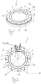
- FIGS. 1 and 2 illustrate an inventive vacuum clamping device in the form of a vacuum table 1 .
- a wafer 2 is clamped onto the vacuum table 1 , said wafer being supposed to be inspected visually.
- the vacuum table 1 comprises a base plate 3 which comprises a suction surface 4 .
- the base plate 3 is made of glass.
- the wafer 2 which rests on the base plate 3 is essentially circular, the wafer 2 being flat in one point 5 in order to be able to grip it more easily.
- a plurality of suction openings 6 is realized in the suction surface 4 of the base plate 3 .
- the suction openings 6 are disposed on an imaginary ring 6 a , which is flat in one point, in the suction surface 4 of the base plate 3 .
- this imaginary ring 6 a corresponds to the shape of the wafer 2 , said ring 6 a being slightly smaller than the wafer 2 so that the wafer 2 only, just covers the imaginary ring 6 a with the suction openings 6 . It can easily be seen in FIG. 8 that the suction openings 6 and the wafer 2 are disposed in this way. Here, the wafer is illustrated in a transparent way so that it can be illustrated more easily and so that the suction openings can be seen.
- the vacuum table 1 furthermore comprises an upper ring 7 , a holding ring 8 which is connected to the upper ring 7 and which serves to fix the base plate 3 , and a lower ring 9 .
- the rings 7 , 8 and 9 are made of aluminum and are connected via screw connections.
- FIGS. 1 and 2 show clearances 10 in the upper ring 7 for introducing fastening screws.
- the upper ring 7 comprises a plurality of indentations 19 . These indentations 19 serve to insert adjusting units which provide a certain amount of vertical movability of the rings 7 , 8 and 9 .
- the holding ring 8 is lifted slightly. This “open position” is illustrated in FIGS. 3 a , 4 a and 6 .
- FIGS. 3 b , 4 b and 5 illustrate the “closed position” in which the rings 8 and 9 rest one on top of the other.
- the holding ring 8 furthermore comprises an O-ring 20 which ensures the best possible sealing against the outside in the closed position of the vacuum table 1 .
- the lifting mechanism of the vacuum table 1 furthermore comprises a guide rod 11 and a ball lining 12 which is connected to the guide rod 11 .
- a cover 13 is provided at the upper end of the ball lining.
- a flexible glass film 14 is disposed between the base plate 3 and the wafer 2 , said glass film 14 comprising suction clearances.
- the suction clearances of the glass film 14 are disposed in such a way that they are disposed above the suction openings 6 in the suction surface 4 of the base plate 3 .
- the suction clearances in the glass film 14 are thus also disposed on an imaginary ring which is flat in one point. For fixing the glass film 14 , it is clamped between the upper ring 7 and the holding ring 8 .
- the vacuum table 1 On the lower side of the vacuum table 1 (i.e., the side facing away from the base plate 3 ), the vacuum table 1 is closed off against the outside by a cover plate 15 . In the closed position, the cover plate 15 ensures a hermetical sealing of the interior 16 between the base plate 3 and the cover plate 15 .
- the wafer 2 is initially placed on the base plate 3 with the help of a transport guiding blade (not illustrated) in such a way that the wafer 2 covers all suction openings 6 in the suction surface 4 of the base plate 3 .
- a transport guiding blade (not illustrated)
- the way in which the suction openings 6 are disposed in the base plate 3 corresponds to the shape of the wafer 2 , the wafer 2 being slightly larger than the imaginary flat ring 6 a on which the suction openings 6 are disposed.
- the glass film 14 is disposed between the wafer 2 and the base plate 3 , the suction clearances of said glass film 14 being positioned directly above the suction openings 6 in the base plate 3 .
- the vacuum table 1 is moved from the open position into the closed position by lowering the holding ring 8 onto the lower ring 9 .
- the glass film 14 and the holding ring 8 draw an angle of approximately 3°.
- an adaptation to the uneven wafer 2 is achieved.
- a sufficient vacuum can be built up faster between the wafer 2 and the glass film 14 .
- the way in which the glass film 14 is disposed can be seen in FIG. 10 .
- the air is now sucked off from the interior 16 via the vacuum connections 17 a and 17 b .
- At least one of the suction openings 6 is connected to a vacuum channel 18 which in turn has an open connection to one of the vacuum connections 17 a or 17 b . Due to the vacuum which is generated, the wafer 2 is initially pulled onto the glass film 14 in the region of the suction opening which is connected to the vacuum channel 18 . This is possible particularly easily since the suction clearances in the glass film 14 are positioned directly above the suction openings 6 so that the vacuum can take direct effect onto the wafer 2 in this manner. All suction openings 6 have an open connection.
- the suction openings 6 pervade the base plate 3 completely from its upper side up to its lower side, thereby being connected in an open way via the interior 16 . Due to the fact that the suction openings 6 have an open connection, the vacuum quickly spreads over all suction openings 6 so that the wafer is finally pulled onto the glass film 14 or the base plate 3 via all suction openings 6 .
- the wafer 2 acts as a kind of “lid” only with the aid of which it is possible in the first place to generate a vacuum between the wafer and the base plate 3 or the glass film 14 and to pull the wafer 2 smoothly onto the base plate 3 consequently. In this flat form, the wafer 2 can now be inspected visually in the best possible way.
- suction openings 6 Due to the fact that all of the suction openings 6 are disposed in a periphery region of the base plate 3 and in the outermost edge region of the wafer 2 to be inspected, these suction openings 6 do not hamper a visual inspection of the wafer 2 . This is why a visual inspection of the wafer 2 —except for the outermost edge region can be performed without any hampering shadows due to suction openings since there are no suction openings within the ring 6 a . It has also proven that by disposing the suction openings 6 in the outermost edge region of the wafer 2 to be inspected, a particularly strong vacuum can be generated by means of which an uneven wafer can be smoothed out firmly and safely.
- the wafer 2 has a diameter of 15 cm.
- the suction openings have a diameter of 0.5 mm.
Landscapes
- Engineering & Computer Science (AREA)
- Physics & Mathematics (AREA)
- Condensed Matter Physics & Semiconductors (AREA)
- General Physics & Mathematics (AREA)
- Manufacturing & Machinery (AREA)
- Computer Hardware Design (AREA)
- Microelectronics & Electronic Packaging (AREA)
- Power Engineering (AREA)
- Mechanical Engineering (AREA)
- Container, Conveyance, Adherence, Positioning, Of Wafer (AREA)
Applications Claiming Priority (3)
| Application Number | Priority Date | Filing Date | Title |
|---|---|---|---|
| DE102019112318.6 | 2019-05-10 | ||
| DE102019112318.6A DE102019112318B3 (de) | 2019-05-10 | 2019-05-10 | Vakuumspannvorrichtung |
| PCT/EP2020/062460 WO2020229233A1 (de) | 2019-05-10 | 2020-05-05 | Vakuumspannvorrichtung |
Publications (2)
| Publication Number | Publication Date |
|---|---|
| US20220216091A1 US20220216091A1 (en) | 2022-07-07 |
| US11804399B2 true US11804399B2 (en) | 2023-10-31 |
Family
ID=70554080
Family Applications (1)
| Application Number | Title | Priority Date | Filing Date |
|---|---|---|---|
| US17/610,093 Active 2040-08-18 US11804399B2 (en) | 2019-05-10 | 2020-05-05 | Vacuum clamping device |
Country Status (6)
| Country | Link |
|---|---|
| US (1) | US11804399B2 (de) |
| EP (1) | EP3966855B1 (de) |
| KR (1) | KR102694105B1 (de) |
| CN (1) | CN113826190B (de) |
| DE (1) | DE102019112318B3 (de) |
| WO (1) | WO2020229233A1 (de) |
Families Citing this family (2)
| Publication number | Priority date | Publication date | Assignee | Title |
|---|---|---|---|---|
| TWI769104B (zh) * | 2021-10-26 | 2022-06-21 | 毅力科技有限公司 | 壓膜裝置以及真空壓膜系統 |
| CN116613099B (zh) * | 2023-06-25 | 2024-07-26 | 浙江华企正邦自动化科技有限公司 | 一种蓝膜晶圆盘固定装置 |
Citations (7)
| Publication number | Priority date | Publication date | Assignee | Title |
|---|---|---|---|---|
| US5534073A (en) * | 1992-09-07 | 1996-07-09 | Mitsubishi Denki Kabushiki Kaisha | Semiconductor producing apparatus comprising wafer vacuum chucking device |
| US6032997A (en) * | 1998-04-16 | 2000-03-07 | Excimer Laser Systems | Vacuum chuck |
| US20080146124A1 (en) | 2006-12-13 | 2008-06-19 | Nec Electronics Corporation | Semiconductor manufacturing apparatus and semiconductor manufacturing method |
| US20120216396A1 (en) | 2011-02-28 | 2012-08-30 | Pradeep Kumar Rai | Non-uniform vacuum profile die attach tip |
| DE202013100632U1 (de) | 2013-02-13 | 2013-03-04 | Horst Witte Gerätebau Barskamp KG | Vakuumspannvorrichtung |
| CN104934356A (zh) | 2015-07-16 | 2015-09-23 | 北京工业大学 | 一种大尺寸晶圆真空吸盘 |
| US20180326590A1 (en) * | 2015-11-16 | 2018-11-15 | Takatori Corporation | Wire saw device, and processing method and processing device for workpiece |
Family Cites Families (6)
| Publication number | Priority date | Publication date | Assignee | Title |
|---|---|---|---|---|
| DE10161902B4 (de) | 2001-12-17 | 2005-06-23 | Infineon Technologies Ag | Verfahren und Vorrichtung zum Handhaben von Platten |
| JP2004228453A (ja) * | 2003-01-27 | 2004-08-12 | Renesas Technology Corp | 半導体装置の製造方法 |
| JP2009170730A (ja) | 2008-01-17 | 2009-07-30 | Fujifilm Corp | 裏面照射型固体撮像素子の検査装置 |
| DE102011075001A1 (de) * | 2011-04-29 | 2012-10-31 | 3D-Micromac Ag | Transluzenzvorrichtung zum Anhaften von Körpern |
| DE102014118830A1 (de) * | 2014-12-17 | 2016-06-23 | Mechatronic Systemtechnik Gmbh | Vakuumspannvorrichtung zum Aufspannen von Werkstücken |
| WO2019053752A1 (de) * | 2017-09-13 | 2019-03-21 | Esto Srl | Vakuumspann vorrichtung zum aufspannen von werkstücken mittels unterdruck |
-
2019
- 2019-05-10 DE DE102019112318.6A patent/DE102019112318B3/de active Active
-
2020
- 2020-05-05 CN CN202080035033.3A patent/CN113826190B/zh active Active
- 2020-05-05 EP EP20724089.6A patent/EP3966855B1/de active Active
- 2020-05-05 WO PCT/EP2020/062460 patent/WO2020229233A1/de not_active Ceased
- 2020-05-05 KR KR1020217038271A patent/KR102694105B1/ko active Active
- 2020-05-05 US US17/610,093 patent/US11804399B2/en active Active
Patent Citations (7)
| Publication number | Priority date | Publication date | Assignee | Title |
|---|---|---|---|---|
| US5534073A (en) * | 1992-09-07 | 1996-07-09 | Mitsubishi Denki Kabushiki Kaisha | Semiconductor producing apparatus comprising wafer vacuum chucking device |
| US6032997A (en) * | 1998-04-16 | 2000-03-07 | Excimer Laser Systems | Vacuum chuck |
| US20080146124A1 (en) | 2006-12-13 | 2008-06-19 | Nec Electronics Corporation | Semiconductor manufacturing apparatus and semiconductor manufacturing method |
| US20120216396A1 (en) | 2011-02-28 | 2012-08-30 | Pradeep Kumar Rai | Non-uniform vacuum profile die attach tip |
| DE202013100632U1 (de) | 2013-02-13 | 2013-03-04 | Horst Witte Gerätebau Barskamp KG | Vakuumspannvorrichtung |
| CN104934356A (zh) | 2015-07-16 | 2015-09-23 | 北京工业大学 | 一种大尺寸晶圆真空吸盘 |
| US20180326590A1 (en) * | 2015-11-16 | 2018-11-15 | Takatori Corporation | Wire saw device, and processing method and processing device for workpiece |
Non-Patent Citations (1)
| Title |
|---|
| PCT International Search Report and Written Opinion, PCT/EP2020/062460, dated Aug. 3, 2020, 14 pages. |
Also Published As
| Publication number | Publication date |
|---|---|
| KR102694105B1 (ko) | 2024-08-09 |
| EP3966855A1 (de) | 2022-03-16 |
| CN113826190B (zh) | 2025-05-20 |
| US20220216091A1 (en) | 2022-07-07 |
| WO2020229233A1 (de) | 2020-11-19 |
| EP3966855C0 (de) | 2025-10-22 |
| KR20220017401A (ko) | 2022-02-11 |
| DE102019112318B3 (de) | 2020-07-23 |
| CN113826190A (zh) | 2021-12-21 |
| EP3966855B1 (de) | 2025-10-22 |
Similar Documents
| Publication | Publication Date | Title |
|---|---|---|
| US11804399B2 (en) | Vacuum clamping device | |
| US9381577B2 (en) | Chuck table | |
| US9636844B2 (en) | Cutting apparatus | |
| TWI730150B (zh) | 工作夾台、多孔陶瓷吸引板的製造方法及吸引保持系統 | |
| US9314853B2 (en) | Cutting apparatus | |
| TW201738950A (zh) | 晶圓之加工方法 | |
| US10832888B2 (en) | Ion milling apparatus and sample holder | |
| CN107924799B (zh) | 带电粒子显微镜的观察辅助单元以及使用该观察辅助单元的试料观察方法 | |
| JPWO2021171492A5 (de) | ||
| JP2007055197A (ja) | 脆性材料の割断装置 | |
| TW201912060A (zh) | 夾具 | |
| US8941916B2 (en) | Filter holder for correlative particle analysis | |
| US4146262A (en) | Device for taking-off slices | |
| US20160148779A1 (en) | Specimen Preparation Device | |
| CN212844589U (zh) | 用于聚焦离子束制样的样品台和具有其的制样设备 | |
| KR102069061B1 (ko) | 플렉시블 oled 셀의 영상 획득 시스템 | |
| JPH06325996A (ja) | レティクルフレーム | |
| JP5467816B2 (ja) | 撮像装置 | |
| CN217846086U (zh) | 一种打光装置 | |
| CN217820063U (zh) | 检测装置 | |
| US12340971B2 (en) | Microscope stage fixture for horizontal rotation | |
| JP2021040013A (ja) | カーフの認識方法 | |
| KR101727729B1 (ko) | 진공척 | |
| JP6014386B2 (ja) | ガラス板の照明装置及び加工装置 | |
| CN210666291U (zh) | 病理标本摄影及取材装置 |
Legal Events
| Date | Code | Title | Description |
|---|---|---|---|
| FEPP | Fee payment procedure |
Free format text: ENTITY STATUS SET TO UNDISCOUNTED (ORIGINAL EVENT CODE: BIG.); ENTITY STATUS OF PATENT OWNER: SMALL ENTITY |
|
| FEPP | Fee payment procedure |
Free format text: ENTITY STATUS SET TO SMALL (ORIGINAL EVENT CODE: SMAL); ENTITY STATUS OF PATENT OWNER: SMALL ENTITY |
|
| AS | Assignment |
Owner name: WITRINS S.R.O., CZECH REPUBLIC Free format text: ASSIGNMENT OF ASSIGNORS INTEREST;ASSIGNOR:WIESER, ROMAN FRANZ;REEL/FRAME:058283/0575 Effective date: 20211203 |
|
| STPP | Information on status: patent application and granting procedure in general |
Free format text: DOCKETED NEW CASE - READY FOR EXAMINATION |
|
| STPP | Information on status: patent application and granting procedure in general |
Free format text: NON FINAL ACTION MAILED |
|
| STPP | Information on status: patent application and granting procedure in general |
Free format text: NOTICE OF ALLOWANCE MAILED -- APPLICATION RECEIVED IN OFFICE OF PUBLICATIONS |
|
| STPP | Information on status: patent application and granting procedure in general |
Free format text: PUBLICATIONS -- ISSUE FEE PAYMENT VERIFIED |
|
| STCF | Information on status: patent grant |
Free format text: PATENTED CASE |