US11747685B2 - Display device, manufacturing method thereof, and multi-display device - Google Patents
Display device, manufacturing method thereof, and multi-display device Download PDFInfo
- Publication number
- US11747685B2 US11747685B2 US16/879,673 US202016879673A US11747685B2 US 11747685 B2 US11747685 B2 US 11747685B2 US 202016879673 A US202016879673 A US 202016879673A US 11747685 B2 US11747685 B2 US 11747685B2
- Authority
- US
- United States
- Prior art keywords
- base substrate
- conductive layers
- disposed
- gate
- electrically connected
- Prior art date
- Legal status (The legal status is an assumption and is not a legal conclusion. Google has not performed a legal analysis and makes no representation as to the accuracy of the status listed.)
- Active, expires
Links
Images


Classifications
-
- H—ELECTRICITY
- H05—ELECTRIC TECHNIQUES NOT OTHERWISE PROVIDED FOR
- H05K—PRINTED CIRCUITS; CASINGS OR CONSTRUCTIONAL DETAILS OF ELECTRIC APPARATUS; MANUFACTURE OF ASSEMBLAGES OF ELECTRICAL COMPONENTS
- H05K3/00—Apparatus or processes for manufacturing printed circuits
- H05K3/30—Assembling printed circuits with electric components, e.g. with resistors
- H05K3/32—Assembling printed circuits with electric components, e.g. with resistors electrically connecting electric components or wires to printed circuits
- H05K3/34—Assembling printed circuits with electric components, e.g. with resistors electrically connecting electric components or wires to printed circuits by soldering
- H05K3/3405—Edge mounted components, e.g. terminals
-
- G—PHYSICS
- G02—OPTICS
- G02F—OPTICAL DEVICES OR ARRANGEMENTS FOR THE CONTROL OF LIGHT BY MODIFICATION OF THE OPTICAL PROPERTIES OF THE MEDIA OF THE ELEMENTS INVOLVED THEREIN; NON-LINEAR OPTICS; FREQUENCY-CHANGING OF LIGHT; OPTICAL LOGIC ELEMENTS; OPTICAL ANALOGUE/DIGITAL CONVERTERS
- G02F1/00—Devices or arrangements for the control of the intensity, colour, phase, polarisation or direction of light arriving from an independent light source, e.g. switching, gating or modulating; Non-linear optics
- G02F1/01—Devices or arrangements for the control of the intensity, colour, phase, polarisation or direction of light arriving from an independent light source, e.g. switching, gating or modulating; Non-linear optics for the control of the intensity, phase, polarisation or colour
- G02F1/13—Devices or arrangements for the control of the intensity, colour, phase, polarisation or direction of light arriving from an independent light source, e.g. switching, gating or modulating; Non-linear optics for the control of the intensity, phase, polarisation or colour based on liquid crystals, e.g. single liquid crystal display cells
- G02F1/133—Constructional arrangements; Operation of liquid crystal cells; Circuit arrangements
- G02F1/1333—Constructional arrangements; Manufacturing methods
- G02F1/1345—Conductors connecting electrodes to cell terminals
- G02F1/13452—Conductors connecting driver circuitry and terminals of panels
-
- G—PHYSICS
- G02—OPTICS
- G02F—OPTICAL DEVICES OR ARRANGEMENTS FOR THE CONTROL OF LIGHT BY MODIFICATION OF THE OPTICAL PROPERTIES OF THE MEDIA OF THE ELEMENTS INVOLVED THEREIN; NON-LINEAR OPTICS; FREQUENCY-CHANGING OF LIGHT; OPTICAL LOGIC ELEMENTS; OPTICAL ANALOGUE/DIGITAL CONVERTERS
- G02F1/00—Devices or arrangements for the control of the intensity, colour, phase, polarisation or direction of light arriving from an independent light source, e.g. switching, gating or modulating; Non-linear optics
- G02F1/01—Devices or arrangements for the control of the intensity, colour, phase, polarisation or direction of light arriving from an independent light source, e.g. switching, gating or modulating; Non-linear optics for the control of the intensity, phase, polarisation or colour
- G02F1/13—Devices or arrangements for the control of the intensity, colour, phase, polarisation or direction of light arriving from an independent light source, e.g. switching, gating or modulating; Non-linear optics for the control of the intensity, phase, polarisation or colour based on liquid crystals, e.g. single liquid crystal display cells
- G02F1/133—Constructional arrangements; Operation of liquid crystal cells; Circuit arrangements
- G02F1/13306—Circuit arrangements or driving methods for the control of single liquid crystal cells
-
- G—PHYSICS
- G02—OPTICS
- G02F—OPTICAL DEVICES OR ARRANGEMENTS FOR THE CONTROL OF LIGHT BY MODIFICATION OF THE OPTICAL PROPERTIES OF THE MEDIA OF THE ELEMENTS INVOLVED THEREIN; NON-LINEAR OPTICS; FREQUENCY-CHANGING OF LIGHT; OPTICAL LOGIC ELEMENTS; OPTICAL ANALOGUE/DIGITAL CONVERTERS
- G02F1/00—Devices or arrangements for the control of the intensity, colour, phase, polarisation or direction of light arriving from an independent light source, e.g. switching, gating or modulating; Non-linear optics
- G02F1/01—Devices or arrangements for the control of the intensity, colour, phase, polarisation or direction of light arriving from an independent light source, e.g. switching, gating or modulating; Non-linear optics for the control of the intensity, phase, polarisation or colour
- G02F1/13—Devices or arrangements for the control of the intensity, colour, phase, polarisation or direction of light arriving from an independent light source, e.g. switching, gating or modulating; Non-linear optics for the control of the intensity, phase, polarisation or colour based on liquid crystals, e.g. single liquid crystal display cells
- G02F1/133—Constructional arrangements; Operation of liquid crystal cells; Circuit arrangements
- G02F1/1333—Constructional arrangements; Manufacturing methods
- G02F1/13336—Combining plural substrates to produce large-area displays, e.g. tiled displays
-
- G—PHYSICS
- G02—OPTICS
- G02F—OPTICAL DEVICES OR ARRANGEMENTS FOR THE CONTROL OF LIGHT BY MODIFICATION OF THE OPTICAL PROPERTIES OF THE MEDIA OF THE ELEMENTS INVOLVED THEREIN; NON-LINEAR OPTICS; FREQUENCY-CHANGING OF LIGHT; OPTICAL LOGIC ELEMENTS; OPTICAL ANALOGUE/DIGITAL CONVERTERS
- G02F1/00—Devices or arrangements for the control of the intensity, colour, phase, polarisation or direction of light arriving from an independent light source, e.g. switching, gating or modulating; Non-linear optics
- G02F1/01—Devices or arrangements for the control of the intensity, colour, phase, polarisation or direction of light arriving from an independent light source, e.g. switching, gating or modulating; Non-linear optics for the control of the intensity, phase, polarisation or colour
- G02F1/13—Devices or arrangements for the control of the intensity, colour, phase, polarisation or direction of light arriving from an independent light source, e.g. switching, gating or modulating; Non-linear optics for the control of the intensity, phase, polarisation or colour based on liquid crystals, e.g. single liquid crystal display cells
- G02F1/133—Constructional arrangements; Operation of liquid crystal cells; Circuit arrangements
- G02F1/1333—Constructional arrangements; Manufacturing methods
- G02F1/1345—Conductors connecting electrodes to cell terminals
-
- G—PHYSICS
- G02—OPTICS
- G02F—OPTICAL DEVICES OR ARRANGEMENTS FOR THE CONTROL OF LIGHT BY MODIFICATION OF THE OPTICAL PROPERTIES OF THE MEDIA OF THE ELEMENTS INVOLVED THEREIN; NON-LINEAR OPTICS; FREQUENCY-CHANGING OF LIGHT; OPTICAL LOGIC ELEMENTS; OPTICAL ANALOGUE/DIGITAL CONVERTERS
- G02F1/00—Devices or arrangements for the control of the intensity, colour, phase, polarisation or direction of light arriving from an independent light source, e.g. switching, gating or modulating; Non-linear optics
- G02F1/01—Devices or arrangements for the control of the intensity, colour, phase, polarisation or direction of light arriving from an independent light source, e.g. switching, gating or modulating; Non-linear optics for the control of the intensity, phase, polarisation or colour
- G02F1/13—Devices or arrangements for the control of the intensity, colour, phase, polarisation or direction of light arriving from an independent light source, e.g. switching, gating or modulating; Non-linear optics for the control of the intensity, phase, polarisation or colour based on liquid crystals, e.g. single liquid crystal display cells
- G02F1/133—Constructional arrangements; Operation of liquid crystal cells; Circuit arrangements
- G02F1/136—Liquid crystal cells structurally associated with a semi-conducting layer or substrate, e.g. cells forming part of an integrated circuit
- G02F1/1362—Active matrix addressed cells
- G02F1/136286—Wiring, e.g. gate line, drain line
-
- G—PHYSICS
- G09—EDUCATION; CRYPTOGRAPHY; DISPLAY; ADVERTISING; SEALS
- G09G—ARRANGEMENTS OR CIRCUITS FOR CONTROL OF INDICATING DEVICES USING STATIC MEANS TO PRESENT VARIABLE INFORMATION
- G09G3/00—Control arrangements or circuits, of interest only in connection with visual indicators other than cathode-ray tubes
- G09G3/20—Control arrangements or circuits, of interest only in connection with visual indicators other than cathode-ray tubes for presentation of an assembly of a number of characters, e.g. a page, by composing the assembly by combination of individual elements arranged in a matrix no fixed position being assigned to or needed to be assigned to the individual characters or partial characters
- G09G3/34—Control arrangements or circuits, of interest only in connection with visual indicators other than cathode-ray tubes for presentation of an assembly of a number of characters, e.g. a page, by composing the assembly by combination of individual elements arranged in a matrix no fixed position being assigned to or needed to be assigned to the individual characters or partial characters by control of light from an independent source
- G09G3/36—Control arrangements or circuits, of interest only in connection with visual indicators other than cathode-ray tubes for presentation of an assembly of a number of characters, e.g. a page, by composing the assembly by combination of individual elements arranged in a matrix no fixed position being assigned to or needed to be assigned to the individual characters or partial characters by control of light from an independent source using liquid crystals
- G09G3/3611—Control of matrices with row and column drivers
- G09G3/3696—Generation of voltages supplied to electrode drivers
-
- H01L27/124—
-
- H01L27/1259—
-
- H—ELECTRICITY
- H05—ELECTRIC TECHNIQUES NOT OTHERWISE PROVIDED FOR
- H05K—PRINTED CIRCUITS; CASINGS OR CONSTRUCTIONAL DETAILS OF ELECTRIC APPARATUS; MANUFACTURE OF ASSEMBLAGES OF ELECTRICAL COMPONENTS
- H05K1/00—Printed circuits
- H05K1/18—Printed circuits structurally associated with non-printed electric components
- H05K1/189—Printed circuits structurally associated with non-printed electric components characterised by the use of flexible or folded printed circuits
-
- H—ELECTRICITY
- H05—ELECTRIC TECHNIQUES NOT OTHERWISE PROVIDED FOR
- H05K—PRINTED CIRCUITS; CASINGS OR CONSTRUCTIONAL DETAILS OF ELECTRIC APPARATUS; MANUFACTURE OF ASSEMBLAGES OF ELECTRICAL COMPONENTS
- H05K3/00—Apparatus or processes for manufacturing printed circuits
- H05K3/30—Assembling printed circuits with electric components, e.g. with resistors
- H05K3/303—Assembling printed circuits with electric components, e.g. with resistors with surface mounted components
-
- H—ELECTRICITY
- H10—SEMICONDUCTOR DEVICES; ELECTRIC SOLID-STATE DEVICES NOT OTHERWISE PROVIDED FOR
- H10D—INORGANIC ELECTRIC SEMICONDUCTOR DEVICES
- H10D86/00—Integrated devices formed in or on insulating or conducting substrates, e.g. formed in silicon-on-insulator [SOI] substrates or on stainless steel or glass substrates
- H10D86/01—Manufacture or treatment
- H10D86/021—Manufacture or treatment of multiple TFTs
-
- H—ELECTRICITY
- H10—SEMICONDUCTOR DEVICES; ELECTRIC SOLID-STATE DEVICES NOT OTHERWISE PROVIDED FOR
- H10D—INORGANIC ELECTRIC SEMICONDUCTOR DEVICES
- H10D86/00—Integrated devices formed in or on insulating or conducting substrates, e.g. formed in silicon-on-insulator [SOI] substrates or on stainless steel or glass substrates
- H10D86/40—Integrated devices formed in or on insulating or conducting substrates, e.g. formed in silicon-on-insulator [SOI] substrates or on stainless steel or glass substrates characterised by multiple TFTs
- H10D86/441—Interconnections, e.g. scanning lines
-
- H—ELECTRICITY
- H10—SEMICONDUCTOR DEVICES; ELECTRIC SOLID-STATE DEVICES NOT OTHERWISE PROVIDED FOR
- H10D—INORGANIC ELECTRIC SEMICONDUCTOR DEVICES
- H10D86/00—Integrated devices formed in or on insulating or conducting substrates, e.g. formed in silicon-on-insulator [SOI] substrates or on stainless steel or glass substrates
- H10D86/40—Integrated devices formed in or on insulating or conducting substrates, e.g. formed in silicon-on-insulator [SOI] substrates or on stainless steel or glass substrates characterised by multiple TFTs
- H10D86/60—Integrated devices formed in or on insulating or conducting substrates, e.g. formed in silicon-on-insulator [SOI] substrates or on stainless steel or glass substrates characterised by multiple TFTs wherein the TFTs are in active matrices
-
- G—PHYSICS
- G02—OPTICS
- G02F—OPTICAL DEVICES OR ARRANGEMENTS FOR THE CONTROL OF LIGHT BY MODIFICATION OF THE OPTICAL PROPERTIES OF THE MEDIA OF THE ELEMENTS INVOLVED THEREIN; NON-LINEAR OPTICS; FREQUENCY-CHANGING OF LIGHT; OPTICAL LOGIC ELEMENTS; OPTICAL ANALOGUE/DIGITAL CONVERTERS
- G02F1/00—Devices or arrangements for the control of the intensity, colour, phase, polarisation or direction of light arriving from an independent light source, e.g. switching, gating or modulating; Non-linear optics
- G02F1/01—Devices or arrangements for the control of the intensity, colour, phase, polarisation or direction of light arriving from an independent light source, e.g. switching, gating or modulating; Non-linear optics for the control of the intensity, phase, polarisation or colour
- G02F1/13—Devices or arrangements for the control of the intensity, colour, phase, polarisation or direction of light arriving from an independent light source, e.g. switching, gating or modulating; Non-linear optics for the control of the intensity, phase, polarisation or colour based on liquid crystals, e.g. single liquid crystal display cells
- G02F1/133—Constructional arrangements; Operation of liquid crystal cells; Circuit arrangements
- G02F1/136—Liquid crystal cells structurally associated with a semi-conducting layer or substrate, e.g. cells forming part of an integrated circuit
- G02F1/1362—Active matrix addressed cells
- G02F1/136286—Wiring, e.g. gate line, drain line
- G02F1/136295—Materials; Compositions; Manufacture processes
-
- H—ELECTRICITY
- H05—ELECTRIC TECHNIQUES NOT OTHERWISE PROVIDED FOR
- H05K—PRINTED CIRCUITS; CASINGS OR CONSTRUCTIONAL DETAILS OF ELECTRIC APPARATUS; MANUFACTURE OF ASSEMBLAGES OF ELECTRICAL COMPONENTS
- H05K2201/00—Indexing scheme relating to printed circuits covered by H05K1/00
- H05K2201/04—Assemblies of printed circuits
- H05K2201/049—PCB for one component, e.g. for mounting onto mother PCB
-
- H—ELECTRICITY
- H05—ELECTRIC TECHNIQUES NOT OTHERWISE PROVIDED FOR
- H05K—PRINTED CIRCUITS; CASINGS OR CONSTRUCTIONAL DETAILS OF ELECTRIC APPARATUS; MANUFACTURE OF ASSEMBLAGES OF ELECTRICAL COMPONENTS
- H05K2201/00—Indexing scheme relating to printed circuits covered by H05K1/00
- H05K2201/10—Details of components or other objects attached to or integrated in a printed circuit board
- H05K2201/10007—Types of components
- H05K2201/10128—Display
- H05K2201/10136—Liquid Crystal display [LCD]
-
- H—ELECTRICITY
- H05—ELECTRIC TECHNIQUES NOT OTHERWISE PROVIDED FOR
- H05K—PRINTED CIRCUITS; CASINGS OR CONSTRUCTIONAL DETAILS OF ELECTRIC APPARATUS; MANUFACTURE OF ASSEMBLAGES OF ELECTRICAL COMPONENTS
- H05K2203/00—Indexing scheme relating to apparatus or processes for manufacturing printed circuits covered by H05K3/00
- H05K2203/10—Using electric, magnetic and electromagnetic fields; Using laser light
- H05K2203/107—Using laser light
-
- H—ELECTRICITY
- H05—ELECTRIC TECHNIQUES NOT OTHERWISE PROVIDED FOR
- H05K—PRINTED CIRCUITS; CASINGS OR CONSTRUCTIONAL DETAILS OF ELECTRIC APPARATUS; MANUFACTURE OF ASSEMBLAGES OF ELECTRICAL COMPONENTS
- H05K3/00—Apparatus or processes for manufacturing printed circuits
- H05K3/36—Assembling printed circuits with other printed circuits
- H05K3/366—Assembling printed circuits with other printed circuits substantially perpendicularly to each other
Definitions
- the technical field relates to a display device, a manufacturing method thereof, and a related multi-display device.
- a display device in general, includes a display panel including a plurality of pixels for displaying an image, includes a gate driver for providing gate signals to the pixels, and includes a data driver for providing data voltages to the pixels.
- the gate driver and the data driver are connected to the display panel.
- the gate driver generates gate signals and provides the generated gate signals to the pixels.
- the data driver generates data voltages and provides the generated data voltages to the pixels.
- the pixels receive the data voltages and display an image in response to the gate signals.
- the gate driver and the data driver may be disposed in a bezel area. In general, it is desirable to minimize the bezel area.
- Embodiments may be related to a display device having a narrow bezel, a related manufacturing method, and a related multi-display device.
- An embodiment may be related to a display device including the following elements: a first substrate; a second substrate disposed on the first substrate; an image display layer disposed between the first substrate and the second substrate; a gate driver disposed at a first side surface of the first substrate; a data driver disposed at a second side surface of the first substrate; and a plurality of first conductive layers disposed in first recessed portions defined in the first side surface.
- the gate driver is connected to the first conductive layers.
- a method for manufacturing a display device includes the following steps: defining first recessed portions in a first side surface of a first substrate; defining second recessed portions in a second side surface of a first substrate; providing a plurality of first conductive layers in the first recessed portions; providing a plurality of second conductive layers in the second recessed portions; connecting a gate driver to the first conductive layers; and connecting a data driver to the second conductive layers.
- a multi-display device includes a plurality of display panels connected to each other.
- Each of the display panels includes the following elements: a first substrate; a second substrate disposed on the first substrate; an image display layer disposed between the first substrate and the second substrate; a gate driver disposed at a first side surface of the first substrate; a data driver disposed at a second side surface of the first substrate; a plurality of first conductive layers disposed in first recessed portions defined in the first side surface; and a plurality of second conductive layers disposed in second recessed portions defined in the second side surface.
- the gate driver is connected to the first conductive layers
- the data driver is connected to the second conductive layers
- a first side surface of a k-th display panel and a first side surface of a k+1-th display panel of the display panels face each other.
- An embodiment may be related to a display device.
- the display device may include a first base substrate, a second base substrate overlapping the first base substrate, an image display layer disposed between the first base substrate and the second base substrate, a gate driver disposed at a first side surface of the first base substrate, a data driver disposed at a second side surface of the first base substrate, and first conductive layers respectively disposed in first recesses recessed from the first side surface of the first base substrate.
- the gate driver may be electrically connected to the first conductive layers.
- the second side surface of the first base substrate may extend lengthwise in a first direction.
- the first side surface of the first base substrate may extend lengthwise in a second direction different from the first direction.
- the first recesses may be arranged in the second direction and have respective depths in the first direction.
- the display device may include the following elements: gate lines extending lengthwise individually in the first direction, overlapping the first base substrate, and respectively electrically connected to the first conductive layers; data lines extending lengthwise individually in the second direction, electrically insulated from the gate lines, and overlapping the first base substrate; and pixels electrically connected to the gate lines and the data lines.
- Each of the first conductive layers may be wider than each of the gate lines in the second direction.
- the gate driver may include the following elements: a first flexible circuit board; a first driving chip mounted to the first flexible circuit board; and first pads disposed on the first flexible circuit board, electrically connected to the first driving chip, and respectively electrically connected to the first conductive layers.
- the first flexible circuit board may overlap the first side surface of the first base substrate.
- the display device may include second conductive layers respectively disposed in second recesses recessed from the second side surface of the first base substrate.
- the second recesses may be arranged in the first direction and have respective depths in the second direction.
- the data driver may be electrically connected to the second conductive layers.
- the data lines may be respectively electrically connected to the second conductive layers.
- the display device may include connection electrodes disposed between the second conductive layers and the data lines to electrically connect the data lines and the second conductive layers.
- Each of the second conductive layers and each of the connection electrodes may be wider than each of the data lines in the first direction.
- Faces of the connection electrodes may be coplanar with faces of the gate lines.
- the data driver may include the following elements: a second flexible circuit board; a second driving chip mounted to the second flexible circuit board; and second pads disposed on the second flexible circuit board, electrically connected to the second driving chip, and respectively electrically connected to the second conductive layers.
- the second flexible circuit board may overlap the second side surface of the first base substrate.
- An embodiment may be related to a method for manufacturing a display device.
- the method may include the following steps: preparing first recesses that are recessed from a first side surface of a first base substrate; preparing second recesses that are recessed from a second side surface of the first base substrate; providing first conductive layers in the first recesses, respectively; providing second conductive layers in the second recesses, respectively; electrically connecting a gate driver to the first conductive layers; and electrically connecting a data driver to the second conductive layers.
- the preparing of the first and second recesses may include irradiating a laser toward at least one of the first surface of a first base substrate and the second side surface of a first base substrate.
- the method may include the following steps: providing gate lines disposed on the first base substrate, each of the gate lines extending in a first direction; providing an insulation layer on the first base substrate to cover the gate lines; and providing data lines on the insulation layer, each of the data lines extending in a second direction different from the first direction.
- the second side surface of the first base substrate may extend lengthwise in the first direction.
- the first side surface of the first base substrate may extend lengthwise in the second direction.
- the first recesses may have respective depths in the first direction.
- the second recesses may have respective depths in the second direction.
- the gate lines may be respectively electrically connected to the first conductive layers.
- the data lines may be respectively electrically connected to the second conductive layers.
- the gate driver may include the following elements: a first flexible circuit board; a first driving chip mounted to the first flexible circuit board; and first pads disposed on the first flexible circuit board, electrically connected to the first driving chip, and respectively electrically connected to the first conductive layers.
- the data driver may include the following elements: a second flexible circuit board; a second driving chip mounted to the second flexible circuit board; and second pads disposed the second flexible circuit board, electrically connected to the second driving chip, and respectively electrically connected to the second conductive layers.
- the preparing of the first recesses may include irradiating a first laser toward a first portion of a face of the first base substrate.
- the first portion of the face of the first base substrate may be adjacent to the first side surface of the first base substrate.
- the preparing of the second recesses may include irradiating the first laser or a second laser toward a second portion of the face of the first base substrate.
- the second portion of the face of the first base substrate may be adjacent to the second side surface of the first base substrate.
- the method may include the following steps: providing gate lines and connection electrodes on the first base substrate, wherein the gate lines may be respectively electrically connected to the first conductive layers, and wherein the connection electrodes may be respectively electrically connected to the second conductive layers; providing an insulation layer on the first base substrate to cover the gate lines and the connection electrodes; and providing data lines on the insulation layer, wherein the data lines may be respectively electrically connected to the connection electrodes through first contact holes provided in the insulation layer.
- An embodiment may be related to a multi-display device that includes a plurality of display panels connected to each other.
- Each of the display panels may include a first base substrate, a second substrate overlapping the first base substrate, an image display layer disposed between the first base substrate and the second base substrate, a gate driver disposed at a first side surface of the first base substrate, a data driver disposed at a second side surface of the first base substrate, first conductive layers respectively disposed in first recesses recessed from the first side surface, and second conductive layers respectively disposed in second recesses recessed from the second side surface.
- the gate driver may be electrically connected to the first conductive layers.
- the data driver may be electrically connected to the second conductive layers.
- the first side surfaces of the first base substrates of two immediately neighboring ones of the display panels may face each other.
- FIG. 1 is a plan view illustrating a display device according to an embodiment.
- FIG. 2 is a perspective view illustrating the display device in FIG. 1 according to an embodiment.
- FIG. 3 is a view illustrating a configuration of one pixel in FIG. 1 according to an embodiment.
- FIG. 4 is a schematic view illustrating a cross-section of the pixel in FIG. 3 according to an embodiment.
- FIG. 5 is a view illustrating a portion of a first side surface on which a first gate driver is disposed according to an embodiment.
- FIG. 6 is a cross-sectional view taken along line I-I′ of FIG. 5 according to an embodiment.
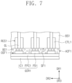
- FIG. 7 is a view illustrating a connection state between first pads and first conductive layers according to an embodiment.
- FIG. 8 is a view illustrating a portion of a second side surface on which a data driver is disposed according to an embodiment.
- FIG. 9 is a cross-sectional view taken along line II-II′ of FIG. 8 according to an embodiment.
- FIG. 10 is a view illustrating a connection state between second pads and second conductive layers according to an embodiment.
- FIG. 11 , FIG. 12 , FIG. 13 , FIG. 14 , FIG. 15 , and FIG. 16 are views illustrating structures formed in a method for manufacturing the display device according to an embodiment.
- FIG. 17 , FIG. 18 , FIG. 19 , FIG. 20 , FIG. 21 , FIG. 22 , and FIG. 23 are views illustrating structures formed in a method for manufacturing a display device according to another embodiment.
- FIG. 24 is a view illustrating a multi-display device according to an embodiment.
- FIG. 25 is a cross-sectional view taken along line III-III′ of FIG. 24 according to an embodiment.
- first,” “second,” etc. may be used to describe various elements, these elements should not be limited by these terms. These terms may be used to distinguish one element from another element. A first element may be termed a second element without departing from teachings of one or more embodiments. The description of an element as a “first” element may not require or imply the presence of a second element or other elements. The terms “first,” “second,” etc. may be used to differentiate different categories or sets of elements. For conciseness, the terms “first,” “second,” etc. may represent “first-type (or first-set),” “second-type (or second-set),” etc., respectively.
- first element When a first element is referred to as being ‘on,’ ‘connected to,’ or ‘coupled to,’ a second element, the first element can be directly disposed/connected/coupled on/to the second element, or an intervening element may be present between the first element and the second element.
- connection may mean “electrically connect.”
- insulate may mean “electrically insulate” or “electrically isolate.”
- extend may mean “extend lengthwise” or “be lengthwise.”
- recessed portion may mean “recess.”
- contact may mean “directly contact.”
- FIG. 1 is a plan view illustrating a display device according to an embodiment.
- a display device DD may include a display panel DP, gate drivers GDR 1 and GDR 2 , a data driver DDR, and a printed circuit board PCB.
- the display panel DP may have a rectangular shape having long sides extending in a first direction DR 1 and short sides extending in a second direction DR 2 crossing the first direction DR 1 .
- the display device DD may have one or more other shapes.
- a direction that is substantially perpendicular to a plane defined by the directions DR 1 and DR 2 is defined as a third direction DR 3 .
- a plan view may represent a view in the third direction DR 3 .
- the display panel DP may be a liquid crystal display panel including a liquid crystal layer.
- the display panel DP may be an electrophoretic display panel including an electrophoretic layer or an electrowetting display panel including an electrowetting layer.
- Each of the liquid crystal layer, the electrophoretic layer, and the electrowetting layer may be an image display layer.
- the display panel DP may include a plurality of pixels PX, a plurality of gate lines GL 1 to GLm, and a plurality of data lines DL 1 to DLn.
- reference numerals m and n are natural numbers.
- the gate lines GL 1 to GLm may cross the data lines DL 1 to DLn and may be insulated from the data lines DL 1 to DLn.
- the pixels PX are connected to the gate lines GL 1 to GLm and the data lines DL 1 to DLn.
- Each of the pixels PX may display one of primary colors.
- the primary colors may include red, green, blue, and white.
- the primary colors may include yellow, cyan, and magenta.
- Each of the gate lines GL 1 to GLm may extend in the first direction DR 1
- each of the data lines DL 1 to DLn may extend in the second direction DR 2 .
- the gate drivers GDR 1 and GDR 2 may be connected to the display panel DP and connected to the gate lines GL 1 to GLm.
- the data driver DDR may be connected to the display panel DP and then connected to the data lines DL 1 to DLn.
- the gate drivers GDR 1 and GDR 2 and the data driver DDR are separately illustrated for convenience.
- the gate drivers GDR 1 and GDR 2 and the data driver DDR may be connected to the display panel DP.
- the gate drivers GDR 1 and GDR 2 may include a first gate driver GDR 1 and a second gate driver GDR 2 , which are respectively adjacent to two sides of the display panel DP that are opposite each other in the first direction DR 1 .
- the gate drivers GDR 1 and GDR 2 may be adjacent to the short sides of the display panel DP, respectively.
- the first gate driver GDR 1 may be connected to odd-numbered gate lines of the gate lines GL 1 to GLm.
- the second gate driver GDR 2 may be connected to even-numbered gate lines of the gate lines GL 1 to GLm.
- One gate driver GDR 1 and GDR 2 are illustrated.
- one gate driver may be disposed at one side of the display panel DP and connected to the gate lines GL 1 to GLm.
- Each of the gate drivers GDR 1 and GDR 2 may include first flexible circuit boards FPC 1 and first driving chips IC 1 mounted to the first flexible circuit boards FPC 1 , respectively.
- the first driving chips ICI may be connected to the display panel DP through the first flexible circuit boards FPC 1 .
- the first driving chips IC 1 of the first gate driver GDR 1 may be connected to the odd-numbered gate lines through the first flexible circuit boards FPC 1 of the first gate driver GDR 1 .
- the first driving chips IC 1 of the second gate driver GDR 2 may be connected to the even-numbered gate lines through the first flexible circuit boards FPC 1 of the second gate driver GDR 2 .
- Each of the first and second gate drivers GDR 1 and GDR 2 includes four first driving chips IC 1 and four first flexible circuit boards FPC 1 in FIG. 1 .
- the number of the first driving chips IC 1 and the number of the first flexible circuit boards FPC 1 may be configured according to a size of the display panel DP.
- the data driver DDR may be adjacent to one side of the display panel DP that is lengthwise in the first direction DR 1 .
- the data driver DDR may be adjacent to one of the long sides of the display panel DP.
- the data driver DDR may include second flexible circuit boards FPC 2 and second driving chips IC 2 mounted to the second flexible circuit boards FPC 2 , respectively.
- the second driving chips IC 2 may be connected to the display panel DP through the second flexible circuit boards FPC 2 .
- FIG. 1 Five second driving chips IC 2 and five second flexible circuit boards FPC 2 are illustrated in FIG. 1 .
- the number of the second driving chips IC 2 and the number of the second flexible circuit boards FPC 2 may be configured according to the size of the display panel DP.
- the second flexible circuit boards FPC 2 may be connected to the printed circuit board PCB.
- the second driving chips IC 2 may be connected to the printed circuit board PCB through the second flexible circuit boards FPC 2 .
- a timing controller (not shown) may be disposed on the printed circuit board PCB.
- the timing controller may have/be an integrated circuit chip and may be mounted on the printed circuit board PCB.
- the timing controller may be connected to the gate drivers GDR 1 and GDR 2 and to the data driver DDR.
- the timing controller may output a gate control signal, a data control signal, and image data.
- the gate drivers GDR 1 and GDR 2 may receive the gate control signal from the timing controller and generate a plurality of gate signals in response to the gate control signal.
- the gate signals may be outputted in order.
- the gate signals may be provided to the pixels PX through the gate lines GL 1 to GLm.
- the data driver DDR may receive the image data and the data control signal from the timing controller.
- the data driver DDR generates analog type data voltages corresponding to the image data in response to the data control signal.
- the data voltages may be provided to the pixels PX through the data lines DL 1 to DLn.
- the pixels PX may receive the data voltages through the data lines DL 1 to DLn in response to the gate signals provided through the gate lines GL 1 to GLm.
- the pixels PX may display an image by displaying a gradation corresponding to the data voltages.
- FIG. 2 is a perspective view illustrating the display device in FIG. 1 according to an embodiment.
- the display panel DP may include a first substrate, a second substrate SUB 2 , and an encapsulation layer SL disposed between the first substrate SUB 1 and the second substrate SUB 2 .
- Each of the first substrate SUB 1 and the second substrate SUB 2 may have a rectangular shape having long sides in the first direction DR 1 and short sides in the second direction DR 2 .
- the encapsulation layer SL may extend at edges of each of the first substrate SUB 1 and the second substrate SUB 2 to bond the first substrate SUB 1 and the second substrate SUB 2 to each other.
- the display device DD may include a backlight unit BLU disposed below the display panel DP.
- the backlight unit BLU may generate light and provide the generated light to the display panel DP.
- the pixels PX of the display panel DP may display an image using the light provided from the backlight unit BLU.
- Each of the gate drivers GDR 1 and GDR 2 may be disposed at a side surface of the display panel DP.
- the first and second gate drivers GDR 1 and GDR 2 may be disposed at two side surfaces of the first substrate SUB 1 that are opposite each other in the first direction DR 1 .
- the first gate driver GDR 1 disposed at one side of the first substrate SUB 1 is illustrated in the perspective view, the second gate driver GDR 2 may be disposed at the other side of the first substrate SUB 1 .
- the side surfaces of the first substrate SUB 1 at which the gate drivers GDR 1 and GDR 2 are disposed may be defined as first side surfaces SF 1 .
- the first side surfaces SF 1 may be short sides of the first substrate SUB 1 .
- Each of the first side surfaces SF 1 may extend in the second direction DR 2 .
- the data driver DDR may be disposed at another side surface of the display panel DP.
- the data driver DDR may be disposed at one side surface of the first substrate SUB 1 that is lengthwise in the first direction DR 1 .
- the side surface of the first substrate SUB 1 at which the data driver DDR is disposed is defined as a second side surface SF 2 .
- the second side surface SF 2 may be one of the long sides of the first substrate SUB 1 .
- the gate drivers GDR 1 and GDR 2 may be connected to the first side surfaces SF 1 , respectively.
- the data driver DDR may be connected to the second side surface SF 2 .
- FIG. 3 is a view illustrating a configuration of one pixel in FIG. 1 according to an embodiment.
- FIG. 3 For example, a pixel PXij connected to a gate line GLi and a data line DLj is illustrated in FIG. 3 .
- a configuration of each of other pixels PX of the display panel DP may be the same as that of the pixel PXij in FIG. 3 .
- the first substrate SUB 1 may include the gate line GLi, the data line DLj, and the pixel PXij connected to the gate line GLi and the data line DLj.
- the pixel PXij may include a transistor TR connected to the gate line GLi and the data line DLj, a liquid crystal capacitor Clc connected to the transistor TR, and a storage capacitor Cst connected in parallel to the liquid crystal capacitor Clc.
- the storage capacitor Cst may be omitted.
- reference symbols i and j are natural numbers.
- the transistor TR may include a gate electrode (not shown) connected to the gate line GLi, a source electrode (not shown) connected to the data line DLj, and a drain electrode (not shown) connected to the liquid crystal capacitor Clc and the storage capacitor Cst.
- the liquid crystal capacitor Clc may include a pixel electrode PE disposed on the first substrate SUB 1 and connected to the transistor TR, a common electrode CE disposed on the second substrate SUB 2 , and a liquid crystal layer LC disposed between the pixel electrode PE and the common electrode CE.
- the liquid crystal layer LC may serve as a dielectric substance.
- the pixel electrode PE has a non-slit structure in FIG. 3 .
- the pixel electrode PE may have a slit structure including a stem part having a cross-shape and a plurality of branches radially extending from the stem part.
- the common electrode CE may be disposed over the entire second substrate SUB 2 .
- the storage capacitor Cst may include a pixel electrode PE, a storage electrode (not shown) branched from a storage line (not shown), and an insulation layer disposed between the pixel electrode PE and the storage electrode.
- the storage line may be disposed on the first substrate SUB 1 and simultaneously provided on the same layer as the gate lines GL 1 to GLm.
- the storage electrode may partially overlap the pixel electrode PE.
- the pixel PXij may further include a color filter CF representing one of red, green, and blue.
- the color filter CF will be illustrated below in FIG. 4 .
- the transistor TR may be turned on in response to a gate signal provided through the gate line GLi.
- the data voltage received through the data line DLj may be provided to the pixel electrode PE of the liquid crystal capacitor Clc through the turned-on transistor TR.
- a common voltage may be applied to the common electrode CE.
- An electric field may be provided between the pixel electrode PE and the common electrode CE due to a difference between voltage levels of the data voltage and the common voltage.
- Liquid crystal molecules of the liquid crystal layer LC may be driven by the electric field provided between the pixel electrode PE and the common electrode CE. As a light transmittance is adjusted by the liquid crystal molecules driven by the electric field, an image may be displayed.
- a storage voltage having a predetermined voltage level may be applied to the storage line.
- the common voltage may be applied to the storage line.
- the storage capacitor Cst may serve to complement a charge amount of the liquid crystal capacitor Clc.
- FIG. 4 is a schematic view illustrating a cross-section of the pixel in FIG. 3 according to an embodiment.
- FIG. 4 For convenience of description, a configuration of the storage capacitor is omitted in FIG. 4 .
- the first substrate SUB 1 may include a first base substrate BS 1 , a transistor TR, a color filter CF, and a pixel electrode PE.
- a planar area of the pixel PXij may include a pixel area PA 1 and a non-pixel area NPA around the pixel area PA.
- the transistor TR may be disposed in the non-pixel area NPA, and the pixel electrode PE may overlap the pixel area PA.
- the first base substrate BS 1 may be a transparent or opaque insulation substrate.
- the first base substrate S 1 may include a silicon substrate, a glass substrate, or a plastic substrate.
- a gate electrode GE of the transistor TR may be disposed on the first base substrate BS 1 .
- the gate electrode GE may be substantially branched from the gate line GLi.
- a first insulation layer INS 1 may be disposed on the first base substrate BS 1 to cover the gate electrode GE.
- the first insulation layer INS 1 may be defined as a gate insulation layer.
- the first insulation layer INS 1 may be an inorganic insulation layer containing an inorganic material.
- a semiconductor layer SM of the transistor TR may be disposed on the first insulation layer INS 1 covering the gate electrode GE.
- the semiconductor layer SM may include an active layer and an ohmic contact layer.
- a source electrode SE and a drain electrode DE of the transistor TR may be spaced apart from each other on the semiconductor layer SM and the first insulation layer INS 1 .
- the semiconductor layer SM may provide a conductive channel between the source electrode SE and the drain electrode DE.
- a color filter CF may be disposed on the first insulation layer INS 1 to cover the source electrode SE and the drain electrode DE.
- the source electrode SE may be substantially branched from the data line DLj.
- a passivation layer may be disposed on the first insulation layer INS 1 to cover the source electrode SE and the drain electrode DE.
- the passivation layer may be an inorganic insulation layer containing an inorganic material.
- the color filter CF may be disposed on the passivation layer.
- a contact hole CH exposing a predetermined area of the drain electrode DE may be defined in the color filter CF.
- the pixel electrode PE may be disposed on the color filter CF.
- the pixel electrode PE may extend to the non-pixel area NPA and be electrically connected to the drain electrode DE through the contact hole CH.
- a liquid crystal layer LC may be disposed between the first substrate SUB 1 and the second substrate SUB 2 .
- the second substrate SUB 2 may include a second base substrate BS 2 , a black matrix BM, a second insulation layer INS 2 , and a common electrode CE.
- the second base substrate BS 2 may contain the same material as the first base substrate BS 1 .
- the black matrix BM may be disposed below the second base substrate BS 2 .
- the second insulation layer INS 2 may be disposed below the second base substrate BS 2 to cover the black matrix BM.
- the common electrode CE may be disposed below the second insulation layer INS 2 .
- the liquid crystal capacitor Clc may include a pixel electrode PE, a common electrode CE facing the pixel electrode PE, and a liquid crystal layer LC disposed between the pixel electrode PE and the common electrode CE.
- FIG. 5 is a view illustrating a portion of a first side surface on which a first gate driver is disposed according to an embodiment.
- each of the gate lines GL may extend in the first direction DR 1 until the first side surface SF 1 of the first substrate SUB 1 .
- the gate lines GL in FIG. 5 may be some of the gate lines GL 1 to GLm.
- First recessed portions RES 1 may be recessed from (or recessed relative to) the first side surface SF 1 of the first substrate SUB 1 .
- First conductive layers CTL 1 may be respectively disposed inside the first recessed portions RES 1 .
- the first side surface SF 1 of the first substrate SUB 1 may be a first side surface SF 1 of the first base substrate BS 1 .
- the first recessed portions RES 1 may be recessed from the first side surface SF 1 of the first base substrate BS 1 .
- the first recessed portions RES 1 may be arranged in the second direction DR 2 .
- the first recessed portions RES 1 may be positioned between the gate lines GL and portions of the first base substrate BS 1 .
- the first conductive layers CTL 1 disposed in the first recessed portions RES 1 may respectively contact the gate lines GL.
- the gate lines GL may be respectively electrically connected to the first conductive layers CTL 1 .
- each of the first conductive layers CTL 1 may have a width greater than a width of each of the gate lines GL.
- a first flexible circuit board FPC 1 of the first gate driver GDR 1 may face the first side surface SF 1 .
- the first gate driver GDR 1 may include a plurality of first pads PD 1 disposed on one surface OSF 1 of the first flexible circuit board FPC 1 facing the first side surface SF 1 .
- Each of the first pads PD 1 may contain a conductive material.
- the first pads PD 1 may be arranged in the second direction DR 2 . In the first direction DR 1 , the first pads PD 1 may respectively overlap the first conductive layers CTL 1 and may respectively overlap the gate lines GL.
- a first driving chip IC 1 may be disposed on a surface of the first flexible circuit board FPC 1 opposite the one surface OSF 1 of the first flexible circuit board FPC 1 .
- FIG. 6 is a cross-sectional view taken along line I-I′ of FIG. 5 according to an embodiment.
- FIG. 7 is a view illustrating connections between the first pads and the first conductive layers in the third direction according to an embodiment.
- the encapsulation layer SL may be disposed between an edge of the first substrate SUB 1 and an edge of the second substrate SUB 2 to bond the first substrate SUB 1 and the second substrate SUB 2 .
- the liquid crystal layer LC may be accommodated between the first substrate SUB 1 and the second substrate SUB 2 by the encapsulation layer SL.
- a first recessed portion RES 1 may be recessed in the first direction DR 1 from the first side surface SF 1 .
- a lower portion of the corresponding gate line GL may be exposed by the first recessed portion RES 1 .
- the first conductive layer CTL 1 may contact the lower portion of the gate line GL.
- the first conductive layer CTL 1 may be electrically connected to the gate line GL.
- the first pad PD 1 may be connected to the first driving chip IC 1 .
- lines connected to the first driving chip ICI may be connected to the first pad PD 1 through via-holes positioned in the first flexible circuit board FPC 1 .
- the first pad PD 1 may be electrically connected to the first conductive layer CTL 1 and the gate line GL.
- a first anisotropic conductive film ACF 1 may be disposed between the first pad PD 1 and the first conductive layer CTL 1 and between the first pad PD 1 and the gate line GL.
- the first pad PD 1 and the first conductive layer CTL 1 may be electrically connected by the first anisotropic conductive film ACF 1
- the first pad PD 1 and the gate line GL may be electrically connected by the first anisotropic conductive film ACF 1
- the first pad PD 1 may be electrically connected to the gate line GL through the first conductive layer CTL 1 .
- the first anisotropic conductive film ACF 1 may be disposed between the first pads PD 1 and the first conductive layers CTL 1 and between the first pads PD 1 and the gate lines GL, and the first flexible circuit board FPC 1 may be pressed toward the first side surface SF 1 .
- conductive balls BO 1 of the first anisotropic conductive film ACF 1 disposed between the first pads PD 1 and the first conductive layers CTL 1 may contact each other to electrically connect the first pads PD 1 to the first conductive layers CTL 1 .
- Conductive balls BO 1 disposed between the first pads PD 1 and the gate lines GL may contact each other to electrically connect the first pads PD 1 to the gate lines GL.
- the first gate driver GDR 1 may be connected to the first conductive layers CTL 1 .
- the second gate driver GDR 2 may be connected to the first conductive layers disposed in first recessed portions recessed from another first side surface SF 1 .
- the first flexible circuit board FPC 1 may be disposed parallel to the first side surface SF 1 . As the first gate driver GDR 1 is connected to the first side surface SF 1 , the first flexible circuit board FPC 1 may be perpendicular to a top surface of the first substrate SUB 1 . The first flexible circuit board FPC 1 may have face on a plane defined by the directions DR 2 and DR 3 .
- the first flexible circuit board FPC 1 is disposed parallel to the top surface of the first substrate SUB 1 and connected to the top surface of the first substrate SUB 1 , which is adjacent to one side of the first substrate SUB 1 , an area required for the gate drivers GDR 1 and GDR 2 in a plan view of the display device DD may be undesirably large.
- the gate drivers GDR 1 and GDR 2 are connected to the first side surfaces SF 1 of the first substrate SUB 1 , the area required for the gate drivers GDR 1 and GDR 2 may be minimized in the plan view of the display device DD.
- FIG. 8 is a view illustrating a portion of a second side surface on which a data driver is disposed according to an embodiment.
- the data lines DL may extend in the second direction DR 2 to the second side surface SF 2 of the first substrate SUB 1 .
- the data lines DL in FIG. 8 may be some of the data lines DL 1 to DLn.
- Second recessed portions RES 2 may be recessed from (or recessed relative to) the second side surface SF 2 of the first substrate SUB 1 .
- Second conductive layers CTL 2 may be respectively disposed inside the second recessed portions RES 2 .
- the second side surface SF 2 of the first substrate SUB 1 may be a second side surface SF 2 of the first base substrate BS 1 .
- the second recessed portions RES 2 may be recessed from the second side surface SF 2 of the first base substrate BS 1 .
- the second recessed portions RES 2 may be arranged in the first direction DR 1 .
- the second recessed portions RES 2 may be positioned between the data lines DL and portions of the first base substrate BS 1 .
- each of the second conductive layers CTL 2 may have a width greater than a width of each of the data lines DL.
- the second conductive layers CTL 2 may be respectively electrically connected to the data lines DL.
- connection electrodes CET may be respectively disposed between the second conductive layers CTL 2 and the data lines DL.
- the connection electrodes CET may be disposed on the same layer as the gate lines GL, such that faces of the connection electrodes CET may be coplanar with faces of the gate lines GL.
- the second conductive layers CTL 2 may be electrically connected to the data lines DL by the connection electrodes CET through contact holes.
- each of the connection electrodes CET may have a width greater than a width of each of the data lines DL. In the first direction DR 1 , each of the connection electrodes CET may have the same width as each of the second conductive layers CTL 2 . In an embodiment, in the first direction DR 1 , each of the connection electrodes CET may have a width greater or less than a width of each of the second conductive layers CTL 2 .
- a second flexible circuit board FPC 2 of the data driver DDR may face the second side surface SF 2 .
- the data driver DDR may include a plurality of second pads PD 2 disposed on one surface OSF 2 of the second flexible circuit board FPC 2 facing the second side surface SF 2 .
- Each of the second pads PD 2 may contain a conductive material.
- the second pads PD 2 may be arranged in the first direction DR 1 . In the second direction DR 2 , the second pads PD 2 may respectively overlap the second conductive layers CTL 2 and may respectively overlap the connection electrodes CET.
- a second driving chip IC 2 may be disposed on a surface of the second flexible circuit board FPC 2 opposite the one surface OSF 2 of the second flexible circuit board FPC 2 .
- FIG. 9 is a cross-sectional view taken along line II-II′ of FIG. 8 according to an embodiment.
- FIG. 10 is a view illustrating connections between the second pads and the second conductive layers in the third direction according to an embodiment.
- a second recessed portion RES 2 may be recessed in the second direction DR 2 from the second side surface SF 2 .
- a lower portion of the corresponding connection electrode CET may be exposed by the second recessed portion RES 2 .
- the connection electrode CET may be disposed directly on the second conductive layer CTL 2 .
- the second conductive layer CTL 2 may contact the lower portion of the connection electrode CET. Thus, the second conductive layer CTL 2 may be electrically connected to the connection electrode CET.
- the connection electrode CET may overlap the second conductive layer CTL 2 in the third direction DR 3 .
- the first insulation layer INS 1 may be disposed on the first base substrate BS 1 to cover the connection electrode CET.
- the data lines DL correspond to the connection electrode CET may be disposed on the first insulation layer INS 1 .
- a first contact hole CH 1 for exposing a predetermined portion of the connection electrode CET may be positioned in the first insulation layer INS 1 .
- the data line DL may be electrically connected to the connection electrode CET through the first contact hole CH 1 .
- the data line DL may be electrically connected to the second conductive layer CTL 2 through the connection electrode CET.
- the corresponding second pad PD 2 may be connected to the second driving chip IC 2 .
- lines connected to the second driving chip IC 2 may be connected to the second pad PD 2 through via-holes positioned in the second flexible circuit board FPC 2 .
- the second pad PD 2 may be electrically connected to the second conductive layer CTL 2 and the connection electrode CET.
- a second anisotropic conductive film ACF 2 may be disposed between the second pad PD 2 and the second conductive layer CTL 2 and between the second pad PD 2 and the connection electrode CET.
- the second pad PD 2 and the second conductive layer CTL 2 may be electrically connected by the second anisotropic conductive film ACF 2
- the second pad PD 2 and the connection electrode CET may be electrically connected by the second anisotropic conductive film ACF 2
- the second pad PD 2 may be electrically connected to the data line DL through the second conductive layer CTL 2 and the connection electrode CET.
- the second anisotropic conductive film ACF 2 may be disposed between the second pads PD 2 and the second conductive layers CTL 2 and between the second pads PD 2 and the connection electrodes CET, and the second flexible circuit board FPC 2 may be pressed toward the second side surface SF 2 .
- the second pads PD 2 may be electrically connected to the second conductive layers CTL 2 by conductive balls BO 2 , which contact each other as the pressing operation is performed, and the second pads PD 2 may be electrically connected to the connection electrodes CET by other conductive balls BO 2 .
- the data driver DDR may be connected to the second conductive layers CTL 2 .
- the second flexible circuit board FPC 2 may be disposed parallel to the second side surface SF 2 . As the data driver DDR is connected to the second side surface SF 2 , the second flexible circuit board FPC 2 may extend perpendicular to the top face of the first substrate SUB 1 . The second flexible circuit board FPC 2 may have a face on plane defined by the directions DR 1 and DR 3 .
- an area required for the data driver DDR in a plan view of the display device DD may be undesirably large.
- the area required for the data driver DDR may be minimized in the plan view of the display device DD.
- the display device DD may have a narrow bezel with minimized areas for accommodating the first and second gate drivers GDR 1 and GDR 2 and the data driver DDR.
- FIGS. 11 to 16 are views for explaining a method for manufacturing the display device according to an embodiment.
- FIGS. 11 to 16 may be related to side surfaces and cross-sections illustrated in FIGS. 5 , 6 , 8 , and 9 .
- the first substrate SUB 1 and the second substrate SUB 2 which are bonded by the encapsulation layer SL, may be prepared. Recessed portions RES 1 and RES 2 may not have been formed in the first substrate SUB 1 .
- a laser LAR may be irradiated toward the first side surface SF 1 .
- the laser LAR may be irradiated toward portions of the first side surface SF 1 below the gate lines GL, respectively.
- the first recessed portions RES 1 may be formed in the first side surface SF 1 of the first base substrate BS 1 by the laser LAR. Lower portions of the gate lines GL may be exposed by the first recessed portions RES 1 .
- the laser LAR may be irradiated toward the second side surface SF 2 .
- the laser LAR may be irradiated toward portions of the second side surface SF 2 below the connection electrodes CET, respectively.
- the second recessed portions RES 2 may be formed in the second side surface SF 2 of the first base substrate BS 1 by the laser LAR. Lower portions of the connection electrodes CET may be exposed by the second recessed portions RES 2 .
- a first conductive layer CTL 1 may be provided in each first recessed portion RES 1
- a second conductive layer CTL 2 may be provided in each second recessed portion RES 2 .
- the first conductive layer CTL 1 may be connected to the corresponding gate line GL
- the second conductive layer CTL 2 may be connected to the corresponding data line DL through the connection electrode CET.
- Each of the conductive layers CTL 1 and CTL 2 may contain metal.
- each of the conductive layers CTL 1 and CTL 2 may contain at least one of silver, gold, and titanium.
- the first conductive layer CTL 1 and the second conductive layer CTL 2 may be provided in the first recessed portion RES 1 and the second recessed portion RES 2 , respectively, through an inkjet or spray method.
- the first gate driver GDR 1 may be connected to the first conductive layer CTL 1 by the first anisotropic conductive film ACF 1 .
- the first pads PD 1 may be connected to the first conductive layer CTL 1 by the first anisotropic conductive film ACF 1 .
- the method of connecting the first pads PD 1 to the first conductive layer CTL 1 by the first anisotropic conductive film ACF 1 is described above.
- the second gate driver GDR 2 may be connected to the first substrate SUB 1 in an analogous manner.
- the data driver DDR may be connected to the second conductive layer CTL 2 by the second anisotropic conductive film ACF 2 .
- the second pads PD 2 may be connected to the second conductive layer CTL 2 by the second anisotropic conductive film ACF 2 .
- the method of connecting the second pads PD 2 to the second conductive layer CTL 2 by the second anisotropic conductive film ACF 2 is described above.
- the gate drivers GDR 1 and GDR 2 may be connected to the gate lines GL by the first conductive layers CTL 1
- the data driver DDR may be connected to the data lines DL by the second conductive layers CTL 2 .
- FIGS. 17 to 23 are views for explaining a method for manufacturing a display device according to an embodiment.
- FIGS. 17 to 23 may be related to cross-sections illustrated in FIGS. 6 and 9 . Differences from the manufacturing method described with references FIGS. 11 to 16 are described.
- a laser LAR may be irradiated toward a first part of a top surface of a first base substrate BS 1 that is adjacent to a first side surface SF 1 of the first base substrate BS 1 .
- a first recessed portion RES 1 may be formed by the laser LAR and may be recessed from (or recessed relative to) the first side surface SF 1 of the first base substrate BS 1 .
- the laser LAR may be irradiated toward a second part of the top surface of the first base substrate BS 1 that is adjacent to a second side surface SF 2 of the first base substrate BS 1 .
- a second recessed portion RES 2 may be formed by the laser LAR and may be recessed from (or recessed relative to) the second side surface SF 2 the first base substrate BS 1 .
- a first conductive layer CTL 1 may be provided in the first recessed portion RES 1 .
- a gate line GL may be provided on the first conductive layer CTL 1 .
- the gate line GL may contact the first conductive layer CTL 1 and may be electrically connected to the first conductive layer CTL 1 .
- a second conductive layer CTL 2 may be provided in the second recessed portion RES 2 .
- a connection electrode CET may be provided on the second conductive layer CTL 2 .
- the connection electrode CET may contact the second conductive layer CTL 2 and may be electrically connected to the second conductive layer CTL 2 .
- a first insulation layer INS 1 may be disposed on the first base substrate BS 1 to cover the gate line GL and the connection electrode CET.
- a data line DL and a color filter CF are disposed on the first insulation layer INS 1 to form a first substrate SUB 1 .
- the first substrate SUB 1 may include a transistor TR and a pixel electrode PE.
- the data line DL may be electrically connected to the connection electrode CET through a first contact hole CH 1 positioned in the first insulation layer INS 1 .
- a second substrate SUB 2 may be disposed on the first substrate SUB 1 , and the substrates SUB 1 and SUB 2 may be bonded to each other by an encapsulation layer SL.
- a first pad PD 1 of a first gate driver GDR 1 may be connected to the first conductive layer CTL 1 by a first anisotropic conductive film ACF 1 .
- a second gate driver GDR 2 may be also connected to the first substrate SUB 1 in the same manner as the first gate driver GDR 1 .
- a second pad PD 2 of a data driver DDR may be connected to the second conductive layer CTL 2 by a second anisotropic conductive film ACF 2 .
- FIG. 24 is a view illustrating a multi-display device according to an embodiment.
- FIG. 25 is a cross-sectional view taken along line III-III′ of FIG. 24 according to an embodiment.
- a multi-display device MDD may include a plurality of display panels DP. Although four display panels DP arranged in two rows and two columns are illustrated, the number and/or arrangement of the display panels DP may be configured according to embodiments.
- the display panels DP may include a k-th display panel DPk and a k+1-th display panel DPk+1 that immediately neighbor each other.
- Gate drivers GDR 1 and GDR 2 and a data driver DDR may be connected to each of the display panels DP.
- a configuration of connecting the gate drivers GDR 1 and GDR 2 and the data driver DDR to the display panel DP is the same as that previously described in one or more of FIGS. 1 to 10 .
- a first side surface SF 1 of a k-th display panel DPk and a first side surface SF 1 of an immediately neighboring k+1-th display panel DPk+1 may face each other.
- the second gate driver GDR 2 connected to the k-th display panel DPk and the first gate driver GDR 1 connected to the k+1-th display panel DPk+1 may be adjacent to each other, may face or contact each other, and may be positioned between the display panels DPk and DPk+1.
- the reference symbol k is a natural number.
- the second gate driver GDR 2 connected to the k-th display panel DPk and the first gate driver GDR 1 connected to the k+1-th display panel DPk+1 may be disposed opposite each other.
- the data drivers DDR connected to the display panels DP may be disposed toward the outside of the multi-display device MDD.
- An adhesive agent AD may be disposed between the display panels DP.
- the adhesive agent AD may be spaced from each of the gate drivers GDR 1 and GDR 2 and may directly contact second base substrates BS 2 and/or encapsulation layers SL.
- the display panels DP may be connected to each other by the adhesive agent AD. Since an area for accommodating the gate drivers GDR 1 and GDR 2 and the data drivers DDR may be minimized, a bezel area of the multi-display device MDD may be minimized.
- a gate driver and a data driver may be connected to conductive layers disposed in recessed portions positioned in a first substrate in order to be connected to side surfaces of a display panel. Since the gate driver and the data driver are connected to the side surfaces of the first substrate, in a plan view of the display device, the area required for accommodating the gate driver and the data driver may be minimized to realize a narrow bezel of the display device.
Landscapes
- Physics & Mathematics (AREA)
- Nonlinear Science (AREA)
- General Physics & Mathematics (AREA)
- Chemical & Material Sciences (AREA)
- Crystallography & Structural Chemistry (AREA)
- Optics & Photonics (AREA)
- Mathematical Physics (AREA)
- Engineering & Computer Science (AREA)
- Microelectronics & Electronic Packaging (AREA)
- Manufacturing & Machinery (AREA)
- Devices For Indicating Variable Information By Combining Individual Elements (AREA)
- Computer Hardware Design (AREA)
- Theoretical Computer Science (AREA)
- Liquid Crystal (AREA)
Abstract
Description
Claims (20)
Applications Claiming Priority (2)
| Application Number | Priority Date | Filing Date | Title |
|---|---|---|---|
| KR1020190094568A KR20210016237A (en) | 2019-08-02 | 2019-08-02 | Display device, manufacturing method thereof, and multi display device |
| KR10-2019-0094568 | 2019-08-02 |
Publications (2)
| Publication Number | Publication Date |
|---|---|
| US20210033909A1 US20210033909A1 (en) | 2021-02-04 |
| US11747685B2 true US11747685B2 (en) | 2023-09-05 |
Family
ID=74259414
Family Applications (1)
| Application Number | Title | Priority Date | Filing Date |
|---|---|---|---|
| US16/879,673 Active 2040-12-19 US11747685B2 (en) | 2019-08-02 | 2020-05-20 | Display device, manufacturing method thereof, and multi-display device |
Country Status (3)
| Country | Link |
|---|---|
| US (1) | US11747685B2 (en) |
| KR (1) | KR20210016237A (en) |
| CN (1) | CN112305795B (en) |
Cited By (1)
| Publication number | Priority date | Publication date | Assignee | Title |
|---|---|---|---|---|
| US20250063664A1 (en) * | 2023-08-14 | 2025-02-20 | Teradyne, Inc. | Circuit board having an edge containing conductive regions |
Families Citing this family (5)
| Publication number | Priority date | Publication date | Assignee | Title |
|---|---|---|---|---|
| KR20220134082A (en) * | 2021-03-26 | 2022-10-05 | 스템코 주식회사 | Board package and display apparatus including the same |
| US12148741B2 (en) * | 2021-08-20 | 2024-11-19 | Apple Inc. | Sidewall connections and button interconnects for molded SiPs |
| US11765838B2 (en) * | 2021-08-20 | 2023-09-19 | Apple Inc. | Right angle sidewall and button interconnects for molded SiPs |
| CN114141792A (en) | 2021-11-29 | 2022-03-04 | Tcl华星光电技术有限公司 | Substrate, preparation method thereof and spliced panel |
| CN115598891B (en) * | 2022-09-28 | 2025-09-05 | 苏州华星光电技术有限公司 | Display panel and display device |
Citations (12)
| Publication number | Priority date | Publication date | Assignee | Title |
|---|---|---|---|---|
| US20100097551A1 (en) * | 2007-03-20 | 2010-04-22 | Fujitsu Limited | Multilayer display element and method of fabricating the same |
| KR20140136233A (en) | 2013-05-20 | 2014-11-28 | 엘지전자 주식회사 | Display Panel and Display Apparatus |
| US8994042B2 (en) | 2013-05-20 | 2015-03-31 | Lg Electronics Inc. | Display panel and display device |
| WO2015079058A1 (en) * | 2013-11-28 | 2015-06-04 | Gio Optoelectronics Corp. | Matrix circuit substrate, display apparatus, and manufacturing method of matrix circuit substrate |
| KR20150074275A (en) | 2013-12-23 | 2015-07-02 | 엘지디스플레이 주식회사 | Liquid crystal display device |
| US20170343868A1 (en) * | 2016-05-24 | 2017-11-30 | Samsung Display Co., Ltd. | Display apparatus, method for manufacturing the same, and multi display apparatus |
| US20170357121A1 (en) * | 2016-06-08 | 2017-12-14 | Samsung Display Co., Ltd. | Display device and method for manufacturing the same |
| KR20170139211A (en) | 2016-06-08 | 2017-12-19 | 삼성디스플레이 주식회사 | Display apparauts and manufacturing mehtod of the same |
| KR20180070783A (en) | 2016-12-16 | 2018-06-27 | 삼성디스플레이 주식회사 | Display apparatus and method of manufacturing the same |
| US20190157372A1 (en) * | 2017-11-22 | 2019-05-23 | Microsoft Technology Licensing, Llc | Display substrate edge patterning and metallization |
| US20190223289A1 (en) * | 2018-01-16 | 2019-07-18 | Samsung Display Co., Ltd. | Display device and method of fabricating the same |
| US20210265453A1 (en) * | 2019-04-26 | 2021-08-26 | Boe Technology Group Co., Ltd. | Display panel, display device, and manufacturing method |
Family Cites Families (4)
| Publication number | Priority date | Publication date | Assignee | Title |
|---|---|---|---|---|
| KR20130127164A (en) * | 2012-05-14 | 2013-11-22 | 엘지전자 주식회사 | Multi plasma display apparatus |
| KR102645333B1 (en) * | 2016-08-23 | 2024-03-12 | 삼성디스플레이 주식회사 | Display device |
| CN108957880B (en) * | 2018-08-01 | 2021-11-16 | 京东方科技集团股份有限公司 | Array substrate, display panel and manufacturing method thereof |
| CN109215521B (en) * | 2018-10-23 | 2022-03-25 | 维沃移动通信有限公司 | Display module, electronic equipment and manufacturing method of display module |
-
2019
- 2019-08-02 KR KR1020190094568A patent/KR20210016237A/en not_active Ceased
-
2020
- 2020-05-20 US US16/879,673 patent/US11747685B2/en active Active
- 2020-06-18 CN CN202010557828.2A patent/CN112305795B/en active Active
Patent Citations (19)
| Publication number | Priority date | Publication date | Assignee | Title |
|---|---|---|---|---|
| US20100097551A1 (en) * | 2007-03-20 | 2010-04-22 | Fujitsu Limited | Multilayer display element and method of fabricating the same |
| KR20140136233A (en) | 2013-05-20 | 2014-11-28 | 엘지전자 주식회사 | Display Panel and Display Apparatus |
| US8994042B2 (en) | 2013-05-20 | 2015-03-31 | Lg Electronics Inc. | Display panel and display device |
| WO2015079058A1 (en) * | 2013-11-28 | 2015-06-04 | Gio Optoelectronics Corp. | Matrix circuit substrate, display apparatus, and manufacturing method of matrix circuit substrate |
| US20160299370A1 (en) * | 2013-11-28 | 2016-10-13 | Gio Optoelectronics Corp. | Matrix circuit substrate, display apparatus, and manufacturing method of matrix circuit substrate |
| KR20170065462A (en) | 2013-11-28 | 2017-06-13 | 지오 옵토일렉트로닉스 코퍼레이션 | Matrix circuit substrate, display apparatus, and manufacturing method of matrix circuit substrate |
| US10156748B2 (en) | 2013-11-28 | 2018-12-18 | Gio Optoelectronics Corp. | Matrix circuit substrate, display apparatus, and manufacturing method of matrix circuit substrate |
| KR20150074275A (en) | 2013-12-23 | 2015-07-02 | 엘지디스플레이 주식회사 | Liquid crystal display device |
| KR20170132954A (en) | 2016-05-24 | 2017-12-05 | 삼성디스플레이 주식회사 | Display apparatus, manufacturing method thereof, and multi display apparatus |
| US20170343868A1 (en) * | 2016-05-24 | 2017-11-30 | Samsung Display Co., Ltd. | Display apparatus, method for manufacturing the same, and multi display apparatus |
| US10488717B2 (en) | 2016-05-24 | 2019-11-26 | Samsung Display Co., Ltd. | Display apparatus, method for manufacturing the same, and multi display apparatus |
| US20170357121A1 (en) * | 2016-06-08 | 2017-12-14 | Samsung Display Co., Ltd. | Display device and method for manufacturing the same |
| KR20170139211A (en) | 2016-06-08 | 2017-12-19 | 삼성디스플레이 주식회사 | Display apparauts and manufacturing mehtod of the same |
| US10090334B2 (en) | 2016-06-08 | 2018-10-02 | Samsung Display Co., Ltd. | Display panel including external conductive pad, display apparatus including the same and method of manufacturing the same |
| KR20180070783A (en) | 2016-12-16 | 2018-06-27 | 삼성디스플레이 주식회사 | Display apparatus and method of manufacturing the same |
| US10254603B2 (en) | 2016-12-16 | 2019-04-09 | Samsung Display Co., Ltd. | Display apparatus and method of manufacturing the same |
| US20190157372A1 (en) * | 2017-11-22 | 2019-05-23 | Microsoft Technology Licensing, Llc | Display substrate edge patterning and metallization |
| US20190223289A1 (en) * | 2018-01-16 | 2019-07-18 | Samsung Display Co., Ltd. | Display device and method of fabricating the same |
| US20210265453A1 (en) * | 2019-04-26 | 2021-08-26 | Boe Technology Group Co., Ltd. | Display panel, display device, and manufacturing method |
Cited By (1)
| Publication number | Priority date | Publication date | Assignee | Title |
|---|---|---|---|---|
| US20250063664A1 (en) * | 2023-08-14 | 2025-02-20 | Teradyne, Inc. | Circuit board having an edge containing conductive regions |
Also Published As
| Publication number | Publication date |
|---|---|
| CN112305795A (en) | 2021-02-02 |
| CN112305795B (en) | 2025-05-13 |
| KR20210016237A (en) | 2021-02-15 |
| US20210033909A1 (en) | 2021-02-04 |
Similar Documents
| Publication | Publication Date | Title |
|---|---|---|
| US11747685B2 (en) | Display device, manufacturing method thereof, and multi-display device | |
| US11796878B2 (en) | Active matrix substrate and display panel | |
| US7495737B2 (en) | Horizontal stripe liquid crystal display device | |
| KR102695728B1 (en) | Display device | |
| US10488717B2 (en) | Display apparatus, method for manufacturing the same, and multi display apparatus | |
| US20120007089A1 (en) | Array substrate and display device | |
| KR101024535B1 (en) | LCD Display | |
| KR20020056621A (en) | Test pad for testing liquid crystal display device | |
| US8355087B2 (en) | Pixel array substrate, conductive structure and display panel | |
| US20160266426A1 (en) | Display apparatus having a reduced-width bezel and method of manufacturing the same | |
| JP2005536768A (en) | Liquid crystal display | |
| US8854592B2 (en) | Liquid crystal display and manufacturing method thereof | |
| CN106990590A (en) | Liquid crystal display device | |
| US9261734B2 (en) | Display apparatus with uniform cell gap | |
| US11614663B2 (en) | Display device and manufacturing method thereof | |
| KR20100041429A (en) | Array substrate for chip on glass type liquid crystal display device | |
| KR101394920B1 (en) | Chip on glass type liquid crystal display device | |
| US11543713B2 (en) | Display device | |
| KR20190061328A (en) | Display device | |
| KR100254873B1 (en) | LCD Display | |
| KR20230041221A (en) | Display panel and display device including the same | |
| KR20070120387A (en) | LCD Display |
Legal Events
| Date | Code | Title | Description |
|---|---|---|---|
| AS | Assignment |
Owner name: SAMSUNG DISPLAY CO., LTD., KOREA, REPUBLIC OF Free format text: ASSIGNMENT OF ASSIGNORS INTEREST;ASSIGNORS:LEE, SANG-MYOUNG;KANG, SANGHYUN;KIM, SEJIN;AND OTHERS;REEL/FRAME:052718/0803 Effective date: 20200128 |
|
| FEPP | Fee payment procedure |
Free format text: ENTITY STATUS SET TO UNDISCOUNTED (ORIGINAL EVENT CODE: BIG.); ENTITY STATUS OF PATENT OWNER: LARGE ENTITY |
|
| STPP | Information on status: patent application and granting procedure in general |
Free format text: DOCKETED NEW CASE - READY FOR EXAMINATION |
|
| STPP | Information on status: patent application and granting procedure in general |
Free format text: NON FINAL ACTION MAILED |
|
| STPP | Information on status: patent application and granting procedure in general |
Free format text: RESPONSE TO NON-FINAL OFFICE ACTION ENTERED AND FORWARDED TO EXAMINER |
|
| STPP | Information on status: patent application and granting procedure in general |
Free format text: FINAL REJECTION MAILED |
|
| STPP | Information on status: patent application and granting procedure in general |
Free format text: RESPONSE AFTER FINAL ACTION FORWARDED TO EXAMINER |
|
| STPP | Information on status: patent application and granting procedure in general |
Free format text: ADVISORY ACTION MAILED |
|
| STPP | Information on status: patent application and granting procedure in general |
Free format text: DOCKETED NEW CASE - READY FOR EXAMINATION |
|
| STPP | Information on status: patent application and granting procedure in general |
Free format text: NOTICE OF ALLOWANCE MAILED -- APPLICATION RECEIVED IN OFFICE OF PUBLICATIONS |
|
| STPP | Information on status: patent application and granting procedure in general |
Free format text: PUBLICATIONS -- ISSUE FEE PAYMENT RECEIVED |
|
| STCF | Information on status: patent grant |
Free format text: PATENTED CASE |