US11744091B2 - Imaging element, stacked-type imaging element, and solid-state imaging apparatus to improve charge transfer - Google Patents
Imaging element, stacked-type imaging element, and solid-state imaging apparatus to improve charge transfer Download PDFInfo
- Publication number
- US11744091B2 US11744091B2 US16/768,207 US201816768207A US11744091B2 US 11744091 B2 US11744091 B2 US 11744091B2 US 201816768207 A US201816768207 A US 201816768207A US 11744091 B2 US11744091 B2 US 11744091B2
- Authority
- US
- United States
- Prior art keywords
- electrode
- imaging element
- photoelectric conversion
- charge storage
- layer
- Prior art date
- Legal status (The legal status is an assumption and is not a legal conclusion. Google has not performed a legal analysis and makes no representation as to the accuracy of the status listed.)
- Active, expires
Links
- 238000003384 imaging method Methods 0.000 title claims abstract description 895
- 238000012546 transfer Methods 0.000 title description 154
- 238000006243 chemical reaction Methods 0.000 claims abstract description 513
- 239000004065 semiconductor Substances 0.000 claims abstract description 453
- 239000000463 material Substances 0.000 claims abstract description 404
- 229910052809 inorganic oxide Inorganic materials 0.000 claims abstract description 342
- APFVFJFRJDLVQX-UHFFFAOYSA-N indium atom Chemical compound [In] APFVFJFRJDLVQX-UHFFFAOYSA-N 0.000 claims abstract description 17
- GYHNNYVSQQEPJS-UHFFFAOYSA-N Gallium Chemical compound [Ga] GYHNNYVSQQEPJS-UHFFFAOYSA-N 0.000 claims abstract description 13
- ATJFFYVFTNAWJD-UHFFFAOYSA-N Tin Chemical compound [Sn] ATJFFYVFTNAWJD-UHFFFAOYSA-N 0.000 claims abstract description 13
- 238000003860 storage Methods 0.000 claims description 551
- 238000004768 lowest unoccupied molecular orbital Methods 0.000 claims description 19
- 239000011701 zinc Substances 0.000 claims description 11
- 230000014509 gene expression Effects 0.000 claims description 9
- 230000003746 surface roughness Effects 0.000 claims description 7
- HCHKCACWOHOZIP-UHFFFAOYSA-N Zinc Chemical group [Zn] HCHKCACWOHOZIP-UHFFFAOYSA-N 0.000 claims description 3
- 229910052738 indium Inorganic materials 0.000 abstract description 14
- 229910052718 tin Inorganic materials 0.000 abstract description 11
- 229910052733 gallium Inorganic materials 0.000 abstract description 10
- JBQYATWDVHIOAR-UHFFFAOYSA-N tellanylidenegermanium Chemical group [Te]=[Ge] JBQYATWDVHIOAR-UHFFFAOYSA-N 0.000 abstract description 7
- 239000010410 layer Substances 0.000 description 937
- 238000000034 method Methods 0.000 description 108
- 238000007667 floating Methods 0.000 description 76
- 238000009792 diffusion process Methods 0.000 description 75
- 230000004048 modification Effects 0.000 description 73
- 238000012986 modification Methods 0.000 description 73
- 239000000758 substrate Substances 0.000 description 69
- 239000010408 film Substances 0.000 description 44
- 230000003321 amplification Effects 0.000 description 34
- 238000010586 diagram Methods 0.000 description 34
- 238000003199 nucleic acid amplification method Methods 0.000 description 34
- 239000004020 conductor Substances 0.000 description 32
- 238000012545 processing Methods 0.000 description 28
- 230000006870 function Effects 0.000 description 24
- 230000000875 corresponding effect Effects 0.000 description 23
- 239000011229 interlayer Substances 0.000 description 23
- 238000004544 sputter deposition Methods 0.000 description 23
- 238000004891 communication Methods 0.000 description 22
- 230000001276 controlling effect Effects 0.000 description 22
- XLOMVQKBTHCTTD-UHFFFAOYSA-N Zinc monoxide Chemical compound [Zn]=O XLOMVQKBTHCTTD-UHFFFAOYSA-N 0.000 description 20
- 230000035945 sensitivity Effects 0.000 description 18
- 125000004429 atom Chemical group 0.000 description 17
- 230000003287 optical effect Effects 0.000 description 15
- -1 PCBM fullerene compound Chemical class 0.000 description 14
- XUIMIQQOPSSXEZ-UHFFFAOYSA-N Silicon Chemical compound [Si] XUIMIQQOPSSXEZ-UHFFFAOYSA-N 0.000 description 13
- 230000008569 process Effects 0.000 description 13
- 229910052710 silicon Inorganic materials 0.000 description 13
- 239000010703 silicon Substances 0.000 description 13
- 238000005286 illumination Methods 0.000 description 12
- XMWRBQBLMFGWIX-UHFFFAOYSA-N C60 fullerene Chemical class C12=C3C(C4=C56)=C7C8=C5C5=C9C%10=C6C6=C4C1=C1C4=C6C6=C%10C%10=C9C9=C%11C5=C8C5=C8C7=C3C3=C7C2=C1C1=C2C4=C6C4=C%10C6=C9C9=C%11C5=C5C8=C3C3=C7C1=C1C2=C4C6=C2C9=C5C3=C12 XMWRBQBLMFGWIX-UHFFFAOYSA-N 0.000 description 10
- MYMOFIZGZYHOMD-UHFFFAOYSA-N Dioxygen Chemical compound O=O MYMOFIZGZYHOMD-UHFFFAOYSA-N 0.000 description 10
- 229910001882 dioxygen Inorganic materials 0.000 description 10
- 238000005516 engineering process Methods 0.000 description 10
- 239000011787 zinc oxide Substances 0.000 description 10
- 238000004040 coloring Methods 0.000 description 9
- 238000002674 endoscopic surgery Methods 0.000 description 9
- 239000011810 insulating material Substances 0.000 description 9
- 229910052751 metal Inorganic materials 0.000 description 9
- 229910052782 aluminium Inorganic materials 0.000 description 8
- XAGFODPZIPBFFR-UHFFFAOYSA-N aluminium Chemical compound [Al] XAGFODPZIPBFFR-UHFFFAOYSA-N 0.000 description 8
- 238000005229 chemical vapour deposition Methods 0.000 description 8
- 239000010949 copper Substances 0.000 description 8
- 229910003472 fullerene Inorganic materials 0.000 description 8
- 239000002184 metal Substances 0.000 description 8
- 239000011368 organic material Substances 0.000 description 8
- XOLBLPGZBRYERU-UHFFFAOYSA-N tin dioxide Chemical compound O=[Sn]=O XOLBLPGZBRYERU-UHFFFAOYSA-N 0.000 description 8
- 210000001519 tissue Anatomy 0.000 description 8
- QVGXLLKOCUKJST-UHFFFAOYSA-N atomic oxygen Chemical compound [O] QVGXLLKOCUKJST-UHFFFAOYSA-N 0.000 description 7
- 230000003247 decreasing effect Effects 0.000 description 7
- 239000002019 doping agent Substances 0.000 description 7
- 230000005684 electric field Effects 0.000 description 7
- 229910052760 oxygen Inorganic materials 0.000 description 7
- 239000001301 oxygen Substances 0.000 description 7
- 238000001356 surgical procedure Methods 0.000 description 7
- VYPSYNLAJGMNEJ-UHFFFAOYSA-N Silicium dioxide Chemical compound O=[Si]=O VYPSYNLAJGMNEJ-UHFFFAOYSA-N 0.000 description 6
- 238000005530 etching Methods 0.000 description 6
- 239000007789 gas Substances 0.000 description 6
- PMJMHCXAGMRGBZ-UHFFFAOYSA-N subphthalocyanine Chemical class N1C(N=C2C3=CC=CC=C3C(=N3)N2)=C(C=CC=C2)C2=C1N=C1C2=CC=CC=C2C3=N1 PMJMHCXAGMRGBZ-UHFFFAOYSA-N 0.000 description 6
- GWEVSGVZZGPLCZ-UHFFFAOYSA-N Titan oxide Chemical compound O=[Ti]=O GWEVSGVZZGPLCZ-UHFFFAOYSA-N 0.000 description 5
- 229910045601 alloy Inorganic materials 0.000 description 5
- 239000000956 alloy Substances 0.000 description 5
- 230000005540 biological transmission Effects 0.000 description 5
- 229910052802 copper Inorganic materials 0.000 description 5
- 238000011156 evaluation Methods 0.000 description 5
- 230000005284 excitation Effects 0.000 description 5
- CJNBYAVZURUTKZ-UHFFFAOYSA-N hafnium(IV) oxide Inorganic materials O=[Hf]=O CJNBYAVZURUTKZ-UHFFFAOYSA-N 0.000 description 5
- 238000010438 heat treatment Methods 0.000 description 5
- 235000019592 roughness Nutrition 0.000 description 5
- RYGMFSIKBFXOCR-UHFFFAOYSA-N Copper Chemical compound [Cu] RYGMFSIKBFXOCR-UHFFFAOYSA-N 0.000 description 4
- KDLHZDBZIXYQEI-UHFFFAOYSA-N Palladium Chemical compound [Pd] KDLHZDBZIXYQEI-UHFFFAOYSA-N 0.000 description 4
- NRCMAYZCPIVABH-UHFFFAOYSA-N Quinacridone Chemical class N1C2=CC=CC=C2C(=O)C2=C1C=C1C(=O)C3=CC=CC=C3NC1=C2 NRCMAYZCPIVABH-UHFFFAOYSA-N 0.000 description 4
- 230000000903 blocking effect Effects 0.000 description 4
- 230000008859 change Effects 0.000 description 4
- 239000011651 chromium Substances 0.000 description 4
- 239000003086 colorant Substances 0.000 description 4
- 150000001875 compounds Chemical class 0.000 description 4
- AJNVQOSZGJRYEI-UHFFFAOYSA-N digallium;oxygen(2-) Chemical compound [O-2].[O-2].[O-2].[Ga+3].[Ga+3] AJNVQOSZGJRYEI-UHFFFAOYSA-N 0.000 description 4
- 238000009826 distribution Methods 0.000 description 4
- 238000010894 electron beam technology Methods 0.000 description 4
- 150000002222 fluorine compounds Chemical class 0.000 description 4
- 229910001195 gallium oxide Inorganic materials 0.000 description 4
- 125000005842 heteroatom Chemical group 0.000 description 4
- PJXISJQVUVHSOJ-UHFFFAOYSA-N indium(iii) oxide Chemical compound [O-2].[O-2].[O-2].[In+3].[In+3] PJXISJQVUVHSOJ-UHFFFAOYSA-N 0.000 description 4
- 238000007733 ion plating Methods 0.000 description 4
- 238000002955 isolation Methods 0.000 description 4
- 238000001755 magnetron sputter deposition Methods 0.000 description 4
- 238000004519 manufacturing process Methods 0.000 description 4
- 230000007246 mechanism Effects 0.000 description 4
- TWNQGVIAIRXVLR-UHFFFAOYSA-N oxo(oxoalumanyloxy)alumane Chemical compound O=[Al]O[Al]=O TWNQGVIAIRXVLR-UHFFFAOYSA-N 0.000 description 4
- 238000005240 physical vapour deposition Methods 0.000 description 4
- BASFCYQUMIYNBI-UHFFFAOYSA-N platinum Chemical compound [Pt] BASFCYQUMIYNBI-UHFFFAOYSA-N 0.000 description 4
- 238000007639 printing Methods 0.000 description 4
- 239000011669 selenium Substances 0.000 description 4
- 229910052814 silicon oxide Inorganic materials 0.000 description 4
- 239000010936 titanium Substances 0.000 description 4
- 238000002834 transmittance Methods 0.000 description 4
- PXHVJJICTQNCMI-UHFFFAOYSA-N Nickel Chemical compound [Ni] PXHVJJICTQNCMI-UHFFFAOYSA-N 0.000 description 3
- 208000005646 Pneumoperitoneum Diseases 0.000 description 3
- YXFVVABEGXRONW-UHFFFAOYSA-N Toluene Chemical compound CC1=CC=CC=C1 YXFVVABEGXRONW-UHFFFAOYSA-N 0.000 description 3
- 230000008901 benefit Effects 0.000 description 3
- 230000015572 biosynthetic process Effects 0.000 description 3
- 239000011575 calcium Substances 0.000 description 3
- 230000000052 comparative effect Effects 0.000 description 3
- 230000000295 complement effect Effects 0.000 description 3
- 238000000151 deposition Methods 0.000 description 3
- 238000002347 injection Methods 0.000 description 3
- 239000007924 injection Substances 0.000 description 3
- 239000011777 magnesium Substances 0.000 description 3
- 229910044991 metal oxide Inorganic materials 0.000 description 3
- 150000002739 metals Chemical class 0.000 description 3
- 239000000203 mixture Substances 0.000 description 3
- 238000001451 molecular beam epitaxy Methods 0.000 description 3
- VLKZOEOYAKHREP-UHFFFAOYSA-N n-Hexane Chemical compound CCCCCC VLKZOEOYAKHREP-UHFFFAOYSA-N 0.000 description 3
- 239000002245 particle Substances 0.000 description 3
- 229920001721 polyimide Polymers 0.000 description 3
- 229920000642 polymer Polymers 0.000 description 3
- WPPDXAHGCGPUPK-UHFFFAOYSA-N red 2 Chemical compound C1=CC=CC=C1C(C1=CC=CC=C11)=C(C=2C=3C4=CC=C5C6=CC=C7C8=C(C=9C=CC=CC=9)C9=CC=CC=C9C(C=9C=CC=CC=9)=C8C8=CC=C(C6=C87)C(C=35)=CC=2)C4=C1C1=CC=CC=C1 WPPDXAHGCGPUPK-UHFFFAOYSA-N 0.000 description 3
- 229920005989 resin Polymers 0.000 description 3
- 239000011347 resin Substances 0.000 description 3
- 239000011734 sodium Substances 0.000 description 3
- OGIDPMRJRNCKJF-UHFFFAOYSA-N titanium oxide Inorganic materials [Ti]=O OGIDPMRJRNCKJF-UHFFFAOYSA-N 0.000 description 3
- WFKWXMTUELFFGS-UHFFFAOYSA-N tungsten Chemical compound [W] WFKWXMTUELFFGS-UHFFFAOYSA-N 0.000 description 3
- 229910052721 tungsten Inorganic materials 0.000 description 3
- 239000010937 tungsten Substances 0.000 description 3
- BCMCBBGGLRIHSE-UHFFFAOYSA-N 1,3-benzoxazole Chemical class C1=CC=C2OC=NC2=C1 BCMCBBGGLRIHSE-UHFFFAOYSA-N 0.000 description 2
- UUEWCQRISZBELL-UHFFFAOYSA-N 3-trimethoxysilylpropane-1-thiol Chemical compound CO[Si](OC)(OC)CCCS UUEWCQRISZBELL-UHFFFAOYSA-N 0.000 description 2
- XKRFYHLGVUSROY-UHFFFAOYSA-N Argon Chemical compound [Ar] XKRFYHLGVUSROY-UHFFFAOYSA-N 0.000 description 2
- OKTJSMMVPCPJKN-UHFFFAOYSA-N Carbon Chemical compound [C] OKTJSMMVPCPJKN-UHFFFAOYSA-N 0.000 description 2
- HEDRZPFGACZZDS-UHFFFAOYSA-N Chloroform Chemical compound ClC(Cl)Cl HEDRZPFGACZZDS-UHFFFAOYSA-N 0.000 description 2
- VYZAMTAEIAYCRO-UHFFFAOYSA-N Chromium Chemical compound [Cr] VYZAMTAEIAYCRO-UHFFFAOYSA-N 0.000 description 2
- LFQSCWFLJHTTHZ-UHFFFAOYSA-N Ethanol Chemical compound CCO LFQSCWFLJHTTHZ-UHFFFAOYSA-N 0.000 description 2
- 229920001609 Poly(3,4-ethylenedioxythiophene) Polymers 0.000 description 2
- 229920001665 Poly-4-vinylphenol Polymers 0.000 description 2
- 239000004642 Polyimide Substances 0.000 description 2
- 239000004372 Polyvinyl alcohol Substances 0.000 description 2
- BUGBHKTXTAQXES-UHFFFAOYSA-N Selenium Chemical compound [Se] BUGBHKTXTAQXES-UHFFFAOYSA-N 0.000 description 2
- 238000002441 X-ray diffraction Methods 0.000 description 2
- 238000010521 absorption reaction Methods 0.000 description 2
- 229910052783 alkali metal Inorganic materials 0.000 description 2
- 150000001340 alkali metals Chemical class 0.000 description 2
- 229910052784 alkaline earth metal Inorganic materials 0.000 description 2
- 150000001342 alkaline earth metals Chemical class 0.000 description 2
- 229910021417 amorphous silicon Inorganic materials 0.000 description 2
- 210000004204 blood vessel Anatomy 0.000 description 2
- 229910052791 calcium Inorganic materials 0.000 description 2
- 125000000609 carbazolyl group Chemical class C1(=CC=CC=2C3=CC=CC=C3NC12)* 0.000 description 2
- 238000005266 casting Methods 0.000 description 2
- 229910000420 cerium oxide Inorganic materials 0.000 description 2
- 238000003486 chemical etching Methods 0.000 description 2
- 239000003153 chemical reaction reagent Substances 0.000 description 2
- 229910052804 chromium Inorganic materials 0.000 description 2
- 238000000576 coating method Methods 0.000 description 2
- 239000000470 constituent Substances 0.000 description 2
- 230000002596 correlated effect Effects 0.000 description 2
- 238000001514 detection method Methods 0.000 description 2
- JAONJTDQXUSBGG-UHFFFAOYSA-N dialuminum;dizinc;oxygen(2-) Chemical compound [O-2].[O-2].[O-2].[O-2].[O-2].[Al+3].[Al+3].[Zn+2].[Zn+2] JAONJTDQXUSBGG-UHFFFAOYSA-N 0.000 description 2
- 238000007598 dipping method Methods 0.000 description 2
- 238000007599 discharging Methods 0.000 description 2
- 229910003440 dysprosium oxide Inorganic materials 0.000 description 2
- NLQFUUYNQFMIJW-UHFFFAOYSA-N dysprosium(iii) oxide Chemical compound O=[Dy]O[Dy]=O NLQFUUYNQFMIJW-UHFFFAOYSA-N 0.000 description 2
- 229910001940 europium oxide Inorganic materials 0.000 description 2
- AEBZCFFCDTZXHP-UHFFFAOYSA-N europium(3+);oxygen(2-) Chemical compound [O-2].[O-2].[O-2].[Eu+3].[Eu+3] AEBZCFFCDTZXHP-UHFFFAOYSA-N 0.000 description 2
- 239000000284 extract Substances 0.000 description 2
- CMIHHWBVHJVIGI-UHFFFAOYSA-N gadolinium(iii) oxide Chemical compound [O-2].[O-2].[O-2].[Gd+3].[Gd+3] CMIHHWBVHJVIGI-UHFFFAOYSA-N 0.000 description 2
- 239000010931 gold Substances 0.000 description 2
- 238000007646 gravure printing Methods 0.000 description 2
- 229910052735 hafnium Inorganic materials 0.000 description 2
- 150000002391 heterocyclic compounds Chemical class 0.000 description 2
- 150000002460 imidazoles Chemical class 0.000 description 2
- 230000006872 improvement Effects 0.000 description 2
- 229910003437 indium oxide Inorganic materials 0.000 description 2
- MOFVSTNWEDAEEK-UHFFFAOYSA-M indocyanine green Chemical compound [Na+].[O-]S(=O)(=O)CCCCN1C2=CC=C3C=CC=CC3=C2C(C)(C)C1=CC=CC=CC=CC1=[N+](CCCCS([O-])(=O)=O)C2=CC=C(C=CC=C3)C3=C2C1(C)C MOFVSTNWEDAEEK-UHFFFAOYSA-M 0.000 description 2
- 229960004657 indocyanine green Drugs 0.000 description 2
- 229910010272 inorganic material Inorganic materials 0.000 description 2
- 239000011147 inorganic material Substances 0.000 description 2
- 238000009434 installation Methods 0.000 description 2
- 229940079865 intestinal antiinfectives imidazole derivative Drugs 0.000 description 2
- 230000001678 irradiating effect Effects 0.000 description 2
- 238000000608 laser ablation Methods 0.000 description 2
- 229910052744 lithium Inorganic materials 0.000 description 2
- 229910003443 lutetium oxide Inorganic materials 0.000 description 2
- 229910052749 magnesium Inorganic materials 0.000 description 2
- 239000011159 matrix material Substances 0.000 description 2
- 150000004706 metal oxides Chemical class 0.000 description 2
- 238000000813 microcontact printing Methods 0.000 description 2
- 238000012544 monitoring process Methods 0.000 description 2
- 238000007645 offset printing Methods 0.000 description 2
- 239000012044 organic layer Substances 0.000 description 2
- BMMGVYCKOGBVEV-UHFFFAOYSA-N oxo(oxoceriooxy)cerium Chemical compound [Ce]=O.O=[Ce]=O BMMGVYCKOGBVEV-UHFFFAOYSA-N 0.000 description 2
- MPARYNQUYZOBJM-UHFFFAOYSA-N oxo(oxolutetiooxy)lutetium Chemical compound O=[Lu]O[Lu]=O MPARYNQUYZOBJM-UHFFFAOYSA-N 0.000 description 2
- SIWVEOZUMHYXCS-UHFFFAOYSA-N oxo(oxoyttriooxy)yttrium Chemical compound O=[Y]O[Y]=O SIWVEOZUMHYXCS-UHFFFAOYSA-N 0.000 description 2
- RVTZCBVAJQQJTK-UHFFFAOYSA-N oxygen(2-);zirconium(4+) Chemical compound [O-2].[O-2].[Zr+4] RVTZCBVAJQQJTK-UHFFFAOYSA-N 0.000 description 2
- 229910052763 palladium Inorganic materials 0.000 description 2
- 238000000059 patterning Methods 0.000 description 2
- 125000002080 perylenyl group Chemical group C1(=CC=C2C=CC=C3C4=CC=CC5=CC=CC(C1=C23)=C45)* 0.000 description 2
- 238000000206 photolithography Methods 0.000 description 2
- IEQIEDJGQAUEQZ-UHFFFAOYSA-N phthalocyanine Chemical class N1C(N=C2C3=CC=CC=C3C(N=C3C4=CC=CC=C4C(=N4)N3)=N2)=C(C=CC=C2)C2=C1N=C1C2=CC=CC=C2C4=N1 IEQIEDJGQAUEQZ-UHFFFAOYSA-N 0.000 description 2
- 238000005268 plasma chemical vapour deposition Methods 0.000 description 2
- 229910052697 platinum Inorganic materials 0.000 description 2
- 229920003229 poly(methyl methacrylate) Polymers 0.000 description 2
- 229910021420 polycrystalline silicon Inorganic materials 0.000 description 2
- 229920000139 polyethylene terephthalate Polymers 0.000 description 2
- 239000005020 polyethylene terephthalate Substances 0.000 description 2
- 229920002098 polyfluorene Polymers 0.000 description 2
- 239000004926 polymethyl methacrylate Substances 0.000 description 2
- 229920005591 polysilicon Polymers 0.000 description 2
- 229920002451 polyvinyl alcohol Polymers 0.000 description 2
- 229910052700 potassium Inorganic materials 0.000 description 2
- PYWVYCXTNDRMGF-UHFFFAOYSA-N rhodamine B Chemical compound [Cl-].C=12C=CC(=[N+](CC)CC)C=C2OC2=CC(N(CC)CC)=CC=C2C=1C1=CC=CC=C1C(O)=O PYWVYCXTNDRMGF-UHFFFAOYSA-N 0.000 description 2
- 229910001954 samarium oxide Inorganic materials 0.000 description 2
- FKTOIHSPIPYAPE-UHFFFAOYSA-N samarium(iii) oxide Chemical compound [O-2].[O-2].[O-2].[Sm+3].[Sm+3] FKTOIHSPIPYAPE-UHFFFAOYSA-N 0.000 description 2
- 238000005070 sampling Methods 0.000 description 2
- 229910052711 selenium Inorganic materials 0.000 description 2
- 238000000926 separation method Methods 0.000 description 2
- 239000002356 single layer Substances 0.000 description 2
- 229910052708 sodium Inorganic materials 0.000 description 2
- 238000004611 spectroscopical analysis Methods 0.000 description 2
- 238000004528 spin coating Methods 0.000 description 2
- 238000005507 spraying Methods 0.000 description 2
- 238000002230 thermal chemical vapour deposition Methods 0.000 description 2
- 239000010409 thin film Substances 0.000 description 2
- 229910001887 tin oxide Inorganic materials 0.000 description 2
- 229910052719 titanium Inorganic materials 0.000 description 2
- PYJJCSYBSYXGQQ-UHFFFAOYSA-N trichloro(octadecyl)silane Chemical compound CCCCCCCCCCCCCCCCCC[Si](Cl)(Cl)Cl PYJJCSYBSYXGQQ-UHFFFAOYSA-N 0.000 description 2
- 238000001771 vacuum deposition Methods 0.000 description 2
- 229910001928 zirconium oxide Inorganic materials 0.000 description 2
- YBNMDCCMCLUHBL-UHFFFAOYSA-N (2,5-dioxopyrrolidin-1-yl) 4-pyren-1-ylbutanoate Chemical compound C=1C=C(C2=C34)C=CC3=CC=CC4=CC=C2C=1CCCC(=O)ON1C(=O)CCC1=O YBNMDCCMCLUHBL-UHFFFAOYSA-N 0.000 description 1
- FCEHBMOGCRZNNI-UHFFFAOYSA-N 1-benzothiophene Chemical class C1=CC=C2SC=CC2=C1 FCEHBMOGCRZNNI-UHFFFAOYSA-N 0.000 description 1
- YIDSTEJLDQMWBR-UHFFFAOYSA-N 1-isocyanatododecane Chemical compound CCCCCCCCCCCCN=C=O YIDSTEJLDQMWBR-UHFFFAOYSA-N 0.000 description 1
- 229910001316 Ag alloy Inorganic materials 0.000 description 1
- 229910003373 AgInS2 Inorganic materials 0.000 description 1
- 229910001148 Al-Li alloy Inorganic materials 0.000 description 1
- 229910000980 Aluminium gallium arsenide Inorganic materials 0.000 description 1
- OYPRJOBELJOOCE-UHFFFAOYSA-N Calcium Chemical compound [Ca] OYPRJOBELJOOCE-UHFFFAOYSA-N 0.000 description 1
- 241000579895 Chlorostilbon Species 0.000 description 1
- KRHYYFGTRYWZRS-UHFFFAOYSA-M Fluoride anion Chemical compound [F-] KRHYYFGTRYWZRS-UHFFFAOYSA-M 0.000 description 1
- 229910001218 Gallium arsenide Inorganic materials 0.000 description 1
- 206010021143 Hypoxia Diseases 0.000 description 1
- DGAQECJNVWCQMB-PUAWFVPOSA-M Ilexoside XXIX Chemical compound C[C@@H]1CC[C@@]2(CC[C@@]3(C(=CC[C@H]4[C@]3(CC[C@@H]5[C@@]4(CC[C@@H](C5(C)C)OS(=O)(=O)[O-])C)C)[C@@H]2[C@]1(C)O)C)C(=O)O[C@H]6[C@@H]([C@H]([C@@H]([C@H](O6)CO)O)O)O.[Na+] DGAQECJNVWCQMB-PUAWFVPOSA-M 0.000 description 1
- XEEYBQQBJWHFJM-UHFFFAOYSA-N Iron Chemical compound [Fe] XEEYBQQBJWHFJM-UHFFFAOYSA-N 0.000 description 1
- 229910000799 K alloy Inorganic materials 0.000 description 1
- WHXSMMKQMYFTQS-UHFFFAOYSA-N Lithium Chemical compound [Li] WHXSMMKQMYFTQS-UHFFFAOYSA-N 0.000 description 1
- FYYHWMGAXLPEAU-UHFFFAOYSA-N Magnesium Chemical compound [Mg] FYYHWMGAXLPEAU-UHFFFAOYSA-N 0.000 description 1
- 229910015711 MoOx Inorganic materials 0.000 description 1
- 229910020968 MoSi2 Inorganic materials 0.000 description 1
- ZOKXTWBITQBERF-UHFFFAOYSA-N Molybdenum Chemical compound [Mo] ZOKXTWBITQBERF-UHFFFAOYSA-N 0.000 description 1
- 229910052779 Neodymium Inorganic materials 0.000 description 1
- 240000004050 Pentaglottis sempervirens Species 0.000 description 1
- 235000004522 Pentaglottis sempervirens Nutrition 0.000 description 1
- 239000004793 Polystyrene Substances 0.000 description 1
- ZLMJMSJWJFRBEC-UHFFFAOYSA-N Potassium Chemical compound [K] ZLMJMSJWJFRBEC-UHFFFAOYSA-N 0.000 description 1
- 229910052772 Samarium Inorganic materials 0.000 description 1
- 229910052581 Si3N4 Inorganic materials 0.000 description 1
- 239000006087 Silane Coupling Agent Substances 0.000 description 1
- BQCADISMDOOEFD-UHFFFAOYSA-N Silver Chemical compound [Ag] BQCADISMDOOEFD-UHFFFAOYSA-N 0.000 description 1
- 229910008599 TiW Inorganic materials 0.000 description 1
- RTAQQCXQSZGOHL-UHFFFAOYSA-N Titanium Chemical compound [Ti] RTAQQCXQSZGOHL-UHFFFAOYSA-N 0.000 description 1
- 206010047571 Visual impairment Diseases 0.000 description 1
- 229910008814 WSi2 Inorganic materials 0.000 description 1
- 229910052769 Ytterbium Inorganic materials 0.000 description 1
- RWBMMASKJODNSV-UHFFFAOYSA-N [1]benzothiolo[2,3-g][1]benzothiole Chemical class C1=CC=C2C3=C(SC=C4)C4=CC=C3SC2=C1 RWBMMASKJODNSV-UHFFFAOYSA-N 0.000 description 1
- JFBZPFYRPYOZCQ-UHFFFAOYSA-N [Li].[Al] Chemical compound [Li].[Al] JFBZPFYRPYOZCQ-UHFFFAOYSA-N 0.000 description 1
- UPEMFLOMQVFMCZ-UHFFFAOYSA-N [O--].[O--].[O--].[Pm+3].[Pm+3] Chemical compound [O--].[O--].[O--].[Pm+3].[Pm+3] UPEMFLOMQVFMCZ-UHFFFAOYSA-N 0.000 description 1
- OBOYOXRQUWVUFU-UHFFFAOYSA-N [O-2].[Ti+4].[Nb+5] Chemical compound [O-2].[Ti+4].[Nb+5] OBOYOXRQUWVUFU-UHFFFAOYSA-N 0.000 description 1
- 230000001133 acceleration Effects 0.000 description 1
- 150000001251 acridines Chemical class 0.000 description 1
- 230000004913 activation Effects 0.000 description 1
- 125000002252 acyl group Chemical group 0.000 description 1
- 125000004442 acylamino group Chemical group 0.000 description 1
- 125000004423 acyloxy group Chemical group 0.000 description 1
- 125000003545 alkoxy group Chemical group 0.000 description 1
- 125000003282 alkyl amino group Chemical group 0.000 description 1
- 125000004390 alkyl sulfonyl group Chemical group 0.000 description 1
- 125000004414 alkyl thio group Chemical group 0.000 description 1
- 125000003277 amino group Chemical group 0.000 description 1
- 229910003481 amorphous carbon Inorganic materials 0.000 description 1
- 150000001454 anthracenes Chemical class 0.000 description 1
- 229910000410 antimony oxide Inorganic materials 0.000 description 1
- 229940058303 antinematodal benzimidazole derivative Drugs 0.000 description 1
- 229940027998 antiseptic and disinfectant acridine derivative Drugs 0.000 description 1
- 229940027991 antiseptic and disinfectant quinoline derivative Drugs 0.000 description 1
- 229910052786 argon Inorganic materials 0.000 description 1
- 150000001491 aromatic compounds Chemical class 0.000 description 1
- 125000001769 aryl amino group Chemical group 0.000 description 1
- 125000005104 aryl silyl group Chemical group 0.000 description 1
- 125000005163 aryl sulfanyl group Chemical group 0.000 description 1
- 125000004391 aryl sulfonyl group Chemical group 0.000 description 1
- 239000002585 base Substances 0.000 description 1
- 125000003785 benzimidazolyl group Chemical class N1=C(NC2=C1C=CC=C2)* 0.000 description 1
- UMIVXZPTRXBADB-UHFFFAOYSA-N benzocyclobutene Chemical compound C1=CC=C2CCC2=C1 UMIVXZPTRXBADB-UHFFFAOYSA-N 0.000 description 1
- 150000001565 benzotriazoles Chemical class 0.000 description 1
- 239000011230 binding agent Substances 0.000 description 1
- 230000000740 bleeding effect Effects 0.000 description 1
- 210000000746 body region Anatomy 0.000 description 1
- 239000005380 borophosphosilicate glass Substances 0.000 description 1
- UHYPYGJEEGLRJD-UHFFFAOYSA-N cadmium(2+);selenium(2-) Chemical compound [Se-2].[Cd+2] UHYPYGJEEGLRJD-UHFFFAOYSA-N 0.000 description 1
- 239000003990 capacitor Substances 0.000 description 1
- 239000002041 carbon nanotube Substances 0.000 description 1
- 229910021393 carbon nanotube Inorganic materials 0.000 description 1
- 239000003575 carbonaceous material Substances 0.000 description 1
- 125000002915 carbonyl group Chemical group [*:2]C([*:1])=O 0.000 description 1
- 125000005392 carboxamide group Chemical group NC(=O)* 0.000 description 1
- 125000003178 carboxy group Chemical group [H]OC(*)=O 0.000 description 1
- 239000000969 carrier Substances 0.000 description 1
- 150000004770 chalcogenides Chemical class 0.000 description 1
- DVRDHUBQLOKMHZ-UHFFFAOYSA-N chalcopyrite Chemical class [S-2].[S-2].[Fe+2].[Cu+2] DVRDHUBQLOKMHZ-UHFFFAOYSA-N 0.000 description 1
- 150000001846 chrysenes Chemical class 0.000 description 1
- PMOWTIHVNWZYFI-WAYWQWQTSA-N cis-2-coumaric acid Chemical compound OC(=O)\C=C/C1=CC=CC=C1O PMOWTIHVNWZYFI-WAYWQWQTSA-N 0.000 description 1
- 229910017052 cobalt Inorganic materials 0.000 description 1
- 239000010941 cobalt Substances 0.000 description 1
- GUTLYIVDDKVIGB-UHFFFAOYSA-N cobalt atom Chemical compound [Co] GUTLYIVDDKVIGB-UHFFFAOYSA-N 0.000 description 1
- 229910052681 coesite Inorganic materials 0.000 description 1
- 238000002485 combustion reaction Methods 0.000 description 1
- 239000002131 composite material Substances 0.000 description 1
- 229920001940 conductive polymer Polymers 0.000 description 1
- PMHQVHHXPFUNSP-UHFFFAOYSA-M copper(1+);methylsulfanylmethane;bromide Chemical compound Br[Cu].CSC PMHQVHHXPFUNSP-UHFFFAOYSA-M 0.000 description 1
- 150000001907 coumarones Chemical class 0.000 description 1
- 229910052906 cristobalite Inorganic materials 0.000 description 1
- 229910021419 crystalline silicon Inorganic materials 0.000 description 1
- 125000004093 cyano group Chemical group *C#N 0.000 description 1
- 125000006165 cyclic alkyl group Chemical group 0.000 description 1
- 230000007423 decrease Effects 0.000 description 1
- 230000003111 delayed effect Effects 0.000 description 1
- 238000011161 development Methods 0.000 description 1
- 150000004826 dibenzofurans Chemical class 0.000 description 1
- 239000000975 dye Substances 0.000 description 1
- 238000007772 electroless plating Methods 0.000 description 1
- 238000009713 electroplating Methods 0.000 description 1
- 239000010976 emerald Substances 0.000 description 1
- 229910052876 emerald Inorganic materials 0.000 description 1
- RTZKZFJDLAIYFH-UHFFFAOYSA-N ether Substances CCOCC RTZKZFJDLAIYFH-UHFFFAOYSA-N 0.000 description 1
- 238000001704 evaporation Methods 0.000 description 1
- 230000002349 favourable effect Effects 0.000 description 1
- 150000002219 fluoranthenes Chemical class 0.000 description 1
- 125000001153 fluoro group Chemical group F* 0.000 description 1
- 125000003709 fluoroalkyl group Chemical group 0.000 description 1
- 125000000524 functional group Chemical group 0.000 description 1
- 229910001938 gadolinium oxide Inorganic materials 0.000 description 1
- 229940075613 gadolinium oxide Drugs 0.000 description 1
- 230000004313 glare Effects 0.000 description 1
- 239000011521 glass Substances 0.000 description 1
- PCHJSUWPFVWCPO-UHFFFAOYSA-N gold Chemical compound [Au] PCHJSUWPFVWCPO-UHFFFAOYSA-N 0.000 description 1
- 229910052737 gold Inorganic materials 0.000 description 1
- 229910021389 graphene Inorganic materials 0.000 description 1
- VBJZVLUMGGDVMO-UHFFFAOYSA-N hafnium atom Chemical compound [Hf] VBJZVLUMGGDVMO-UHFFFAOYSA-N 0.000 description 1
- 150000004820 halides Chemical class 0.000 description 1
- 125000005843 halogen group Chemical group 0.000 description 1
- 238000004770 highest occupied molecular orbital Methods 0.000 description 1
- OWCYYNSBGXMRQN-UHFFFAOYSA-N holmium(3+);oxygen(2-) Chemical compound [O-2].[O-2].[O-2].[Ho+3].[Ho+3] OWCYYNSBGXMRQN-UHFFFAOYSA-N 0.000 description 1
- 229930195733 hydrocarbon Natural products 0.000 description 1
- 150000002430 hydrocarbons Chemical class 0.000 description 1
- 125000002887 hydroxy group Chemical group [H]O* 0.000 description 1
- 239000012535 impurity Substances 0.000 description 1
- AMGQUBHHOARCQH-UHFFFAOYSA-N indium;oxotin Chemical compound [In].[Sn]=O AMGQUBHHOARCQH-UHFFFAOYSA-N 0.000 description 1
- 238000007641 inkjet printing Methods 0.000 description 1
- 238000002361 inverse photoelectron spectroscopy Methods 0.000 description 1
- 238000001659 ion-beam spectroscopy Methods 0.000 description 1
- 150000002537 isoquinolines Chemical class 0.000 description 1
- 238000005304 joining Methods 0.000 description 1
- MRELNEQAGSRDBK-UHFFFAOYSA-N lanthanum(3+);oxygen(2-) Chemical compound [O-2].[O-2].[O-2].[La+3].[La+3] MRELNEQAGSRDBK-UHFFFAOYSA-N 0.000 description 1
- 239000003446 ligand Substances 0.000 description 1
- 230000031700 light absorption Effects 0.000 description 1
- 239000001989 lithium alloy Substances 0.000 description 1
- SJCKRGFTWFGHGZ-UHFFFAOYSA-N magnesium silver Chemical compound [Mg].[Ag] SJCKRGFTWFGHGZ-UHFFFAOYSA-N 0.000 description 1
- 238000002844 melting Methods 0.000 description 1
- 230000008018 melting Effects 0.000 description 1
- 239000007769 metal material Substances 0.000 description 1
- 238000002488 metal-organic chemical vapour deposition Methods 0.000 description 1
- 229910021424 microcrystalline silicon Inorganic materials 0.000 description 1
- 239000003595 mist Substances 0.000 description 1
- 230000000116 mitigating effect Effects 0.000 description 1
- 238000002156 mixing Methods 0.000 description 1
- 229910052750 molybdenum Inorganic materials 0.000 description 1
- 239000011733 molybdenum Substances 0.000 description 1
- 210000004400 mucous membrane Anatomy 0.000 description 1
- PHQOGHDTIVQXHL-UHFFFAOYSA-N n'-(3-trimethoxysilylpropyl)ethane-1,2-diamine Chemical compound CO[Si](OC)(OC)CCCNCCN PHQOGHDTIVQXHL-UHFFFAOYSA-N 0.000 description 1
- 150000002790 naphthalenes Chemical class 0.000 description 1
- QEFYFXOXNSNQGX-UHFFFAOYSA-N neodymium atom Chemical compound [Nd] QEFYFXOXNSNQGX-UHFFFAOYSA-N 0.000 description 1
- PLDDOISOJJCEMH-UHFFFAOYSA-N neodymium(3+);oxygen(2-) Chemical compound [O-2].[O-2].[O-2].[Nd+3].[Nd+3] PLDDOISOJJCEMH-UHFFFAOYSA-N 0.000 description 1
- 229910052759 nickel Inorganic materials 0.000 description 1
- 229910000480 nickel oxide Inorganic materials 0.000 description 1
- 229910052758 niobium Inorganic materials 0.000 description 1
- 239000010955 niobium Substances 0.000 description 1
- GUCVJGMIXFAOAE-UHFFFAOYSA-N niobium atom Chemical compound [Nb] GUCVJGMIXFAOAE-UHFFFAOYSA-N 0.000 description 1
- 229910000484 niobium oxide Inorganic materials 0.000 description 1
- URLJKFSTXLNXLG-UHFFFAOYSA-N niobium(5+);oxygen(2-) Chemical compound [O-2].[O-2].[O-2].[O-2].[O-2].[Nb+5].[Nb+5] URLJKFSTXLNXLG-UHFFFAOYSA-N 0.000 description 1
- 125000000449 nitro group Chemical group [O-][N+](*)=O 0.000 description 1
- 229910052757 nitrogen Inorganic materials 0.000 description 1
- 125000004433 nitrogen atom Chemical group N* 0.000 description 1
- 239000010680 novolac-type phenolic resin Substances 0.000 description 1
- PMOWTIHVNWZYFI-UHFFFAOYSA-N o-Coumaric acid Natural products OC(=O)C=CC1=CC=CC=C1O PMOWTIHVNWZYFI-UHFFFAOYSA-N 0.000 description 1
- QJAOYSPHSNGHNC-UHFFFAOYSA-N octadecane-1-thiol Chemical compound CCCCCCCCCCCCCCCCCCS QJAOYSPHSNGHNC-UHFFFAOYSA-N 0.000 description 1
- 239000013307 optical fiber Substances 0.000 description 1
- 150000002894 organic compounds Chemical class 0.000 description 1
- 229920000620 organic polymer Polymers 0.000 description 1
- 125000002524 organometallic group Chemical group 0.000 description 1
- 150000007978 oxazole derivatives Chemical class 0.000 description 1
- VTRUBDSFZJNXHI-UHFFFAOYSA-N oxoantimony Chemical compound [Sb]=O VTRUBDSFZJNXHI-UHFFFAOYSA-N 0.000 description 1
- GNRSAWUEBMWBQH-UHFFFAOYSA-N oxonickel Chemical compound [Ni]=O GNRSAWUEBMWBQH-UHFFFAOYSA-N 0.000 description 1
- 125000004430 oxygen atom Chemical group O* 0.000 description 1
- MMKQUGHLEMYQSG-UHFFFAOYSA-N oxygen(2-);praseodymium(3+) Chemical compound [O-2].[O-2].[O-2].[Pr+3].[Pr+3] MMKQUGHLEMYQSG-UHFFFAOYSA-N 0.000 description 1
- BPUBBGLMJRNUCC-UHFFFAOYSA-N oxygen(2-);tantalum(5+) Chemical compound [O-2].[O-2].[O-2].[O-2].[O-2].[Ta+5].[Ta+5] BPUBBGLMJRNUCC-UHFFFAOYSA-N 0.000 description 1
- UZLYXNNZYFBAQO-UHFFFAOYSA-N oxygen(2-);ytterbium(3+) Chemical compound [O-2].[O-2].[O-2].[Yb+3].[Yb+3] UZLYXNNZYFBAQO-UHFFFAOYSA-N 0.000 description 1
- 150000002964 pentacenes Chemical class 0.000 description 1
- 125000005010 perfluoroalkyl group Chemical group 0.000 description 1
- 230000002093 peripheral effect Effects 0.000 description 1
- 150000002987 phenanthrenes Chemical class 0.000 description 1
- 150000005041 phenanthrolines Chemical class 0.000 description 1
- 150000002988 phenazines Chemical class 0.000 description 1
- 125000001997 phenyl group Chemical group [H]C1=C([H])C([H])=C(*)C([H])=C1[H] 0.000 description 1
- XYFCBTPGUUZFHI-UHFFFAOYSA-N phosphine group Chemical group P XYFCBTPGUUZFHI-UHFFFAOYSA-N 0.000 description 1
- 239000004038 photonic crystal Substances 0.000 description 1
- 150000003039 picenes Chemical class 0.000 description 1
- 239000000049 pigment Substances 0.000 description 1
- 239000003495 polar organic solvent Substances 0.000 description 1
- 238000005498 polishing Methods 0.000 description 1
- 229920000090 poly(aryl ether) Polymers 0.000 description 1
- 229920000553 poly(phenylenevinylene) Polymers 0.000 description 1
- 229920000172 poly(styrenesulfonic acid) Polymers 0.000 description 1
- 239000004417 polycarbonate Substances 0.000 description 1
- 229920000515 polycarbonate Polymers 0.000 description 1
- 239000009719 polyimide resin Substances 0.000 description 1
- 229920002223 polystyrene Polymers 0.000 description 1
- 229940005642 polystyrene sulfonic acid Drugs 0.000 description 1
- 239000004810 polytetrafluoroethylene Substances 0.000 description 1
- 229920001343 polytetrafluoroethylene Polymers 0.000 description 1
- 229920000123 polythiophene Polymers 0.000 description 1
- BITYAPCSNKJESK-UHFFFAOYSA-N potassiosodium Chemical compound [Na].[K] BITYAPCSNKJESK-UHFFFAOYSA-N 0.000 description 1
- 239000011591 potassium Substances 0.000 description 1
- 150000003216 pyrazines Chemical class 0.000 description 1
- 150000003217 pyrazoles Chemical class 0.000 description 1
- 150000003220 pyrenes Chemical class 0.000 description 1
- 150000003222 pyridines Chemical class 0.000 description 1
- 229940083082 pyrimidine derivative acting on arteriolar smooth muscle Drugs 0.000 description 1
- 150000003230 pyrimidines Chemical class 0.000 description 1
- 239000002096 quantum dot Substances 0.000 description 1
- 150000003248 quinolines Chemical class 0.000 description 1
- 150000003252 quinoxalines Chemical class 0.000 description 1
- 229910052761 rare earth metal Inorganic materials 0.000 description 1
- 150000002910 rare earth metals Chemical class 0.000 description 1
- 230000006798 recombination Effects 0.000 description 1
- 238000005215 recombination Methods 0.000 description 1
- 230000002441 reversible effect Effects 0.000 description 1
- KZUNJOHGWZRPMI-UHFFFAOYSA-N samarium atom Chemical compound [Sm] KZUNJOHGWZRPMI-UHFFFAOYSA-N 0.000 description 1
- 229940075630 samarium oxide Drugs 0.000 description 1
- 238000007650 screen-printing Methods 0.000 description 1
- 238000007789 sealing Methods 0.000 description 1
- SBIBMFFZSBJNJF-UHFFFAOYSA-N selenium;zinc Chemical compound [Se]=[Zn] SBIBMFFZSBJNJF-UHFFFAOYSA-N 0.000 description 1
- 230000035939 shock Effects 0.000 description 1
- 150000004819 silanols Chemical class 0.000 description 1
- 229910021332 silicide Inorganic materials 0.000 description 1
- FVBUAEGBCNSCDD-UHFFFAOYSA-N silicide(4-) Chemical compound [Si-4] FVBUAEGBCNSCDD-UHFFFAOYSA-N 0.000 description 1
- 239000000377 silicon dioxide Substances 0.000 description 1
- HQVNEWCFYHHQES-UHFFFAOYSA-N silicon nitride Chemical compound N12[Si]34N5[Si]62N3[Si]51N64 HQVNEWCFYHHQES-UHFFFAOYSA-N 0.000 description 1
- 229910052709 silver Inorganic materials 0.000 description 1
- 239000004332 silver Substances 0.000 description 1
- 125000005353 silylalkyl group Chemical group 0.000 description 1
- 238000004088 simulation Methods 0.000 description 1
- 229910000679 solder Inorganic materials 0.000 description 1
- 239000007787 solid Substances 0.000 description 1
- 239000000243 solution Substances 0.000 description 1
- 239000002904 solvent Substances 0.000 description 1
- 230000003595 spectral effect Effects 0.000 description 1
- 229910052596 spinel Inorganic materials 0.000 description 1
- 239000011029 spinel Substances 0.000 description 1
- 239000007921 spray Substances 0.000 description 1
- 229910052682 stishovite Inorganic materials 0.000 description 1
- 239000000126 substance Substances 0.000 description 1
- 125000000472 sulfonyl group Chemical group *S(*)(=O)=O 0.000 description 1
- 229910052717 sulfur Inorganic materials 0.000 description 1
- 125000004434 sulfur atom Chemical group 0.000 description 1
- 230000002194 synthesizing effect Effects 0.000 description 1
- 229910052715 tantalum Inorganic materials 0.000 description 1
- GUVRBAGPIYLISA-UHFFFAOYSA-N tantalum atom Chemical compound [Ta] GUVRBAGPIYLISA-UHFFFAOYSA-N 0.000 description 1
- 230000002123 temporal effect Effects 0.000 description 1
- SCRZPWWVSXWCMC-UHFFFAOYSA-N terbium(iii) oxide Chemical compound [O-2].[O-2].[O-2].[Tb+3].[Tb+3] SCRZPWWVSXWCMC-UHFFFAOYSA-N 0.000 description 1
- 150000003518 tetracenes Chemical class 0.000 description 1
- 150000003536 tetrazoles Chemical class 0.000 description 1
- 229910052716 thallium Inorganic materials 0.000 description 1
- BKVIYDNLLOSFOA-UHFFFAOYSA-N thallium Chemical compound [Tl] BKVIYDNLLOSFOA-UHFFFAOYSA-N 0.000 description 1
- 150000007979 thiazole derivatives Chemical class 0.000 description 1
- VJYJJHQEVLEOFL-UHFFFAOYSA-N thieno[3,2-b]thiophene Chemical class S1C=CC2=C1C=CS2 VJYJJHQEVLEOFL-UHFFFAOYSA-N 0.000 description 1
- 150000003577 thiophenes Chemical class 0.000 description 1
- ZIKATJAYWZUJPY-UHFFFAOYSA-N thulium(iii) oxide Chemical compound [O-2].[O-2].[O-2].[Tm+3].[Tm+3] ZIKATJAYWZUJPY-UHFFFAOYSA-N 0.000 description 1
- TVIVIEFSHFOWTE-UHFFFAOYSA-K tri(quinolin-8-yloxy)alumane Chemical compound [Al+3].C1=CN=C2C([O-])=CC=CC2=C1.C1=CN=C2C([O-])=CC=CC2=C1.C1=CN=C2C([O-])=CC=CC2=C1 TVIVIEFSHFOWTE-UHFFFAOYSA-K 0.000 description 1
- VPYJNCGUESNPMV-UHFFFAOYSA-N triallylamine Chemical class C=CCN(CC=C)CC=C VPYJNCGUESNPMV-UHFFFAOYSA-N 0.000 description 1
- 150000003918 triazines Chemical class 0.000 description 1
- 229910052905 tridymite Inorganic materials 0.000 description 1
- 238000007740 vapor deposition Methods 0.000 description 1
- NAWDYIZEMPQZHO-UHFFFAOYSA-N ytterbium Chemical compound [Yb] NAWDYIZEMPQZHO-UHFFFAOYSA-N 0.000 description 1
- YVTHLONGBIQYBO-UHFFFAOYSA-N zinc indium(3+) oxygen(2-) Chemical compound [O--].[Zn++].[In+3] YVTHLONGBIQYBO-UHFFFAOYSA-N 0.000 description 1
- TYHJXGDMRRJCRY-UHFFFAOYSA-N zinc indium(3+) oxygen(2-) tin(4+) Chemical compound [O-2].[Zn+2].[Sn+4].[In+3] TYHJXGDMRRJCRY-UHFFFAOYSA-N 0.000 description 1
Images


Classifications
-
- H—ELECTRICITY
- H01—ELECTRIC ELEMENTS
- H01L—SEMICONDUCTOR DEVICES NOT COVERED BY CLASS H10
- H01L27/00—Devices consisting of a plurality of semiconductor or other solid-state components formed in or on a common substrate
- H01L27/14—Devices consisting of a plurality of semiconductor or other solid-state components formed in or on a common substrate including semiconductor components sensitive to infrared radiation, light, electromagnetic radiation of shorter wavelength or corpuscular radiation and specially adapted either for the conversion of the energy of such radiation into electrical energy or for the control of electrical energy by such radiation
- H01L27/144—Devices controlled by radiation
- H01L27/146—Imager structures
- H01L27/14665—Imagers using a photoconductor layer
-
- H—ELECTRICITY
- H10—SEMICONDUCTOR DEVICES; ELECTRIC SOLID-STATE DEVICES NOT OTHERWISE PROVIDED FOR
- H10K—ORGANIC ELECTRIC SOLID-STATE DEVICES
- H10K39/00—Integrated devices, or assemblies of multiple devices, comprising at least one organic radiation-sensitive element covered by group H10K30/00
- H10K39/30—Devices controlled by radiation
- H10K39/32—Organic image sensors
-
- H—ELECTRICITY
- H01—ELECTRIC ELEMENTS
- H01L—SEMICONDUCTOR DEVICES NOT COVERED BY CLASS H10
- H01L27/00—Devices consisting of a plurality of semiconductor or other solid-state components formed in or on a common substrate
- H01L27/14—Devices consisting of a plurality of semiconductor or other solid-state components formed in or on a common substrate including semiconductor components sensitive to infrared radiation, light, electromagnetic radiation of shorter wavelength or corpuscular radiation and specially adapted either for the conversion of the energy of such radiation into electrical energy or for the control of electrical energy by such radiation
- H01L27/144—Devices controlled by radiation
- H01L27/146—Imager structures
- H01L27/14643—Photodiode arrays; MOS imagers
- H01L27/14645—Colour imagers
- H01L27/14647—Multicolour imagers having a stacked pixel-element structure, e.g. npn, npnpn or MQW elements
-
- H—ELECTRICITY
- H01—ELECTRIC ELEMENTS
- H01L—SEMICONDUCTOR DEVICES NOT COVERED BY CLASS H10
- H01L27/00—Devices consisting of a plurality of semiconductor or other solid-state components formed in or on a common substrate
- H01L27/14—Devices consisting of a plurality of semiconductor or other solid-state components formed in or on a common substrate including semiconductor components sensitive to infrared radiation, light, electromagnetic radiation of shorter wavelength or corpuscular radiation and specially adapted either for the conversion of the energy of such radiation into electrical energy or for the control of electrical energy by such radiation
- H01L27/144—Devices controlled by radiation
- H01L27/146—Imager structures
- H01L27/14683—Processes or apparatus peculiar to the manufacture or treatment of these devices or parts thereof
- H01L27/14692—Thin film technologies, e.g. amorphous, poly, micro- or nanocrystalline silicon
-
- H—ELECTRICITY
- H04—ELECTRIC COMMUNICATION TECHNIQUE
- H04N—PICTORIAL COMMUNICATION, e.g. TELEVISION
- H04N25/00—Circuitry of solid-state image sensors [SSIS]; Control thereof
- H04N25/70—SSIS architectures; Circuits associated therewith
-
- H—ELECTRICITY
- H04—ELECTRIC COMMUNICATION TECHNIQUE
- H04N—PICTORIAL COMMUNICATION, e.g. TELEVISION
- H04N25/00—Circuitry of solid-state image sensors [SSIS]; Control thereof
- H04N25/70—SSIS architectures; Circuits associated therewith
- H04N25/79—Arrangements of circuitry being divided between different or multiple substrates, chips or circuit boards, e.g. stacked image sensors
-
- H—ELECTRICITY
- H10—SEMICONDUCTOR DEVICES; ELECTRIC SOLID-STATE DEVICES NOT OTHERWISE PROVIDED FOR
- H10K—ORGANIC ELECTRIC SOLID-STATE DEVICES
- H10K39/00—Integrated devices, or assemblies of multiple devices, comprising at least one organic radiation-sensitive element covered by group H10K30/00
-
- Y—GENERAL TAGGING OF NEW TECHNOLOGICAL DEVELOPMENTS; GENERAL TAGGING OF CROSS-SECTIONAL TECHNOLOGIES SPANNING OVER SEVERAL SECTIONS OF THE IPC; TECHNICAL SUBJECTS COVERED BY FORMER USPC CROSS-REFERENCE ART COLLECTIONS [XRACs] AND DIGESTS
- Y02—TECHNOLOGIES OR APPLICATIONS FOR MITIGATION OR ADAPTATION AGAINST CLIMATE CHANGE
- Y02E—REDUCTION OF GREENHOUSE GAS [GHG] EMISSIONS, RELATED TO ENERGY GENERATION, TRANSMISSION OR DISTRIBUTION
- Y02E10/00—Energy generation through renewable energy sources
- Y02E10/50—Photovoltaic [PV] energy
- Y02E10/549—Organic PV cells
Definitions
- the present disclosure relates to an imaging element, a stacked-type imaging element, and a solid-state imaging apparatus.
- the stacked-type imaging element has a structure in which a photoelectric conversion layer (light receiving layer) is sandwiched between two electrodes.
- a structure in which signal charges generated in the photoelectric conversion layer based on photoelectric conversion are stored and transferred should be provided.
- a structure in which the signal charges are stored in an FD (Floating Drain) electrode and transferred should be provided, and high-speed transfer should be performed such that the signal charges are not delayed.
- imaging element photoelectric conversion element
- JP 2016-63165A An imaging element (photoelectric conversion element) for solving such a problem is disclosed, for example, in JP 2016-63165A.
- This imaging element includes:
- a storage electrode formed on a first insulating layer
- a semiconductor layer formed such as to cover the storage electrode and the second insulating layer
- a collecting electrode formed to make contact with the semiconductor layer and formed to be spaced from the storage electrode
- the imaging element in which an organic semiconductor material is used for a photoelectric conversion layer is able to perform photoelectric conversion of a specific color (wavelength band). Having such a characteristic, in the case where the imaging element is used as an imaging element in a solid-state imaging apparatus, it is possible to obtain a structure (stacked-type imaging element) in which sub-pixels are stacked, which is impossible in a conventional solid-state imaging apparatus, in which a combination of an on-chip color filter (OCCF) and an imaging element constitutes a sub-pixel, and the sub-pixels are arranged in a two-dimensional pattern (see, for example, JP 2011-138927A). In addition, since a demosaic treatment is unnecessary, the imaging element has an advantage of not generating false colors.
- OCCF on-chip color filter
- an imaging element including a photoelectric conversion section provided on or on an upper side of a semiconductor substrate may be referred to as “an imaging element of the first type” for convenience' sake
- a photoelectric conversion section constituting an imaging element of the first type may be referred to as “a photoelectric conversion section of the first type” for convenience' sake
- an imaging element provided in a semiconductor substrate may be referred to as “an imaging element of the second type” for convenience' sake
- a photoelectric conversion section constituting an imaging element of the second type may be referred to as “a photoelectric conversion section of the second type” for convenience' sake.
- FIG. 84 depicts a configuration example of a conventional stacked-type imaging element (stacked-type solid-state imaging apparatus).
- a third photoelectric conversion section 343 A and a second photoelectric conversion section 341 A as photoelectric conversion sections of the second type for constituting a third imaging element 343 and a second imaging element 341 which are imaging elements of the second type are stacked and formed in the semiconductor substrate 370 .
- a first photoelectric conversion section 310 A which is a photoelectric conversion section of the first type is disposed on an upper side of the semiconductor substrate 370 (specifically, on an upper side of the second imaging element 341 ).
- the first photoelectric conversion section 310 A includes a first electrode 321 , a photoelectric conversion layer 323 including an organic material, and a second electrode 322 , and constitutes a first imaging element 310 which is an imaging element of the first type.
- the second photoelectric conversion section 341 A and the third photoelectric conversion section 343 A for example, photoelectric conversion of blue light and red light are respectively performed, based on the difference in absorption coefficient.
- photoelectric conversion of green light is performed in the first photoelectric conversion section 310 A.
- Charges generated by photoelectric conversion in the second photoelectric conversion section 341 A and the third photoelectric conversion section 343 A are once stored in the second photoelectric conversion section 341 A and the third photoelectric conversion section 343 A, are thereafter transferred to a second floating diffusion layer (Floating Diffusion) FD 2 and a third floating diffusion layer FD 3 respectively by a vertical transistor (a gate section 345 is illustrated) and a transfer transistor (a gate section 346 is illustrated), and are further outputted to an external reading-out circuit (not illustrated).
- These transistors and the floating diffusion layers FD 2 and FD 3 are also formed in the semiconductor substrate 370 .
- the charges generated by photoelectric conversion in the first photoelectric conversion section 310 A are stored in the first floating diffusion layer FD 1 formed in the semiconductor substrate 370 , via a contact hole section 361 and a wiring layer 362 .
- the first photoelectric conversion section 310 A is connected also to a gate section 352 of an amplification transistor for converting a charge amount into voltage, via the contact hole section 361 and the wiring layer 362 .
- the first floating diffusion layer FD 1 constitutes a part of a reset transistor (a gate section 351 is illustrated).
- Reference sign 371 denotes an element isolation region
- reference sign 372 denotes an oxide film formed on a surface of the semiconductor substrate 370
- reference signs 376 and 381 denote interlayer insulating layers
- reference sign 383 denotes an insulating layer
- reference sign 314 denotes an on-chip microlens.
- JP 2016-63165A a restriction that a storage electrode and a second insulating layer formed thereon should be formed in the same length is present, gaps concerning a collecting electrode and the like are precisely prescribed, so that the production process is complicated, leading to a lowering in production yield.
- some descriptions are made concerning the materials constituting the semiconductor layer, no description is made in regard of the composition and configuration of more specific materials.
- a description is made concerning a correlation expression between mobility of the semiconductor layer and stored charges.
- no description is made as to items concerning improvement of charge transfer, such as items concerning the mobility of the semiconductor layer and items concerning the relation of energy level between the semiconductor layer and the part of the photoelectric conversion layer adjacent to the semiconductor layer, which are important for transfer of the charges generated.
- an imaging element a stacked-type imaging element, and a solid-state imaging apparatus which are excellent in transfer characteristics of charges stored in a photoelectric conversion layer, notwithstanding their simple configuration and structure.
- an imaging element of the present disclosure includes
- a photoelectric conversion section that includes a first electrode, a photoelectric conversion layer, and a second electrode stacked on one another
- the inorganic oxide semiconductor material layer includes indium (In) atoms, gallium (Ga) atoms, tin (Sn) atoms, and zinc (Zn) atoms.
- a stacked-type imaging element of the present disclosure has at least one imaging element of the present disclosure described above.
- a solid-state imaging apparatus includes a plurality of the imaging elements of the present disclosure described above.
- a solid-state imaging apparatus includes a plurality of stacked-type imaging elements of the present disclosure described above.
- FIG. 1 is a schematic partial sectional view of an imaging element of Embodiment 1.
- FIG. 2 is an equivalent circuit diagram of the imaging element of Embodiment 1.
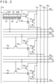
- FIG. 3 is an equivalent circuit diagram of the imaging element of Embodiment 1.
- FIG. 4 is a schematic layout drawing of a first electrode and a charge storage electrode and transistors constituting a control section that constitute the imaging element of Embodiment 1.
- FIG. 5 is a diagram schematically depicting a state of potential at each part at the time of an operation of the imaging element of Embodiment 1.
- FIGS. 6 A, 6 B, and 6 C are equivalent circuit diagrams of imaging elements of Embodiments 1, 4, and 6 for explaining each part of FIG. 5 (Embodiment 1), FIGS. 20 and 21 (Embodiment 4), and FIGS. 32 and 33 (Embodiment 6).
- FIG. 7 is a schematic layout drawing of the first electrode and the charge storage electrode constituting the imaging element of Embodiment 1.
- FIG. 8 is a schematic perspective view of the first electrode, the charge storage electrode, a second electrode, and a contact hole section constituting the imaging element of Embodiment 1.
- FIG. 9 is an equivalent circuit diagram of a modification of the imaging element of Embodiment 1.
- FIG. 10 is a schematic layout drawing of a first electrode and a charge storage electrode and transistors constituting a control section that constitute the modification of the imaging element of Embodiment 1 depicted in FIG. 9 .
- FIG. 11 is a schematic partial sectional view of an imaging element of Embodiment 2.
- FIG. 12 is a schematic partial sectional view of an imaging element of Embodiment 3.
- FIG. 13 is a schematic partial sectional view of a modification of the imaging element of Embodiment 3.
- FIG. 14 is a schematic partial sectional view of another modification of the imaging element of Embodiment 3.
- FIG. 15 is a schematic partial sectional view of a further modification of the imaging element of Embodiment 3.
- FIG. 16 is a schematic partial sectional view of a part of an imaging element of Embodiment 4.
- FIG. 17 is an equivalent circuit diagram of the imaging element of Embodiment 4.
- FIG. 18 is an equivalent circuit diagram of the imaging element of Embodiment 4.
- FIG. 19 is a schematic layout drawing of a first electrode, a transfer control electrode, and a charge storage electrode and transistors constituting a control section that constitute the imaging element of Embodiment 4.
- FIG. 20 is a diagram schematically depicting a state of potential at each part at the time of an operation of the imaging element of Embodiment 4.
- FIG. 21 is a diagram schematically depicting a state of potential at each part at the time of another operation of the imaging element of Embodiment 4.
- FIG. 22 is a schematic layout drawing of the first electrode, the transfer control electrode, and the charge storage electrode constituting the imaging element of Embodiment 4.
- FIG. 23 is a schematic perspective view of the first electrode, the transfer control electrode, the charge storage electrode, a second electrode, and a contact hole section that constitute the imaging element of Embodiment 4.
- FIG. 24 is a schematic layout drawing of the first electrode, the transfer control electrode, and the charge storage electrode, and transistors constituting a control section that constitute a modification of the imaging element of Embodiment 4.
- FIG. 25 is a schematic partial sectional view of a part of an imaging element of Embodiment 5.
- FIG. 26 is a schematic layout drawing of a first electrode, a charge storage electrode, and a charge discharge electrode constituting the imaging element of Embodiment 5.
- FIG. 27 is a schematic perspective view of the first electrode, the charge storage electrode, the charge discharge electrode, a second electrode, and a contact hole section constituting the imaging element of Embodiment 5.
- FIG. 28 is a schematic partial sectional view of an imaging element of Embodiment 6.
- FIG. 29 is an equivalent circuit diagram of the imaging element of Embodiment 6.
- FIG. 30 is an equivalent circuit diagram of the imaging element of Embodiment 6.
- FIG. 31 is a schematic layout drawing of a first electrode and a charge storage electrode and transistors constituting a control section that constitute the imaging element of Embodiment 6.
- FIG. 32 is a diagram schematically depicting a state of potential at each part at the time of an operation of the imaging element of Embodiment 6.
- FIG. 33 is a diagram schematically depicting a state of potential at each part at the time of another operation (transfer) of the imaging element of Embodiment 6.
- FIG. 34 is a schematic layout drawing of the first electrode and the charge storage electrode constituting the imaging element of Embodiment 6.
- FIG. 35 is a schematic perspective view of the first electrode, the charge storage electrode, a second electrode, and a contact hole section constituting the imaging element of Embodiment 6.
- FIG. 36 is a schematic layout drawing of a first electrode and a charge storage electrode constituting a modification of the imaging element of Embodiment 6.
- FIG. 37 is a schematic partial sectional view of an imaging element of Embodiment 7.
- FIG. 38 is a schematic partial sectional view, in an enlarged form, of a part in which a charge storage electrode, a photoelectric conversion layer, and a second electrode are stacked in the imaging element of Embodiment 7.
- FIG. 39 is a schematic layout drawing of a first electrode and a charge storage electrode and transistors constituting a control section that constitute a modification of the imaging element of Embodiment 7.
- FIG. 40 is a schematic partial sectional view, in an enlarged form, of a part in which a charge storage electrode, a photoelectric conversion layer, and a second electrode are stacked in an imaging element of Embodiment 8.
- FIG. 41 is a schematic partial sectional view of an imaging element of Embodiment 9.
- FIG. 42 is a schematic partial sectional view of an imaging element of Embodiment 10 and Embodiment 11.
- FIGS. 43 A and 43 B are schematic plan views of a charge storage electrode segment in Embodiment 11.
- FIGS. 44 A and 44 B are schematic plan views of the charge storage electrode segment in Embodiment 11.
- FIG. 45 is a schematic layout drawing of a first electrode and the charge storage electrode and transistors constituting a control section that constitute the imaging element of Embodiment 11.
- FIG. 46 is a schematic layout drawing of a first electrode and a charge storage electrode constituting a modification of the imaging element of Embodiment 11.
- FIG. 47 is a schematic partial sectional view of an imaging element of Embodiment 12 and Embodiment 11.
- FIGS. 48 A and 48 B are schematic plan views of a charge storage electrode segment in Embodiment 12.
- FIG. 49 is a schematic plan view of a first electrode and a charge storage electrode segment in a solid-state imaging apparatus of Embodiment 13.
- FIG. 50 is a schematic plan view of a first electrode and a charge storage electrode segment in a first modification of the solid-state imaging apparatus of Embodiment 13.
- FIG. 51 is a schematic plan view of a first electrode and a charge storage electrode segment in a second modification of the solid-state imaging apparatus of Embodiment 13.
- FIG. 52 is a schematic plan view of a first electrode and a charge storage electrode segment in a third modification of the solid-state imaging apparatus of Embodiment 13.
- FIG. 53 is a schematic plan view of a first electrode and a charge storage electrode segment in a fourth modification of the solid-state imaging apparatus of Embodiment 13.
- FIG. 54 is a schematic plan view of a first electrode and a charge storage electrode segment in a fifth modification of the solid-state imaging apparatus of Embodiment 13.
- FIG. 55 is a schematic plan view of a first electrode and a charge storage electrode segment in a sixth modification of the solid-state imaging apparatus of Embodiment 13.
- FIG. 56 is a schematic plan view of a first electrode and a charge storage electrode segment in a seventh modification of the solid-state imaging apparatus of Embodiment 13.
- FIG. 57 is a schematic plan view of a first electrode and a charge storage electrode segment in an eighth modification of the solid-state imaging apparatus of Embodiment 13.
- FIG. 58 is a schematic plan view of a first electrode and a charge storage electrode segment in a ninth modification of the solid-state imaging apparatus of Embodiment 13.
- FIGS. 59 A, 59 B, and 59 C are flowcharts depicting a reading driving example in an imaging element block of Embodiment 13.
- FIG. 60 is a schematic plan view of a first electrode and a charge storage electrode segment in a solid-state imaging apparatus of Embodiment 14.
- FIG. 61 is a schematic plan view of a first electrode and a charge storage electrode segment in a modification of the solid-state imaging apparatus of Embodiment 14.
- FIG. 62 is a schematic plan view of a first electrode and a charge storage electrode segment in a modification of the solid-state imaging apparatus of Embodiment 14.
- FIG. 63 is a schematic plan view of a first electrode and a charge storage electrode segment in a modification of the solid-state imaging apparatus of Embodiment 14.
- FIG. 64 is a schematic partial sectional view of another modification of the imaging element of Embodiment 1.
- FIG. 65 is a schematic partial sectional view of a further modification of the imaging element of Embodiment 1.
- FIGS. 66 A, 66 B, and 66 C are schematic partial sectional views, in an enlarged form, of a part of a first electrode and the like in a further modification of the imaging element of Embodiment 1.
- FIG. 67 is a schematic partial sectional view, in an enlarged form, of a part of a charge discharge electrode and the like in another modification of the imaging element of Embodiment 5.
- FIG. 68 is a schematic partial sectional view of a further modification of the imaging element of Embodiment 1.
- FIG. 69 is a schematic partial sectional view of a further modification of the imaging element of Embodiment 1.
- FIG. 70 is a schematic partial sectional view of a further modification of the imaging element of Embodiment 1.
- FIG. 71 is a schematic partial sectional view of a further modification of the imaging element of Embodiment 4.
- FIG. 72 is a schematic partial sectional view of a further modification of the imaging element of Embodiment 1.
- FIG. 73 is a schematic partial sectional view of a further modification of the imaging element of Embodiment 4.
- FIG. 74 is a schematic partial sectional view, in an enlarged form, of a part in which a charge storage electrode, a photoelectric conversion layer, and a second electrode are stacked in a modification of the imaging element of Embodiment 7.
- FIG. 75 is a schematic partial sectional view, in an enlarged form, of a part in which a charge storage electrode, a photoelectric conversion layer, and a second electrode are stacked in a modification of the imaging element of Embodiment 8.
- FIG. 76 is a graph of the relation between V gs and I d in a TFT in which a channel forming region includes In a Ga b Sn c Zn d O e or the like.
- FIGS. 77 A and 77 B are graphs depicting evaluation results of dark current characteristic and external quantum efficiency for an evaluation sample and a comparative sample, respectively, in Embodiment 1.
- FIG. 78 is a conceptual diagram of a solid-state imaging apparatus of Embodiment 1.
- FIG. 79 is a conceptual diagram of an example in which a solid-state imaging apparatus including an imaging element of the present disclosure and the like is used in an electronic apparatus (camera).
- FIG. 80 is a block diagram depicting an example of schematic configuration of a vehicle control system.
- FIG. 81 is a diagram of assistance in explaining an example of installation positions of an outside-vehicle information detecting section and an imaging section.
- FIG. 82 is a view depicting an example of a schematic configuration of an endoscopic surgery system.
- FIG. 83 is a block diagram depicting an example of a functional configuration of a camera head and a camera control unit (CCU).
- CCU camera control unit
- FIG. 84 is a conceptual diagram of a conventional stacked-type imaging element (stacked-type solid-state imaging apparatus).
- imaging element of present disclosure stacked-type imaging element of present disclosure, and solid-state imaging apparatus according to first and second modes of present disclosure
- Embodiment 1 Imaging element of present disclosure, stacked-type imaging element of present disclosure, and solid-state imaging apparatus according to second mode of present disclosure
- Embodiment 2 (Modification of Embodiment 1)
- Embodiment 3 Modifications of Embodiments 1 and 2, solid-state imaging apparatus according to first mode of present disclosure
- Embodiment 4 (Modifications of Embodiments 1 to 3, imaging element including transfer control electrode)
- Embodiment 5 (Modifications of Embodiments 1 to 4, imaging element including charge discharge electrode)
- Embodiment 6 (Modifications of Embodiments 1 to 5, imaging element including plurality of charge storage electrode segments)
- Embodiment 7 (Imaging elements of first and sixth configurations)
- Embodiment 8 (Imaging elements of second and sixth configurations of present disclosure)
- Embodiment 9 (Imaging element of third configuration)
- Embodiment 10 (Imaging element of fourth configuration)
- Embodiment 11 (Imaging element of fifth configuration)
- Embodiment 12 (Imaging element of sixth configuration)
- Embodiment 13 Solid-state imaging apparatuses of first and second configurations
- Embodiment 14 Modification of Embodiment 13
- an imaging element of the present disclosure that constitutes a stacked-type imaging element of the present disclosure, and an imaging element of the present disclosure that constitutes solid-state imaging apparatuses of first and second modes of the present disclosure (these imaging elements may hereinafter be referred to generically as “imaging element or the like of the present disclosure”)
- imaging element or the like of the present disclosure when an inorganic oxide semiconductor material layer is represented by In a Ga b Sn c Zn d O e , 1.8 ⁇ ( b+c )/ a ⁇ 2.3 and 2.3 ⁇ d/a ⁇ 2.6 can be satisfied. Further, b>0 can be satisfied. Note that while an example of the ratio of b/c can include 1/9 to 9/1, a ratio of 1/1 is most preferable.
- the inorganic oxide semiconductor material layer may include other metal atoms in addition to indium (In) atoms, gallium (Ga) atoms, tin (Sn) atoms, and zinc (Zn) atoms. Besides, it is preferable that 3.3 ⁇ e/a ⁇ 8.5 is satisfied.
- a photoelectric conversion section can further include an insulating layer, and a charge storage electrode that is disposed spaced from a first electrode and is disposed to face an inorganic oxide semiconductor material layer, with the insulating layer interposed therebetween.
- a LUMO value E 1 of the material constituting a part of the photoelectric conversion layer located in the vicinity of the inorganic oxide semiconductor material layer and a LUMO value E 2 of the material constituting the inorganic oxide semiconductor material layer can satisfy preferably E 2 ⁇ E 1 ⁇ 0.1 eV, and more preferably E 2 ⁇ E 1 >0.1 eV.
- the part of the photoelectric conversion layer located in the vicinity of the inorganic oxide semiconductor material layer refers to the part of the photoelectric conversion layer located in a region corresponding to within 10% of the thickness of the photoelectric conversion layer (or a region within 0% to 10% of the thickness of the photoelectric conversion layer) with an interface between the inorganic oxide semiconductor material layer and the photoelectric conversion layer as a reference.
- the LUMO value E 1 of the material constituting the part of the photoelectric conversion layer located in the vicinity of the inorganic oxide semiconductor material layer is an average value of the part of the photoelectric conversion layer located in the vicinity of the inorganic oxide semiconductor material layer
- the LUMO value E 2 of the material constituting the inorganic oxide semiconductor material layer is an average value of the inorganic oxide semiconductor material layer.
- the mobility of the material constituting the inorganic oxide semiconductor material layer can be equal to or more than 10 cm 2 /V ⁇ s.
- the inorganic oxide semiconductor material layer can be amorphous (for example, be amorphous and not locally having a crystalline structure). Whether or not the inorganic oxide semiconductor material layer is amorphous can be determined based on X-ray diffraction analysis.
- the thickness of the inorganic oxide semiconductor material layer can be 1 ⁇ 10 ⁇ 8 to 1.5 ⁇ 10 ⁇ 7 m, preferably 2 ⁇ 10 ⁇ 8 to 1.0 ⁇ 10 ⁇ 7 m, and more preferably 3 ⁇ 10 ⁇ 8 to 1.0 ⁇ 10 ⁇ 7 m.
- the surface roughness Ra of the inorganic oxide semiconductor material layer at the interface between the photoelectric conversion layer and the inorganic oxide semiconductor material layer can be equal to or less than 1.5 nm, and the value of root mean square roughness Rq of the inorganic oxide semiconductor material layer can be equal to or less than 2.5 nm.
- the surface roughnesses Ra and Rq are based on the prescription of JIS B0601:2013. Such smoothness of the inorganic oxide semiconductor material layer at the interface of the photoelectric conversion layer and the inorganic oxide semiconductor material layer makes it possible to restrain surface scattering reflection at the inorganic oxide semiconductor material layer, and to enhance light current characteristic in photoelectric conversion.
- the surface roughness Ra of the charge storage electrode can be equal to or less than 1.5 nm, and the value of root mean square roughness Rq of the charge storage electrode can be equal to or less than 2.5 nm.
- the carrier density of the inorganic oxide semiconductor material layer is preferably less than 1 ⁇ 10 16 /cm 3 .
- charges generated by photoelectric conversion in a second photoelectric conversion section 341 A and a third photoelectric conversion section 343 A are once stored in the second photoelectric conversion section 341 A and the third photoelectric conversion section 343 A, and are thereafter transferred to a second floating diffusion layer FD 2 and a third floating diffusion layer FD 3 . Therefore, the second photoelectric conversion section 341 A and the third photoelectric conversion section 343 A can be completely depleted.
- charges generated by photoelectric conversion in a first photoelectric conversion section 310 A are stored directly in a first floating diffusion layer FD 1 . Therefore, it is difficult to completely deplete the first photoelectric conversion section 310 A. As a result, kTC noise may be enlarged, and random noise may be worsened, leading to a lowering in picked-up image quality.
- the charge storage electrode is provided which is disposed spaced from the first electrode and is disposed to face the inorganic oxide semiconductor material layer, with the insulating layer interposed therebetween, so that it is ensured that when the photoelectric conversion section is irradiated with light and photoelectric conversion occurs in the photoelectric conversion section, charges can be stored in the inorganic oxide semiconductor material layer (in some cases, in the inorganic oxide semiconductor material layer and the photoelectric conversion layer). Therefore, when exposure is started, the charge storage section can be completely depleted, and the charges can be eliminated.
- the inorganic oxide semiconductor material layer or the inorganic oxide semiconductor material layer and the photoelectric conversion layer, may be referred to generically as “the inorganic oxide semiconductor material layer and the like.”
- the inorganic oxide semiconductor material layer may have a monolayer configuration or a multilayer configuration.
- the material constituting the inorganic oxide semiconductor material layer located on an upper side of the charge storage electrode and the material constituting the inorganic oxide semiconductor material layer located on an upper side of the first electrode may be different from each other.
- the inorganic oxide semiconductor material layer may be formed, for example, based on a sputtering method.
- the sputtering method include a sputtering method in which a parallel flat plate sputtering apparatus or a DC magnetron sputtering apparatus is used as a sputtering apparatus, an argon (Ar) gas is used as a process gas, and an In a Ga b Sn c Zn d O e sintered body is used as a target.
- the energy level of the inorganic oxide semiconductor material layer can be controlled based on the oxygen content, and the energy level can be made deeper as the oxygen content is lower than the stoichiometric oxygen content, namely, as oxygen deficiency is larger.
- the imaging element or the like of the present disclosure which includes the above-described preferred modes and which includes the charge storage electrode may hereinafter be referred to as “the imaging element or the like including the charge storage electrode of the present disclosure,” for convenience' sake.
- the light transmittance of the inorganic oxide semiconductor material layer with respect to light of a wavelength of 400 to 660 nm is preferably equal to or more than 65%.
- the light transmittance of the charge storage electrode with respect to light of a wavelength of 400 to 660 nm is also preferably equal to or more than 65%.
- the sheet resistance of the charge storage electrode is preferably 3 ⁇ 10 to 1 ⁇ 10 3 ⁇ / ⁇ .
- the imaging element or the like can further include a semiconductor substrate, and
- the photoelectric conversion section can be disposed on an upper side of the semiconductor substrate.
- the first electrode, the charge storage electrode, and the second electrode are connected to a driving circuit which will be described later.
- the second electrode located on the light incidence side may be common to a plurality of imaging elements.
- the second electrode may be a so-called solid electrode.
- the photoelectric conversion layer may be common to a plurality of imaging elements.
- one photoelectric conversion layer may be formed for the plurality of imaging elements, or may be provided on the basis of each imaging element.
- the inorganic oxide semiconductor material layer is preferably provided on the basis of each imaging element, but, in some cases, may be common to a plurality of imaging elements.
- a charge movement control electrode which will be described later may be provided between an imaging element and another imaging element, so that one inorganic oxide semiconductor material layer may be formed for a plurality of imaging elements.
- the first electrode can extend in an opening provided in the insulating layer, and can be connected to the inorganic oxide semiconductor material layer.
- the inorganic oxide semiconductor material layer can extend in the opening provided in the insulating layer, and can be connected to the first electrode.
- an edge portion of a top surface of the first electrode can be covered with the insulating layer
- the first electrode can be exposed at a bottom surface of the opening
- a side surface of the opening can have such an inclination as to broaden from the first surface toward the second surface, and, further, the side surface of the opening having the inclination such as to broaden from the first surface toward the second surface can be located on the charge storage electrode side.
- the imaging element or the like can further include a control section which is provided on the semiconductor substrate and which has a driving circuit,
- the first electrode and the charge storage electrode can be connected to the driving circuit, in a charge storage period, from the driving circuit, a potential V 11 can be impressed on the first electrode, a potential V 12 can be impressed on the charge storage electrode, and charges can be stored in the inorganic oxide semiconductor material layer (or in the inorganic oxide semiconductor material layer and the photoelectric conversion layer), and
- a potential V 21 can be impressed on the first electrode
- a potential V 22 can be impressed on the charge storage electrode
- the charges stored in the inorganic oxide semiconductor material layer (or in the inorganic oxide semiconductor material layer and the photoelectric conversion layer) can be read out to the control section via the first electrode. It is to be noted, however, that the potential of the first electrode is higher than the potential of the second electrode, and
- V 12 ⁇ V 11 , and V 22 ⁇ V 21 are satisfied.
- the imaging element or the like including the charge storage electrode of the present disclosure can further include, between the first electrode and the charge storage electrode, a transfer control electrode (charge transfer electrode) which is disposed spaced from the first electrode and the charge storage electrode and which is disposed to face the inorganic oxide semiconductor material layer, with the insulating layer interposed therebetween.
- a transfer control electrode charge transfer electrode
- the imaging element or the like including the charge storage electrode of the present disclosure in such a mode will be referred to as “the imaging element or the like including the transfer control electrode of the present disclosure” for convenience' sake.
- the imaging element or the like can further include a control section which is provided on the semiconductor substrate and which has the driving circuit,
- the first electrode, the charge storage electrode, and the transfer control electrode can be connected to the driving circuit
- a potential V 11 can be impressed on the first electrode
- a potential V 12 can be impressed on the charge storage electrode
- a potential V 13 can be impressed on the transfer control electrode
- charges can be stored in the inorganic oxide semiconductor material layer (or in the inorganic oxide semiconductor material layer and the photoelectric conversion layer)
- a potential V 21 can be impressed on the first electrode
- a potential V 12 can be impressed on the charge storage electrode
- a potential V 13 can be impressed on the transfer control electrode
- the charges stored in the inorganic oxide semiconductor material layer (or in the inorganic oxide semiconductor material layer and the photoelectric conversion layer) can be read out to the control section via the first electrode.
- the potential of the first electrode is higher than the potential of the second electrode
- V 11 >V 13
- V 22 ⁇ V 23 ⁇ V 21 are satisfied.
- the imaging element or the like including the charge storage electrode of the present disclosure including the above-described various preferred modes may further include a charge discharge electrode which is connected to the inorganic oxide semiconductor material layer and which is disposed spaced from the first electrode and the charge storage electrode.
- the imaging element or the like including the charge storage electrode of the present disclosure in such a mode will be referred to as “the imaging element or the like including the charge discharge electrode of the present disclosure” for convenience' sake.
- the charge discharge electrode can be disposed such as to surround the first electrode and the charge storage electrode (in other words, in a picture frame form).
- the charge discharge electrode can be common to a plurality of imaging elements. In this case,
- the inorganic oxide semiconductor material layer can extend in a second opening provided in the insulating layer and can be connected to the charge discharge electrode
- an edge portion of a top surface of the charge discharge electrode can be covered with the insulating layer
- the charge discharge electrode can be exposed at a bottom surface of the second opening
- a side surface of the second opening can have an inclination such as to broaden from the third surface toward the second surface.
- the imaging element or the like can further include the control section which is provided on the semiconductor substrate and which has the driving circuit,
- the first electrode, the charge storage electrode, and the charge discharge electrode can be connected to the driving circuit
- the potential V 11 can be impressed on the first electrode
- the potential V 12 can be impressed on the charge storage electrode
- a potential V 14 can be impressed on the charge discharge electrode
- charges can be stored in the inorganic oxide semiconductor material layer (or in the inorganic oxide semiconductor material layer and the photoelectric conversion layer)
- the potential V 21 can be impressed on the first electrode, the potential V 21 can be impressed on the charge storage electrode, a potential V 24 can be impressed on the charge discharge electrode, and the charges stored in the inorganic oxide semiconductor material layer (or in the inorganic oxide semiconductor material layer and the photoelectric conversion layer) can be read out to the control section via the first electrode.
- the potential of the first electrode is higher than the potential of the second electrode, and
- the charge storage electrode can include a plurality of charge storage electrode segments.
- the imaging element or the like including the charge storage electrode of the present disclosure in such a mode will be referred to as “the imaging element or the like including the plurality of charge storage electrode segments of the present disclosure” for convenience' sake.
- the number of the charge storage electrode segments need only be equal to or more than two.
- the imaging element or the like including the plurality of charge storage electrode segments of the present disclosure in the case where different potentials are impressed respectively on N charge storage electrode segments,
- the potential impressed on the charge storage electrode segment located at a nearest place to the first electrode (a first photoelectric conversion section segment) in the charge transfer period can be higher than the potential impressed on the charge storage electrode segment located at a farthest place from the first electrode (an N-th photoelectric conversion section segment), and
- the potential impressed on the charge storage electrode segment located at the nearest place to the first electrode (the first photoelectric conversion section segment) in the charge transfer period can be lower than the potential impressed on the charge storage electrode segment located at the farthest place from the first electrode (the N-th photoelectric conversion section segment).
- the semiconductor substrate can be provided with at least a floating diffusion layer and an amplification transistor that constitute the control section, and
- the first electrode can be connected to the floating diffusion layer and a gate section of the amplification transistor. In this case, further,
- the semiconductor substrate can be provided further with a reset transistor and a select transistor that constitute the control section,
- the floating diffusion layer can be connected to a source/drain region on one side of the reset transistor, and
- a source/drain region on one side of the amplification transistor can be connected to a source/drain region on one side of the select transistor, and a source/drain region on the other side of the select transistor can be connected to a signal line.
- the size of the charge storage electrode can be larger than the size of the first electrode. Let the area of the charge storage electrode be S 1 ′ and let the area of the first electrode be S 1 , then it is preferable that 4 ⁇ S 1 ′/S 1 is satisfied, though this is not limitative.
- modifications of the imaging element or the like of the present disclosure including the above-described various preferred modes can include imaging elements of first to sixth configurations described below.
- imaging elements of the first to sixth configurations of the imaging element or the like of the present disclosure including the above-described various preferred modes can include imaging elements of first to sixth configurations described below.
- the photoelectric conversion section includes N (where N ⁇ 2) photoelectric conversion section segments,
- the inorganic oxide semiconductor material layer and the photoelectric conversion layer include N photoelectric conversion layer segments,
- the insulating layer includes N insulating layer segments
- the charge storage electrode includes N charge storage electrode segments
- the charge storage electrode includes N charge storage electrode segments disposed spaced from one another,
- the photoelectric conversion section segment with a larger n value is located spaced more from the first electrode.
- the photoelectric conversion layer segment refers to a segment in which the photoelectric conversion layer and the inorganic oxide semiconductor material layer are stacked.
- the thickness of the insulating layer segment varies gradually over a range from the first photoelectric conversion section segment to the N-th photoelectric conversion section segment.
- the thickness of the photoelectric conversion layer segment varies gradually over a range from the first photoelectric conversion section segment to the N-th photoelectric conversion section segment.
- the thickness of the photoelectric conversion layer segment may be varied, with the thickness of the part of the photoelectric conversion layer being varied and with the thickness of the part of the inorganic oxide semiconductor material layer being constant, the thickness of the photoelectric conversion layer segment may be varied, with the thickness of the part of the photoelectric conversion layer being constant and with the thickness of the part of the inorganic oxide semiconductor material layer being varied, or the thickness of the photoelectric conversion layer segment may be varied, with the thickness of the part of the photoelectric conversion layer being varied and with the thickness of the part of the inorganic oxide semiconductor material layer being varied. Further, in the imaging element of the third configuration, the material constituting the insulating layer segment differs between adjacent photoelectric conversion section segments.
- the material constituting the charge storage electrode segment differs between adjacent photoelectric conversion section segments.
- the area of the charge storage electrode segment is reduced gradually over a range from the first photoelectric conversion section segment to the N-th photoelectric conversion section segment. The area may be reduced continuously, or may be reduced stepwise.
- the imaging element of the sixth configuration of the imaging element or the like of the present disclosure including the above-described various preferred modes, let the stacking direction of the charge storage electrode, the insulating layer, the inorganic oxide semiconductor material layer, and the photoelectric conversion layer be a Z direction, and let the direction for spacing away from the first electrode be an X direction, then the sectional area of a stacked part of the charge storage electrode, the insulating layer, the inorganic oxide semiconductor material layer, and the photoelectric conversion layer when the stacked part is cut in a YZ virtual plane varies depending on the distance from the first electrode.
- the sectional area may vary continuously, or may vary stepwise.
- the N photoelectric conversion layer segments are provided continuously, the N insulating layer segments are also provided continuously, and the N charge storage electrode segments are also provided continuously.
- the N photoelectric conversion layer segments are provided continuously.
- the N insulating layer segments are provided continuously whereas, in the imaging element of the third configuration, the N insulating layer segments are provided correspondingly to the respective photoelectric conversion section segments.
- the N charge storage electrode segments are provided correspondingly to the respective photoelectric conversion section segments.
- the same potential is impressed on all the charge storage electrode segments.
- different potentials may be impressed on each of the N charge storage electrode segments.
- the thickness of the insulating layer segment is prescribed, or the thickness of the photoelectric conversion layer segment is prescribed, or the materials constituting the insulating layer segments are different, or the materials constituting the charge storage electrode segments are different, or the area of the charge storage electrode segment is prescribed, or the sectional area of the stacked part is prescribed, and, therefore, a kind of charge transfer gradient is formed, and the charges generated by photoelectric conversion can be transferred to the first electrode more easily and securely. As a result, generation of after-images and generation of leaving untransferred charges can be prevented.
- the photoelectric conversion section segment with a larger n value is located spaced more from the first electrode; in this case, whether or not a segment is located spaced from the first electrode is decided with the X direction as a reference.
- the direction for spacing away from the first electrode is set as the X direction, and “the X direction” is defined as follows.
- a pixel region in which a plurality of imaging elements or stacked-type imaging elements is arranged includes a plurality of pixels arranged in a two-dimensional array, or arranged regularly in the X direction and the Y direction.
- the direction in which a rectangle's side the nearest to the first electrode extends is made to be the Y direction, and the direction orthogonal to the Y direction is made to be the X direction.
- the general direction in which a line segment or a curve the nearest to the first electrode is included is made to be the Y direction, and the direction orthogonal to the Y direction is made to be the X direction.
- the thickness of the insulating layer segment varies gradually over a range from the first photoelectric conversion section segment to the N-th photoelectric conversion section segment; in this case, the thickness of the insulating layer segment preferably increases gradually, and, as a result of this, a kind of charge transfer gradient is formed.
- the n-th photoelectric conversion section segment can store more charges than the (n+1)th photoelectric conversion section segment, and a strong electric field is applied, so that a flow of charges from the first photoelectric conversion section segment to the first electrode can be prevented assuredly.
- the thickness of the photoelectric conversion layer segment varies gradually over a range from the first photoelectric conversion section segment to the N-th photoelectric conversion section segment; in this case, the thickness of the photoelectric conversion layer segment preferably increases gradually, and, as a result of this, a kind of charge transfer gradient is formed.
- a state of V 12 ⁇ V 11 is established in the charge storage period, a stronger electric field is impressed on the n-th photoelectric conversion section segment than on the (n+1)th photoelectric conversion section segment, so that a flow of charges from the first photoelectric conversion section segment to the first electrode can be prevented securely.
- the material constituting the insulating layer segment differs between adjacent photoelectric conversion section segments, so that a kind of charge transfer gradient is formed.
- the material constituting the charge storage electrode segment differs between adjacent photoelectric conversion section segments, and, as a result of this, a kind of charge transfer gradient is formed.
- the value of work function of the material constituting the insulating layer segment is enlarged gradually over a range from the first photoelectric conversion section segment to the N-th photoelectric conversion section segment.
- the area of the charge storage electrode segment is reduced gradually over a range from the first photoelectric conversion section segment to the N-th photoelectric conversion section segment, and, as a result of this, a kind of charge transfer gradient is formed.
- a state of V 12 ⁇ V 11 is established in the charge storage period, therefore, more charge can be stored in the n-th photoelectric conversion section segment than in the (n+1)th photoelectric conversion section segment.
- a state of V 22 ⁇ V 21 is established in the charge transfer period, a flow of charges from the first photoelectric conversion section segment to the first electrode, and a flow of charges from the (n+1)th photoelectric conversion section segment to the n-th photoelectric conversion section segment can be secured assuredly.
- the sectional area of the stacked part varies depending on the distance from the first electrode, and, as a result of this, a kind of charge transfer gradient is formed.
- a configuration is adopted in which the thickness of the section of the stacked part is constant and the width of the section of the stacked part is narrower in going away from the first electrode, it is ensured, like described in the imaging element of the fifth configuration, that when a state of V 12 ⁇ V 11 is established in the charge storage period, more charges can be stored in a region near to the first electrode than in a region far from the first electrode.
- a modification of the solid-state imaging apparatuses of the first and second modes of the present disclosure is a solid-state imaging apparatus including
- the plurality of imaging elements constitutes an imaging element block
- a first electrode is shared by the plurality of imaging elements constituting the imaging element block.
- the solid-state imaging apparatus of such a configuration will be referred to as “the solid-state imaging apparatus of the first configuration” for convenience' sake.
- a modification of the solid-state imaging apparatuses of the first and second modes of the present disclosure may be a solid-state imaging apparatus including
- the plurality of imaging elements or stacked-type imaging elements constitutes an imaging element block
- a first electrode is shared by the plurality of imaging elements or stacked-type imaging elements constituting the imaging element block.
- the solid-state imaging apparatus of such a configuration will be referred to as “the solid-state imaging apparatus of the second configuration” for convenience' sake.
- the first electrode is thus shared by the plurality of imaging elements constituting the imaging element block, the configuration and structure of a pixel region in which a plurality of the imaging elements is arranged can be simplified and made finer.
- one floating diffusion layer is provided for a plurality of imaging elements (one imaging element block).
- the plurality of imaging elements provided for one floating diffusion layer may include a plurality of the imaging elements of a first type described later, or may include at least one imaging element of the first type and one or more imaging elements of a second type described later.
- the plurality of imaging elements can share one floating diffusion layer.
- the plurality of imaging elements is operated in conjunction with one another, and they are connected as an imaging element block to the driving circuit which will be described later. In other words, the plurality of imaging elements constituting the imaging element block is connected to one driving circuit.
- the control of the charge storage electrode is conducted on the basis of each imaging element.
- the plurality of imaging elements can share one contact hole section.
- the layout relation between the first electrode shared by the plurality of imaging elements and the charge storage electrode for each imaging element may be one in which the first electrode is disposed adjacently to the charge storage electrode of each imaging element.
- the first electrode may be disposed adjacently to the charge storage electrodes of some of the plurality of imaging elements but may not be disposed adjacently to the charge storage electrodes of the remaining ones of the plurality of imaging elements; in this case, the movement of charges from the remaining ones of the plurality of imaging elements to the first electrode is a movement via some of the plurality of imaging elements.
- the distance between a charge storage electrode constituting the imaging element and another charge storage electrode constituting the imaging element is longer than the distance between the first electrode and the charge storage electrode in the imaging element adjacent to the first electrode (this distance will be referred to as “distance B” for convenience' sake), for ensuring the movement of charges from each imaging element to the first electrode.
- distance A the distance between a charge storage electrode constituting the imaging element and another charge storage electrode constituting the imaging element
- distance B for convenience' sake
- light can be incident from the second electrode side, and a light shielding layer may be formed on the light incidence side near the second electrode.
- a light shielding layer can be formed on the light incidence side near the second electrode and on an upper side of the first electrode (in some cases, on an upper side of the first electrode and the transfer control electrode), or an on-chip microlens can be provided on an upper side of the charge storage electrode and the second electrode, and the light incident on the on-chip microlens can be concentrated onto the charge storage electrode.
- the light shielding layer may be disposed above a light incidence side surface of the second electrode, or may be disposed on the light incidence side surface of the second electrode.
- the second electrode may be formed with the light shielding layer.
- the material constituting the light shielding layer include chromium (Cr), copper (Cu), aluminum (Al), tungsten (W), and non-light-transmitting resins (for example, polyimide resin).
- the imaging elements of the present disclosure include an imaging element having sensitivity to blue light (referred to as “the blue light imaging element of the first type” for convenience' sake) including a photoelectric conversion layer or a photoelectric conversion section that absorbs blue light (light of 425 to 495 nm) (referred to as “the blue light photoelectric conversion layer of the first type” or “the blue light photoelectric conversion section of the first type” for convenience' sake), an imaging element having sensitivity to green light (referred to as “the green light imaging element of the first type” for convenience' sake) including a photoelectric conversion layer or a photoelectric conversion section that absorbs green light (light of 495 to 570 nm) (referred to as “the green light photoelectric conversion layer of the first type” or “the green light photoelectric conversion section of the first type”), and an imaging element having sensitivity to red light (referred to as “the red light imaging element of the first type” for convenience' sake) including a photoelectric conversion layer or a photoelectric conversion section that absorbs red light (light of 620 to
- the imaging element having sensitivity to blue light is referred to as “the blue light imaging element of the second type” for convenience' sake
- the imaging element having sensitivity to green light is referred to as “the green light imaging element of the second type” for convenience' sake
- the imaging element having sensitivity to red light is referred to as “the red light imaging element of the second type” for convenience' sake.
- the photoelectric conversion layer or the photoelectric conversion section that constitutes the blue light imaging element of the second type is referred to as “the blue light photoelectric conversion layer of the second type” or “the blue light photoelectric conversion section of the second type” for convenience' sake
- the photoelectric conversion layer or the photoelectric conversion section that constitutes the green light imaging element of the second type is referred to as “the green light photoelectric conversion layer of the second type” or “the green light photoelectric conversion section of the second type” for convenience' sake
- the photoelectric conversion layer or the photoelectric conversion section that constitutes the red light imaging element of the second type is referred to as “the red light photoelectric conversion layer of the second type” or “the red light photoelectric conversion section of the second type” for convenience' sake.
- stacked-type imaging element including the charge storage electrode
- [A] a configuration or structure in which the blue light photoelectric conversion section of the first type, the green light photoelectric conversion section of the first type, and the red light photoelectric conversion section of the first type are stacked in the vertical direction, and
- [B] a configuration or structure in which the blue light photoelectric conversion section of the first type and the green light photoelectric conversion section of the first type are stacked in the vertical direction
- the red light photoelectric conversion section of the second type is disposed on a lower side of these two photoelectric conversion sections of the first type
- [C] a configuration or structure in which the blue light photoelectric conversion section of the second type and the red light photoelectric conversion section of the second type are disposed on a lower side of the green light photoelectric conversion section of the first type, and
- [D] a configuration or structure in which the green light photoelectric conversion section of the second type and the red light photoelectric conversion section of the second type are disposed on a lower side of the blue light photoelectric conversion section of the first type, and
- the disposing order of the photoelectric conversion sections of these imaging elements in the vertical direction is preferably the blue light photoelectric conversion section, the green light photoelectric conversion section, and the red light photoelectric conversion section from the light incidence direction, or the green light photoelectric conversion section, the blue light photoelectric conversion section, and the red light photoelectric conversion section from the light incidence direction. This is because light of a shorter wavelength is absorbed more efficiently on the incidence surface side. Since the red light is the longest in wavelength of the three color lights, it is preferable to locate the red light photoelectric conversion section at the lowermost layer as viewed from the light incidence surface. By a stacked layer structure of these imaging elements, one pixel is configured.
- a near infrared light photoelectric conversion section (or an infrared light photoelectric conversion section) of the first type may be provided.
- a photoelectric conversion layer of the infrared light photoelectric conversion section of the first type includes, for example, an organic material, is a lowermost layer in the stacked layer structure of the imaging element of the first type, and is disposed above the imaging element of the second type.
- a near infrared light photoelectric conversion section (or an infrared light photoelectric conversion section) of the second type may be provided on a lower side of the photoelectric conversion sections of the first type.
- the first electrode is formed on an interlayer insulating layer provided on the semiconductor substrate.
- the imaging element formed on the semiconductor substrate may be of a back side illumination type or a front side illumination type.
- the photoelectric conversion layer may be in any of the following four modes:
- stacking order may be rearranged (modified) arbitrarily.
- Examples of the p-type organic semiconductor include naphthalene derivatives, anthracene derivatives, phenanthrene derivatives, pyrene derivatives, perylene derivatives, tetracene derivatives, pentacene derivatives, quinacridone derivatives, thiophene derivatives, thienothiophene derivatives, benzothiophene derivatives, benzothienobenzothiophene derivatives, triallylamine derivatives, carbazole derivatives, perylene derivatives, picene derivatives, chrysene derivatives, fluoranthene derivatives, phthalocyanine derivatives, subphthalocyanine derivatives, subporphyrazine derivatives, metal complexes having a heterocyclic compound as a ligand, polythiophene derivatives, polybenzothiazole derivatives, polyfluorene derivatives, etc.
- n-type organic semiconductor examples include fullerenes and fullerene derivatives ⁇ e.g., fullerenes (higher fullerenes) such as C60, C70, and C74 fullerenes or the like, endohedral fullerene or the like) or fullerene derivatives (e.g., fullerene fluoride, PCBM fullerene compound, fullerene polymer, etc.)>, organic semiconductors with larger (deeper) HOMO and LUMO than those of p-type organic semiconductors, and transparent inorganic metal oxides.
- fullerenes and fullerene derivatives ⁇ e.g., fullerenes (higher fullerenes) such as C60, C70, and C74 fullerenes or the like, endohedral fullerene or the like) or fullerene derivatives (e.g., fullerene fluoride, PCBM fullerene compound, fullerene polymer
- n-type organic semiconductor include heterocyclic compounds containing a nitrogen atom, an oxygen atom, and a sulfur atom, for example, organic molecules and organometallic complexes having pyridine derivatives, pyrazine derivatives, pyrimidine derivatives, triazine derivatives, quinoline derivatives, quinoxaline derivatives, isoquinoline derivatives, acridine derivatives, phenazine derivatives, phenanthroline derivatives, tetrazole derivatives, pyrazole derivatives, imidazole derivatives, thiazole derivatives, oxazole derivatives, imidazole derivatives, benzimidazole derivatives, benzotriazole derivatives, benzoxazole derivatives, benzoxazole derivatives, carbazole derivatives, benzofuran derivatives, dibenzofuran derivatives, subporphyrazine derivatives, polyphenylene vinylene derivatives, polybenzothiadiazole derivatives, polyfluorene derivative
- Examples of a group or the like included in fullerene derivatives include a halogen atom; a linear, branched, or cyclic alkyl group or phenyl group; a group having a linear or condensed aromatic compound; a group having a halide; a partial fluoroalkyl group; a perfluoroalkyl group; a silylalkyl group; a silylalkoxy group; an arylsilyl group; an arylsulfanyl group; an alkylsulfanyl group; an arylsulfonyl group; an alkylsulfonyl group; an arylsulfide group; an alkylsulfide group; an amino group; an alkylamino group; an arylamino group; a hydroxy group; an alkoxy group; an acylamino group; an acyloxy group; a carbonyl group; a carboxy group; a carboxamide
- the thickness of the photoelectric conversion layer (may be referred to as “the organic photoelectric conversion layer”) including an organic material may be, without being limited to, 1 ⁇ 10 ⁇ 8 to 5 ⁇ 10 ⁇ 7 m, preferably 2.5 ⁇ 10 ⁇ 8 to 3 ⁇ 10 ⁇ 7 m, more preferably 2.5 ⁇ 10 ⁇ 8 to 2 ⁇ 10 ⁇ 7 m, and still more preferably 1 ⁇ 10 ⁇ 7 to 1.8 ⁇ 10 ⁇ 7 m.
- organic semiconductors are often classified as p-type or n-type, p-type means that holes can be easily transported, and n-type means that electrons can be easily transported, and an organic semiconductor is not limited to the interpretation that it has holes or electrons as majority carriers of thermal excitation as in inorganic semiconductors.
- examples of the material constituting an organic photoelectric conversion layer that photoelectrically converts green light include rhodamine-based coloring matter, melacyanine-based coloring matter, quinacridone derivative, subphthalocyanine-based coloring matter (subphthalocyanine derivative), etc.
- examples of the material constituting an organic photoelectric conversion layer that photoelectrically converts blue light include coumarinic acid coloring matter, tris-8-hydroxyquinolinato aluminum (Alq3), melacyanine-based coloring matter, etc.
- Examples of the material constituting an organic photoelectric conversion layer that photoelectrically converts red light include phthalocyanine-based coloring matter and subphthalocyanine-based coloring matter (subphthalocyanine derivative), etc.
- examples of the inorganic material constituting the photoelectric conversion layer include crystalline silicon, amorphous silicon, microcrystalline silicon, crystalline selenium, amorphous selenium, chalcopyrite compounds such as CIGS (CuInGaSe), CIS (CuInSe 2 ), CuInS 2 , CuAlS 2 , CuAlSe 2 , CuGaS 2 , CuGaSe 2 , AgAlS 2 , AgAlSe 2 , AgInS 2 , AgInSe 2 , group III-V compounds such as GaAs, InP, AlGaAs, InGaP, AlGaInP, InGaAsP, and compound semiconductors such as CdSe, CdS, In 2 Se 3 , In 2 S 3 , Bi 2 Se 3 , Bi 2 S 3 , ZnSe, ZnS, PbSe, PbS, etc.
- quantum dots including these materials may be used in the photoelectric conversion layer.
- a single plate type color solid-state imaging apparatus can be configured.
- the solid-state imaging apparatus including the stacked-type imaging element, unlike the solid-state imaging apparatus including the Bayer-array imaging element (namely, spectroscopy for blue, green, and red is not performed using a color filter), imaging elements having sensitivity to light of plural types of wavelengths are stacked in the light incidence direction in the same pixel to form one pixel, and, therefore, improvement of sensitivity and pixel density per unit volume can be achieved.
- an organic material has a high absorption coefficient
- the film thickness of a photoelectric conversion layer can be thin as compared to a conventional Si-based photoelectric conversion layer, and light leakage from adjacent pixels and restriction on the light incidence angle can be alleviated.
- the conventional Si-based imaging element produces color signals by performing interpolation processing among three-color pixels, false color is generated, but false color can be suppressed in the solid-state imaging apparatus according to the second mode of the present disclosure including the stacked-type imaging element. Since the organic photoelectric conversion layer itself functions also as a color filter layer, color separation can be performed without disposing a color filter layer.
- a color filter layer is used, so that the request for spectral characteristics of blue, green, and red can be alleviated, and mass productivity is high.
- Examples of the arrangement of the imaging elements in the solid-state imaging apparatus according to the first mode of the present disclosure include an interline arrangement, a G stripe-RB checkered array, a G stripe-RB full-checkered array, a checkered complementary color array, a stripe array, a diagonal stripe array, a primary color difference array, a field color difference sequential array, a frame color difference sequential array, an MOS-type array, a modified MOS-type array, a frame interleave array, and a field interleave array in addition to a Bayer array.
- one pixel (or sub-pixel) includes one imaging element.
- the color filter layer examples include filter layers that transmit specific wavelengths of not only red, green, and blue, but also, in some cases, cyan, magenta, yellow, or the like.
- the color filter layers may include not only organic material color filter layers using organic compounds such as pigments and dyes, but also thin films of inorganic materials such as a photonic crystal, a wavelength selecting element based on application of plasmon (a color filter layer having a conductor lattice structure in which a conductor thin film is provided with a lattice shaped hole structure; see, for example, JP 2008-177191A), amorphous silicon, etc.
- the pixel region in which a plurality of imaging elements of the present disclosure is arranged includes a plurality of pixels arranged regularly in a two-dimensional array.
- the pixel region includes an effective pixel region that actually receives light, amplifies a signal charge generated by photoelectric conversion, and reads the amplified signal charge out to a driving circuit, and a black reference pixel region (also called optical black pixel region (OPB)) for outputting optical black to be a reference of black level.
- OPB optical black pixel region
- the black reference pixel region is disposed in the periphery of the effective pixel region.
- irradiation with light is performed, photoelectric conversion is generated in the photoelectric conversion layer, and holes and electrons are subjected to carrier separation.
- An electrode where the holes are taken out is made to be an anode, and an electrode where the electrons are taken out is made to be a cathode.
- the first electrode constitutes the cathode, and the second electrode constitutes the anode.
- the first electrode, the charge storage electrode, the transfer control electrode, the charge discharge electrode, and the second electrode may include a transparent conductive material.
- the first electrode, the charge storage electrode, the transfer control electrode, and the charge discharge electrode may be referred to generically as “the first electrode or the like.”
- the second electrode may include a transparent conductive material and the first electrode or the like may include a metallic material.
- the second electrode located on the light incidence side can include a transparent conductive material
- the first electrode or the like can include Al—Nd (alloy of aluminum and neodymium) or ASC (alloy of aluminum, samarium, and copper).
- An electrode including a transparent conductive material may be referred to as a “transparent electrode.”
- the band gap energy of the transparent conductive material is equal to or more than 2.5 eV, preferably equal to or more than 3.1 eV.
- the transparent conductive material constituting the transparent electrode include conductive metallic oxides, and specific examples thereof include indium oxide, indium tin oxide (ITO including Sn-doped In 2 O 3 , crystalline ITO, and amorphous ITO), indium zinc oxide (IZO) in which indium is added to zinc oxide as a dopant, indium gallium oxide (IGO) in which indium is added to gallium oxide as a dopant, indium gallium zinc oxide (IGZO, In—GaZnO 4 ) in which indium and gallium are added to zinc oxide as a dopant, indium tin zinc oxide (ITZO) in which indium and tin are added to zinc oxide as a dopant, IFO (F-doped In 2 O 3 ), tin oxide (SnO 2 ), ATO (Sb-doped SnO 2 ), FTO (F-doped SnO 2 ), zinc oxide (including ZnO doped with other elements), aluminum zinc oxide
- a transparent electrode having a base layer of gallium oxide, titanium oxide, niobium oxide, nickel oxide, or the like may be mentioned as an example.
- the thickness of the transparent electrode may be 2 ⁇ 10 ⁇ 8 to 2 ⁇ 10 ⁇ 7 m, preferably 3 ⁇ 10 ⁇ 8 to 1 ⁇ 10 ⁇ 7 m.
- the charge discharge electrode also include a transparent conductive material from the viewpoint of simplifying the manufacturing process.
- alkali metals e.g., Li, Na, K, etc.
- alkaline earth metals e.g., Mg, Ca, etc.
- Al aluminum
- Zn zinc
- Sn tin
- Tl
- examples of the material for constituting the cathode include metals such as platinum (Pt), gold (Au), palladium (Pd), chromium (Cr), nickel (Ni), aluminum (Al), silver (Ag), tantalum (Ta), tungsten (W), copper (Cu), titanium (Ti), indium (In), tin (Sn), iron (Fe), cobalt (Co), and molybdenum (Mo), alloys containing these metallic elements, conductive particles of these metals, conductive particles of alloys containing these metals, polysilicon containing impurities, carbonaceous materials, oxide semiconductor materials, and conductive materials such as carbon nanotube and graphene, and stacked structures of layers containing these elements.
- metals such as platinum (Pt), gold (Au), palladium (Pd), chromium (Cr), nickel (Ni), aluminum (Al), silver (Ag), tantalum (Ta), tungsten (W), copper (Cu), titanium (Ti), indium (
- examples of the material for constituting the cathode include organic materials (conductive polymers) such as poly(3,4-ethylenedioxythiophene)/polystyrenesulfonic acid [PEDOT/PSS].
- conductive polymers such as poly(3,4-ethylenedioxythiophene)/polystyrenesulfonic acid [PEDOT/PSS].
- a paste or ink prepared by mixing these conductive materials with a binder (polymer) may be cured, and the cured product may be used as an electrode.
- a dry method or wet method may be used as a film-forming method for the first electrode or the like (anode) and the second electrode (cathode).
- Examples of the dry method include a physical vapor deposition method (PVD method) and a chemical vapor deposition method (CVD method).
- Examples of the film-forming method using the principle of PVD method include a vacuum evaporation method using resistance heating or high frequency heating, an EB (electron beam) evaporation method, various sputtering methods (magnetron sputtering method, RF-DC coupled bias sputtering method, ECR sputtering method, facing-target sputtering method, and high frequency sputtering method), an ion plating method, a laser ablation method, a molecular beam epitaxy method, and a laser transfer method.
- examples of the CVD method include a plasma CVD method, a thermal CVD method, an organic metal (MO) CVD method, and a photo CVD method.
- examples of the wet method include an electrolytic plating method and an electroless plating method, a spin coating method, an ink jet method, a spray coating method, a stamping method, a micro contact printing method, a flexographic printing method, an offset printing method, a gravure printing method, a dipping method, etc.
- examples of a patterning method include chemical etching such as shadow mask, laser transfer, photolithography, and the like, physical etching by ultraviolet light, laser, and the like.
- Examples of a planarization technique for the first electrode or the like and the second electrode include a laser planarization method, a reflow method, a CMP (Chemical Mechanical Polishing) method, etc.
- Examples of the material for constituting the insulating layer include inorganic insulating materials exemplified by silicon oxide-based materials; silicon nitride (SiN ⁇ ); metal oxide high dielectric constant insulating materials such as aluminum oxide (Al 2 O 3 ), as well as organic insulating materials (organic polymers) exemplified by polymethyl methacrylate (PMMA); polyvinyl phenol (PVP); polyvinyl alcohol (PVA); polyimide; polycarbonate (PC); polyethylene terephthalate (PET); polystyrene; silanol derivatives (silane coupling agents) such as N-2 (aminoethyl) 3-aminopropyltrimethoxysilane (AEAPTMS), 3-mercaptopropyltrimethoxysilane (MPTMS), octadecyltrichlorosilane (OTS) or the like; novolac-type phenolic resins; fluoro resins; straight-
- silicon oxide-based materials examples include silicon oxide (SiO x ), BPSG, PSG, BSG, AsSG, PbSG, silicon oxynitride (SiON), SOG (spin-on-glass), and low dielectric constant insulating materials (e.g., polyaryl ether, cycloperfluorocarbon polymers and benzocyclobutene, cyclic fluoro resins, polytetrafluoroethylene, fluoroaryl ether, fluorinated polyimide, amorphous carbon, and organic SOG).
- the insulating layer may have a monolayer configuration, or a plurality of layers (e.g., two layers) may be stacked.
- an insulating layer lower layer is formed at least on the charge storage electrode and in a region between the charge storage electrode and the first electrode and, by subjecting the insulating layer lower layer to a planarization treatment, the insulating layer lower layer is left at least in the region between the charge storage electrode and the first electrode, and an insulating layer upper layer is formed on the thus left insulating layer lower layer and the charge storage electrode.
- planarization of the insulating layers can be achieved securely. It is sufficient if materials constituting various interlayer insulating layers and insulating material films are also suitably selected from these materials.
- the configuration and structure of the floating diffusion layer, amplification transistor, reset transistor, and select transistor constituting the control section can be similar to the configuration and structure of the conventional floating diffusion layer, amplification transistor, reset transistor, and select transistor.
- the driving circuit can have a known configuration and structure.
- the first electrode is connected to the floating diffusion layer and the gate section of the amplification transistor, and it is sufficient if a contact hole section is formed to connect the first electrode to the floating diffusion layer and the gate section of the amplification transistor.
- the material for constituting the contact hole section include an impurity-doped polysilicon, a high melting point metal or metal silicide such as tungsten, Ti, Pt, Pd, Cu, TiW, TiN, TiNW, WSi 2 , MoSi 2 , or the like, and a stacked structure of layers of these materials (e.g., Ti/TiN/W).
- a first carrier blocking layer may be provided between the inorganic oxide semiconductor material layer and the first electrode, or a second carrier blocking layer may be provided between the organic photoelectric conversion layer and the second electrode.
- a first charge injection layer may be provided between the first carrier blocking layer and the first electrode, or a second charge injection layer may be provided between the second carrier blocking layer and the second electrode.
- the material for constituting the electron injection layer include alkali metals such as lithium (Li), sodium (Na), and potassium (K), fluorides and oxides thereof, alkaline earth metals such as magnesium (Mg) and calcium (Ca), fluorides and oxides thereof.
- Examples of a film-forming method for various organic layers include a dry film forming method and a wet film forming method.
- Examples of the dry film forming method include a vacuum deposition method using resistance heating, high frequency heating, or electron beam heating, a flash deposition method, a plasma deposition method, an EB deposition method, various sputtering methods (bipolar sputtering method, direct current sputtering method, direct current magnetron sputtering method, high frequency sputtering method, magnetron sputtering method, RF-DC coupled bias sputtering method, ECR sputtering method, facing-target sputtering method, high frequency sputtering method, and ion beam sputtering method), a DC (Direct Current) method, an RF method, a multi-cathode method, an activation reaction method, an electric field vapor deposition method, various ion plating methods such as a high-frequency ion plating method and a
- examples of a CVD method include a plasma CVD method, a thermal CVD method, an MOCVD method, and a photo CVD method.
- examples of the wet method include a spin coating method; a dipping method; a casting method; a micro contact printing method; a drop casting method; various printing methods such as a screen printing method, an ink jet printing method, an offset printing method, a gravure printing method, and a flexographic printing method; a stamping method; a spray coating method; various coating methods such as an air doctor coater method, a blade coater method, a rod coater method, a knife coater method, a squeeze coater method, a reverse roll coater method, a transfer roll coater method, a gravure coater method, a kiss coater method, a cast coater method, a spray coater method, a slit orifice coater method, and a calendar coater method.
- Examples of a solvent in the coating method include nonpolar or low polar organic solvents such as toluene, chloroform, hexane, and ethanol.
- Examples of a patterning method include chemical etching such as shadow mask, laser transfer, photolithography, and the like, and physical etching by ultraviolet light, laser, and the like.
- Examples of a planarization technique for various organic layers include a laser planarization method, a reflow method, etc.
- Two or more kinds of the imaging elements of the first to sixth modes described above can be appropriately combined, as desired.
- the imaging element or the solid-state imaging apparatus may be provided with an on-chip microlens or a light shielding layer, as required, or may be provided with a driving circuit and wiring for driving the imaging element.
- a shutter for controlling the incidence of light on the imaging element may be provided as necessary, or an optical cut filter may be provided according to the purpose of the solid-state imaging apparatus.
- a mode can be adopted in which one on-chip microlens is disposed on an upper side of one imaging element or the like of the present disclosure, or a mode can be adopted in which an imaging element block includes two imaging elements or the like of the present disclosure, and one on-chip microlens is disposed on an upper side of the imaging element block.
- the stacking may be performed by overlaying a driving substrate on which a readout integrated circuit and a connection section including copper (Cu) are formed and an imaging element on which a connection section is formed such that the connection sections are in contact with each other, and joining the connection sections, and it is also possible to join the connection sections using a solder bump or the like.
- a driving substrate on which a readout integrated circuit and a connection section including copper (Cu) are formed
- an imaging element on which a connection section is formed such that the connection sections are in contact with each other, and joining the connection sections, and it is also possible to join the connection sections using a solder bump or the like.
- a driving method of the solid-state imaging apparatus according to the first and second modes of the present disclosure can be a driving method for a solid-state imaging apparatus in which the following steps are repeated:
- each imaging element has a structure in which light incident from the second electrode side does not enter the first electrode and, in all the imaging elements, charges in the first electrode are simultaneously discharged to the outside of the system while charges are stored in the inorganic oxide semiconductor material layer or the like, and, therefore, reset of the first electrode can be reliably performed simultaneously in all the imaging elements. Thereafter, in all the imaging elements, the charges stored in the inorganic oxide semiconductor material layer or the like are simultaneously transferred to the first electrode, and after completion of the transfer, the charges transferred to the first electrode in each imaging element are sequentially read out. Therefore, a so-called global shutter function can be easily realized.
- Examples of the imaging element of the present disclosure include a CCD element, a CMOS image sensor, a CIS (Contact Image Sensor), and a CMD (Charge Modulation Device) type signal amplification image sensor.
- a digital still camera, a video camera, a camcorder, a monitoring camera, an on-vehicle camera, a smartphone camera, a game user interface camera, and a biometric authentication camera can be configured using the solid-state imaging apparatus according to the first and second modes and the solid-state imaging apparatus of the first and second configurations of the present disclosure.
- Embodiment 1 relates to an imaging element of the present disclosure, a stacked-type imaging element of the present disclosure, and a solid-state imaging apparatus according to a second mode of the present disclosure.
- a schematic partial sectional view of the imaging element and the stacked-type imaging element (hereinafter referred to simply as the “imaging element”) of Embodiment 1 is illustrated in FIG. 1 ; equivalent circuit diagrams of the imaging element of Embodiment 1 are depicted in FIGS. 2 and 3 ; a schematic layout drawing of the first electrode and the charge storage electrode constituting the photoelectric conversion section and the transistors constituting the control section of the imaging element of Embodiment 1 is illustrated in FIG.
- FIG. 5 a state of potential at each part at the time of operation of the imaging element of Embodiment 1 is schematically depicted in FIG. 5 ; and an equivalent circuit diagram for explaining each part of the imaging element of Embodiment 1 is illustrated in FIG. 6 A .
- FIG. 7 a schematic layout drawing of the first electrode and the charge storage electrode constituting the photoelectric conversion section of the imaging element of Embodiment 1 is depicted in FIG. 7 ; and a schematic perspective view of the first electrode, the charge storage electrode, the second electrode, and the contact hole section is illustrated in FIG. 8 .
- FIG. 78 A conceptual diagram of the solid-state imaging apparatus of Embodiment 1 is illustrated in FIG. 78 .
- the imaging element of Embodiment 1 includes a photoelectric conversion section in which a first electrode 21 , a photoelectric conversion layer 23 A, and a second electrode 22 are stacked, and an inorganic oxide semiconductor material layer 23 B is formed between the first electrode 21 and the photoelectric conversion layer 23 A.
- the inorganic oxide semiconductor material layer 23 B include indium (In) atoms, gallium (Ga) atoms, tin (Sn) atoms, and zinc (Zn) atoms.
- the inorganic oxide semiconductor material layer 23 B includes a compound oxide including indium (In) atoms, gallium (Ga) atoms, tin (Sn) atoms, and zinc (Zn) atoms, and specifically includes a compound oxide of an indium oxide, a gallium oxide, a tin oxide, and a zinc oxide.
- the stacked-type imaging element of Embodiment 1 includes at least one imaging element of Embodiment 1.
- the solid-state imaging apparatus of Embodiment 1 includes a plurality of stacked-type imaging elements of Embodiment 1.
- a digital still camera, a video camera, a camcorder, a monitoring camera, an on-vehicle camera, a smartphone camera, a game user interface camera, a biometric authentication camera, and the like are configured using the solid-state imaging apparatus of Embodiment 1.
- a LUMO value E 1 of the material constituting that part of the photoelectric conversion layer 23 A which is located in the vicinity of the inorganic oxide semiconductor material layer 23 B and a LUMO value E 2 of the material constituting the inorganic oxide semiconductor material layer 23 B satisfy the following expression (A), and preferably satisfy the following expression (B).
- E 2 ⁇ E 1 ⁇ 0.1 eV (A)
- the mobility of the material constituting the inorganic oxide semiconductor material layer 23 B is equal to or more than 10 cm 2 /V ⁇ s.
- the carrier density of the inorganic oxide semiconductor material layer 23 B is less than 1 ⁇ 10 16 /cm 3 .
- the photoelectric conversion section further includes an insulating layer 82 , and a charge storage electrode 24 which is disposed spaced from the first electrode 21 and which is disposed to face the inorganic oxide semiconductor material layer 23 B, with the insulating layer 82 interposed therebetween. Note that light is incident from the second electrode 22 .
- the energy level of the inorganic oxide semiconductor material layer 23 B can be controlled.
- the oxygen gas partial pressure is preferably set to within the range of 0.005 (0.5%) to 0.10 (10%).
- the energy level of the inorganic oxide semiconductor material layer 23 B, an energy level difference (E 2 ⁇ E 1 ) between the photoelectric conversion layer 23 A and the inorganic oxide semiconductor material layer 23 B, and the mobility of the material constituting the inorganic oxide semiconductor material layer 23 B were examined.
- the condition was divided into three conditions. In a first condition, IGZO was used as the material constituting the inorganic oxide semiconductor material layer 23 B, while in a second condition and a third condition, In a Ga b Sn c Zn d O e indicated below was used as the material constituting the inorganic oxide semiconductor material layer 23 B.
- the film thickness of the inorganic oxide semiconductor material layer 23 B was 50 nm.
- the photoelectric conversion layer 23 A included quinacridone, and its thickness was 0.1 ⁇ m.
- the LUMO value E 1 of the material constituting that part of the photoelectric conversion layer 23 A located in the vicinity of the inorganic oxide semiconductor material layer 23 B was 4.5 eV.
- imaging elements or the like based on the second condition and the third condition can be obtained by using targets with varied compositions, at the time of forming the inorganic oxide semiconductor material layer 23 B based on a sputtering method.
- the energy level difference (E 2 ⁇ E 1 ) is 0 eV.
- the energy level difference (E 2 ⁇ E 1 ) is improved as compared to that under the first condition.
- the mobility is further improved as compared to that under the second condition.
- Transfer characteristic under these three conditions was evaluated by device simulation, based on the imaging element of the structure illustrated in FIG. 1 .
- the LUMO value E 1 of the photoelectric conversion layer 23 A was 4.5 eV.
- the relative amount of electrons in a state of electrons being drawn to an upper side of the charge storage electrode 24 was 1 ⁇ 10 0 .
- the relative amount of electrons in a state in which all the electrons having been drawn to the upper side of the charge storage electrode 24 are transferred to the first electrode 21 was 1 ⁇ 10 ⁇ 4 .
- the time until the electrons having been drawn to the upper side of the charge storage electrode 24 are all transferred to the first electrode 21 (referred to as “transfer time”) was used as an index for deciding the acceptability of transfer characteristic.
- the results of obtaining the transfer time are as set forth in Table 3 below.
- the transfer time is shortened under the second condition as compared to that under the first condition, and shortened under the third condition as compared to that under the second condition.
- better transfer characteristic result was exhibited as the value of (E 2 ⁇ E 1 ) increased. This indicates that forming the layers in such a manner that the LUMO value E 2 of the inorganic oxide semiconductor material layer 23 B is greater than the LUMO value E 1 of the photoelectric conversion layer 23 A is a more preferable factor for further enhancement of transfer characteristic.
- the transfer time when the relative amount of electrons becomes 1 ⁇ 10 ⁇ 4 is 1 ⁇ 10 ⁇ 7 sec.
- the second condition is excellent, and the third condition is more excellent.
- the inorganic oxide semiconductor material layer 23 B includes In a Ga b Sn c Zn d O e , and 1.8 ⁇ ( b+c )/ a ⁇ 2.3 and 2.3 ⁇ d/a ⁇ 2.6 are satisfied; further, it is seen preferable that b>0 is satisfied. Note that in the case where the relevant expressions are out of these ranges, it is difficult to achieve depletion.
- the relevant expressions should be within these ranges.
- the LUMO value E 1 of the material constituting that part of the photoelectric conversion layer 23 A which is located in the vicinity of the inorganic oxide semiconductor material layer 23 B and the LUMO value E 2 of the material constituting the inorganic oxide semiconductor material layer 23 B satisfy E 2 ⁇ E 1 ⁇ 0.1 eV, more preferably, E 2 ⁇ E 1 >0.1 eV, and, further, the mobility of the material constituting the inorganic oxide semiconductor material layer 23 B is equal to or more than 10 cm 2 /V ⁇ s.
- a channel forming region for a TFT was formed based on the first condition, the second condition, and the third condition, and FTF characteristic was evaluated, the results being indicated in FIG. 76 .
- graphs obtained by determining the relation between V gs and I d of a TFT in which the channel forming region included IGZO or In a Ga b Sn c Zn d O e are indicated in FIG. 76 . It is seen that the TFT characteristic is better under the second condition than under the first condition, and better under the third condition than under the second condition.
- a sample for evaluation had a structure in which a first electrode including ITO is formed on a substrate, and an inorganic oxide semiconductor material layer, a photoelectric conversion layer, a buffer layer including MoO x , and a second electrode are sequentially stacked over the first electrode.
- the thickness of the inorganic oxide semiconductor material layer was 100 nm.
- the inorganic oxide semiconductor material layer includes indium (In) atoms, gallium (Ga) atoms, tin (Sn) atoms, and zinc (Zn) atoms. Therefore, controls of the carrier density of the inorganic oxide semiconductor material layer (the degree of depletion of the inorganic oxide semiconductor material layer), the mobility of the material constituting the inorganic oxide semiconductor material layer, and the LUMO value E 2 of the material constituting the inorganic oxide semiconductor material layer can be achieved in a well-balanced manner.
- the carrier density of the inorganic oxide semiconductor material layer (the degree of depletion of the inorganic oxide semiconductor material layer) can be controlled by controlling the proportion between gallium atoms and tin atoms, in the atoms constituting the inorganic oxide semiconductor material layer, the mobility of the inorganic oxide semiconductor material layer can be controlled by controlling the proportion of indium atoms, and the LUMO value E 2 can be controlled by controlling the proportion of zinc atoms.
- the two-layer structure of the inorganic oxide semiconductor material layer and the photoelectric conversion layer makes it possible to prevent recombination at the time of charge storage, to increase the transfer efficiency of the charges stored in the photoelectric conversion layer to the first electrode, and to restrain generation of a dark current.
- the imaging element of Embodiment 1 further includes a semiconductor substrate (specifically, a silicon semiconductor layer) 70 , and the photoelectric conversion section is disposed on an upper side of the semiconductor substrate 70 .
- the imaging element further includes the control section which is provided on the semiconductor substrate 70 and which has the driving circuit connected with the first electrode 21 and the second electrode 22 .
- the light incidence surface of the semiconductor substrate 70 is made to be the upper side
- the opposite side of the semiconductor substrate 70 is made to be the lower side.
- a wiring layer 62 including a plurality of wirings is provided on a lower side of the semiconductor substrate 70 .
- the semiconductor substrate 70 is provided with at least a floating diffusion layer FD 1 and an amplification transistor TR 1 amp that constitute the control section, and the first electrode 21 is connected to the floating diffusion layer FD 1 and a gate section of the amplification transistor TR 1 amp .
- the semiconductor substrate 70 is provided further with a reset transistor TR 1 rst and a select transistor TR 1 sel that constitute the control section.
- the floating diffusion layer FD 1 is connected to a source/drain region on one side of the reset transistor TR 1 rst , a source/drain region on one side of the amplification transistor TR 1 amp is connected to a source/drain region on one side of the select transistor TR 1 sel , and a source/drain region on the other side of the select transistor TR 1 sel is connected to a signal line VSL 1 .
- the amplification transistor TR 1 amp , the reset transistor TR 1 rst , and the select transistor TR 1 sel constitute the driving circuit.
- the imaging element of Embodiment 1 is a back side illumination type imaging element and has a structure in which three imaging elements are stacked, the three imaging elements including a green light imaging element of Embodiment 1 of the first type which includes a green light photoelectric conversion layer of the first type absorbing green light and has sensitivity to green light (hereinafter referred to as “first imaging element”), a conventional blue light imaging element of the second type which includes a blue light photoelectric conversion layer of the second type absorbing blue light and has sensitivity to blue light (hereinafter referred to as “second imaging element”), and a conventional red light imaging element of the second type which includes a red light photoelectric conversion layer of the second type absorbing red light and has sensitivity to red light (hereinafter referred to as “third imaging element”).
- first imaging element a green light imaging element of Embodiment 1 of the first type which includes a green light photoelectric conversion layer of the first type absorbing green light and has sensitivity to green light
- second imaging element a conventional blue light imaging element of the second type
- the red light imaging element (third imaging element) and the blue light imaging element (second imaging element) are provided in the semiconductor substrate 70 , and the second imaging element is located on the light incidence side as compared to the third imaging element.
- the green light imaging element (first imaging element) is provided on an upper side of the blue light imaging element (second imaging element).
- the stacked layer structure of the first imaging element, the second imaging element, and the third imaging element constitute one pixel. A color filter layer is not provided.
- the first electrode 21 and the charge storage electrode 24 are formed on an interlayer insulating layer 81 in a mutually spaced apart state.
- the interlayer insulating layer 81 and the charge storage electrode 24 are covered with an insulating layer 82 .
- An inorganic oxide semiconductor material layer 23 B and a photoelectric conversion layer 23 A are formed on the insulating layer 82 , and a second electrode 22 is formed on the photoelectric conversion layer 23 A.
- An insulating layer 83 is formed over the whole surface inclusive of the second electrode 22 , and an on-chip microlens 14 is provided on the insulating layer 83 .
- a color filter layer is not provided.
- the first electrode 21 , the charge storage electrode 24 , and the second electrode 22 include transparent electrodes formed using, for example, ITO (work function: approximately 4.4 eV).
- the inorganic oxide semiconductor material layer 23 B includes In a Ga b Sn c Zn d O e .
- the photoelectric conversion layer 23 A includes a layer containing a known organic photoelectric conversion material (for example, an organic material such as rhodamine-based coloring matter, melacyanine-based coloring matter, and quinacridone) having sensitivity to at least green light.
- the interlayer insulating layer 81 and the insulating layers 82 and 83 include a known insulating material (for example, SiO 2 or SiN).
- the inorganic oxide semiconductor material layer 23 B and the first electrode 21 are connected by a connection section 67 provided at the insulating layer 82 .
- the inorganic oxide semiconductor material layer 23 B extends in the connection section 67 .
- the inorganic oxide semiconductor material layer 23 B extends in an opening 85 provided in the insulating layer 82 , and is connected to the first electrode 21 .
- the charge storage electrode 24 is connected to the driving circuit. Specifically, the charge storage electrode 24 is connected to a vertical driving circuit 112 constituting the driving circuit, via a connection hole 66 provided in the interlayer insulating layer 81 , a pad section 64 , and a wiring V OA .
- the charge storage electrode 24 is larger in size than the first electrode 21 .
- three photoelectric conversion section segments 10 ′ 1 , 10 ′ 2 , and 10 ′ 3 were the same in size, and were the same in plan-view shape.
- Element isolation regions 71 are provided on the side of a first surface (front surface) 70 A of the semiconductor substrate 70 , and an oxide film 72 is formed over the first surface 70 A of the semiconductor substrate 70 . Further, on the first surface side of the semiconductor substrate 70 , there are provided the reset transistor TR 1 rst , the amplification transistor TR 1 amp , and the select transistor TR 1 sel that constitute the control section of the first imaging element, and, further, the first floating diffusion layer FD 1 is provided.
- the reset transistor TR 1 rst includes a gate section 51 , a channel forming region 51 A, and source/drain regions 51 B and 51 C.
- the gate section 51 of the reset transistor TR 1 rst is connected to a reset line RST 1
- the source/drain region 51 C on one side of the reset transistor TR 1 rst functions also as the first floating diffusion layer FD 1
- the source/drain region 51 B on the other side is connected to a power source V DD .
- the first electrode 21 is connected to the source/drain region 51 C (first floating diffusion layer FD 1 ) on one side of the reset transistor TR 1 rst , via a connection hole 65 provided in the interlayer insulating layer 81 , a pad section 63 , the semiconductor substrate 70 , a contact hole section 61 formed in an interlayer insulating layer 76 , and the wiring layer 62 formed at the interlayer insulating layer 76 .
- the amplification transistor TR 1 amp includes a gate section 52 , a channel forming region 52 A, and source/drain regions 52 B and 52 C.
- the gate section 52 is connected to the first electrode 21 and the source/drain region 51 C (first floating diffusion layer FD 1 ) on one side of the reset transistor TR 1 rst , via the wiring layer 62 .
- the source/drain region 52 B on one side is connected to the power source V DD .
- the select transistor TR 1 sel includes a gate section 53 , a channel forming region 53 A, and source/drain regions 53 B and 53 C.
- the gate section 53 is connected to a select line SEL 1 .
- the source/drain region 53 B on one side shares a region with the source/drain region 52 C on the other side constituting the amplification transistor TR 1 amp , and the source/drain region 53 C on the other side is connected to a signal line (data output line) VSL 1 ( 117 ).
- the second imaging element includes an n-type semiconductor region 41 provided in the semiconductor substrate 70 , as a photoelectric conversion layer.
- a gate section 45 of a transfer transistor TR 2 trs including a vertical transistor extends to the n-type semiconductor region 41 , and is connected to a transfer gate line TG 2 .
- a second floating diffusion layer FD 2 is provided in a region 45 C of the semiconductor substrate 70 in the vicinity of the gate section 45 of the transfer transistor TR 2 trs . Charges stored in the n-type semiconductor region 41 are read out to the second floating diffusion layer FD 2 via a transfer channel formed along the gate section 45 .
- a reset transistor TR 2 rst In the second imaging element, further, on the first surface side of the semiconductor substrate 70 , there are provided a reset transistor TR 2 rst , an amplification transistor TR 2 amp , and a select transistor TR 2 sel that constitute the control section of the second imaging element.
- the reset transistor TR 2 rst includes a gate section, a channel forming region, and source/drain regions.
- the gate section of the reset transistor TR 2 rst is connected to a reset line RST 2
- the source/drain region on one side of the reset transistor TR 2 rst is connected to the power source V DD
- the source/drain region on the other side functions also as the second floating diffusion layer FD 2 .
- the amplification transistor TR 2 amp includes a gate section, a channel forming region, and source/drain regions.
- the gate section is connected to the source/drain region (second floating diffusion layer FD 2 ) on the other side of the reset transistor TR 2 rst .
- the source/drain region on one side is connected to the power source V DD .
- the select transistor TR 2 sel includes a gate section, a channel forming region, and source/drain regions.
- the gate section is connected to the select line SEL 2 .
- the source/drain region on one side shares a region with the source/drain region on the other side constituting the amplification transistor TR 2 amp , and the source/drain region on the other side is connected to the signal line (data output line) VSL 2 .
- the third imaging element includes an n-type semiconductor region 43 provided in the semiconductor substrate 70 , as a photoelectric conversion layer.
- a gate section 46 of a transfer transistor TR 3 trs is connected to a transfer gate line TG 3 .
- a third floating diffusion layer FD 3 is provided in a region 46 C of the semiconductor substrate 70 in the vicinity of the gate section 46 of the transfer transistor TR 3 trs . Charges stored in the n-type semiconductor region 43 are read out to the third floating diffusion layer FD 3 via a transfer channel 46 A formed along the gate section 46 .
- a reset transistor TR 3 rst In the third imaging element, further, on the first surface side of the semiconductor substrate 70 , there are provided a reset transistor TR 3 rst , an amplification transistor TR 3 amp , and a select transistor TR 3 sel that constitute the control section of the third imaging element.
- the reset transistor TR 3 rst includes a gate section, a channel forming region, and source/drain regions.
- the gate section of the reset transistor TR 3 rst is connected to a reset line RST 3
- the source/drain region on one side of the reset transistor TR 3 rst is connected to the power source V DD
- the source/drain region on the other side functions also as the third floating diffusion layer FD 3 .
- the amplification transistor TR 3 amp includes a gate section, a channel forming region, and source/drain regions.
- the gate section is connected to the source/drain region (third floating diffusion layer FD 3 ) on the other side of the reset transistor TR 3 rst .
- the source/drain region on one side is connected to the power source V DD .
- the select transistor TR 3 sel includes a gate section, a channel forming region, and source/drain regions.
- the gate section is connected to a select line SEL 3 .
- the source/drain region on one side shares a region with the source/drain region on the other side constituting the amplification transistor TR 3 amp , and the source/drain region on the other side is connected to a signal line (data output line) VSL 3 .
- the reset lines RST 1 , RST 2 , and RST 3 , the select lines SEL 1 , SEL 2 , and SEL 3 , and transfer gate lines TG 2 and TG 3 are connected to the vertical driving circuit 112 constituting the driving circuit, and the signal lines (data output lines) VSL 1 , VSL 2 , and VSL 3 are connected to a column signal processing circuit 113 constituting the driving circuit.
- a p + layer 44 is provided between the n-type semiconductor region 43 and the front surface 70 A of the semiconductor substrate 70 , to restrain generation of a dark current.
- a p + layer 42 is formed between the n-type semiconductor region 41 and the n-type semiconductor region 43 , and, further, part of a side surface of the n-type semiconductor region 43 is surrounded by the pi layer 42 .
- a p + layer 73 is formed on the side of the back surface 70 B of the semiconductor substrate 70 , and an HfO 2 film 74 and an insulating material film 75 are formed in an area ranging from the p + layer 73 to that part of the inside of the semiconductor substrate 70 where to form the contact hole section 61 . While the interlayer insulating layer 76 is formed with wirings over a plurality of layers, the wirings are omitted in the drawing.
- the HfO 2 film 74 is a film having a negative fixed charge, and, by providing such a film, generation of a dark current can be restrained.
- the HfO 2 film may be replaced by an aluminum oxide (Al 2 O 3 ) film, a zirconium oxide (ZrO 2 ) film, a tantalum oxide (Ta 2 O 5 ) film, a titanium oxide (TiO 2 ) film, a lanthanum oxide (La 2 O 3 ) film, a praseodymium oxide (Pr 2 O 3 ) film, a cerium oxide (CeO 2 ) film, a neodymium oxide (Nd 2 O 3 ) film, a promethium oxide (Pm 2 O 3 ) film, a samarium oxide (Sa 2 O 3 ) film, an europium oxide (Eu 2 O 3 ) film, a gadolinium oxide ((Gd 2 O 3 ) film, a terbium oxide (T
- the potential of the first electrode 21 was set higher than the potential of the second electrode 22 .
- the first electrode 21 is set to a positive potential
- the second electrode 22 is set to a negative potential
- electrons generated by photoelectric conversion in the photoelectric conversion layer 23 A are read out to the floating diffusion layer. This similarly applies also to other embodiments.
- FIG. 5 Reference signs used in FIG. 5 , FIGS. 20 and 21 in Embodiment 4 described later, and FIGS. 32 and 33 in Embodiment 6 are as follows.
- P A Potential at point P A of inorganic oxide semiconductor material layer 23 B facing a region located intermediate between charge storage electrode 24 or transfer control electrode (charge transfer electrode) 25 and first electrode 21
- P C1 Potential at point P C1 in that region of inorganic oxide semiconductor material layer 23 B which faces charge storage electrode segment 24 A
- P C2 Potential at point P C1 in that region of inorganic oxide semiconductor material layer 23 B which faces charge storage electrode segment 24 B
- V OA Potential at charge storage electrode 24
- V OA-A Potential at charge storage electrode segment 24 A
- V OA-B Potential at charge storage electrode segment 24 B
- V OA-C Potential at charge storage electrode segment 24 C
- V OT Potential at transfer control electrode (charge transfer electrode) 25
- RST Potential at gate section 51 of reset transistor TR 1 rst
- V DD Potential of power source
- VSL 1 Signal line (data output line) VSL 1
- TR 1 rst Reset transistor TR 1 rst
- TR 1 amp Amplification transistor TR 1 amp
- a potential V 11 is impressed on the first electrode 21
- a potential V 12 is impressed on the charge storage electrode 24 , from the driving circuit.
- photoelectric conversion is generated in the photoelectric conversion layer 23 A. Holes generated by photoelectric conversion are sent out from the second electrode 22 to the driving circuit via a wiring V OU .
- V 12 ⁇ V 11 is satisfied since the potential of the first electrode 21 is set higher than the potential of the second electrode 22 , that is, for example, since a positive potential is impressed on the first electrode 21 and a negative potential is impressed on the second electrode 22 , V 12 ⁇ V 11 , and preferably V 12 >V 11 are satisfied.
- the inorganic oxide semiconductor material layer 23 B or the like charges are stored in the inorganic oxide semiconductor material layer 23 B or the like. Since V 12 >V 11 is satisfied, the electrons generated inside the photoelectric conversion layer 23 A would not move toward the first electrode 21 . Attendant on the lapse of time of photoelectric conversion, the potential in that region of the inorganic oxide semiconductor material layer 23 B or the like which faces the charge storage electrode 24 becomes a value on the more negative side.
- the operations of the amplification transistor TR 1 amp and the select transistors TR 1 sel after the electrons are read out to the first floating diffusion layer FD 1 are the same as the operations of the corresponding conventional transistors.
- the series of operations of charge storage, resetting operation, and charge transfer of the second imaging element and the third imaging element are similar to the conventional series of operations of charge storage, resetting operation, and charge transfer.
- reset noise of the first floating diffusion layer FD 1 can be removed by a correlated double sampling (CDS) treatment, like in the related art.
- CDS correlated double sampling
- the charge storage electrode is provided which is disposed spaced from the first electrode and which is disposed to face the photoelectric conversion layer, with the insulating layer interposed therebetween. Therefore, when light is incident on the photoelectric conversion layer and photoelectric conversion occurs in the photoelectric conversion layer, a kind of capacitor includes the inorganic oxide semiconductor material layer or the like, the insulating layer, and the charge storage electrode, and charges can be stored in the inorganic oxide semiconductor material layer or the like. For this reason, at the time of start of exposure, the charge storage section can be completely depleted, and the charges can be eliminated.
- FIG. 78 illustrates a conceptual diagram of the solid-state imaging apparatus of Embodiment 1.
- the solid-state imaging apparatus 100 of Embodiment 1 has a configuration including an imaging region 111 in which stacked-type imaging elements 101 are arranged in a two-dimensional array, and its driving circuits (peripheral circuits) such as a vertical driving circuit 112 , column signal processing circuits 113 , a horizontal driving circuit 114 , an output circuit 115 , a drive control circuit 116 , and the like.
- these circuits may include known circuits, or may be configured using other circuit configurations (for example, various circuits used in conventional CCD imaging apparatus or CMOS imaging apparatus).
- the representation of reference sign “ 101 ” for the stacked-type imaging elements 101 is made in only one row.
- the drive control circuit 116 generates a clock signal as a reference for operations of the vertical driving circuit 112 , the column signal processing circuit 113 , and the horizontal driving circuit 114 and control signals, based on a vertical synchronizing signal, a horizontal synchronizing signal, and a master clock.
- the clock signal and control signals thus generated are inputted to the vertical driving circuit 112 , the column signal processing circuit 113 , and the horizontal driving circuit 114 .
- the vertical driving circuit 112 includes, for example, a shift register, and selectively scans the stacked-type imaging elements 101 in the imaging region 111 sequentially in the vertical direction on a row basis.
- a pixel signal (image signal) based on the currents (signals) generated according to light reception amounts at the stacked-type imaging elements 101 is sent to the column signal processing circuit 113 via signal lines (data output lines) 117 , VSL.
- the column signal processing circuits 113 are arranged, for example, on the basis of each column of the stacked-type imaging elements 101 , and subjects the image signal outputted from the stacked-type imaging elements 101 for one row to signal processing such as noise removal and signal amplification on an imaging element basis by a signal from a black reference pixel (not illustrated but formed in the periphery of the effective pixel region).
- a horizontal select switch (not illustrated) is provided in connection between the output stage and a horizontal signal line 118 .
- the horizontal driving circuit 114 includes, for example, a shift register, and sequentially outputs horizontal scan pulses, to sequentially select each one of the column signal processing circuits 113 , thereby outputting the signal from each of the column signal processing circuits 113 to the horizontal signal line 118 .
- the output circuit 115 subjects the signals sequentially supplied from each of the column signal processing circuits 113 through the horizontal signal line 118 to signal processing, and outputs the processes signals.
- FIG. 9 As an equivalent circuit diagram of a modification of the imaging element of Embodiment 1 is depicted in FIG. 9 and a schematic layout drawing of the first electrode and the charge storage electrode and transistors constituting the control section is depicted in FIG. 10 , the source/drain region 51 B on the other side of the reset transistor TR 1 rst may be grounded instead of being connected to the power source V DD .
- the imaging element of Embodiment 1 can be produced, for example, by the following method.
- an SOI substrate is prepared.
- a first silicon layer is formed on a front surface of the SOI substrate based on an epitaxial growth method, and the first silicon layer is formed with a p + layer 73 and an n-type semiconductor region 41 .
- a second silicon layer is formed on the first silicon layer based on an epitaxial growth method, and the second silicon layer is formed with an element isolation region 71 , an oxide film 72 , a p + layer 42 , an n-type semiconductor region 43 , and a p + layer 44 .
- the second silicon layer is formed with various transistors and the like constituting a control section of the imaging element, and, further, a wiring layer 62 and an interlayer insulating layer 76 and various wirings are formed thereon, and the interlayer insulating layer 76 and a support substrate (not illustrated) are adhered to each other. Thereafter, the SOI substrate is removed to expose the first silicon layer.
- the surface of the second silicon layer corresponds to a front surface 70 A of the semiconductor substrate 70
- the surface of the first silicon layer corresponds to a back surface 70 B of the semiconductor substrate 70 .
- the first silicon layer and the second silicon layer are collectively expressed as the semiconductor substrate 70 .
- an opening for forming a contact hole section 61 is formed on the side of the back surface 70 B of the semiconductor substrate 70 , then an HfO 2 film 74 , an insulating material film 75 , and the contact hole section 61 are formed, and, further, pad sections 63 and 64 , an interlayer insulating layer 81 , connection holes 65 and 66 , a first electrode 21 , a charge storage electrode 24 , and an insulating layer 82 are formed. Subsequently, a connection section 67 is opened, an inorganic oxide semiconductor material layer 23 B, a photoelectric conversion layer 23 A, a second electrode 22 , an insulating layer 83 , and an on-chip microlens 14 are formed.
- the imaging element of Embodiment 1 can be obtained.
- the insulating layer 82 can have a two-layer configuration of an insulating layer lower layer and an insulating layer upper layer.
- the insulating layer lower layer is formed (more specifically, the insulating layer lower layer is formed on the interlayer insulating layer 81 inclusive of the charge storage electrode 24 ) and, after subjecting the insulating layer lower layer to a planarization treatment, the insulating layer upper layer is formed on the insulating layer lower layer and the charge storage electrode 24 , so that planarization of the insulating layer 82 can be achieved securely.
- the connection section 67 is opened in the insulating layer 82 thus obtained.
- Embodiment 2 is a modification of Embodiment 1.
- An imaging element of Embodiment 2 of which a schematic partial sectional view is illustrated in FIG. 11 is a front side illumination type imaging element, and has a structure in which three imaging elements are stacked, the three imaging element being a green light imaging element of Embodiment 1 of the first type (first imaging element) which includes a green light photoelectric conversion layer of the first type absorbing green light and has sensitivity to green light, a conventional blue light imaging element of the second type (second imaging element) which includes a blue light photoelectric conversion layer of the second type absorbing blue light and has sensitivity to blue light, and a conventional red light imaging element of the second type (third imaging element) which includes a red light photoelectric conversion layer of the second type absorbing red light and has sensitivity to red light.
- first imaging element which includes a green light photoelectric conversion layer of the first type absorbing green light and has sensitivity to green light
- second imaging element which includes a blue light photoelectric conversion layer of the second type absorbing blue
- the red light imaging element (third imaging element) and the blue light imaging element (second imaging element) are provided in the semiconductor substrate 70 , and the second imaging element is located on the light incidence side as compared to the third imaging element.
- the green light imaging element (first imaging element) is provided on an upper side of the blue light imaging element (second imaging element).
- transistors constituting a control section are provided on the front surface 70 A side of the semiconductor substrate 70 , like in Embodiment 1. These transistors substantially have configurations and structures similar to those of the transistors described in Embodiment 1. While the semiconductor substrate 70 is provided with the second imaging element and the third imaging element, these imaging elements also may substantially have configurations and structures similar to those of the second imaging element and the third imaging element described in Embodiment 1.
- An interlayer insulating layer 81 is formed on an upper side of the front surface 70 A of the semiconductor substrate 70 , and a photoelectric conversion section (a first electrode 21 , an inorganic oxide semiconductor material layer 23 B, a photoelectric conversion layer 23 A, a second electrode 22 , and a charge storage electrode 24 , etc.) including a charge storage electrode for constituting the imaging element of Embodiment 1 is provided on an upper side of the interlayer insulating layer 81 .
- a photoelectric conversion section (a first electrode 21 , an inorganic oxide semiconductor material layer 23 B, a photoelectric conversion layer 23 A, a second electrode 22 , and a charge storage electrode 24 , etc.) including a charge storage electrode for constituting the imaging element of Embodiment 1 is provided on an upper side of the interlayer insulating layer 81 .
- the configuration and structure of the imaging element of Embodiment 2 may be similar to the configuration and structure of the imaging element of Embodiment 1, except for the point of being of the front side illumination type, and, accordingly, detailed description thereof is omitted.
- Embodiment 3 is a modification of Embodiment 1 and Embodiment 2.
- An imaging element of Embodiment 3 of which a schematic partial sectional view is depicted in FIG. 12 is a back side illumination type imaging element, and has a structure in which two imaging elements are stacked, the two imaging elements being a first imaging element of Embodiment 1 of the first type and a second imaging element of the second type.
- a modification of the imaging element of Embodiment 3 of which a schematic partial sectional view is depicted in FIG. 13 is an imaging element of a front side illumination type, and has a structure in which two imaging elements are stacked, the two imaging elements being a first imaging element of Embodiment 1 of the first type and a second imaging element of the second type.
- the first imaging element absorbs light in primary colors
- the second imaging element absorbs light in complementary colors.
- the first imaging element absorbs white light
- the second imaging element absorbs infrared rays.
- a modification of the imaging element of Embodiment 3 of which a schematic partial sectional view is depicted in FIG. 14 is an imaging element of the back side illumination type, and includes the first imaging elements of Embodiment 1 of the first type.
- a modification of the imaging element of Embodiment 3 of which a schematic partial sectional view is depicted in FIG. 15 is an imaging element of the front side illumination type, and includes the first imaging elements of Embodiment 1 of the first type.
- the first imaging elements include three kinds of imaging elements, that is, an imaging element that absorbs red light, an imaging element that absorbs green light, and an imaging element that absorbs blue light.
- the solid-state imaging apparatus according to the first mode of the present disclosure includes a plurality of these imaging elements. Examples of arrangement of the plurality of these imaging elements include a Bayer array. Color filter layers for performing spectroscopy of blue, green, and red are disposed on the light incidence side of each imaging element, as required.
- a mode of stacking two photoelectric conversion sections i.e., a mode in which two photoelectric conversion sections including the charge storage electrode are stacked and the semiconductor substrate is provided with a control section for the two photoelectric conversion sections
- a mode of stacking three photoelectric conversion sections i.e., a mode in which three photoelectric conversion sections including the charge storage electrode are stacked and the semiconductor substrate is provided with a control section for the three photoelectric conversion sections
- Examples of a stacked layer structure of the imaging element of the first type and the imaging element of the second type will be indicated in the following table.
- Embodiment 4 is a modification of Embodiments 1 to 3, and relates to the imaging element or the like including the transfer control electrode (charge transfer electrode) of the present disclosure.
- a schematic partial sectional view of part of the imaging element of Embodiment 4 is depicted in FIG. 16
- equivalent circuit diagrams of the imaging element of Embodiment 4 are depicted in FIGS. 17 and 18
- a schematic layout drawing of a first electrode, a transfer control electrode, and a charge storage electrode constituting a photoelectric conversion section and transistors constituting a control section of the imaging element of Embodiment 4 is depicted in FIG. 19
- a state of potentials at each part at the time of operation of the imaging element of Embodiment 4 is schematically depicted in FIGS.
- FIG. 6 B an equivalent circuit diagram for explaining each part of the imaging element of Embodiment 4 is depicted in FIG. 6 B .
- FIG. 22 a schematic layout drawing of the first electrode, the transfer control electrode, and the charge storage electrode constituting the photoelectric conversion section of the imaging element of Embodiment 4 is depicted in FIG. 22
- FIG. 23 a schematic perspective view of the first electrode, the transfer control electrode, the charge storage electrode, a second electrode, and a contact hole section is depicted in FIG. 23 .
- the imaging element of Embodiment 4 further includes a transfer control electrode (charge transfer electrode) 25 which is disposed between a first electrode 21 and a charge storage electrode 24 in the state of being spaced from the first electrode 21 and the charge storage electrode 24 and which is disposed to face an inorganic oxide semiconductor material layer 23 B, with an insulating layer 82 interposed therebetween.
- the transfer control electrode 25 is connected to a pixel driving circuit constituting a driving circuit, via a connection hole 68 B provided in an interlayer insulating layer 81 , a pad section 68 A, and a wiring V OT .
- various kinds of imaging element constituent elements located below the interlayer insulating layer 81 are collectively denoted by reference sign 13 for convenience' sake for simplification of the drawing.
- FIGS. 20 and 21 An operation of the imaging element (first imaging element) of Embodiment 4 will be described below, referring to FIGS. 20 and 21 . Note that in FIGS. 20 and 21 , the values of a potential impressed on the charge storage electrode 24 and a potential at point P D are different.
- a potential V 11 is impressed on the first electrode 21
- a potential V 12 is impressed on the charge storage electrode 24
- a potential V 13 is impressed on the transfer control electrode 25 , from the driving circuit.
- V 2 >V 13 (for example, V 12 >V 11 >V 13 , or V 11 >V 12 >V 13 ) is satisfied.
- V 12 >V 11 >V 13 or V 11 >V 12 >V 13 .
- the electrons generated in the inside of the photoelectric conversion layer 23 A can be securely prevented from moving toward the first electrode 21 .
- the potential in the region of the inorganic oxide semiconductor material layer 23 B or the like facing the charge storage electrode 24 becomes a value on the more negative side.
- the electrons having stayed in the region of the inorganic oxide semiconductor material layer 23 B or the like facing the charge storage electrode 24 are securely read out to the first electrode 21 , and, further, to the first floating diffusion layer FD 1 .
- the charges stored in the inorganic oxide semiconductor material layer 23 B or the like are read out to the control section.
- Operations of an amplification transistor TR 1 amp and a select transistor TR 1 sel after the electrons are read out to the first floating diffusion layer FD 1 are the same as the operations of the corresponding conventional transistors.
- the series of operations of, for example, charge storage, resetting operation, and charge transfer in the second imaging element and the third imaging element are similar to the conventional series of operations of charge storage, resetting operation, and charge transfer.
- a source/drain region 51 B on the other side of the reset transistor TR 1 rst may be grounded, instead of being connected to the power source V DD .
- Embodiment 5 is a modification of Embodiments 1 to 4, and relates to the imaging element or the like including the charge discharge electrode of the present disclosure.
- a schematic partial sectional view of part of the imaging element of Embodiment 5 is depicted in FIG. 25
- a schematic layout drawing of a first electrode, a charge storage electrode, and a charge discharge electrode constituting a photoelectric conversion section including a charge storage electrode of the imaging element of Embodiment 5 is depicted in FIG. 26
- a schematic perspective view of the first electrode, the charge storage electrode, the charge discharge electrode, a second electrode, and a contact hole section is depicted in FIG. 27 .
- the imaging element of Embodiment 5 further includes a charge discharge electrode 26 which is connected to the inorganic oxide semiconductor material layer 23 B via a connection section 69 and which is disposed spaced from the first electrode 21 and the charge storage electrode 24 .
- the charge discharge electrode 26 is disposed such as to surround the first electrode 21 and the charge storage electrode 24 (i.e., in a picture frame shape).
- the charge discharge electrode 26 is connected to a pixel driving circuit constituting the driving circuit.
- the inorganic oxide semiconductor material layer 23 B extends inside the connection section 69 . In other words, the inorganic oxide semiconductor material layer 23 B extends in the inside of a second opening 86 provided in the insulating layer 82 , and is connected to the charge discharge electrode 26 .
- the charge discharge electrode 26 is shared by (is common to) a plurality of imaging elements.
- Embodiment 5 in a charge storage period, a potential V 11 is impressed on the first electrode 21 , a potential V 12 is impressed on the charge storage electrode 24 , and a potential V 14 is impressed on the charge discharge electrode 26 , from the driving circuit, and charges are stored in the inorganic oxide semiconductor material layer 23 B or the like.
- a potential V 11 is impressed on the first electrode 21
- a potential V 12 is impressed on the charge storage electrode 24
- a potential V 14 is impressed on the charge discharge electrode 26 , from the driving circuit, and charges are stored in the inorganic oxide semiconductor material layer 23 B or the like.
- V 14 >V 11 (for example, V 12 >V 14 >V 11 ) is satisfied.
- electrons generated by the photoelectric conversion are attracted to the charge storage electrode 24 , and stay in the region of the inorganic oxide semiconductor material layer 23 B or the like facing the charge storage electrode 24 , so that the electrons can be securely prevented from moving toward the first electrode 21 .
- an amplification transistor TR 1 amp and a select transistor TR 1 sel after the electrons are read out to the first floating diffusion layer FD 1 are the same as the operations of the corresponding conventional transistors.
- the series of operations of charge storage, resetting operation, and charge transfer of the second imaging element and the third imaging element are similar to the conventional series of operation of charge storage, resetting operation, and charge transfer.
- Embodiment 5 since the so-called overflowed electrons are set out to the driving circuit via the charge discharge electrode 26 , leakage of the electrons to charge storage sections of the adjacent pixels can be restrained, and generation of blooming can be restrained. As a result, imaging performance of the imaging element can be enhanced.
- Embodiment 6 is a modification of Embodiments 1 to 5, and relates to the imaging element or the like including a plurality of charge storage electrode segments of the present disclosure.
- FIG. 28 A schematic partial sectional view of part of the imaging element of Embodiment 6 is depicted in FIG. 28 , equivalent circuit diagrams of the imaging element of Embodiment 6 are depicted in FIGS. 29 and 30 , a schematic layout drawing of a first electrode and a charge storage electrode constituting a photoelectric conversion section including a charge storage electrode and transistors constituting a control section of the imaging element of Embodiment 6 is depicted in FIG. 31 , a state of potentials at each part at the time of operation of the imaging element of Embodiment 6 is depicted in FIGS. 32 and 33 , and an equivalent circuit diagram for explaining each part of the imaging element of Embodiment 6 is depicted in FIG. 6 C .
- FIG. 34 a schematic layout drawing of the first electrode and the charge storage electrode of the photoelectric conversion section including the charge storage electrode of the imaging element of Embodiment 6 is depicted in FIG. 34 , and a schematic perspective view of the first electrode, the charge storage electrode, a second electrode, and a contact hole section is depicted in FIG. 35 .
- the charge storage electrode 24 includes a plurality of charge storage electrode segments 24 A, 24 B, and 24 C. It is sufficient if the number of the charge storage electrode segments is any number of equal to or more than 2, and is “3” in Embodiment 6.
- the potential of the first electrode 21 is higher than the potential of the second electrode 22 , for example, a positive potential is impressed on the first electrode 21 and a negative potential is impressed on the second electrode 22 .
- the potential impressed on the charge storage electrode segment 24 A located at a place nearest to the first electrode 21 is higher than the potential impressed on the charge storage electrode segment 24 C located at a place farthest from the first electrode 21 .
- a potential gradient is imparted to the charge storage electrode 24 , so that electrons having stayed in the region of the inorganic oxide semiconductor material layer 23 B or the like facing the charge storage electrode 24 are more securely read out to the first electrode 21 , and, further, to the first floating diffusion layer FD 1 .
- charges stored in the inorganic oxide semiconductor material layer 23 B or the like are read out to the control section.
- a setting is made such that (the potential of the charge storage electrode segment 24 C) ⁇ (the potential of the charge storage electrode segment 24 B) ⁇ (the potential of the charge storage electrode segment 24 A), thereby electrons having stayed in the region of the inorganic oxide semiconductor material layer 23 B or the like are simultaneously read out to the first floating diffusion layer FD 1 .
- FIG. 32 in an example depicted in FIG. 32 , in the charge transfer period, a setting is made such that (the potential of the charge storage electrode segment 24 C) ⁇ (the potential of the charge storage electrode segment 24 B) ⁇ (the potential of the charge storage electrode segment 24 A), thereby electrons having stayed in the region of the inorganic oxide semiconductor material layer 23 B or the like are simultaneously read out to the first floating diffusion layer FD 1 .
- the potential of the charge storage electrode segment 24 C, the potential of the charge storage electrode segment 24 B, and the potential of the charge storage electrode segment 24 A are gradually varied (i.e., varied stepwise or in a sloped manner), so that the electrons having stayed in the region of the inorganic oxide semiconductor material layer 23 B or the like facing the charge storage electrode segment 24 C are moved into the region of the inorganic oxide semiconductor material layer 23 B or the like facing the charge storage electrode segment 24 B, next the electrons having stayed in the region of the inorganic oxide semiconductor material layer 23 B or the like facing the charge storage electrode segment 24 B are moved into the region of the inorganic oxide semiconductor material layer 23 B or the like facing the charge storage electrode segment 24 A, and then the electrons having stayed in the region of the inorganic oxide semiconductor material layer 23 B or the like facing the charge storage electrode segment 24 A are securely read out to the first floating diffusion layer FD 1 .
- a source/drain region 51 B on the other side of a reset transistor TR 1 rst may be grounded, instead of being connected to the power source V DD .
- Embodiment 7 is a modification of Embodiments 1 to 6, and relates to the imaging elements of the first to sixth configurations.
- FIG. 37 A schematic partial sectional view of an imaging element of Embodiment 7 is depicted in FIG. 37 , and a schematic partial sectional view, in an enlarged form, of a part where a charge storage electrode, an inorganic oxide semiconductor material layer, a photoelectric conversion layer, and a second electrode are stacked is depicted in FIG. 38 .
- An equivalent circuit diagram of the imaging element of Embodiment 7 is similar to the equivalent circuit diagram of the imaging element of Embodiment 1 described in FIGS.
- FIG. 7 a schematic layout drawing of the first electrode and the charge storage electrode constituting a photoelectric conversion section including a charge storage electrode and transistors constituting a control section of the imaging element of Embodiment 7 is similar to that of the imaging element of Embodiment 1 described in FIG. 4 . Further, an operation of the imaging element (first imaging element) of Embodiment 7 is substantially similar to the operation of the imaging element of Embodiment 1.
- a photoelectric conversion section includes N (where N ⁇ 2) photoelectric conversion section segments (specifically, three photoelectric conversion section segments 10 ′ 1 , 10 ′ 2 , and 10 ′ 3 );
- an inorganic oxide semiconductor material layer 23 B and a photoelectric conversion layer 23 A include N photoelectric conversion layer segments (specifically, three photoelectric conversion layer segments 23 ′ 1 , 23 ′ 2 , and 23 ′ 3 );
- an insulating layer 82 includes N insulating layer segments (specifically, three insulating layer segments 82 ′ 1 , 82 ′ 2 , and 82 ′ 3 );
- a charge storage electrode 24 includes N charge storage electrode segments (specifically, in each Embodiment, three charge storage electrode segments 24 ′ 1 , 24 ′ 2 , and 24 ′ 3 );
- the charge storage electrode 24 includes N charge storage electrode segments (specifically, three charge storage electrode segments 24 ′ 1 , 24 ′ 2 , and 24 ′ 3 ) disposed spaced from one another;
- the photoelectric conversion section segment with a larger n value is located spaced more from the first electrode 21 .
- the photoelectric conversion layer segments 23 ′ 1 , 23 ′ 2 , and 23 ′ 3 each refer to a segment in which a photoelectric conversion layer and an inorganic oxide semiconductor material layer are stacked, and are each represented as one layer in the drawings for simplification of the drawings. This similarly applies hereinbelow.
- a configuration may be adopted in which the thickness of the part of the photoelectric conversion layer is varied and the thickness of the part of the inorganic oxide semiconductor material layer is constant and the thickness of the part of the photoelectric conversion layer segment is thereby varied, or a configuration may be adopted in which the thickness of the part of the photoelectric conversion layer is constant and the thickness of the part of the inorganic oxide semiconductor material layer is varied and the thickness of the photoelectric conversion layer segment is thereby varied, or a configuration may be adopted in which the thickness of the part of the photoelectric conversion layer is varied and the thickness of the part of the inorganic oxide semiconductor material layer is varied and the thickness of the photoelectric conversion layer segment is thereby varied.
- the imaging element of Embodiment 7 or the imaging elements of Embodiments 8 and 11 to be described later include
- the photoelectric conversion section further includes the charge storage electrode 24 which is disposed spaced from the first electrode 21 and which is disposed to face the inorganic oxide semiconductor material layer 23 B, with the insulating layer 82 interposed therebetween; and
- the stacking direction of the charge storage electrode 24 , the insulating layer 82 , the inorganic oxide semiconductor material layer 23 B, and the photoelectric conversion layer 23 A be a Z direction, and let the direction of spacing away from the first electrode 21 be an X direction, then the sectional area of a stacked part where the charge storage electrode 24 , the insulating layer 82 , the inorganic oxide semiconductor material layer 23 B, and the photoelectric conversion layer 23 A are stacked when the stacked part is cut along a YZ virtual plane varies depending on the distance from the first electrode.
- the thickness of the insulating layer segment gradually varies over a range from the first photoelectric conversion section segment 10 ′ 1 to the N-th photoelectric conversion section segment 10 ′ N . Specifically, the thickness of the insulating layer segment gradually increases.
- the width of the section of the stacked part is constant whereas the thickness of the section of the stacked part, specifically, the thickness of the insulating layer segment, gradually increases depending on the distance from the first electrode 21 . Note that the thickness of the insulating layer segment increases stepwise. The thickness of the insulating layer segment 82 ′ n in the n-th photoelectric conversion section segment 10 ′ n is made constant.
- the thickness of the insulating layer segment 82 ′ n in the n-th photoelectric conversion section segment 10 ′ n is “1,” the thickness of the insulating layer segment 82 ′ (n+1) , in the (n+1)th photoelectric conversion section segment 10 ′ (n+1) may be, for example, 2 to 10, but such a value is not limitative.
- the thicknesses of the charge storage electrode segments 24 ′ 1 , 24 ′ 2 , and 24 ′ 3 are decreased gradually, so that the thicknesses of the insulating layer segments 82 ′ 1 , 82 ′ 2 , and 82 ′ 3 are increased gradually.
- the thicknesses of the photoelectric conversion layer segments 23 ′ 1 , 23 ′ 2 , and 23 ′ 3 are constant.
- a potential V 11 is impressed on the first electrode 21
- a potential V 12 is impressed on the charge storage electrode 24 , from the driving circuit.
- the potential of the first electrode 21 is set higher than the potential of the second electrode 22 , i.e., since, for example, a positive potential is impressed on the first electrode 21 and a negative potential is impressed on the second electrode 22 , V 12 ⁇ V 11 , and preferably V 12 >V 11 are satisfied.
- the imaging element of Embodiment 7 a configuration in which the thickness of the insulating layer segment is gradually increased is adopted. Therefore, when a state of V 12 ⁇ V 11 is established in the charge storage period, the n-th photoelectric conversion section segment 10 ′ n can store more charges than the (n+1)th photoelectric conversion section segment 10 ′ (n+1) , and a strong electric field is applied, so that charges can be securely prevented from flowing from the first photoelectric conversion section segment 10 ′ 1 to the first electrode 21 .
- the thickness of the insulating layer segment gradually varies over a range from the first photoelectric conversion section segment to the N-th photoelectric conversion section segment; alternatively, the sectional area of the stacked part where the charge storage electrode, the insulating layer, the inorganic oxide semiconductor material layer, and the photoelectric conversion layer are stacked when the stacked part is cut along the YZ virtual plane varies depending on the distance from the first electrode. Therefore, a kind of charge transfer gradient is formed, so that the charges generated by the photoelectric conversion can be transferred more easily and securely.
- the imaging element of Embodiment 7 can be produced by a method substantially similar to that for the imaging element of Embodiment 1, and, therefore, detailed description thereof is omitted.
- a conductive material layer for forming a charge storage electrode 24 ′ 3 is formed on the interlayer insulating layer 81 , and the conductive material layer is patterned, to leave the conductive material layer in regions where to form the photoelectric conversion section segments 10 ′ 1 , 10 ′ 2 , and 10 ′ 3 and the first electrode 21 , so that part of the first electrode 21 and the charge storage electrode 24 ′ 3 can be obtained.
- an insulating layer for forming an insulating layer segment 82 ′ 3 is formed over the whole surface, the insulating layer is patterned, and a planarization treatment is conducted, so that the insulating layer segment 82 ′ 3 can be obtained.
- a conductive material layer for forming a charge storage electrode 24 ′ 2 is formed over the whole surface, and the conductive material layer is patterned, to leave the conductive material layer in regions where to form the photoelectric conversion section segments 10 ′ 1 and 10 ′ 2 and the first electrode 21 , so that part of the first electrode 21 and the charge storage electrode 24 ′ 2 can be obtained.
- an insulating layer for forming an insulating layer segment 82 ′ 2 is formed over the whole surface, the insulating layer is patterned, and a planarization treatment is performed, so that the insulating layer segment 82 ′ 2 can be obtained.
- a conductive material layer for forming a charge storage electrode 24 ′ 1 is formed over the whole surface, and the conductive material layer is patterned, to leave the conductive material layer in regions where to form the photoelectric conversion section segment 10 ′ 1 and the first electrode 21 , so that the first electrode 21 and the charge storage electrode 24 ′ 1 can be obtained.
- an insulating layer is formed over the whole surface, and a planarization treatment is conducted, so that the insulating layer segment 82 ′ 1 (insulating layer 82 ) can be obtained.
- the inorganic oxide semiconductor material layer 23 B and the photoelectric conversion layer 23 A are formed on the insulating layer 82 . In this way, the photoelectric conversion section segments 10 ′ 1 , 10 ′ 2 , and 10 ′ 3 can be obtained.
- the source/drain region 51 B on the other side of the reset transistor TR 1 rst may be grounded, instead of being connected to the power source V DD .
- An imaging element of Embodiment 8 relates to the imaging elements of the second configuration and the sixth configuration of the present disclosure.
- a schematic partial sectional view in an enlarged form, of a part where a charge storage electrode, an inorganic oxide semiconductor material layer, a photoelectric conversion layer, and a second electrode are stacked is depicted in FIG. 40 , in the imaging element of Embodiment 8, the thickness of a photoelectric conversion layer segment gradually varies over a range from a first photoelectric conversion section segment 10 ′ 1 to an N-th photoelectric conversion section segment 10 ′ N .
- the width of the section of the stacked part is constant whereas the thickness of the section of the stacked part, specifically, the thickness of the photoelectric conversion layer segment is gradually increased depending on the distance from the first electrode 21 . More specifically, the thickness of the photoelectric conversion layer segment gradually increases. Note that the thickness of the photoelectric conversion layer segment increases stepwise.
- the thickness of the photoelectric conversion layer segment 23 ′ n in the n-th photoelectric conversion section segment 10 ′ n is set constant.
- the thickness of the photoelectric conversion layer segment 23 ′ n in the n-th photoelectric conversion section segment 10 ′ n is “1,” the thickness of the photoelectric conversion layer segment 23 (n+1) in the (n+1)th photoelectric conversion section segment 10 ′ (n+1) may be, for example, 2 to 10, but such a value is not limitative.
- the thicknesses of the charge storage electrode segments 24 ′ 1 , 24 ′ 2 , and 24 ′ 3 are gradually decreased, so that the thicknesses of the photoelectric conversion layer segments 23 ′ 1 , 23 ′ 2 , and 23 ′ 3 are gradually increased.
- the thicknesses of the insulating layer segments 82 ′ 1 , 82 ′ 2 , and 82 ′ 3 are constant.
- the thickness of the part of the inorganic oxide semiconductor material layer is constant whereas the thickness of the part of the photoelectric conversion layer is varied, so that the thickness of the photoelectric conversion layer segment is varied.
- the thickness of the photoelectric conversion layer segment gradually increases. Therefore, when a state of V 12 ⁇ V 11 is attained in the charge storage period, a stronger electric field is applied to the n-th photoelectric conversion section segment 10 ′ n than to the (n+1)th photoelectric conversion section segment 10 ′ (n+1) , so that charges can be securely prevented from flowing from the first photoelectric conversion section segment 10 ′ 1 to the first electrode 21 .
- the thickness of the photoelectric conversion layer segment gradually varies in a range from the first photoelectric conversion section segment to the N-th photoelectric conversion section segment.
- the sectional area of the stacked part where the charge storage electrode, the insulating layer, the inorganic oxide semiconductor material layer, and the photoelectric conversion layer are stacked when the stacked part is cut along the YZ virtual plane varies depending on the distance from the first electrode. Therefore, a kind of charge transfer gradient is formed, and the charges generated by the photoelectric conversion can be transferred more easily and securely.
- a conductive material layer for forming a charge storage electrode 24 ′ 3 is formed on an interlayer insulating layer 81 , and the conductive material layer is patterned, to leave the conductive material layer in a region where to form photoelectric conversion section segments 10 ′ 1 , 10 ′ 2 , and 10 ′ 3 and the first electrode 21 , so that part of the first electrode 21 and the charge storage electrode 24 ′ 3 can be obtained.
- a conductive material layer for forming a charge storage electrode 24 ′ 2 is formed over the whole surface, and the conductive material layer is patterned, to leave the conductive material layer in a region where to form the photoelectric conversion section segments 10 ′ 1 and 10 ′ 2 and the first electrode 21 , so that part of the first electrode 21 and the charge storage electrode 24 ′ 2 can be obtained.
- a conductive material layer for forming a charge storage electrode 24 ′ 1 is formed over the whole surface, and the conductive material layer is patterned, to leave the conductive material layer in a region where to form the photoelectric conversion section segment 10 ′ 1 and the first electrode 21 , so that the first electrode 21 and the charge storage electrode 24 ′ 1 can be obtained.
- an insulating layer 82 is formed over the whole surface in a conformal manner. Then, the inorganic oxide semiconductor material layer 23 B and the photoelectric conversion layer 23 A are formed on the insulating layer 82 , and a planarization treatment is applied to the photoelectric conversion layer 23 A. In this way, the photoelectric conversion section segments 10 ′ 1 , 10 ′ 2 , and 10 ′ 3 can be obtained.
- Embodiment 9 relates to the imaging element of the third configuration.
- a schematic partial sectional view of the imaging element of Embodiment 9 is depicted in FIG. 41 .
- the material constituting the insulating layer segment differs between adjacent photoelectric conversion section segments.
- the value of relative dielectric constant of the material constituting the insulating layer segment is gradually decreased, over a range from the first photoelectric conversion section segment 10 ′ 1 to the N-th photoelectric conversion section segment 10 ′ N .
- the same potential may be impressed on all the N charge storage electrode segments, or different potentials may be impressed respectively on the N charge storage electrode segments.
- charge storage electrode segments 24 ′ 1 , 24 ′ 2 , and 24 ′ 3 disposed spaced from one another are connected to a vertical driving circuit 112 constituting the driving circuit, via pad sections 64 1 , 64 2 , and 64 3 , similarly to the description in Embodiment 10.
- a kind of charge transfer gradient is formed, so that when a state of V 12 ⁇ V 11 is attained in the charge storage period, more charges can be stored in the n-th photoelectric conversion section segment than in the (n+1)th photoelectric conversion section segment.
- a state of V 22 ⁇ V 21 is attained in the charge transfer period, a flow of charges from the first photoelectric conversion section segment to the first electrode, and a flow of charges from the (n+1)th photoelectric conversion section segment to the n-th photoelectric conversion section segment, can be secured assuredly.
- Embodiment 10 relates to the imaging element of the fourth configuration.
- a schematic partial sectional view of the imaging element of Embodiment 10 is depicted in FIG. 42 .
- the material constituting the charge storage electrode segment differs between adjacent photoelectric conversion section segments.
- the value of work function of the material constituting the insulating layer segment is gradually increased over a range from the first photoelectric conversion section segment 10 ′ 1 to the N-th photoelectric conversion section segment 10 ′ N .
- the same potential may be impressed on all the N charge storage electrode segments, or different potentials may be impressed respectively on the N charge storage electrode segments.
- the charge storage electrode segments 24 ′ 1 , 24 ′ 2 , and 24 ′ 3 are connected to a vertical driving circuit 112 constituting the driving circuit, via pad sections 64 k , 64 2 , and 64 3 .
- the imaging element of Embodiment 11 relates to the imaging element of the fifth configuration.
- Schematic plan views of a charge storage electrode segment in Embodiment 11 are depicted in FIGS. 43 A, 43 B, 44 A, and 44 B , and a schematic layout drawing of a first electrode and a charge storage electrode constituting a photoelectric conversion section, including a charge storage electrode, and transistors constituting a control section of the imaging element of Embodiment 11 is depicted in FIG. 45 .
- a schematic partial sectional view of the imaging element of Embodiment 11 is similar to the illustration in FIG. 42 or FIG. 47 .
- the area of the charge storage electrode segment is gradually decreased, over a range from the first photoelectric conversion section segment 10 ′ 1 to the N-th photoelectric conversion section segment 10 ′ N .
- the same potential may be impressed on all the N charge storage electrode segments, or different potentials may be impressed respectively on the N charge storage electrode segments.
- charge storage electrode segments 24 ′ 1 , 24 ′ 2 , and 24 ′ 3 disposed spaced from one another are connected to a vertical driving circuit 112 constituting the driving circuit, via pad sections 64 1 , 64 2 , and 64 3 , similarly to the description in Embodiment 10.
- the charge storage electrode 24 includes a plurality of charge storage electrode segments 24 ′ 1 , 24 ′ 2 , and 24 ′ 3 . It is sufficient if the number of the charge storage electrode segments is any number of equal to or more than 2, and, in Embodiment 11, the number is “3.”
- the potential of the first electrode 21 is higher than the potential of the second electrode 22 ; for example, a positive potential is impressed on the first electrode 21 , and a negative potential is impressed on the second electrode 22 .
- the potential impressed on the charge storage electrode segment 24 ′ 1 located at a place nearest to the first electrode 21 is higher than the potential impressed on the charge storage electrode segment 24 ′ 3 located at a place farthest from the first electrode 21 .
- a potential gradient thus imparted to the charge storage electrode 24 electrons having stayed in the region of the inorganic oxide semiconductor material layer 23 B or the like facing the charge storage electrode 24 are more securely read out to the first electrode 21 , and, further, to the first floating diffusion layer FD 1 .
- the charges stored in the inorganic oxide semiconductor material layer 23 B or the like are read out to the control section.
- a setting is made such that (the potential of the charge storage electrode segment 24 ′ 3 ) ⁇ (the potential of the charge storage electrode segment 24 ′ 2 ) ⁇ (the potential of the charge storage electrode segment 24 ′ 1 ).
- This setting ensures that the electrons having stayed in the region of the inorganic oxide semiconductor material layer 23 B or the like can be simultaneously read out to the first floating diffusion layer FD 1 .
- the potential of the charge storage electrode segment 24 ′ 3 , the potential of the charge storage electrode segment 24 ′ 2 , and the potential of the charge storage electrode segment 24 ′ 1 are gradually varied (varied stepwise or varied in a sloped manner).
- the electrons having stayed in the region of the inorganic oxide semiconductor material layer 23 B or the like facing the charge storage electrode segment 24 ′ 3 can be moved into the region of the inorganic oxide semiconductor material layer 23 B or the like facing the charge storage electrode segment 24 ′ 2 , next the electrons having stayed in the region of the inorganic oxide semiconductor material layer 23 B or the like facing the charge storage electrode segment 24 ′ 2 can be moved into the region of the inorganic oxide semiconductor material layer 23 B or the like facing the charge storage electrode segment 24 ′ 1 , and then the electrons having stayed in the region of the inorganic oxide semiconductor material layer 23 B or the like facing the charge storage electrode segment 24 ′ 1 can be securely read out to the first floating diffusion layer FD 1 .
- the source/drain region 51 B on the other side of the reset transistor TR 3 rst may be grounded, instead of being connected to the power source V DD .
- the imaging element of Embodiment 11 also, with such a configuration adopted, a kind of charge transfer gradient is formed.
- the area of the charge storage electrode segment is gradually reduced, over a range from the first photoelectric conversion section segment 10 ′ 1 to the N-th photoelectric conversion section segment 10 ′ N . Therefore, when a state of V 12 ⁇ V 11 is attained in the charge storage period, more charges can be stored in the n-th photoelectric conversion section segment than in the (n+1)th photoelectric conversion section segment.
- Embodiment 12 relates to the imaging element of the sixth configuration.
- a schematic partial sectional view of the imaging element of Embodiment 12 is depicted in FIG. 47 .
- Schematic plan views of a charge storage electrode segment in Embodiment 12 are depicted in FIGS. 48 A and 48 B .
- the imaging element of Embodiment 12 includes a photoelectric conversion section in which a first electrode 21 , an inorganic oxide semiconductor material layer 23 B, a photoelectric conversion layer 23 A, and a second electrode 22 are stacked.
- the photoelectric conversion section further includes charge storage electrodes 24 ( 24 ′′ 1 , 24 ′′ 2 , and 24 ′′ 3 ) which are disposed spaced from the first electrode 21 and which are disposed to face the inorganic oxide semiconductor material layer 23 B, with an insulating layer 82 interposed therebetween.
- the stacking direction of the charge storage electrodes 24 ( 24 ′′ 1 , 24 ′′ 2 , and 24 ′′ 3 ), the insulating layer 82 , the inorganic oxide semiconductor material layer 23 B, and the photoelectric conversion layer 23 A be a Z direction and let the direction of spacing away from the first electrode 21 be an X direction, then the sectional area of the stacked part where the charge storage electrodes 24 ( 24 ′′ 1 , 24 ′′ 2 , and 24 ′′ 3 ), the insulating layer 82 , the inorganic oxide semiconductor material layer 23 B, and the photoelectric conversion layer 23 A are stacked when the stacked part is cut along a YZ virtual plane varies depending on the distance from the first electrode 21 .
- the thickness of the section of the stacked part is constant, whereas the width of the section of the stacked part at a position is narrower as the position is spaced away from the first electrode 21 .
- the width may be narrowed continuously (see FIG. 48 A ), or may be narrowed stepwise (see FIG. 48 B ).
- the sectional area of the stacked part where the charge storage electrodes 24 ( 24 ′′ 1 , 24 ′′ 2 , and 24 ′′ 3 ), the insulating layer 82 , and the photoelectric conversion layer 23 A are stacked when the stacked part is cut along the YZ virtual plane varies depending on the distance from the first electrode. Therefore, a kind of charge transfer gradient is formed. Accordingly, the charges generated by the photoelectric conversion can be transferred more easily and securely.
- Embodiment 13 relates to solid-state imaging apparatuses of the first and second configurations.
- the solid-state imaging apparatus of Embodiment 13 includes a plurality of imaging elements, the imaging elements each including
- a photoelectric conversion section in which a first electrode 21 , an inorganic oxide semiconductor material layer 23 B, a photoelectric conversion layer 23 A, and a second electrode 22 are stacked,
- the photoelectric conversion section further includes a charge storage electrode 24 which is disposed spaced from the first electrode 21 and which is disposed to face the inorganic oxide semiconductor material layer 23 B, with an insulating layer 82 interposed therebetween,
- the plurality of imaging elements constitutes an imaging element block
- the first electrode 21 is shared by the plurality of imaging elements constituting the imaging element block.
- the solid-state imaging apparatus of Embodiment 13 includes a plurality of the imaging elements described in Embodiments 1 to 12.
- one floating diffusion layer is provided for a plurality of imaging elements.
- the plurality of imaging elements is permitted to share the one floating diffusion layer.
- the plurality of imaging elements can share one contact hole section.
- the solid-state imaging apparatus of Embodiment 13 substantially has a configuration and structure similar to those of the solid-state imaging apparatuses described in Embodiments 1 to 12, except that the first electrode 21 is shared by the plurality of imaging elements constituting the imaging element block.
- FIG. 49 Layout states of the first electrodes 21 and the charge storage electrodes 24 in the solid-state imaging apparatus of Embodiment 13 are schematically depicted in FIG. 49 (Embodiment 13), FIG. 50 (first modification of Embodiment 13), FIG. 51 (second modification of Embodiment 13), FIG. 52 (third modification of Embodiment 13), and FIG. 53 (fourth modification of Embodiment 13).
- FIGS. 49 , 50 , 53 , and 54 16 imaging elements are depicted, and in FIGS. 51 and 52 , 12 imaging elements are depicted.
- Two imaging elements constitute an imaging element block. The imaging element block is depicted in the state of being surrounded by dotted line.
- first electrodes 21 and the charge storage electrodes 24 are for discriminating the first electrodes 21 and the charge storage electrodes 24 . This similarly applies also to the descriptions given below.
- one on-chip microlens (not illustrated in FIGS. 49 to 58 ) is disposed on an upper side of one imaging element. In one imaging element block, two charge storage electrodes 24 are disposed, with the first electrode 21 therebetween (see FIGS. 49 and 50 ). Alternatively, one first electrode 21 is disposed facing two juxtaposed charge storage electrodes 24 (see FIGS. 53 and 54 ). In other words, the first electrode is disposed adjacently to the charge storage electrode of each imaging element.
- the first electrode is disposed adjacently to the charge storage electrodes of some of the plurality of imaging elements, but is not disposed adjacently to the charge storage electrodes of the rest of the plurality of imaging elements (see FIGS. 51 and 52 ); in this case, movement of charges from the rest of the plurality of imaging elements to the first electrode is movement via some of the plurality of imaging elements. It is preferable that the distance A between a charge storage electrode constituting an imaging element and another charge storage electrode constituting another imaging element is longer than the distance B between the first electrode and the charge storage electrode in the imaging element adjacent to the first electrode, in order to secure the movement of charges from each imaging element to the first electrode.
- the value of the distance A is larger for the imaging element located at a position spaced more from the first electrode.
- a charge movement control electrode 27 is disposed between the plurality of imaging elements constituting the imaging element block. With the charge movement control electrode 27 disposed, movement of charges between the imaging element blocks located with the charge movement control electrode 27 therebetween can be restrained securely. Note that let the potential impressed on the charge movement control electrode 27 be V 17 , then it is sufficient if a setting that V 12 >V 17 is adopted.
- the charge movement control electrode 27 may be formed on the first electrode side, at the same level as the first electrode 21 or the charge storage electrode 24 , or at a different level (specifically, at a level below the first electrode 21 or the charge storage electrode 24 ).
- the distance between the charge movement control electrode 27 and the photoelectric conversion layer can be shortened, so that it is easy to control potential.
- the distance between the charge movement control electrode 27 and the charge storage electrode 24 can be shortened, which is advantageous for refinement.
- imaging element block including the first electrode 21 2 and two charge storage electrodes 24 21 and 24 22 will be described below.
- a potential V a is impressed on a first electrode 21 2
- a potential V A is impressed on charge storage electrodes 24 21 and 24 22 , from the driving circuit.
- the potential of the first electrode 21 2 is set higher than the potential of the second electrode 22 ; for example, a positive potential is impressed on the first electrode 21 2 , and a negative potential is impressed on the second electrode 22 . Therefore, V A ⁇ V a , and preferably V A >V a are satisfied.
- the electrons generated by the photoelectric conversion are attracted by the charge storage electrodes 24 21 and 24 22 , and stay in the regions of the inorganic oxide semiconductor material layer 23 B or the like facing the charge storage electrodes 24 21 and 24 22 .
- charges are stored in the inorganic oxide semiconductor material layer 23 B or the like. Since V A ⁇ V a is satisfied, the electrons generated in the inside of the photoelectric conversion layer 23 A would not move toward the first electrode 21 2 .
- the potential in the regions of the inorganic oxide semiconductor material layer 23 B or the like facing the charge storage electrodes 24 21 and 24 22 become a value on the more negative side.
- a potential V b is impressed on the first electrode 21 2
- a potential V 21-B is impressed on the charge storage electrode 24 21
- a potential V 22-B is impressed on the charge storage electrode 24 22 , from the driving circuit.
- V 21-B ⁇ V b ⁇ V 22-B is satisfied.
- the charges stored in the region of the inorganic oxide semiconductor material layer 23 B or the like facing the charge storage electrode 24 21 are read out to the control section.
- a setting such that V 22-B ⁇ V 21-B ⁇ V b is made.
- a setting such that V 22-B ⁇ V b ⁇ V 21-B may be made.
- the electrons having stayed in the region of the inorganic oxide semiconductor material layer 23 B or the like facing the charge storage electrode 24 22 are read out to the first electrode 21 2 , and, further, to the first floating diffusion layer.
- the electrons having stayed in the region of the inorganic oxide semiconductor material layer 23 B or the like facing the charge storage electrode 24 22 may be read out to the first floating diffusion layer via a first electrode 21 3 to which the charge storage electrode 24 22 is adjacent.
- the charges stored in the region of the inorganic oxide semiconductor material layer 23 B or the like facing the charge storage electrode 24 22 are read out to the control section. Note that when the reading of the charges stored in the region of the inorganic oxide semiconductor material layer 23 B or the like facing the charge storage electrode 24 21 to the control section is completed, the potential of the first floating diffusion layer may be reset.
- FIG. 59 A depicts a reading driving example in an imaging element block of Embodiment 13, in which signals from two imaging elements corresponding to the charge storage electrode 24 21 and the charge storage electrode 24 22 are read out according to the flow of:
- the difference between the P-phase reading in [step-C] and the D-phase reading in [step-D] is a signal from the imaging element corresponding to the charge storage electrode 24 21
- the difference between the P-phase reading in [step-G] and the D-phase reading in [step-H] is a signal from the imaging element corresponding to the charge storage electrode 24 22 .
- [step-E] may be omitted (see FIG. 59 B ).
- the operation of [step-F] may be omitted; in this case, further, [step-G] may be omitted (see FIG. 59 C ), whereon the difference between the P-phase reading in [step-C] and the D-phase reading in [step-D] is a signal from the imaging element corresponding to the charge storage electrode 24 21 , and the difference between the D-phase reading in [step-D] and the D-phase reading in [step-H] is a signal from the imaging element corresponding to the charge storage electrode 24 22 .
- FIG. 55 (sixth modification of Embodiment 13) and FIG. 56 (seventh modification of Embodiment 13)
- four imaging elements constitute an imaging element block.
- the operations of these solid-state imaging apparatuses are substantially similar to the operations of the solid-state imaging apparatuses depicted in FIGS. 49 to 54 .
- 16 imaging elements constitute an imaging element block.
- charge movement control electrodes 27 A 1 , 27 A 2 , and 27 A 3 are disposed between a charge storage electrode 24 11 and a charge storage electrode 24 12 , between the charge storage electrode 24 12 and a charge storage electrode 24 13 , and between the charge storage electrode 24 13 and a charge storage electrode 24 14 .
- FIG. 57 and FIG. 58 charge movement control electrodes 27 A 1 , 27 A 2 , and 27 A 3 are disposed between a charge storage electrode 24 11 and a charge storage electrode 24 12 , between the charge storage electrode 24 12 and a charge storage electrode 24 13 , and between the charge storage electrode 24 13 and a charge storage electrode 24 14 .
- charge movement control electrodes 27 B 1 , 27 B 2 , and 27 B 3 are disposed between charge storage electrodes 24 21 , 24 31 , and 24 41 and charge storage electrodes 24 22 , 24 32 , and 24 42 , between the charge storage electrodes 24 22 , 24 32 , and 24 42 and charge storage electrodes 24 23 , 24 33 , and 24 43 , and between the charge storage electrodes 24 23 , 24 33 , and 24 43 and charge storage electrodes 24 24 , 24 34 , and 24 44 .
- a charge movement control electrode 27 C is disposed between an imaging element block and another imaging element block. In these solid-state imaging apparatuses, by controlling the 16 charge storage electrodes 24 , charges stored in the inorganic oxide semiconductor material layer 23 B can be read out from the first electrode 21 .
- charges stored in the region of the inorganic oxide semiconductor material layer 23 B or the like facing the charge storage electrode 24 11 are read out from the first electrode 21 .
- charges stored in the region of the inorganic oxide semiconductor material layer 23 B or the like facing the charge storage electrode 24 12 are read out from the first electrode 21 , via the region of the inorganic oxide semiconductor material layer 23 B or the like facing the charge storage electrode 24 11 .
- charges stored in the region of the inorganic oxide semiconductor material layer 23 B or the like facing the charge storage electrode 24 13 are read out from the first electrode 21 , via the regions of the inorganic oxide semiconductor material layer 23 B or the like facing the charge storage electrode 24 12 and the charge storage electrode 24 11 .
- charges stored in the region of the inorganic oxide semiconductor material layer 23 B or the like facing the charge storage electrode 24 21 are moved into the region of the inorganic oxide semiconductor material layer 23 B or the like facing the charge storage electrode 24 11 .
- Charges stored in the region of the inorganic oxide semiconductor material layer 23 B or the like facing the charge storage electrode 24 22 are moved into the region of the inorganic oxide semiconductor material layer 23 B or the like facing the charge storage electrode 24 12 .
- Charges stored in the region of the inorganic oxide semiconductor material layer 23 B or the like facing the charge storage electrode 24 23 are moved into the region of the inorganic oxide semiconductor material layer 23 B or the like facing the charge storage electrode 24 13 .
- Charges stored in the region of the inorganic oxide semiconductor material layer 23 B or the like facing the charge storage electrode 24 24 are moved into the region of the inorganic oxide semiconductor material layer 23 B or the like facing the charge storage electrode 2414 .
- Charges stored in the region of the inorganic oxide semiconductor material layer 23 B or the like facing the charge storage electrode 24 31 are moved into the region of the inorganic oxide semiconductor material layer 23 B or the like facing the charge storage electrode 24 21 .
- Charges stored in the region of the inorganic oxide semiconductor material layer 23 B or the like facing the charge storage electrode 24 32 are moved into the region of the inorganic oxide semiconductor material layer 23 B or the like facing the charge storage electrode 24 22 .
- Charges stored in the region of the inorganic oxide semiconductor material layer 23 B or the like facing the charge storage electrode 24 33 are moved into the region of the inorganic oxide semiconductor material layer 23 B or the like facing the charge storage electrode 24 23 .
- Charges stored in the region of the inorganic oxide semiconductor material layer 23 B or the like facing the charge storage electrode 24 34 are moved into the region of the inorganic oxide semiconductor material layer 23 B or the like facing the charge storage electrode 24 24 .
- Charges stored in the region of the inorganic oxide semiconductor material layer 23 B or the like facing the charge storage electrode 24 41 are moved into the region of the inorganic oxide semiconductor material layer 23 B or the like facing the charge storage electrode 24 31 .
- Charges stored in the region of the inorganic oxide semiconductor material layer 23 B or the like facing the charge storage electrode 24 42 are moved into the region of the inorganic oxide semiconductor material layer 23 B or the like facing the charge storage electrode 24 32 .
- Charges stored in the region of the inorganic oxide semiconductor material layer 23 B or the like facing the charge storage electrode 24 43 are moved into the region of the inorganic oxide semiconductor material layer 23 B or the like facing the charge storage electrode 24 33 .
- Charges stored in the region of the inorganic oxide semiconductor material layer 23 B or the like facing the charge storage electrode 24 44 are moved into the region of the inorganic oxide semiconductor material layer 23 B or the like facing the charge storage electrode 24 34 .
- step-10 is again carried out, so that the charges stored in the region of the inorganic oxide semiconductor material layer 23 B or the like facing the charge storage electrode 24 21 , the charges stored in the region of the inorganic oxide semiconductor material layer 23 B or the like facing the charge storage electrode 24 22 , the charges stored in the region of the inorganic oxide semiconductor material layer 23 B or the like facing the charge storage electrode 24 23 , and the charges stored in the region of the inorganic oxide semiconductor material layer 23 B or the like facing the charge storage electrode 24 14 , can be read out via the first electrode 21 .
- charges stored in the region of the inorganic oxide semiconductor material layer 23 B or the like facing the charge storage electrode 24 21 are moved into the region of the inorganic oxide semiconductor material layer 23 B or the like facing the charge storage electrode 24 11 .
- Charges stored in the region of the inorganic oxide semiconductor material layer 23 B or the like facing the charge storage electrode 24 22 are moved into the region of the inorganic oxide semiconductor material layer 23 B or the like facing the charge storage electrode 24 12 .
- Charges stored in the region of the inorganic oxide semiconductor material layer 23 B or the like facing the charge storage electrode 24 23 are moved into the region of the inorganic oxide semiconductor material layer 23 B or the like facing the charge storage electrode 24 13 .
- Charges stored in the region of the inorganic oxide semiconductor material layer 23 B or the like facing the charge storage electrode 24 24 are moved into the region of the inorganic oxide semiconductor material layer 23 B or the like facing the charge storage electrode 24 14 .
- Charges in the region of the inorganic oxide semiconductor material layer 23 B or the like facing the charge storage electrode 24 31 are moved into the region of the inorganic oxide semiconductor material layer 23 B or the like facing the charge storage electrode 24 21 .
- Charges stored in the region of the inorganic oxide semiconductor material layer 23 B or the like facing the charge storage electrode 24 32 are moved into the region of the inorganic oxide semiconductor material layer 23 B or the like facing the charge storage electrode 24 22 .
- Charges stored in the region of the inorganic oxide semiconductor material layer 23 B or the like facing the charge storage electrode 24 33 are moved into the region of the inorganic oxide semiconductor material layer 23 B or the like facing the charge storage electrode 24 23 .
- Charges stored in the region of the inorganic oxide semiconductor material layer 23 B or the like facing the charge storage electrode 24 34 are moved into the region of the inorganic oxide semiconductor material layer 23 B or the like facing the charge storage electrode 24 24 .
- step-10 is again performed, so that the charges stored in the region of the inorganic oxide semiconductor material layer 23 B or the like facing the charge storage electrode 24 31 , the charges stored in the region of the inorganic oxide semiconductor material layer 23 B or the like facing the charge storage electrode 24 32 , the charges stored in the region of the inorganic oxide semiconductor material layer 23 B or the like facing the charge storage electrode 24 33 , and the charges stored in the region of the inorganic oxide semiconductor material layer 23 B or the like facing the charge storage electrode 24 34 , can be read out via the first electrode 21 .
- charges stored in the region of the inorganic oxide semiconductor material layer 23 B or the like facing the charge storage electrode 24 21 are moved into the region of the inorganic oxide semiconductor material layer 23 B or the like facing the charge storage electrode 24 11 .
- Charges stored in the region of the inorganic oxide semiconductor material layer 23 B or the like facing the charge storage electrode 24 12 are moved into the region of the inorganic oxide semiconductor material layer 23 B or the like facing the charge storage electrode 24 12 .
- Charges stored in the region of the inorganic oxide semiconductor material layer 23 B or the like facing the charge storage electrode 24 23 are moved into the region of the inorganic oxide semiconductor material layer 23 B or the like facing the charge storage electrode 24 13 .
- Charges stored in the region of the inorganic oxide semiconductor material layer 23 B or the like facing the charge storage electrode 24 24 are moved into the region of the inorganic oxide semiconductor material layer 23 B or the like facing the charge storage electrode 24 14 .
- step-10 is again carried out, so that the charges stored in the region of the inorganic oxide semiconductor material layer 23 B or the like facing the charge storage electrode 24 41 , the charges stored in the region of the inorganic oxide semiconductor material layer 23 B or the like facing the charge storage electrode 24 42 , the charges stored in the region of the inorganic oxide semiconductor material layer 23 B or the like facing the charge storage electrode 24 43 , and the charges stored in the region of the inorganic oxide semiconductor material layer 23 B or the like facing the charge storage electrode 24 44 , can be read out via the first electrode 21 .
- the plurality of imaging elements constituting the imaging element block share the first electrode, and, therefore, the configuration and structure of the pixel region in which a plurality of the imaging elements is arranged can be simplified and refined.
- the plurality of imaging elements provided for one floating diffusion layer may include a plurality of imaging elements of the first type, or may include at least one imaging element of the first type and one or more imaging elements of the second type.
- Embodiment 14 is a modification of Embodiment 13.
- a solid-state imaging apparatus of Embodiment 14 of which a layout state of first electrodes 21 and charge storage electrodes 24 is depicted in FIGS. 60 , 61 , 62 , and 63 two imaging elements constitute an imaging element block.
- one on-chip microlens 14 is disposed on an upper side of the imaging element block.
- a charge movement control electrode 27 is disposed between the plurality of imaging elements constituting the imaging element block.
- a photoelectric conversion layer corresponding to charge storage electrodes 24 11 , 24 21 , 24 31 , and 24 41 constituting an imaging element block has high sensitivity to incident light coming from an oblique right upper side in the drawing.
- a photoelectric conversion layer corresponding to charge storage electrodes 24 12 , 24 22 , 24 32 , and 24 42 constituting an imaging element block has high sensitivity to incident light coming from an oblique left upper side in the drawing. Therefore, for example, when an imaging element having the charge storage electrode 24 11 and an imaging element having the charge storage electrode 24 12 are combined, it is thereby possible to acquire an image surface phase difference signal.
- one imaging element can be configured by a combination with these imaging elements. While a first electrode 21 1 is disposed between the charge storage electrode 24 11 and the charge storage electrode 24 12 in the example depicted in FIG. 60 , one first electrode 21 1 may be disposed facing the juxtaposed two charge storage electrodes 24 11 and 24 12 , as in the example illustrated in FIG. 62 , so that more enhancement of sensitivity can be realized.
- the present disclosure has been described above based on preferred embodiments, the present disclosure is not limited to these embodiments.
- the structures and configurations, production conditions, producing methods, and materials used of the stacked-type imaging elements, imaging elements, and solid-state imaging apparatuses described in the embodiments are merely illustrative, and may be modified as required.
- the imaging elements of the embodiments may be combined with one another, as required.
- the imaging element of Embodiment 7, the imaging element of Embodiment 8, the imaging element of Embodiment 9, the imaging element of Embodiment 10, and the imaging element of Embodiment 11 may be arbitrarily combined with one another
- the imaging element of Embodiment 7, the imaging element of Embodiment 8, the imaging element of Embodiment 9, the imaging element of Embodiment 10, and the imaging element of Embodiment 12 may be arbitrarily combined with one another.
- the floating diffusion layers FD 1 , FD 2 , FD 3 , 51 C, 45 C, and 46 C may be shared.
- the first electrode 21 can extend in an opening 85 A provided in the insulating layer 82 and can be connected to the inorganic oxide semiconductor material layer 23 B.
- FIG. 65 a schematic partial sectional view in an enlarged form of the part of the first electrode and the like is depicted in FIG. 66 A , an edge portion of a top surface of the first electrode 21 is covered with the insulating layer 82 , the first electrode 21 is exposed at a bottom surface of the opening 85 B, and, let the surface of the insulating layer 82 making contact with the top surface of the first electrode 21 be a first surface 82 a and let the surface of the insulating layer 82 making contact with the part of the inorganic oxide semiconductor material layer 23 B facing the charge storage electrode 24 be a second surface 82 b , then a side surface of the opening 85 B has an inclination such as to broaden from the first surface 82 a toward the second surface 82 b .
- an opening 85 C having an inclination such as to broaden from the first surface 82 a toward the second surface 82 b may be provided in such a manner that a side surface of the opening 85 C is located on the charge storage electrode 24 side, as depicted in FIG. 66 B .
- an edge portion of the side surface of the opening 85 B at the second surface 82 b may be located on the outer side relative to an edge portion of the first electrode 21 , as depicted in FIG. 66 A , or may be located on the inner side relative to the edge portion of the first electrode 21 , as depicted in FIG. 66 C .
- openings 85 B and 85 C can be formed by a process in which an etching mask including a resist material formed when the insulating layer is formed with the openings based on an etching method is subjected to reflow, so that a side surface of the opening of the etching mask is inclined, and the insulating layer 82 is etched using the etching mask.
- a mode may be adopted in which as depicted in FIG. 67 , the inorganic oxide semiconductor material layer 23 B extends in a second opening 86 A provided in the insulating layer 82 and is connected to the charge discharge electrode 26 , an edge portion of a top surface of the charge discharge electrode 26 is covered with the insulating layer 82 , the charge discharge electrode 26 is exposed at a bottom surface of the second opening 86 A, and, let a surface of the insulating layer 82 making contact with the top surface of the charge discharge electrode 26 be a third surface 82 c and let a surface of the insulating layer 82 making contact with the part of the inorganic oxide semiconductor material layer 23 B facing the charge storage electrode 24 be a second surface 82 b , then a side surface of the second opening 86 A has an inclination such as to broaden from the third surface 82 c toward the second surface 82 b.
- a mode may be adopted in which light is incident from the side of the second electrode 22 , and a light shielding layer 15 is formed on the light incidence side near the second electrode 22 .
- various wirings provided on the light incidence side relative to the photoelectric conversion layer may be made to function as the light shielding layer.
- a light shielding layer 15 is formed on an upper side of the second electrode 22 , that is, the light shielding layer 15 is formed on the light incidence side relative to the second electrode 22 and on an upper side of the first electrode 21 .
- the light shielding layer 15 may be disposed on a surface on the light incidence side of the second electrode 22 .
- the second electrode 22 may be provided with the light shielding layer 15 .
- a structure may be adopted in which light is incident from the second electrode 22 side, and the light is not incident on the first electrode 21 .
- the light shielding layer 15 is formed on the light incidence side near the second electrode 22 and on an upper side of the first electrode 21 .
- a structure may be adopted in which, as depicted in FIG. 72 , an on-chip microlens 14 is provided on an upper side of the charge storage electrode 24 and the second electrode 22 , and light incident on the on-chip microlens 14 is concentrated onto the charge storage electrode 24 and does not reach the first electrode 21 .
- a mode may be adopted in which light is not incident on the first electrode 21 and the transfer control electrode 25 .
- a structure may be adopted in which as depicted in FIG. 71 , the light shielding layer 15 is formed on an upper side of the first electrode 21 and the transfer control electrode 25 .
- a structure may be adopted in which the light incident on the on-chip microlens 14 does not reach the first electrode 21 or the first electrode 21 and the transfer control electrode 25 .
- each imaging element has a structure in which the light incident from the second electrode side is not incident on the first electrode, and, in all the imaging elements, charges in the first electrodes are simultaneously discharged to the exterior of the system while storing charges in the inorganic oxide semiconductor material layer or the like, so that the first electrodes can be securely reset simultaneously in all the imaging elements. Thereafter, in all the imaging elements, the charges stored in the inorganic oxide semiconductor material layer or the like are simultaneously transferred to the first electrodes, and, after completion of the transfer, the charges transferred to the first electrodes in the imaging elements are sequentially read out. Therefore, a so-called global shutter function can be easily realized.
- a plurality of transfer control electrodes may be provided from a position nearest to the first electrode 21 toward the charge storage electrode 24 .
- FIG. 73 depicts an example in which two transfer control electrodes 25 A and 25 B are provided.
- a structure may be adopted in which an on-chip microlens 14 is provided on an upper side of the charge storage electrode 24 and the second electrode 22 , light incident on the on-chip microlens 14 is concentrated onto the charge storage electrode 24 , and the light does not reach the first electrode 21 and the transfer control electrodes 25 A and 25 B.
- Embodiment 7 depicted in FIGS. 37 and 38 the thicknesses of the charge storage electrode segments 24 ′ 1 , 24 ′ 2 , and 24 ′ 3 are gradually decreased, so that the thicknesses of the insulating layer segments 82 ′ 1 , 82 ′ 2 , and 82 ′ 3 are gradually increased.
- FIG. 7 As a schematic partial sectional view in an enlarged form of the part where the charge storage electrode, the inorganic oxide semiconductor material layer, the photoelectric conversion layer, and the second electrode are stacked in a modification of Embodiment 7 is depicted in FIG.
- the thicknesses of the charge storage electrode segments 24 ′ 1 , 24 ′ 2 , and 24 ′ 3 may be constant, and the thicknesses of the insulating layer segments 82 ′ 1 , 82 ′ 2 , and 82 ′ 3 may be gradually increased. Note that the thicknesses of the photoelectric conversion layer segments 23 ′ 1 , 23 ′ 2 , and 23 ′ 3 are constant.
- Embodiment 8 depicted in FIG. 40 the thicknesses of the charge storage electrode segments 24 ′ 1 , 24 ′ 2 , and 24 ′ 3 are gradually decreased, so that the thicknesses of the photoelectric conversion layer segments 23 ′ 1 , 23 ′ 2 , and 23 ′ 3 are gradually increased.
- FIG. 40 As a schematic partial sectional view in an enlarged form of the part where the charge storage electrode, the photoelectric conversion layer, and the second electrode are stacked in a modification of Embodiment 8 is depicted in FIG.
- the thicknesses of the charge storage electrode segments 24 ′ 1 , 24 ′ 2 , and 24 ′ 3 may be constant, and the thicknesses of the insulating layer segments 82 ′ 1 , 82 ′ 2 , and 82 ′ 3 may be gradually decreased, so that the thicknesses of the photoelectric conversion layer segments 23 ′ 1 , 23 ′ 2 , and 23 ′ 3 may be gradually increased.
- the imaging element of the present disclosure is applied to a CMOS type solid-state imaging apparatus in which unit pixels for detecting signal charges according to incident light amount as a physical quantity are arranged in a matrix pattern, but the application to the CMOS type solid-state imaging apparatus is not limitative, and the imaging element is also applicable to a CCD type solid-state imaging apparatus.
- the signal charges are transferred in the vertical direction by a vertical transfer register of a CCD type structure, are transferred in a horizontal direction by a horizontal transfer register, and are amplified, so that a pixel signal (image signal) is outputted.
- the application is not limited to general application to a column system solid-state imaging apparatus in which pixels are formed in a two-dimensional matrix pattern and column signal processing circuits are disposed on a pixel column basis. Further, in some cases, the select transistor may be omitted.
- the application of the imaging element of the present disclosure is not limited to the solid-state imaging apparatus that detects the distribution of incident light amounts of visible light to pick up an image, and the imaging element is also applicable to solid-state imaging apparatuses that pick up the distribution of incident amounts of infrared rays, X-rays or particles or the like as an image.
- the imaging element of the present disclosure is generally applicable to solid-state imaging apparatuses (physical quantity distribution detectors), such as a fingerprint sensor, that detect the distribution of other physical quantities, such as pressure and capacitance, to pick up an image.
- the application of the imaging element of the present disclosure is not limited to a solid-state imaging apparatus that sequentially scans unit pixels in an imaging region on a row basis and reads out pixel signals from the unit pixels.
- the imaging element of the present disclosure is also applicable to an X-Y address type solid-state imaging apparatus that select arbitrary pixels on a pixel basis and reads out pixel signals from the selected pixels on a pixel basis.
- the solid-state imaging apparatus may be in a mode of being formed as one chip, or in a modular mode having an imaging function in which an imaging region and a driving circuit or an optical system are collectively packaged.
- the imaging element of the present disclosure is applicable not only to the solid-state imaging apparatus but also to imaging devices.
- the imaging devices refer to electronic apparatuses having an imaging function such as a mobile phones, as well as camera systems such as digital still cameras and video cameras.
- a modular mode mounted on an electronic apparatus, i.e., a camera module may be an imaging device in some cases.
- FIG. 79 An example in which a solid-state imaging apparatus 201 including the imaging elements of the present disclosure is used for an electronic apparatus (camera) 200 is depicted as a conceptual diagram in FIG. 79 .
- the electronic apparatus 200 has the solid-state imaging apparatus 201 , an optical lens 210 , a shutter device 211 , a driving circuit 212 , and a signal processing circuit 213 .
- the optical lens 210 focuses image light (incident light) from a subject, to form an image on an imaging surface of the solid-state imaging apparatus 201 .
- signal charges are stored in the solid-state imaging apparatus 201 for a predetermined period of time.
- the shutter device 211 controls a light illumination period and a light shielding period for the solid-state imaging apparatus 201 .
- the driving circuit 212 supplies driving signals for controlling a transfer operation and the like of the solid-state imaging apparatus 201 and a shutter operation of the shutter device 211 .
- driving signal timing signal
- the signal processing circuit 213 performs various kinds of signal processing.
- a video signal having undergone the signal processing is stored in a storage medium such as a memory, or is outputted to a monitor.
- refinement of pixel size in the solid-state imaging apparatus 201 and enhancement of transfer efficiency can be achieved, and, therefore, it is possible to obtain an electronic apparatus 200 enhanced in pixel characteristics.
- the electronic apparatus 200 to which the solid-state imaging apparatus 201 is applicable is not limited to a camera, but includes imaging devices such as a camera module for mobile apparatuses such as mobile phones as well as digital still cameras.
- the technology according to the present disclosure is applicable to various products.
- the technology according to the present disclosure may be realized as a device to be mounted on any type of moving body such as an automobile, electric vehicle, hybrid electric vehicle, motorcycle, bicycle, personal mobility, airplane, drone, ship, and robot.
- FIG. 80 is a block diagram depicting an example of schematic configuration of a vehicle control system as an example of a mobile body control system to which the technology according to an embodiment of the present disclosure can be applied.
- the vehicle control system 12000 includes a plurality of electronic control units connected to each other via a communication network 12001 .
- the vehicle control system 12000 includes a driving system control unit 12010 , a body system control unit 12020 , an outside-vehicle information detecting unit 12030 , an in-vehicle information detecting unit 12040 , and an integrated control unit 12050 .
- a microcomputer 12051 , a sound/image output section 12052 , and a vehicle-mounted network interface (I/F) 12053 are illustrated as a functional configuration of the integrated control unit 12050 .
- the driving system control unit 12010 controls the operation of devices related to the driving system of the vehicle in accordance with various kinds of programs.
- the driving system control unit 12010 functions as a control device for a driving force generating device for generating the driving force of the vehicle, such as an internal combustion engine, a driving motor, or the like, a driving force transmitting mechanism for transmitting the driving force to wheels, a steering mechanism for adjusting the steering angle of the vehicle, a braking device for generating the braking force of the vehicle, and the like.
- the body system control unit 12020 controls the operation of various kinds of devices provided to a vehicle body in accordance with various kinds of programs.
- the body system control unit 12020 functions as a control device for a keyless entry system, a smart key system, a power window device, or various kinds of lamps such as a headlamp, a backup lamp, a brake lamp, a turn signal, a fog lamp, or the like.
- radio waves transmitted from a mobile device as an alternative to a key or signals of various kinds of switches can be input to the body system control unit 12020 .
- the body system control unit 12020 receives these input radio waves or signals, and controls a door lock device, the power window device, the lamps, or the like of the vehicle.
- the outside-vehicle information detecting unit 12030 detects information about the outside of the vehicle including the vehicle control system 12000 .
- the outside-vehicle information detecting unit 12030 is connected with an imaging section 12031 .
- the outside-vehicle information detecting unit 12030 makes the imaging section 12031 image an image of the outside of the vehicle, and receives the imaged image.
- the outside-vehicle information detecting unit 12030 may perform processing of detecting an object such as a human, a vehicle, an obstacle, a sign, a character on a road surface, or the like, or processing of detecting a distance thereto.
- the imaging section 12031 is an optical sensor that receives light, and which outputs an electric signal corresponding to a received light amount of the light.
- the imaging section 12031 can output the electric signal as an image, or can output the electric signal as information about a measured distance.
- the light received by the imaging section 12031 may be visible light, or may be invisible light such as infrared rays or the like.
- the in-vehicle information detecting unit 12040 detects information about the inside of the vehicle.
- the in-vehicle information detecting unit 12040 is, for example, connected with a driver state detecting section 12041 that detects the state of a driver.
- the driver state detecting section 12041 for example, includes a camera that images the driver.
- the in-vehicle information detecting unit 12040 may calculate a degree of fatigue of the driver or a degree of concentration of the driver, or may determine whether the driver is dozing.
- the microcomputer 12051 can calculate a control target value for the driving force generating device, the steering mechanism, or the braking device on the basis of the information about the inside or outside of the vehicle which information is obtained by the outside-vehicle information detecting unit 12030 or the in-vehicle information detecting unit 12040 , and output a control command to the driving system control unit 12010 .
- the microcomputer 12051 can perform cooperative control intended to implement functions of an advanced driver assistance system (ADAS) which functions include collision avoidance or shock mitigation for the vehicle, following driving based on a following distance, vehicle speed maintaining driving, a warning of collision of the vehicle, a warning of deviation of the vehicle from a lane, or the like.
- ADAS advanced driver assistance system
- the microcomputer 12051 can perform cooperative control intended for automatic driving, which makes the vehicle to travel autonomously without depending on the operation of the driver, or the like, by controlling the driving force generating device, the steering mechanism, the braking device, or the like on the basis of the information about the outside or inside of the vehicle which information is obtained by the outside-vehicle information detecting unit 12030 or the in-vehicle information detecting unit 12040 .
- the microcomputer 12051 can output a control command to the body system control unit 12020 on the basis of the information about the outside of the vehicle which information is obtained by the outside-vehicle information detecting unit 12030 .
- the microcomputer 12051 can perform cooperative control intended to prevent a glare by controlling the headlamp so as to change from a high beam to a low beam, for example, in accordance with the position of a preceding vehicle or an oncoming vehicle detected by the outside-vehicle information detecting unit 12030 .
- the sound/image output section 12052 transmits an output signal of at least one of a sound and an image to an output device capable of visually or auditorily notifying information to an occupant of the vehicle or the outside of the vehicle.
- an audio speaker 12061 a display section 12062 , and an instrument panel 12063 are illustrated as the output device.
- the display section 12062 may, for example, include at least one of an on-board display and a head-up display.
- FIG. 81 is a diagram depicting an example of the installation position of the imaging section 12031 .
- the imaging section 12031 includes imaging sections 12101 , 12102 , 12103 , 12104 , and 12105 .
- the imaging sections 12101 , 12102 , 12103 , 12104 , and 12105 are, for example, disposed at positions on a front nose, sideview mirrors, a rear bumper, and a back door of the vehicle 12100 as well as a position on an upper portion of a windshield within the interior of the vehicle.
- the imaging section 12101 provided to the front nose and the imaging section 12105 provided to the upper portion of the windshield within the interior of the vehicle obtain mainly an image of the front of the vehicle 12100 .
- the imaging sections 12102 and 12103 provided to the sideview mirrors obtain mainly an image of the sides of the vehicle 12100 .
- the imaging section 12104 provided to the rear bumper or the back door obtains mainly an image of the rear of the vehicle 12100 .
- the imaging section 12105 provided to the upper portion of the windshield within the interior of the vehicle is used mainly to detect a preceding vehicle, a pedestrian, an obstacle, a signal, a traffic sign, a lane, or the like.
- FIG. 81 depicts an example of photographing ranges of the imaging sections 12101 to 12104 .
- An imaging range 12111 represents the imaging range of the imaging section 12101 provided to the front nose.
- Imaging ranges 12112 and 12113 respectively represent the imaging ranges of the imaging sections 12102 and 12103 provided to the sideview mirrors.
- An imaging range 12114 represents the imaging range of the imaging section 12104 provided to the rear bumper or the back door.
- a bird's-eye image of the vehicle 12100 as viewed from above is obtained by superimposing image data imaged by the imaging sections 12101 to 12104 , for example.
- At least one of the imaging sections 12101 to 12104 may have a function of obtaining distance information.
- at least one of the imaging sections 12101 to 12104 may be a stereo camera constituted of a plurality of imaging elements, or may be an imaging element having pixels for phase difference detection.
- the microcomputer 12051 can determine a distance to each three-dimensional object within the imaging ranges 12111 to 12114 and a temporal change in the distance (relative speed with respect to the vehicle 12100 ) on the basis of the distance information obtained from the imaging sections 12101 to 12104 , and thereby extract, as a preceding vehicle, a nearest three-dimensional object in particular that is present on a traveling path of the vehicle 12100 and which travels in substantially the same direction as the vehicle 12100 at a predetermined speed (for example, equal to or more than 0 km/hour). Further, the microcomputer 12051 can set a following distance to be maintained in front of a preceding vehicle in advance, and perform automatic brake control (including following stop control), automatic acceleration control (including following start control), or the like. It is thus possible to perform cooperative control intended for automatic driving that makes the vehicle travel autonomously without depending on the operation of the driver or the like.
- automatic brake control including following stop control
- automatic acceleration control including following start control
- the microcomputer 12051 can classify three-dimensional object data on three-dimensional objects into three-dimensional object data of a two-wheeled vehicle, a standard-sized vehicle, a large-sized vehicle, a pedestrian, a utility pole, and other three-dimensional objects on the basis of the distance information obtained from the imaging sections 12101 to 12104 , extract the classified three-dimensional object data, and use the extracted three-dimensional object data for automatic avoidance of an obstacle.
- the microcomputer 12051 identifies obstacles around the vehicle 12100 as obstacles that the driver of the vehicle 12100 can recognize visually and obstacles that are difficult for the driver of the vehicle 12100 to recognize visually. Then, the microcomputer 12051 determines a collision risk indicating a risk of collision with each obstacle.
- the microcomputer 12051 In a situation in which the collision risk is equal to or higher than a set value and there is thus a possibility of collision, the microcomputer 12051 outputs a warning to the driver via the audio speaker 12061 or the display section 12062 , and performs forced deceleration or avoidance steering via the driving system control unit 12010 .
- the microcomputer 12051 can thereby assist in driving to avoid collision.
- At least one of the imaging sections 12101 to 12104 may be an infrared camera that detects infrared rays.
- the microcomputer 12051 can, for example, recognize a pedestrian by determining whether or not there is a pedestrian in imaged images of the imaging sections 12101 to 12104 .
- recognition of a pedestrian is, for example, performed by a procedure of extracting characteristic points in the imaged images of the imaging sections 12101 to 12104 as infrared cameras and a procedure of determining whether or not it is the pedestrian by performing pattern matching processing on a series of characteristic points representing the contour of the object.
- the sound/image output section 12052 controls the display section 12062 so that a square contour line for emphasis is displayed so as to be superimposed on the recognized pedestrian.
- the sound/image output section 12052 may also control the display section 12062 so that an icon or the like representing the pedestrian is displayed at a desired position.
- the technology of the present disclosure may be applied to an endoscopic surgery system.
- FIG. 82 is a view depicting an example of a schematic configuration of an endoscopic surgery system to which the technology according to an embodiment of the present disclosure (present technology) can be applied.
- FIG. 82 a state is illustrated in which a surgeon (medical doctor) 11131 is using an endoscopic surgery system 11000 to perform surgery for a patient 11132 on a patient bed 11133 .
- the endoscopic surgery system 11000 includes an endoscope 11100 , other surgical tools 11110 such as a pneumoperitoneum tube 11111 and an energy device 11112 , a supporting arm apparatus 11120 which supports the endoscope 11100 thereon, and a cart 11200 on which various apparatus for endoscopic surgery are mounted.
- the endoscope 11100 includes a lens barrel 11101 having a region of a predetermined length from a distal end thereof to be inserted into a body cavity of the patient 11132 , and a camera head 11102 connected to a proximal end of the lens barrel 11101 .
- the endoscope 11100 is depicted which includes as a rigid endoscope having the lens barrel 11101 of the hard type.
- the endoscope 11100 may otherwise be included as a flexible endoscope having the lens barrel 11101 of the flexible type.
- the lens barrel 11101 has, at a distal end thereof, an opening in which an objective lens is fitted.
- a light source apparatus 11203 is connected to the endoscope 11100 such that light generated by the light source apparatus 11203 is introduced to a distal end of the lens barrel 11101 by a light guide extending in the inside of the lens barrel 11101 and is irradiated toward an observation target in a body cavity of the patient 11132 through the objective lens.
- the endoscope 11100 may be a forward-viewing endoscope or may be an oblique-viewing endoscope or a side-viewing endoscope.
- An optical system and an image pickup element are provided in the inside of the camera head 11102 such that reflected light (observation light) from the observation target is condensed on the image pickup element by the optical system.
- the observation light is photo-electrically converted by the image pickup element to generate an electric signal corresponding to the observation light, namely, an image signal corresponding to an observation image.
- the image signal is transmitted as RAW data to a CCU 11201 .
- the CCU 11201 includes a central processing unit (CPU), a graphics processing unit (GPU) or the like and integrally controls operation of the endoscope 11100 and a display apparatus 11202 . Further, the CCU 11201 receives an image signal from the camera head 11102 and performs, for the image signal, various image processes for displaying an image based on the image signal such as, for example, a development process (demosaic process).
- a development process demosaic process
- the display apparatus 11202 displays thereon an image based on an image signal, for which the image processes have been performed by the CCU 11201 , under the control of the CCU 11201 .
- the light source apparatus 11203 includes a light source such as, for example, a light emitting diode (LED) and supplies irradiation light upon imaging of a surgical region to the endoscope 11100 .
- a light source such as, for example, a light emitting diode (LED) and supplies irradiation light upon imaging of a surgical region to the endoscope 11100 .
- LED light emitting diode
- An inputting apparatus 11204 is an input interface for the endoscopic surgery system 11000 .
- a user can perform inputting of various kinds of information or instruction inputting to the endoscopic surgery system 11000 through the inputting apparatus 11204 .
- the user would input an instruction or a like to change an image pickup condition (type of irradiation light, magnification, focal distance or the like) by the endoscope 11100 .
- a treatment tool controlling apparatus 11205 controls driving of the energy device 11112 for cautery or incision of a tissue, sealing of a blood vessel or the like.
- a pneumoperitoneum apparatus 11206 feeds gas into a body cavity of the patient 11132 through the pneumoperitoneum tube 11111 to inflate the body cavity in order to secure the field of view of the endoscope 11100 and secure the working space for the surgeon.
- a recorder 11207 is an apparatus capable of recording various kinds of information relating to surgery.
- a printer 11208 is an apparatus capable of printing various kinds of information relating to surgery in various forms such as a text, an image or a graph.
- the light source apparatus 11203 which supplies irradiation light when a surgical region is to be imaged to the endoscope 11100 may include a white light source which includes, for example, an LED, a laser light source or a combination of them.
- a white light source includes a combination of red, green, and blue (RGB) laser light sources, since the output intensity and the output timing can be controlled with a high degree of accuracy for each color (each wavelength), adjustment of the white balance of a picked up image can be performed by the light source apparatus 11203 .
- RGB red, green, and blue
- the light source apparatus 11203 may be controlled such that the intensity of light to be outputted is changed for each predetermined time.
- driving of the image pickup element of the camera head 11102 in synchronism with the timing of the change of the intensity of light to acquire images time-divisionally and synthesizing the images an image of a high dynamic range free from underexposed blocked up shadows and overexposed highlights can be created.
- the light source apparatus 11203 may be configured to supply light of a predetermined wavelength band ready for special light observation.
- special light observation for example, by utilizing the wavelength dependency of absorption of light in a body tissue to irradiate light of a narrow band in comparison with irradiation light upon ordinary observation (namely, white light), narrow band observation (narrow band imaging) of imaging a predetermined tissue such as a blood vessel of a superficial portion of the mucous membrane or the like in a high contrast is performed.
- fluorescent observation for obtaining an image from fluorescent light generated by irradiation of excitation light may be performed.
- fluorescent observation it is possible to perform observation of fluorescent light from a body tissue by irradiating excitation light on the body tissue (autofluorescence observation) or to obtain a fluorescent light image by locally injecting a reagent such as indocyanine green (ICG) into a body tissue and irradiating excitation light corresponding to a fluorescent light wavelength of the reagent upon the body tissue.
- a reagent such as indocyanine green (ICG)
- ICG indocyanine green
- the light source apparatus 11203 can be configured to supply such narrow-band light and/or excitation light suitable for special light observation as described above.
- FIG. 83 is a block diagram depicting an example of a functional configuration of the camera head 11102 and the CCU 11201 depicted in FIG. 82 .
- the camera head 11102 includes a lens unit 11401 , an image pickup unit 11402 , a driving unit 11403 , a communication unit 11404 and a camera head controlling unit 11405 .
- the CCU 11201 includes a communication unit 11411 , an image processing unit 11412 and a control unit 11413 .
- the camera head 11102 and the CCU 11201 are connected for communication to each other by a transmission cable 11400 .
- the lens unit 11401 is an optical system, provided at a connecting location to the lens barrel 11101 . Observation light taken in from a distal end of the lens barrel 11101 is guided to the camera head 11102 and introduced into the lens unit 11401 .
- the lens unit 11401 includes a combination of a plurality of lenses including a zoom lens and a focusing lens.
- the number of image pickup elements which is included by the image pickup unit 11402 may be one (single-plate type) or a plural number (multi-plate type). Where the image pickup unit 11402 is configured as that of the multi-plate type, for example, image signals corresponding to respective R, G and B are generated by the image pickup elements, and the image signals may be synthesized to obtain a color image.
- the image pickup unit 11402 may also be configured so as to have a pair of image pickup elements for acquiring respective image signals for the right eye and the left eye ready for three dimensional (3D) display. If 3D display is performed, then the depth of a living body tissue in a surgical region can be comprehended more accurately by the surgeon 11131 . It is to be noted that, where the image pickup unit 11402 is configured as that of stereoscopic type, a plurality of systems of lens units 11401 are provided corresponding to the individual image pickup elements.
- the image pickup unit 11402 may not necessarily be provided on the camera head 11102 .
- the image pickup unit 11402 may be provided immediately behind the objective lens in the inside of the lens barrel 11101 .
- the driving unit 11403 includes an actuator and moves the zoom lens and the focusing lens of the lens unit 11401 by a predetermined distance along an optical axis under the control of the camera head controlling unit 11405 . Consequently, the magnification and the focal point of a picked up image by the image pickup unit 11402 can be adjusted suitably.
- the communication unit 11404 includes a communication apparatus for transmitting and receiving various kinds of information to and from the CCU 11201 .
- the communication unit 11404 transmits an image signal acquired from the image pickup unit 11402 as RAW data to the CCU 11201 through the transmission cable 11400 .
- the communication unit 11404 receives a control signal for controlling driving of the camera head 11102 from the CCU 11201 and supplies the control signal to the camera head controlling unit 11405 .
- the control signal includes information relating to image pickup conditions such as, for example, information that a frame rate of a picked up image is designated, information that an exposure value upon image picking up is designated and/or information that a magnification and a focal point of a picked up image are designated.
- the image pickup conditions such as the frame rate, exposure value, magnification or focal point may be designated by the user or may be set automatically by the control unit 11413 of the CCU 11201 on the basis of an acquired image signal.
- an auto exposure (AE) function, an auto focus (AF) function and an auto white balance (AWB) function are incorporated in the endoscope 11100 .
- the camera head controlling unit 11405 controls driving of the camera head 11102 on the basis of a control signal from the CCU 11201 received through the communication unit 11404 .
- the communication unit 11411 includes a communication apparatus for transmitting and receiving various kinds of information to and from the camera head 11102 .
- the communication unit 11411 receives an image signal transmitted thereto from the camera head 11102 through the transmission cable 11400 .
- the communication unit 11411 transmits a control signal for controlling driving of the camera head 11102 to the camera head 11102 .
- the image signal and the control signal can be transmitted by electrical communication, optical communication or the like.
- the image processing unit 11412 performs various image processes for an image signal in the form of RAW data transmitted thereto from the camera head 11102 .
- the control unit 11413 performs various kinds of control relating to image picking up of a surgical region or the like by the endoscope 11100 and display of a picked up image obtained by image picking up of the surgical region or the like. For example, the control unit 11413 creates a control signal for controlling driving of the camera head 11102 .
- control unit 11413 controls, on the basis of an image signal for which image processes have been performed by the image processing unit 11412 , the display apparatus 11202 to display a picked up image in which the surgical region or the like is imaged.
- control unit 11413 may recognize various objects in the picked up image using various image recognition technologies.
- the control unit 11413 can recognize a surgical tool such as forceps, a particular living body region, bleeding, mist when the energy device 11112 is used and so forth by detecting the shape, color and so forth of edges of objects included in a picked up image.
- the control unit 11413 may cause, when it controls the display apparatus 11202 to display a picked up image, various kinds of surgery supporting information to be displayed in an overlapping manner with an image of the surgical region using a result of the recognition. Where surgery supporting information is displayed in an overlapping manner and presented to the surgeon 11131 , the burden on the surgeon 11131 can be reduced and the surgeon 11131 can proceed with the surgery with certainty.
- the transmission cable 11400 which connects the camera head 11102 and the CCU 11201 to each other is an electric signal cable ready for communication of an electric signal, an optical fiber ready for optical communication or a composite cable ready for both of electrical and optical communications.
- communication is performed by wired communication using the transmission cable 11400
- the communication between the camera head 11102 and the CCU 11201 may be performed by wireless communication.
- An imaging element including:
- a photoelectric conversion section that includes a first electrode, a photoelectric conversion layer, and a second electrode stacked on one another
- the inorganic oxide semiconductor material layer includes indium atoms, gallium atoms, tin atoms, and zinc atoms.
- the photoelectric conversion section further includes an insulating layer, and a charge storage electrode that is disposed spaced from the first electrode and that is disposed to face the inorganic oxide semiconductor material layer, with the insulating layer interposed therebetween.
- the imaging element according to any one of [A01] to [A04], in which a LUMO value E 1 of a material constituting a part of the photoelectric conversion layer located in a vicinity of the inorganic oxide semiconductor material layer and a LUMO value E 2 of a material constituting the inorganic oxide semiconductor material layer satisfy the following expression: E 2 ⁇ E 1 ⁇ 0.1 eV.
- the imaging element according to any one of [A01] to [A06], in which mobility of a material constituting the inorganic oxide semiconductor material layer is equal to or more than 10 cm 2 /V ⁇ s.
- the imaging element according to any one of [A01] to [A07], in which the inorganic oxide semiconductor material layer is amorphous.
- the imaging element according to any one of [A01] to [A08], in which a thickness of the inorganic oxide semiconductor material layer is 1 ⁇ 10 ⁇ 8 to 1.5 ⁇ 10 ⁇ 7 m.
- a surface roughness Ra of the inorganic oxide semiconductor material layer at an interface between the photoelectric conversion layer and the inorganic oxide semiconductor material layer is equal to or less than 1.5 nm, and a value of root mean square roughness Rq of the inorganic oxide semiconductor material layer is equal to or less than 2.5 nm.
- the photoelectric conversion section further includes an insulating layer, and a charge storage electrode that is disposed spaced from the first electrode and that is disposed to face the inorganic oxide semiconductor material layer, with the insulating layer interposed therebetween.
- the photoelectric conversion section is disposed on an upper side of the semiconductor substrate.
- the first electrode is exposed at a bottom surface of the opening
- a surface of the insulating layer making contact with the top surface of the first electrode be a first surface and let a surface of the insulating layer making contact with a part of the inorganic oxide semiconductor material layer facing the charge storage electrode be a second surface, then a side surface of the opening has an inclination such as to broaden from the first surface toward the second surface.
- control section that is provided on the semiconductor substrate and that has a driving circuit
- a potential V 11 is impressed on the first electrode
- a potential V 12 is impressed on the charge storage electrode, from the driving circuit, and charges are stored in the inorganic oxide semiconductor material layer
- a potential V 21 is impressed on the first electrode
- a potential V 22 is impressed on the charge storage electrode, from the driving circuit, and the charges stored in the inorganic oxide semiconductor material layer are read out to the control section via the first electrode
- the potential of the first electrode is higher than the potential of the second electrode
- V 12 ⁇ V 11 , and V 22 ⁇ V 21 are satisfied.
- a transfer control electrode that is disposed between the first electrode and the charge storage electrode in a state of being spaced from the first electrode and the charge storage electrode and that is disposed to face the inorganic oxide semiconductor material layer, with the insulating layer interposed therebetween.
- control section that is provided on the semiconductor substrate and that has a driving circuit
- the first electrode, the charge storage electrode, and the transfer control electrode are connected to the driving circuit
- a potential V 11 is impressed on the first electrode
- a potential V 12 is impressed on the charge storage electrode
- a potential V 13 is impressed on the transfer control electrode, from the driving circuit, and charges are stored in the inorganic oxide semiconductor material layer
- a potential V 21 is impressed on the first electrode
- a potential V 22 is impressed on the charge storage electrode
- a potential V 23 is impressed on the transfer control electrode, from the driving circuit, and the charges stored in the inorganic oxide semiconductor material layer are read out to the control section via the first electrode
- the potential of the first electrode is higher than the potential of the second electrode
- V 12 >V 13
- V 22 ⁇ V 23 ⁇ V 21 are satisfied.
- a charge discharge electrode that is connected to the inorganic oxide semiconductor material layer and that is disposed spaced from the first electrode and the charge storage electrode.
- the inorganic oxide semiconductor material layer extends in a second opening provided in the insulating layer and is connected to the charge discharge electrode
- the charge discharge electrode is exposed at a bottom surface of the second opening
- a surface of the insulating layer making contact with the top surface of the charge discharge electrode be a third surface and let a surface of the insulating layer making contact with a part of the inorganic oxide semiconductor material layer facing the charge storage electrode be a second surface, then a side surface of the second opening has an inclination such as to broaden from the third surface toward the second surface.
- control section that is provided on the semiconductor substrate and that has a driving circuit
- the first electrode, the charge storage electrode, and the charge discharge electrode are connected to the driving circuit
- a potential V 11 is impressed on the first electrode
- a potential V 12 is impressed on the charge storage electrode
- a potential V 14 is impressed on the charge discharge electrode, from the driving circuit, and charges are stored in the inorganic oxide semiconductor material layer
- a potential V 21 is impressed on the first electrode
- a potential V 22 is impressed on the charge storage electrode
- a potential V 24 is impressed on the charge discharge electrode, from the driving circuit, and the charges stored in the inorganic oxide semiconductor material layer are read out to the control section via the first electrode
- the potential of the first electrode is higher than the potential of the second electrode
- the imaging element according to any one of [B01] to [B13], in which the charge storage electrode includes a plurality of charge storage electrode segments.
- the potential impressed on the charge storage electrode segment located at the place nearest to the first electrode is lower than the potential impressed on the charge storage electrode segment located at the place farthest from the first electrode.
- the semiconductor substrate is provided with at least a floating diffusion layer and an amplification transistor that constitute the control section, and
- the first electrode is connected to the floating diffusion layer and a gate section of the amplification transistor.
- the semiconductor substrate is provided further with a reset transistor and a select transistor that constitute the control section
- the floating diffusion layer is connected to a source/drain region on one side of the reset transistor
- a source/drain region on one side of the amplification transistor is connected to a source/drain region on one side of the select transistor, and a source/drain region on the other side of the select transistor is connected to a signal line.
- the imaging element according to any one of [B01] to [B17], in which a size of the charge storage electrode is greater than a size of the first electrode.
- the imaging element according to any one of [B01] to [B81], in which light is incident from the second electrode side, and a light shielding layer is formed on a light incidence side near the second electrode.
- the imaging element according to any one of [B01] to [B18], in which light is incident from the second electrode side, and light is not incident on the first electrode.
- the photoelectric conversion section includes N (where N ⁇ 2) photoelectric conversion section segments
- the inorganic oxide semiconductor material layer and the photoelectric conversion layer include N photoelectric conversion layer segments,
- the insulating layer includes N insulating layer segments
- the charge storage electrode includes N charge storage electrode segments,
- the photoelectric conversion section segment with a greater n value is located spaced more from the first electrode
- a thickness of the insulating layer segment varies gradually over a range from a first photoelectric conversion section segment to an N-th photoelectric conversion section segment.
- the photoelectric conversion section includes N (where N ⁇ 2) photoelectric conversion section segments
- the inorganic oxide semiconductor material layer and the photoelectric conversion layer include N photoelectric conversion layer segments,
- the insulating layer includes N insulating layer segments
- the charge storage electrode includes N charge storage electrode segments,
- the photoelectric conversion section segment with a greater n value is located spaced more from the first electrode
- a thickness of the photoelectric conversion layer segment varies gradually over a range from a first photoelectric conversion section segment to an N-th photoelectric conversion section segment.
- the photoelectric conversion section includes N (where N ⁇ 2) photoelectric conversion section segments
- the inorganic oxide semiconductor material layer and the photoelectric conversion layer include N photoelectric conversion layer segments,
- the insulating layer includes N insulating layer segments
- the charge storage electrode includes N charge storage electrode segments,
- the photoelectric conversion section segment with a greater n value is located spaced more from the first electrode
- a material constituting the insulating layer segment differs between adjacent ones of the photoelectric conversion section segments.
- the photoelectric conversion section includes N (where N ⁇ 2) photoelectric conversion section segments
- the inorganic oxide semiconductor material layer and the photoelectric conversion layer include N photoelectric conversion layer segments,
- the insulating layer includes N insulating layer segments
- the charge storage electrode includes N charge storage electrode segments disposed spaced from one another,
- the photoelectric conversion section segment with a greater n value is located spaced more from the first electrode
- a material constituting the charge storage electrode segment differs between adjacent ones of the photoelectric conversion section segments.
- the photoelectric conversion section includes N (where N ⁇ 2) photoelectric conversion section segments
- the inorganic oxide semiconductor material layer and the photoelectric conversion layer include N photoelectric conversion layer segments,
- the insulating layer includes N insulating layer segments
- the charge storage electrode includes N charge storage electrode segments disposed spaced from one another,
- the photoelectric conversion section segment with a greater n value is located spaced more from the first electrode
- an area of the charge storage electrode segment decreases gradually over a range from a first photoelectric conversion section segment to an N-th photoelectric conversion section segment.
- the imaging element according to any one of [B01] to [B22], in which let a stacking direction of the charge storage electrode, the insulating layer, the inorganic oxide semiconductor material layer, and the photoelectric conversion layer be a Z direction and let a direction for spacing away from the first electrode be an X direction, then a sectional area of a stacked part where the charge storage electrode, the insulating layer, the inorganic oxide semiconductor material layer, and the photoelectric conversion layer are stacked when the stacked part is cut along a YZ virtual plane varies depending on, distance from the first electrode.
- a stacked-type imaging element including:
- At least one imaging element according to any one of [A01] to [A10].
- a solid-state imaging apparatus including:
- a solid-state imaging apparatus including:
- a solid-state imaging apparatus including:
- a photoelectric conversion section including a first electrode, a photoelectric conversion layer, and a second electrode stacked on one another
- the photoelectric conversion section has a plurality of the imaging elements according to any one of [A01] to [B28],
- a plurality of the imaging elements constitutes an imaging element block
- the first electrode is shared by the plurality of imaging elements constituting the imaging element block.
- a solid-state imaging apparatus including:
- the first electrode is shared by the plurality of imaging elements constituting the imaging element block.
- two imaging elements constitute an imaging element block
- one on-chip microlens is disposed on an upper side of the imaging element block.
- the solid-state imaging apparatus according to any one of [E01] to [E04], in which one floating diffusion layer is provided for a plurality of the imaging elements.
- the solid-state imaging apparatus according to any one of [E01] to [E05], in which the first electrode is disposed adjacently to the charge storage electrode of each imaging element.
- the solid-state imaging apparatus according to any one of [E01] to [E06], in which the first electrode is disposed adjacently to the charge storage electrodes of some of the plurality of imaging elements, and is not disposed adjacently to the charge storage electrodes of the rest of the plurality of imaging elements.
- a method of driving a solid-state imaging apparatus that includes a plurality of imaging elements
- the imaging elements each including a photoelectric conversion section including a first electrode, a photoelectric conversion layer, and a second electrode stacked on each other,
- the photoelectric conversion section further including a charge storage electrode that is disposed spaced from the first electrode and that is disposed to face the photoelectric conversion layer, with an insulating layer interposed therebetween,
Abstract
Description
1.8<(b+c)/a<2.3
and
2.3<d/a<2.6
can be satisfied. Further, b>0 can be satisfied. Note that while an example of the ratio of b/c can include 1/9 to 9/1, a ratio of 1/1 is most preferable. In addition, the inorganic oxide semiconductor material layer may include other metal atoms in addition to indium (In) atoms, gallium (Ga) atoms, tin (Sn) atoms, and zinc (Zn) atoms. Besides, it is preferable that
3.3<e/a<8.5
is satisfied.
E 2 −E 1≥0.1 eV, and
more preferably
E 2 −E 1>0.1 eV.
the oxygen gas partial pressure<=(O2 gas pressure)/(total pressure of Ar gas and O2 gas)>
at the time of forming the inorganic oxide semiconductor material layer based on the sputtering method to a value of 0.005 to 0.10. Further, in the imaging element or the like of the present disclosure, the oxygen content of the inorganic oxide semiconductor material layer can be lower than the stoichiometric oxygen content. Here, the energy level of the inorganic oxide semiconductor material layer can be controlled based on the oxygen content, and the energy level can be made deeper as the oxygen content is lower than the stoichiometric oxygen content, namely, as oxygen deficiency is larger.
4≤S 1 ′/S 1
is satisfied, though this is not limitative.
E 2 =−E 1≥0.1 eV (A)
E 2 −E 1>0.1 eV (B)
Alternatively, the mobility of the material constituting the inorganic oxide
| TABLE 1 | |||
| Oxygen gas partial pressure | Energy level | ||
| 0.5% | 4.6 eV | ||
| 10.0% | 4.7 eV | ||
(b+c)/a=2.0 d/a=2.4 Second condition
(b+c)/a=2.2 d/a=2.5 Third condition
| TABLE 2 | ||||
| First | Second | Third | ||
| condition | condition | condition | ||
| Inorganic oxide | 4.5 eV | 4.6 eV | 4.7 eV |
| semiconductor material | |||
| layer | |||
| Energy level difference | 0.0 eV | 0.1 eV | 0.2 V |
| (E2 − E1) | |||
| Mobility (unit: cm2/V · s) | 9 | 13 | 18 |
| TABLE 3 | ||
| Transfer time | ||
| |
5 × 10⁻⁶ sec | ||
| |
1 × 10⁻⁷ sec | ||
| |
4 × 10⁻⁸ sec | ||
1.8<(b+c)/a<2.3
and
2.3<d/a<2.6
are satisfied; further, it is seen preferable that b>0 is satisfied. Note that in the case where the relevant expressions are out of these ranges, it is difficult to achieve depletion. For example, if In is increased excessively, carrier density would rise; if Ga is too lessened, it becomes difficult to control the carrier density. Therefore, the relevant expressions should be within these ranges. In addition, the LUMO value E1 of the material constituting that part of the
E 2 −E 1≥0.1 eV,
more preferably,
E 2 −E 1>0.1 eV,
and, further, the mobility of the material constituting the inorganic oxide
Ra=0.6 nm and
Rq=2.5 nm
were obtained. In addition, the surface roughness Ra of the
Ra=0.7 nm and
Rq=2.3 nm
were obtained. Further, the light transmittance of the inorganic oxide
4≤S 1 ′/S 1
is satisfied, which is not limitative; in Embodiment, for example,
S 1 ′/S 1=8
was adopted, which is not limitative. Note that in Embodiments 7 to 10 to be described later, three photoelectric
| First type | Second type | ||
| Back- |
1 | 2 | ||
| illumination | green | blue + red | ||
| type and | 1 | 1 | ||
| front-side | primary color | | ||
| illumination | ||||
| 1 | 1 | |||
| type | white | |
||
| 1 | 0 | |||
| blue, green, or red | ||||
| 2 | 2 | |||
| green + infrared light | blue + red | |||
| 2 | 1 | |||
| green + blue | red | |||
| 2 | 0 | |||
| white + |
||||
| 3 | 2 | |||
| green + blue + red | blue green (emerald) + | |||
| |
||||
| 3 | 1 | |||
| green + blue + red | |
|||
| 3 | 0 | |||
| blue + green + red | ||||
1.8<(b+c)/a<2.3
and
2.3<d/a<2.6
are satisfied.
E 2 −E 1≥0.1 eV.
E 2 −E 1>0.1 eV.
- 10′1, 10′2, 10′3 Photoelectric conversion section segment
- 13 Various imaging element constituent elements located on lower side of interlayer insulating layer
- 14 On-chip microlens (OCL)
- 15 Light shielding layer
- 21 First electrode
- 22 Second electrode
- 23A Photoelectric conversion layer
- 23B Inorganic oxide semiconductor material layer
- 23′1, 23′2, 23′3 Photoelectric conversion layer segment
- 24, 24″1, 24 2, 24″3 Charge storage electrode
- 24A, 24B, 24C, 24′1, 24′2, 24′3 Charge storage electrode segment
- 25, 25A, 25B Transfer control electrode (Charge transfer electrode)
- 26 Charge discharge electrode
- 27, 27A1, 27A2, 27A3, 27B1, 27B2, 27B3, 27C Charge movement control electrode
- 31, 33, 41, 43 n-Type semiconductor region
- 32, 34, 42, 44, 73 p+ layer
- 35, 36, 45, 46 Gate section of transfer transistor
- 35C, 36C Region of semiconductor substrate
- 36A Transfer channel
- 51 Gate section of reset transistor TR1 rst
- 51A Channel forming region of reset transistor TR1 rst
- 51B, 51C Source/drain region of reset transistor TR1 rst
- 52 Gate section of amplification transistor TR1 amp
- 52A Channel forming region of amplification transistor TR1 amp
- 52B, 52C Source/drain region of amplification transistor TR1 amp
- 53 Gate section of select transistor TR1 sel
- 53A Channel forming region of select transistor TR1 sel
- 53B, 53C Source/drain region of select transistor TR1 sel
- 61 Contact hole section
- 62 Wiring layer
- 63, 64, 68A Pad section
- 65, 68B Connection hole
- 66, 67, 69 Connection section
- 70 Semiconductor substrate
- 70A First surface (front surface) of semiconductor substrate
- 70B Second surface (back surface) of semiconductor substrate
- 71 Element isolation region
- 72 Oxide film
- 74 HfO2 film
- 75 Insulating material film
- 76, 81 Interlayer insulating layer
- 82 Insulating layer
- 82′1, 82′2, 82′3 Insulating layer segment
- 82 a First surface of insulating layer
- 82 b Second surface of insulating layer
- 82 c Third surface of insulating layer
- 83 Insulating layer
- 85, 85A, 85B, 85C Opening
- 86, 86A Second opening
- 100 Solid-state imaging apparatus
- 101 Stacked-type imaging element
- 111 Imaging region
- 112 Vertical driving circuit
- 113 Column signal processing circuit
- 114 Horizontal driving circuit
- 115 Output circuit
- 116 Drive control circuit
- 117 Signal line (data output line)
- 118 Horizontal signal line
- 200 Electronic apparatus (camera)
- 201 Solid-state imaging apparatus
- 210 Optical lens
- 211 Shutter device
- 212 Driving circuit
- 213 Signal processing circuit
- FD1, FD2, FD3, 45C, 46C Floating diffusion layer
- TR1 trs, TR2 trs, TR3 trs Transfer transistor
- TR1 rst, TR2 rst, TR3 rst Reset transistor
- TR1 amp, TR2 amp, TR3 amp Amplification transistor
- TR1 sel, TR3 sel, TR3 sel Select transistor
- VDD Power source
- TG1, TG2, TG3 Transfer gate line
- RST1, RST2, RST3 Reset line
- SEL1, SEL2, SEL3 Select line
- VSL, VSL1, VSL2, VSL3 Signal line (data output line)
- VOA, VOT, VOU Wiring
Claims (12)
1.8<(b+c)/a<2.3
and
2.3<d/a<2.6
E 2 −E 1≥0.1 eV.
E 2 −E 1>0.1 eV.
Applications Claiming Priority (3)
| Application Number | Priority Date | Filing Date | Title |
|---|---|---|---|
| JP2017233157 | 2017-12-05 | ||
| JP2017-233157 | 2017-12-05 | ||
| PCT/JP2018/040509 WO2019111603A1 (en) | 2017-12-05 | 2018-10-31 | Imaging element, laminate-type imaging element, and solid-state imaging device |
Related Parent Applications (1)
| Application Number | Title | Priority Date | Filing Date |
|---|---|---|---|
| PCT/JP2018/040509 A-371-Of-International WO2019111603A1 (en) | 2017-12-05 | 2018-10-31 | Imaging element, laminate-type imaging element, and solid-state imaging device |
Related Child Applications (1)
| Application Number | Title | Priority Date | Filing Date |
|---|---|---|---|
| US18/218,871 Continuation US20230363189A1 (en) | 2017-12-05 | 2023-07-06 | Imaging element, stacked-type imaging element, and solid-state imaging apparatus |
Publications (2)
| Publication Number | Publication Date |
|---|---|
| US20200303446A1 US20200303446A1 (en) | 2020-09-24 |
| US11744091B2 true US11744091B2 (en) | 2023-08-29 |
Family
ID=66750531
Family Applications (2)
| Application Number | Title | Priority Date | Filing Date |
|---|---|---|---|
| US16/768,207 Active 2040-04-15 US11744091B2 (en) | 2017-12-05 | 2018-10-31 | Imaging element, stacked-type imaging element, and solid-state imaging apparatus to improve charge transfer |
| US18/218,871 Pending US20230363189A1 (en) | 2017-12-05 | 2023-07-06 | Imaging element, stacked-type imaging element, and solid-state imaging apparatus |
Family Applications After (1)
| Application Number | Title | Priority Date | Filing Date |
|---|---|---|---|
| US18/218,871 Pending US20230363189A1 (en) | 2017-12-05 | 2023-07-06 | Imaging element, stacked-type imaging element, and solid-state imaging apparatus |
Country Status (6)
| Country | Link |
|---|---|
| US (2) | US11744091B2 (en) |
| EP (1) | EP3723132B1 (en) |
| JP (1) | JP7173044B2 (en) |
| KR (1) | KR102656300B1 (en) |
| CN (1) | CN111448663B (en) |
| WO (1) | WO2019111603A1 (en) |
Families Citing this family (7)
| Publication number | Priority date | Publication date | Assignee | Title |
|---|---|---|---|---|
| KR102653048B1 (en) * | 2018-04-20 | 2024-04-01 | 소니그룹주식회사 | Imaging devices, stacked imaging devices, and solid-state imaging devices |
| EP3903887A4 (en) | 2018-12-27 | 2022-11-09 | Kao Corporation | External skin preparation |
| EP3832724B1 (en) | 2019-12-05 | 2023-07-05 | Imec VZW | A photo-sensitive device and a method for light detection in a photo-sensitive device |
| CN114930537A (en) * | 2020-02-12 | 2022-08-19 | 索尼集团公司 | Imaging element, laminated imaging element, solid-state imaging device, and inorganic oxide semiconductor material |
| EP4131380A4 (en) * | 2020-03-31 | 2023-10-04 | Sony Group Corporation | Imaging element and imaging device |
| EP3958316B1 (en) | 2020-08-19 | 2023-08-09 | Imec VZW | An image sensor for time delay and integration imaging and a method for imaging using an array of photo-sensitive elements |
| EP4203461A1 (en) * | 2021-12-22 | 2023-06-28 | Imec VZW | A photo-sensitive device, an image sensor, and a method for light detection in a photo-sensitive device |
Citations (60)
| Publication number | Priority date | Publication date | Assignee | Title |
|---|---|---|---|---|
| US20060197172A1 (en) | 2005-02-23 | 2006-09-07 | Fuji Photo Film Co., Ltd. | Solid-state image pick-up device of photoelectric converting film lamination type |
| US20060278869A1 (en) | 2005-06-02 | 2006-12-14 | Fuji Photo Film Co., Ltd. | Photoelectric conversion layer, photoelectric conversion device and imaging device, and method for applying electric field thereto |
| JP2007123698A (en) | 2005-10-31 | 2007-05-17 | Toppan Printing Co Ltd | Thin-film transistor and method of manufacturing same |
| US20070181177A9 (en) | 2002-06-22 | 2007-08-09 | Nanosolar, Inc. | Optoelectronic device and fabrication method |
| WO2009066750A1 (en) | 2007-11-22 | 2009-05-28 | Idemitsu Kosan Co., Ltd. | Etching solution composition |
| US20090223566A1 (en) | 2008-03-07 | 2009-09-10 | Fujifilm Corporation | Photoelectric conversion element and imaging device |
| JP2009272528A (en) | 2008-05-09 | 2009-11-19 | Fujifilm Corp | Photoelectric conversion element, method of manufacturing photoelectric conversion element, and solid-state image sensor |
| US20090315136A1 (en) | 2008-06-20 | 2009-12-24 | Fujifilm Corporation | Photoelectric conversion element and solid-state imaging device |
| JP2011138927A (en) | 2009-12-28 | 2011-07-14 | Sony Corp | Solid-state image pickup device, method of manufacturing the same, and electronic apparatus |
| US20120012869A1 (en) | 2010-07-13 | 2012-01-19 | Song Hyun Don | Light emitting device, light emitting device package, and display device |
| JP2012049210A (en) | 2010-08-25 | 2012-03-08 | Fujifilm Corp | Oxide semiconductor thin film and method of manufacturing the same, thin film transistor, and device having thin film transistor |
| US20120327032A1 (en) | 2011-06-22 | 2012-12-27 | Samsung Electronics Co., Ltd. | Light-sensing apparatuses, methods of driving the light-sensing apparatuses, and optical touch screen apparatuses including the light-sensing apparatuses |
| WO2013027391A1 (en) | 2011-08-22 | 2013-02-28 | 出光興産株式会社 | In-ga-sn based oxide sintered compact |
| US20130228222A1 (en) * | 2012-03-05 | 2013-09-05 | Honda Motor Co., Ltd. | Photoelectric conversion material, method for producing the same, and organic photovoltaic cell containing the same |
| US8643386B2 (en) * | 2010-03-31 | 2014-02-04 | Fujifilm Corporation | Electromagnetic wave information detection apparatus and electromagnetic wave information detection method |
| US20140096817A1 (en) | 2012-10-10 | 2014-04-10 | Silevo, Inc. | Novel hole collectors for silicon photovoltaic cells |
| US20140138673A1 (en) | 2012-08-02 | 2014-05-22 | Chan- Long Shieh | Self-aligned metal oxide tft with reduced number of masks and with reduced power consumption |
| WO2014112279A1 (en) | 2013-01-16 | 2014-07-24 | ソニー株式会社 | Solid-state imaging element and electronic device |
| US20140306180A1 (en) | 2013-04-10 | 2014-10-16 | Sony Corporation | Electronic device, solid state imaging apparatus, and method of producing electrode for electronic device |
| US20150188065A1 (en) | 2012-08-02 | 2015-07-02 | Sony Corporation | Semiconductor device, method of manufacturing semiconductor device, solid-state image pickup unit, and electronic apparatus |
| KR20150083869A (en) | 2012-11-07 | 2015-07-20 | 스미토모 긴조쿠 고잔 가부시키가이샤 | Transparent-conductive-film laminate, manufacturing method therefor, thin-film solar cell, and manufacturing method therefor |
| US20150311245A1 (en) | 2014-04-23 | 2015-10-29 | Semiconductor Energy Laboratory Co., Ltd. | Imaging device |
| US20160013424A1 (en) | 2013-03-27 | 2016-01-14 | Fujifilm Corporation | Photoelectric conversion element and method of using same, optical sensor and image sensor |
| US20160037098A1 (en) | 2014-07-31 | 2016-02-04 | Samsung Electronics Co., Ltd. | Image Sensors Including Semiconductor Channel Patterns |
| US20160064623A1 (en) | 2014-09-03 | 2016-03-03 | Cree, Inc. | Light emitting diode (led) component comprising a phosphor with improved excitation properties |
| US20160104734A1 (en) * | 2014-10-10 | 2016-04-14 | Semiconductor Energy Laboratory Co., Ltd. | Imaging device |
| US20160111669A1 (en) | 2014-10-21 | 2016-04-21 | Sumitomo Chemical Company, Limited | Organic photoelectric conversion device and production method thereof |
| JP2016063165A (en) | 2014-09-19 | 2016-04-25 | 株式会社東芝 | Imaging element and solid-state imaging apparatus |
| US20160284862A1 (en) | 2015-03-26 | 2016-09-29 | Semiconductor Energy Laboratory Co., Ltd. | Semiconductor device, method for manufacturing the same, and electronic device |
| US20160336363A1 (en) | 2015-05-14 | 2016-11-17 | Semiconductor Energy Laboratory Co., Ltd. | Photoelectric conversion element and imaging device |
| US20170005126A1 (en) | 2015-06-30 | 2017-01-05 | Semiconductor Energy Laboratory Co., Ltd. | Photoelectric conversion element and imaging device |
| US20170054097A1 (en) * | 2015-08-20 | 2017-02-23 | Dpix, Llc | Method of manufacturing an image sensor device |
| WO2017029877A1 (en) | 2015-08-19 | 2017-02-23 | ソニー株式会社 | Insulating material, electronic device and imaging device |
| US20170062620A1 (en) | 2015-08-28 | 2017-03-02 | Semiconductor Energy Laboratory Co., Ltd. | Oxide semiconductor, transistor, and semiconductor device |
| WO2017061082A1 (en) | 2015-10-06 | 2017-04-13 | Sony Semiconductor Solutions Corporation | Solid-state image sensor, and electronic device |
| WO2017061174A1 (en) | 2015-10-09 | 2017-04-13 | ソニー株式会社 | Photoelectric conversion element and imaging element |
| TW201719874A (en) | 2015-09-10 | 2017-06-01 | 半導體能源研究所股份有限公司 | Imaging device, module, electronic device, and method of operating the imaging device |
| JP2017157816A (en) | 2016-03-01 | 2017-09-07 | ソニー株式会社 | Image pickup device, lamination type image pickup device, and solid state image pickup device, and driving method of solid state image pickup device |
| US20170257587A1 (en) | 2014-09-10 | 2017-09-07 | Sony Semiconductor Solutions Corporation | Solid-state imaging device, method for driving the same, and electronic device |
| US20170278784A1 (en) | 2014-09-16 | 2017-09-28 | Sony Corporation | Imaging element, solid-state imaging device, and electronic device |
| US20170338431A1 (en) | 2016-05-20 | 2017-11-23 | Samsung Electronics Co., Ltd. | Organic photoelectronic device and image sensor |
| WO2018025540A1 (en) | 2016-08-03 | 2018-02-08 | ソニー株式会社 | Imaging element, multilayer imaging element, and solid-state imaging device |
| JP2018046039A (en) | 2016-09-12 | 2018-03-22 | ソニーセミコンダクタソリューションズ株式会社 | Solid-state imaging element and solid-state image sensor |
| TW201813073A (en) | 2016-07-20 | 2018-04-01 | 索尼股份有限公司 | Solid-state image pickup element and solid-state image pickup device |
| JP2018060910A (en) | 2016-10-05 | 2018-04-12 | ソニーセミコンダクタソリューションズ株式会社 | Solid-state image pick-up device and solid-state imaging system |
| US20190355875A1 (en) | 2016-12-29 | 2019-11-21 | Lg Innotek Co., Ltd. | Semiconductor device |
| US20190364191A1 (en) | 2017-02-07 | 2019-11-28 | Canon Kabushiki Kaisha | Photoelectric conversion element, and optical area sensor, image pickup element, and image pickup device using same |
| US20200295219A1 (en) | 2017-08-16 | 2020-09-17 | Masayoshi Doshida | Imaging element, laminated imaging element, and solid-state imaging device |
| US20210098649A1 (en) | 2017-04-03 | 2021-04-01 | Lg Innotek Co., Ltd. | Semiconductor device and semiconductor device package including same |
| US20210126040A1 (en) | 2018-04-20 | 2021-04-29 | Sony Corporation | Imaging device, stacked imaging device, and solid-state imaging apparatus |
| US20210135059A1 (en) | 2017-03-08 | 2021-05-06 | Lg Innotek Co., Ltd. | Semiconductor device and semiconductor device package |
| US20210167234A1 (en) | 2018-04-20 | 2021-06-03 | Sony Corporation | Imaging device, stacked imaging device, and solid-state imaging apparatus |
| US20210257401A1 (en) | 2018-04-20 | 2021-08-19 | Sony Corporation | Imaging device, stacked imaging device, and solid-state imaging apparatus |
| US20210288099A1 (en) | 2018-04-20 | 2021-09-16 | Sony Corporation | Imaging element, laminated imaging element, and solid-state imaging device |
| US20210327961A1 (en) | 2018-09-04 | 2021-10-21 | Sony Corporation | Imaging element, stacked imaging element, and solid-state imaging device |
| US20220037602A1 (en) | 2018-09-28 | 2022-02-03 | Sony Corporation | Image pickup element, stacked image pickup element, and solid-state image pickup apparatus |
| US11276726B2 (en) | 2017-04-21 | 2022-03-15 | Sony Corporation | Imaging element, stacked imaging element, and solid-state imaging apparatus |
| US20220208857A1 (en) | 2019-04-05 | 2022-06-30 | Sony Group Corporation | Imaging element, stacked imaging element and solid-state imaging device, and method of manufacturing imaging element |
| US20220231245A1 (en) | 2019-05-24 | 2022-07-21 | Sony Group Corporation | Imaging element, stacked imaging element and solid-state imaging device, and inorganic oxide semiconductor material |
| US20220255027A1 (en) | 2019-05-24 | 2022-08-11 | Sony Group Corporation | Imaging element, stacked imaging element and solid-state imaging device, and inorganic oxide semiconductor material |
Family Cites Families (4)
| Publication number | Priority date | Publication date | Assignee | Title |
|---|---|---|---|---|
| JP2012160770A (en) * | 2006-03-06 | 2012-08-23 | Fujifilm Corp | Solid-state imaging element |
| JP2008177191A (en) | 2007-01-16 | 2008-07-31 | Matsushita Electric Ind Co Ltd | Solid imaging device and camera employing it |
| WO2017038256A1 (en) * | 2015-08-28 | 2017-03-09 | ソニーセミコンダクタソリューションズ株式会社 | Imaging element, multilayer imaging element and solid-state imaging device |
| JP2017157801A (en) * | 2016-03-04 | 2017-09-07 | ソニー株式会社 | Photoelectric conversion element, method for manufacturing the same, and solid-state imaging apparatus |
-
2018
- 2018-10-31 JP JP2019558075A patent/JP7173044B2/en active Active
- 2018-10-31 EP EP18885794.0A patent/EP3723132B1/en active Active
- 2018-10-31 WO PCT/JP2018/040509 patent/WO2019111603A1/en unknown
- 2018-10-31 US US16/768,207 patent/US11744091B2/en active Active
- 2018-10-31 CN CN201880076693.9A patent/CN111448663B/en active Active
- 2018-10-31 KR KR1020207014422A patent/KR102656300B1/en active IP Right Grant
-
2023
- 2023-07-06 US US18/218,871 patent/US20230363189A1/en active Pending
Patent Citations (73)
| Publication number | Priority date | Publication date | Assignee | Title |
|---|---|---|---|---|
| US20070181177A9 (en) | 2002-06-22 | 2007-08-09 | Nanosolar, Inc. | Optoelectronic device and fabrication method |
| US7345328B2 (en) * | 2005-02-23 | 2008-03-18 | Fujifilm Corporation | Solid-state image pick-up device of photoelectric converting film lamination type |
| US20060197172A1 (en) | 2005-02-23 | 2006-09-07 | Fuji Photo Film Co., Ltd. | Solid-state image pick-up device of photoelectric converting film lamination type |
| US20060278869A1 (en) | 2005-06-02 | 2006-12-14 | Fuji Photo Film Co., Ltd. | Photoelectric conversion layer, photoelectric conversion device and imaging device, and method for applying electric field thereto |
| JP2007123698A (en) | 2005-10-31 | 2007-05-17 | Toppan Printing Co Ltd | Thin-film transistor and method of manufacturing same |
| US20100320457A1 (en) | 2007-11-22 | 2010-12-23 | Masahito Matsubara | Etching solution composition |
| WO2009066750A1 (en) | 2007-11-22 | 2009-05-28 | Idemitsu Kosan Co., Ltd. | Etching solution composition |
| US20090223566A1 (en) | 2008-03-07 | 2009-09-10 | Fujifilm Corporation | Photoelectric conversion element and imaging device |
| JP2009272528A (en) | 2008-05-09 | 2009-11-19 | Fujifilm Corp | Photoelectric conversion element, method of manufacturing photoelectric conversion element, and solid-state image sensor |
| US20090315136A1 (en) | 2008-06-20 | 2009-12-24 | Fujifilm Corporation | Photoelectric conversion element and solid-state imaging device |
| JP2011138927A (en) | 2009-12-28 | 2011-07-14 | Sony Corp | Solid-state image pickup device, method of manufacturing the same, and electronic apparatus |
| US8643386B2 (en) * | 2010-03-31 | 2014-02-04 | Fujifilm Corporation | Electromagnetic wave information detection apparatus and electromagnetic wave information detection method |
| US20120012869A1 (en) | 2010-07-13 | 2012-01-19 | Song Hyun Don | Light emitting device, light emitting device package, and display device |
| JP2012049210A (en) | 2010-08-25 | 2012-03-08 | Fujifilm Corp | Oxide semiconductor thin film and method of manufacturing the same, thin film transistor, and device having thin film transistor |
| US20120327032A1 (en) | 2011-06-22 | 2012-12-27 | Samsung Electronics Co., Ltd. | Light-sensing apparatuses, methods of driving the light-sensing apparatuses, and optical touch screen apparatuses including the light-sensing apparatuses |
| WO2013027391A1 (en) | 2011-08-22 | 2013-02-28 | 出光興産株式会社 | In-ga-sn based oxide sintered compact |
| US20130228222A1 (en) * | 2012-03-05 | 2013-09-05 | Honda Motor Co., Ltd. | Photoelectric conversion material, method for producing the same, and organic photovoltaic cell containing the same |
| US20140138673A1 (en) | 2012-08-02 | 2014-05-22 | Chan- Long Shieh | Self-aligned metal oxide tft with reduced number of masks and with reduced power consumption |
| US20150188065A1 (en) | 2012-08-02 | 2015-07-02 | Sony Corporation | Semiconductor device, method of manufacturing semiconductor device, solid-state image pickup unit, and electronic apparatus |
| US20140096817A1 (en) | 2012-10-10 | 2014-04-10 | Silevo, Inc. | Novel hole collectors for silicon photovoltaic cells |
| KR20150083869A (en) | 2012-11-07 | 2015-07-20 | 스미토모 긴조쿠 고잔 가부시키가이샤 | Transparent-conductive-film laminate, manufacturing method therefor, thin-film solar cell, and manufacturing method therefor |
| US20150311362A1 (en) * | 2012-11-07 | 2015-10-29 | Sumitomo Metal Mining Co., Ltd. | Transparent-conductive-film laminate, manufacturing method therefor, thin-film solar cell, and manufacturing method therefor |
| WO2014112279A1 (en) | 2013-01-16 | 2014-07-24 | ソニー株式会社 | Solid-state imaging element and electronic device |
| US20150349008A1 (en) | 2013-01-16 | 2015-12-03 | Sony Corporation | Solid-state image pickup unit and electronic apparatus |
| US20160013424A1 (en) | 2013-03-27 | 2016-01-14 | Fujifilm Corporation | Photoelectric conversion element and method of using same, optical sensor and image sensor |
| US20140306180A1 (en) | 2013-04-10 | 2014-10-16 | Sony Corporation | Electronic device, solid state imaging apparatus, and method of producing electrode for electronic device |
| US20150311245A1 (en) | 2014-04-23 | 2015-10-29 | Semiconductor Energy Laboratory Co., Ltd. | Imaging device |
| US20160037098A1 (en) | 2014-07-31 | 2016-02-04 | Samsung Electronics Co., Ltd. | Image Sensors Including Semiconductor Channel Patterns |
| US20160064623A1 (en) | 2014-09-03 | 2016-03-03 | Cree, Inc. | Light emitting diode (led) component comprising a phosphor with improved excitation properties |
| US20170257587A1 (en) | 2014-09-10 | 2017-09-07 | Sony Semiconductor Solutions Corporation | Solid-state imaging device, method for driving the same, and electronic device |
| US20170278784A1 (en) | 2014-09-16 | 2017-09-28 | Sony Corporation | Imaging element, solid-state imaging device, and electronic device |
| JP2016063165A (en) | 2014-09-19 | 2016-04-25 | 株式会社東芝 | Imaging element and solid-state imaging apparatus |
| US20160104734A1 (en) * | 2014-10-10 | 2016-04-14 | Semiconductor Energy Laboratory Co., Ltd. | Imaging device |
| KR20170072889A (en) | 2014-10-10 | 2017-06-27 | 가부시키가이샤 한도오따이 에네루기 켄큐쇼 | Imaging device |
| US20160111669A1 (en) | 2014-10-21 | 2016-04-21 | Sumitomo Chemical Company, Limited | Organic photoelectric conversion device and production method thereof |
| JP2016082242A (en) | 2014-10-21 | 2016-05-16 | 住友化学株式会社 | Organic photoelectric conversion element and method for manufacturing the same |
| US20160284862A1 (en) | 2015-03-26 | 2016-09-29 | Semiconductor Energy Laboratory Co., Ltd. | Semiconductor device, method for manufacturing the same, and electronic device |
| US20160336363A1 (en) | 2015-05-14 | 2016-11-17 | Semiconductor Energy Laboratory Co., Ltd. | Photoelectric conversion element and imaging device |
| JP2016219800A (en) | 2015-05-14 | 2016-12-22 | 株式会社半導体エネルギー研究所 | Photoelectric conversion element, and imaging device |
| US20170005126A1 (en) | 2015-06-30 | 2017-01-05 | Semiconductor Energy Laboratory Co., Ltd. | Photoelectric conversion element and imaging device |
| JP2017017324A (en) | 2015-06-30 | 2017-01-19 | 株式会社半導体エネルギー研究所 | Photoelectric conversion element and imaging device |
| US20180226596A1 (en) | 2015-08-19 | 2018-08-09 | Sony Corporation | Insulating material, electronic device and imaging apparatus |
| WO2017029877A1 (en) | 2015-08-19 | 2017-02-23 | ソニー株式会社 | Insulating material, electronic device and imaging device |
| US20170054097A1 (en) * | 2015-08-20 | 2017-02-23 | Dpix, Llc | Method of manufacturing an image sensor device |
| US20170062620A1 (en) | 2015-08-28 | 2017-03-02 | Semiconductor Energy Laboratory Co., Ltd. | Oxide semiconductor, transistor, and semiconductor device |
| TW201719874A (en) | 2015-09-10 | 2017-06-01 | 半導體能源研究所股份有限公司 | Imaging device, module, electronic device, and method of operating the imaging device |
| WO2017061082A1 (en) | 2015-10-06 | 2017-04-13 | Sony Semiconductor Solutions Corporation | Solid-state image sensor, and electronic device |
| WO2017061174A1 (en) | 2015-10-09 | 2017-04-13 | ソニー株式会社 | Photoelectric conversion element and imaging element |
| US20180294315A1 (en) | 2015-10-09 | 2018-10-11 | Sony Corporation | Photoelectric conversion device and imaging device |
| JP2017157816A (en) | 2016-03-01 | 2017-09-07 | ソニー株式会社 | Image pickup device, lamination type image pickup device, and solid state image pickup device, and driving method of solid state image pickup device |
| US10714532B2 (en) | 2016-03-01 | 2020-07-14 | Sony Corporation | Imaging device having first, second and third electrodes with an insulating material and a photoelectric conversion layer and driving method for imaging device having the same, and electronic apparatus |
| US11348965B2 (en) | 2016-03-01 | 2022-05-31 | Sony Corporation | Imaging device having a plurality of electrodes with a photoelectric conversion layer forming a photoelectric conversion unit |
| US20180076252A1 (en) | 2016-03-01 | 2018-03-15 | Sony Corporation | Imaging element, stacked-type imaging element, solid-state imaging device, and driving method for solid-state imaging device |
| US20170338431A1 (en) | 2016-05-20 | 2017-11-23 | Samsung Electronics Co., Ltd. | Organic photoelectronic device and image sensor |
| TW201813073A (en) | 2016-07-20 | 2018-04-01 | 索尼股份有限公司 | Solid-state image pickup element and solid-state image pickup device |
| WO2018025540A1 (en) | 2016-08-03 | 2018-02-08 | ソニー株式会社 | Imaging element, multilayer imaging element, and solid-state imaging device |
| JP2018046039A (en) | 2016-09-12 | 2018-03-22 | ソニーセミコンダクタソリューションズ株式会社 | Solid-state imaging element and solid-state image sensor |
| JP2018060910A (en) | 2016-10-05 | 2018-04-12 | ソニーセミコンダクタソリューションズ株式会社 | Solid-state image pick-up device and solid-state imaging system |
| US20190355875A1 (en) | 2016-12-29 | 2019-11-21 | Lg Innotek Co., Ltd. | Semiconductor device |
| US20190364191A1 (en) | 2017-02-07 | 2019-11-28 | Canon Kabushiki Kaisha | Photoelectric conversion element, and optical area sensor, image pickup element, and image pickup device using same |
| US20210135059A1 (en) | 2017-03-08 | 2021-05-06 | Lg Innotek Co., Ltd. | Semiconductor device and semiconductor device package |
| US20210098649A1 (en) | 2017-04-03 | 2021-04-01 | Lg Innotek Co., Ltd. | Semiconductor device and semiconductor device package including same |
| US11276726B2 (en) | 2017-04-21 | 2022-03-15 | Sony Corporation | Imaging element, stacked imaging element, and solid-state imaging apparatus |
| US20200295219A1 (en) | 2017-08-16 | 2020-09-17 | Masayoshi Doshida | Imaging element, laminated imaging element, and solid-state imaging device |
| US20210167234A1 (en) | 2018-04-20 | 2021-06-03 | Sony Corporation | Imaging device, stacked imaging device, and solid-state imaging apparatus |
| US20210257401A1 (en) | 2018-04-20 | 2021-08-19 | Sony Corporation | Imaging device, stacked imaging device, and solid-state imaging apparatus |
| US20210288099A1 (en) | 2018-04-20 | 2021-09-16 | Sony Corporation | Imaging element, laminated imaging element, and solid-state imaging device |
| US20210126040A1 (en) | 2018-04-20 | 2021-04-29 | Sony Corporation | Imaging device, stacked imaging device, and solid-state imaging apparatus |
| US20210327961A1 (en) | 2018-09-04 | 2021-10-21 | Sony Corporation | Imaging element, stacked imaging element, and solid-state imaging device |
| US20220037602A1 (en) | 2018-09-28 | 2022-02-03 | Sony Corporation | Image pickup element, stacked image pickup element, and solid-state image pickup apparatus |
| US20220208857A1 (en) | 2019-04-05 | 2022-06-30 | Sony Group Corporation | Imaging element, stacked imaging element and solid-state imaging device, and method of manufacturing imaging element |
| US20220231245A1 (en) | 2019-05-24 | 2022-07-21 | Sony Group Corporation | Imaging element, stacked imaging element and solid-state imaging device, and inorganic oxide semiconductor material |
| US20220255027A1 (en) | 2019-05-24 | 2022-08-11 | Sony Group Corporation | Imaging element, stacked imaging element and solid-state imaging device, and inorganic oxide semiconductor material |
Non-Patent Citations (19)
| Title |
|---|
| Amorphous indium-gallium-zinc-oxide as electron transport layer in organic photodetectors, H. Arora, P.E. Malinowski, and A. Chasin et al., Applied Physics Letters 106, 143301 (Year: 2015). * |
| Amorphous Indium-Gallium-Zinc-Tin-Oxide TFTs with High Mobility and Reliability, Tao Sun et al., SID Symposium Digest of Technical Papers 46(1) (Year: 2015). * |
| Edwards et al., "A new transparent conducting oxide in the Ga2O3—In2O3—SnO2 system," Applied Physics Letters, vol. 70, No. 13, Mar. 31, 1997, pp. 1706-1708. |
| Extended European Search Report for European Patent Application No. 18885794.0, dated Jan. 27, 2021, 6 pages. |
| International Search Report and Written Opinion for International (PCT) Patent Application No. PCT/JP2018/015838, dated Jul. 10, 2018, 7 pages. |
| International Search Report and Written Opinion for International (PCT) Patent Application No. PCT/JP2019/015591, dated Jul. 9, 2019, 4 pages. |
| International Search Report and Written Opinion for International (PCT) Patent Application No. PCT/JP2019/016262, dated Jul. 9, 2019, 7 pages. |
| International Search Report and Written Opinion for International (PCT) Patent Application No. PCT/JP2019/016292, dated Jul. 9, 2019, 7 pages. |
| International Search Report and Written Opinion for International (PCT) Patent Application No. PCT/JP2019/016462, dated Jul. 9, 2019, 5 pages. |
| International Search Report prepared by the Japan Patent Office dated Jan. 15, 2019, for International Application No. PCT/JP2018/040509. |
| Notice of Allowance for U.S. Appl. No. 16/499,917, dated Nov. 3, 2021, 7 pages. |
| Official Action for U.S. Appl. No. 16/499,917, dated Apr. 2, 2021, 12 pages. |
| Official Action for U.S. Appl. No. 16/499,917, dated Aug. 6, 2021, 12 pages. |
| Official Action for U.S. Appl. No. 17/047,182, dated Dec. 12, 2022, 22 pages. |
| Official Action for U.S. Appl. No. 17/047,182, dated Jul. 13, 2022, 19 pages. |
| Official Action for U.S. Appl. No. 17/047,182, dated Mar. 29, 2022, 14 pages. |
| Official Action for U.S. Appl. No. 17/047,208, dated Jan. 3, 2023, 24 pages. |
| Official Action for U.S. Appl. No. 17/047,208, dated Jun. 2, 2022, 12 pages. Restriction Requirement. |
| Official Action for U.S. Appl. No. 17/047,208, dated Sep. 16, 2022, 33 pages. |
Also Published As
| Publication number | Publication date |
|---|---|
| US20200303446A1 (en) | 2020-09-24 |
| CN111448663A (en) | 2020-07-24 |
| CN111448663B (en) | 2024-04-16 |
| KR102656300B1 (en) | 2024-04-11 |
| WO2019111603A1 (en) | 2019-06-13 |
| JP7173044B2 (en) | 2022-11-16 |
| EP3723132A4 (en) | 2021-02-24 |
| US20230363189A1 (en) | 2023-11-09 |
| EP3723132B1 (en) | 2022-08-24 |
| JPWO2019111603A1 (en) | 2021-01-07 |
| KR20200093542A (en) | 2020-08-05 |
| EP3723132A1 (en) | 2020-10-14 |
Similar Documents
| Publication | Publication Date | Title |
|---|---|---|
| US20230363189A1 (en) | Imaging element, stacked-type imaging element, and solid-state imaging apparatus | |
| US11641750B2 (en) | Image pickup element, stacked image pickup element, and solid image pickup apparatus | |
| JP7259849B2 (en) | Imaging device, stacked imaging device and solid-state imaging device | |
| TWI820114B (en) | Imaging elements, multilayer imaging elements and solid-state imaging devices | |
| JP7192857B2 (en) | Imaging device, stacked imaging device and solid-state imaging device | |
| US11793009B2 (en) | Imaging device and solid-state image sensor | |
| US20210288099A1 (en) | Imaging element, laminated imaging element, and solid-state imaging device | |
| WO2019235179A1 (en) | Imaging device | |
| US20240057362A1 (en) | Imaging element, stacked imaging element, and solid-state imaging device | |
| US20220037602A1 (en) | Image pickup element, stacked image pickup element, and solid-state image pickup apparatus | |
| US20220208857A1 (en) | Imaging element, stacked imaging element and solid-state imaging device, and method of manufacturing imaging element | |
| US20210265402A1 (en) | Solid-state image sensor | |
| US20240081085A1 (en) | Solid-state image sensor | |
| US20220367572A1 (en) | Imaging element, stacked imaging element, and solid-state imaging device |
Legal Events
| Date | Code | Title | Description |
|---|---|---|---|
| FEPP | Fee payment procedure |
Free format text: ENTITY STATUS SET TO UNDISCOUNTED (ORIGINAL EVENT CODE: BIG.); ENTITY STATUS OF PATENT OWNER: LARGE ENTITY |
|
| STPP | Information on status: patent application and granting procedure in general |
Free format text: APPLICATION DISPATCHED FROM PREEXAM, NOT YET DOCKETED |
|
| STPP | Information on status: patent application and granting procedure in general |
Free format text: DOCKETED NEW CASE - READY FOR EXAMINATION |
|
| STPP | Information on status: patent application and granting procedure in general |
Free format text: NON FINAL ACTION MAILED |
|
| AS | Assignment |
Owner name: SONY CORPORATION, JAPAN Free format text: EMPLOYMENT AGREEMENT;ASSIGNOR:MORIWAKI, TOSHIKI;REEL/FRAME:062513/0655 Effective date: 20170925 |
|
| STPP | Information on status: patent application and granting procedure in general |
Free format text: NOTICE OF ALLOWANCE MAILED -- APPLICATION RECEIVED IN OFFICE OF PUBLICATIONS |
|
| STCF | Information on status: patent grant |
Free format text: PATENTED CASE |