US11737300B2 - Coating composition and organic light-emitting device - Google Patents

Coating composition and organic light-emitting device Download PDF

Info

Publication number
US11737300B2
US11737300B2 US16/335,044 US201716335044A US11737300B2 US 11737300 B2 US11737300 B2 US 11737300B2 US 201716335044 A US201716335044 A US 201716335044A US 11737300 B2 US11737300 B2 US 11737300B2
Authority
US
United States
Prior art keywords
group
substituted
coating composition
unsubstituted
light emitting
Prior art date
Legal status (The legal status is an assumption and is not a legal conclusion. Google has not performed a legal analysis and makes no representation as to the accuracy of the status listed.)
Active, expires
Application number
US16/335,044
Other versions
US20190280206A1 (en
Inventor
Ho Gyu Lee
Jaesoon Bae
Seog Jae Seo
Jaechol LEE
Jiyeon Shin
Leehyeon Baek
Current Assignee (The listed assignees may be inaccurate. Google has not performed a legal analysis and makes no representation or warranty as to the accuracy of the list.)
LG Chem Ltd
Original Assignee
LG Chem Ltd
Priority date (The priority date is an assumption and is not a legal conclusion. Google has not performed a legal analysis and makes no representation as to the accuracy of the date listed.)
Filing date
Publication date
Application filed by LG Chem Ltd filed Critical LG Chem Ltd
Assigned to LG CHEM, LTD. reassignment LG CHEM, LTD. ASSIGNMENT OF ASSIGNORS INTEREST (SEE DOCUMENT FOR DETAILS). Assignors: LEE, JAECHOL, BAE, JAESOON, BAEK, Leehyeon, LEE, HO GYU, SEO, SEOG JAE, SHIN, Jiyeon
Assigned to LG CHEM, LTD. reassignment LG CHEM, LTD. CORRECTIVE ASSIGNMENT TO CORRECT THE ASSIGNMENT PREVIOUSLY RECORDED ON REEL 048658 FRAME 0568. ASSIGNOR(S) HEREBY CONFIRMS THE ASSIGNMENT. Assignors: LEE, JAECHOL, BAE, JAESOON, BAEK, Leehyeon, LEE, HO GYU, SEO, SEOG JAE, SHIN, Jiyeon
Publication of US20190280206A1 publication Critical patent/US20190280206A1/en
Application granted granted Critical
Publication of US11737300B2 publication Critical patent/US11737300B2/en
Active legal-status Critical Current
Adjusted expiration legal-status Critical

Links

Images

Classifications

    • HELECTRICITY
    • H10SEMICONDUCTOR DEVICES; ELECTRIC SOLID-STATE DEVICES NOT OTHERWISE PROVIDED FOR
    • H10KORGANIC ELECTRIC SOLID-STATE DEVICES
    • H10K50/00Organic light-emitting devices
    • H10K50/10OLEDs or polymer light-emitting diodes [PLED]
    • H10K50/14Carrier transporting layers
    • H10K50/15Hole transporting layers
    • H10K50/155Hole transporting layers comprising dopants
    • CCHEMISTRY; METALLURGY
    • C07ORGANIC CHEMISTRY
    • C07CACYCLIC OR CARBOCYCLIC COMPOUNDS
    • C07C25/00Compounds containing at least one halogen atom bound to a six-membered aromatic ring
    • C07C25/02Monocyclic aromatic halogenated hydrocarbons
    • CCHEMISTRY; METALLURGY
    • C07ORGANIC CHEMISTRY
    • C07FACYCLIC, CARBOCYCLIC OR HETEROCYCLIC COMPOUNDS CONTAINING ELEMENTS OTHER THAN CARBON, HYDROGEN, HALOGEN, OXYGEN, NITROGEN, SULFUR, SELENIUM OR TELLURIUM
    • C07F5/00Compounds containing elements of Groups 3 or 13 of the Periodic System
    • C07F5/02Boron compounds
    • C07F5/027Organoboranes and organoborohydrides
    • CCHEMISTRY; METALLURGY
    • C08ORGANIC MACROMOLECULAR COMPOUNDS; THEIR PREPARATION OR CHEMICAL WORKING-UP; COMPOSITIONS BASED THEREON
    • C08KUse of inorganic or non-macromolecular organic substances as compounding ingredients
    • C08K5/00Use of organic ingredients
    • C08K5/04Oxygen-containing compounds
    • C08K5/15Heterocyclic compounds having oxygen in the ring
    • C08K5/151Heterocyclic compounds having oxygen in the ring having one oxygen atom in the ring
    • C08K5/1545Six-membered rings
    • CCHEMISTRY; METALLURGY
    • C08ORGANIC MACROMOLECULAR COMPOUNDS; THEIR PREPARATION OR CHEMICAL WORKING-UP; COMPOSITIONS BASED THEREON
    • C08KUse of inorganic or non-macromolecular organic substances as compounding ingredients
    • C08K5/00Use of organic ingredients
    • C08K5/16Nitrogen-containing compounds
    • C08K5/17Amines; Quaternary ammonium compounds
    • CCHEMISTRY; METALLURGY
    • C08ORGANIC MACROMOLECULAR COMPOUNDS; THEIR PREPARATION OR CHEMICAL WORKING-UP; COMPOSITIONS BASED THEREON
    • C08KUse of inorganic or non-macromolecular organic substances as compounding ingredients
    • C08K5/00Use of organic ingredients
    • C08K5/16Nitrogen-containing compounds
    • C08K5/34Heterocyclic compounds having nitrogen in the ring
    • C08K5/3412Heterocyclic compounds having nitrogen in the ring having one nitrogen atom in the ring
    • C08K5/3415Five-membered rings
    • C08K5/3417Five-membered rings condensed with carbocyclic rings
    • CCHEMISTRY; METALLURGY
    • C08ORGANIC MACROMOLECULAR COMPOUNDS; THEIR PREPARATION OR CHEMICAL WORKING-UP; COMPOSITIONS BASED THEREON
    • C08KUse of inorganic or non-macromolecular organic substances as compounding ingredients
    • C08K5/00Use of organic ingredients
    • C08K5/16Nitrogen-containing compounds
    • C08K5/34Heterocyclic compounds having nitrogen in the ring
    • C08K5/3412Heterocyclic compounds having nitrogen in the ring having one nitrogen atom in the ring
    • C08K5/3432Six-membered rings
    • C08K5/3437Six-membered rings condensed with carbocyclic rings
    • CCHEMISTRY; METALLURGY
    • C08ORGANIC MACROMOLECULAR COMPOUNDS; THEIR PREPARATION OR CHEMICAL WORKING-UP; COMPOSITIONS BASED THEREON
    • C08KUse of inorganic or non-macromolecular organic substances as compounding ingredients
    • C08K5/00Use of organic ingredients
    • C08K5/36Sulfur-, selenium-, or tellurium-containing compounds
    • CCHEMISTRY; METALLURGY
    • C08ORGANIC MACROMOLECULAR COMPOUNDS; THEIR PREPARATION OR CHEMICAL WORKING-UP; COMPOSITIONS BASED THEREON
    • C08KUse of inorganic or non-macromolecular organic substances as compounding ingredients
    • C08K5/00Use of organic ingredients
    • C08K5/49Phosphorus-containing compounds
    • CCHEMISTRY; METALLURGY
    • C08ORGANIC MACROMOLECULAR COMPOUNDS; THEIR PREPARATION OR CHEMICAL WORKING-UP; COMPOSITIONS BASED THEREON
    • C08KUse of inorganic or non-macromolecular organic substances as compounding ingredients
    • C08K5/00Use of organic ingredients
    • C08K5/55Boron-containing compounds
    • CCHEMISTRY; METALLURGY
    • C08ORGANIC MACROMOLECULAR COMPOUNDS; THEIR PREPARATION OR CHEMICAL WORKING-UP; COMPOSITIONS BASED THEREON
    • C08KUse of inorganic or non-macromolecular organic substances as compounding ingredients
    • C08K5/00Use of organic ingredients
    • C08K5/56Organo-metallic compounds, i.e. organic compounds containing a metal-to-carbon bond
    • CCHEMISTRY; METALLURGY
    • C09DYES; PAINTS; POLISHES; NATURAL RESINS; ADHESIVES; COMPOSITIONS NOT OTHERWISE PROVIDED FOR; APPLICATIONS OF MATERIALS NOT OTHERWISE PROVIDED FOR
    • C09DCOATING COMPOSITIONS, e.g. PAINTS, VARNISHES OR LACQUERS; FILLING PASTES; CHEMICAL PAINT OR INK REMOVERS; INKS; CORRECTING FLUIDS; WOODSTAINS; PASTES OR SOLIDS FOR COLOURING OR PRINTING; USE OF MATERIALS THEREFOR
    • C09D5/00Coating compositions, e.g. paints, varnishes or lacquers, characterised by their physical nature or the effects produced; Filling pastes
    • C09D5/24Electrically-conducting paints
    • CCHEMISTRY; METALLURGY
    • C09DYES; PAINTS; POLISHES; NATURAL RESINS; ADHESIVES; COMPOSITIONS NOT OTHERWISE PROVIDED FOR; APPLICATIONS OF MATERIALS NOT OTHERWISE PROVIDED FOR
    • C09DCOATING COMPOSITIONS, e.g. PAINTS, VARNISHES OR LACQUERS; FILLING PASTES; CHEMICAL PAINT OR INK REMOVERS; INKS; CORRECTING FLUIDS; WOODSTAINS; PASTES OR SOLIDS FOR COLOURING OR PRINTING; USE OF MATERIALS THEREFOR
    • C09D7/00Features of coating compositions, not provided for in group C09D5/00; Processes for incorporating ingredients in coating compositions
    • C09D7/40Additives
    • C09D7/60Additives non-macromolecular
    • C09D7/63Additives non-macromolecular organic
    • HELECTRICITY
    • H10SEMICONDUCTOR DEVICES; ELECTRIC SOLID-STATE DEVICES NOT OTHERWISE PROVIDED FOR
    • H10KORGANIC ELECTRIC SOLID-STATE DEVICES
    • H10K50/00Organic light-emitting devices
    • H10K50/10OLEDs or polymer light-emitting diodes [PLED]
    • H10K50/14Carrier transporting layers
    • H10K50/15Hole transporting layers
    • HELECTRICITY
    • H10SEMICONDUCTOR DEVICES; ELECTRIC SOLID-STATE DEVICES NOT OTHERWISE PROVIDED FOR
    • H10KORGANIC ELECTRIC SOLID-STATE DEVICES
    • H10K50/00Organic light-emitting devices
    • H10K50/10OLEDs or polymer light-emitting diodes [PLED]
    • H10K50/17Carrier injection layers
    • H10K50/171Electron injection layers
    • HELECTRICITY
    • H10SEMICONDUCTOR DEVICES; ELECTRIC SOLID-STATE DEVICES NOT OTHERWISE PROVIDED FOR
    • H10KORGANIC ELECTRIC SOLID-STATE DEVICES
    • H10K71/00Manufacture or treatment specially adapted for the organic devices covered by this subclass
    • H10K71/40Thermal treatment, e.g. annealing in the presence of a solvent vapour
    • HELECTRICITY
    • H10SEMICONDUCTOR DEVICES; ELECTRIC SOLID-STATE DEVICES NOT OTHERWISE PROVIDED FOR
    • H10KORGANIC ELECTRIC SOLID-STATE DEVICES
    • H10K85/00Organic materials used in the body or electrodes of devices covered by this subclass
    • H10K85/30Coordination compounds
    • H10K85/321Metal complexes comprising a group IIIA element, e.g. Tris (8-hydroxyquinoline) gallium [Gaq3]
    • H10K85/322Metal complexes comprising a group IIIA element, e.g. Tris (8-hydroxyquinoline) gallium [Gaq3] comprising boron
    • HELECTRICITY
    • H10SEMICONDUCTOR DEVICES; ELECTRIC SOLID-STATE DEVICES NOT OTHERWISE PROVIDED FOR
    • H10KORGANIC ELECTRIC SOLID-STATE DEVICES
    • H10K85/00Organic materials used in the body or electrodes of devices covered by this subclass
    • H10K85/60Organic compounds having low molecular weight
    • H10K85/631Amine compounds having at least two aryl rest on at least one amine-nitrogen atom, e.g. triphenylamine
    • H10K85/636Amine compounds having at least two aryl rest on at least one amine-nitrogen atom, e.g. triphenylamine comprising heteroaromatic hydrocarbons as substituents on the nitrogen atom
    • HELECTRICITY
    • H10SEMICONDUCTOR DEVICES; ELECTRIC SOLID-STATE DEVICES NOT OTHERWISE PROVIDED FOR
    • H10KORGANIC ELECTRIC SOLID-STATE DEVICES
    • H10K85/00Organic materials used in the body or electrodes of devices covered by this subclass
    • H10K85/60Organic compounds having low molecular weight
    • H10K85/649Aromatic compounds comprising a hetero atom
    • H10K85/653Aromatic compounds comprising a hetero atom comprising only oxygen as heteroatom
    • HELECTRICITY
    • H10SEMICONDUCTOR DEVICES; ELECTRIC SOLID-STATE DEVICES NOT OTHERWISE PROVIDED FOR
    • H10KORGANIC ELECTRIC SOLID-STATE DEVICES
    • H10K85/00Organic materials used in the body or electrodes of devices covered by this subclass
    • H10K85/60Organic compounds having low molecular weight
    • H10K85/649Aromatic compounds comprising a hetero atom
    • H10K85/655Aromatic compounds comprising a hetero atom comprising only sulfur as heteroatom
    • HELECTRICITY
    • H10SEMICONDUCTOR DEVICES; ELECTRIC SOLID-STATE DEVICES NOT OTHERWISE PROVIDED FOR
    • H10KORGANIC ELECTRIC SOLID-STATE DEVICES
    • H10K85/00Organic materials used in the body or electrodes of devices covered by this subclass
    • H10K85/60Organic compounds having low molecular weight
    • H10K85/649Aromatic compounds comprising a hetero atom
    • H10K85/657Polycyclic condensed heteroaromatic hydrocarbons
    • H10K85/6572Polycyclic condensed heteroaromatic hydrocarbons comprising only nitrogen in the heteroaromatic polycondensed ring system, e.g. phenanthroline or carbazole
    • HELECTRICITY
    • H10SEMICONDUCTOR DEVICES; ELECTRIC SOLID-STATE DEVICES NOT OTHERWISE PROVIDED FOR
    • H10KORGANIC ELECTRIC SOLID-STATE DEVICES
    • H10K85/00Organic materials used in the body or electrodes of devices covered by this subclass
    • H10K85/60Organic compounds having low molecular weight
    • H10K85/649Aromatic compounds comprising a hetero atom
    • H10K85/657Polycyclic condensed heteroaromatic hydrocarbons
    • H10K85/6576Polycyclic condensed heteroaromatic hydrocarbons comprising only sulfur in the heteroaromatic polycondensed ring system, e.g. benzothiophene
    • CCHEMISTRY; METALLURGY
    • C08ORGANIC MACROMOLECULAR COMPOUNDS; THEIR PREPARATION OR CHEMICAL WORKING-UP; COMPOSITIONS BASED THEREON
    • C08KUse of inorganic or non-macromolecular organic substances as compounding ingredients
    • C08K5/00Use of organic ingredients
    • C08K5/02Halogenated hydrocarbons
    • C08K5/03Halogenated hydrocarbons aromatic, e.g. C6H5-CH2-Cl
    • HELECTRICITY
    • H10SEMICONDUCTOR DEVICES; ELECTRIC SOLID-STATE DEVICES NOT OTHERWISE PROVIDED FOR
    • H10KORGANIC ELECTRIC SOLID-STATE DEVICES
    • H10K2101/00Properties of the organic materials covered by group H10K85/00
    • H10K2101/30Highest occupied molecular orbital [HOMO], lowest unoccupied molecular orbital [LUMO] or Fermi energy values
    • HELECTRICITY
    • H10SEMICONDUCTOR DEVICES; ELECTRIC SOLID-STATE DEVICES NOT OTHERWISE PROVIDED FOR
    • H10KORGANIC ELECTRIC SOLID-STATE DEVICES
    • H10K71/00Manufacture or treatment specially adapted for the organic devices covered by this subclass
    • H10K71/10Deposition of organic active material
    • H10K71/12Deposition of organic active material using liquid deposition, e.g. spin coating

Definitions

  • the present specification relates to a coating composition and an organic light emitting device.
  • An organic light emission phenomenon is one of examples converting a current to visible light by an internal process of specific organic molecules.
  • a principle of an organic light emission phenomenon is as follows. When an organic material layer is placed between an anode and a cathode and a current is applied between the two electrodes, electrons and holes are injected to the organic material layer from the cathode and the anode, respectively. The holes and the electrons injected to the organic material layer recombine to form excitons, and light emits when these excitons fall back to the ground state.
  • An organic light emitting device using such a principle may be generally formed with a cathode, an anode, and an organic material layer placed therebetween, for example, an organic material layer including a hole injection layer, a hole transfer layer, a light emitting layer and an electron transfer layer.
  • Materials used in an organic light emitting device are mostly pure organic materials or complex compounds in which organic materials and metals form complexes, and may be divided into hole injection materials, hole transfer materials, light emitting materials, electron transfer materials, electron injection materials and the like depending on the application.
  • organic materials having a p-type property that is, organic materials readily oxidized and having an electrochemically stable state when oxidized
  • organic materials having an n-type property that is, organic materials readily reduced and having an electrochemically stable state when reduced, are generally used.
  • materials having both a p-type property and an n-type property that is, materials having a stable form in both oxidized and reduced states, are preferred, and materials having high light emission efficiency converting, when excitons are formed, the excitons to light are preferred.
  • materials used in an organic light emitting device additionally have properties as follows.
  • materials used in an organic light emitting device preferably have excellent thermal stability. This is due to joule heating produced by charge migration in the organic light emitting device.
  • NPB normally used as a hole transfer layer material currently has a glass transition temperature of 100° C. or lower, and has a problem in that it is difficult to use in organic light emitting devices requiring a high current.
  • PEDOT:PSS currently used as a hole transfer material in an organic light emitting device manufactured using a solution coating method has a lower LUMO energy level compared to a LUMO energy level of organic materials used as a light emitting layer material, and therefore, has a problem in manufacturing an organic light emitting device with high efficiency and long lifetime.
  • materials used in an organic light emitting device need to have excellent chemical stability, charge mobility, and interface property with electrodes or adjacent layers.
  • materials used in an organic light emitting device need to undergo less material deformation caused by moisture or oxygen.
  • the materials need to maximize exciton formation through balancing hole and electron density in a light emitting layer of the organic light emitting device.
  • the materials also need to improve an interface with electrodes including metals or metal oxides.
  • the present specification is directed to providing a coating composition and an organic light emitting device.
  • One embodiment of the present specification provides a coating composition including an ionic compound including an anion group represented by the following Chemical Formula 1.
  • R1 to R20 is F, a cyano group, or a substituted or unsubstituted fluoroalkyl group,
  • At least one of the remaining R1 to R20 is a curing group
  • R1 to R20 are the same as or different from each other, and each independently hydrogen; deuterium; a nitro group; —C(O)R 100 ; —OR 101 ; —SR 102 ; —SO 3 R 103 ; —COOR 104 ; —OC(O)R 105 ; —C(O)NR 106 R 107 ; a substituted or unsubstituted alkyl group; a substituted or unsubstituted fluoroalkyl group; a substituted or unsubstituted alkenyl group; a substituted or unsubstituted alkynyl group; a substituted or unsubstituted amine group; a substituted or unsubstituted aryl group; or a substituted or unsubstituted heterocyclic group, and
  • R 100 to R 107 are the same as or different from each other, and each independently hydrogen; deuterium; or a substituted or unsubstituted alkyl group.
  • an organic light emitting device including a first electrode; a second electrode; and one or more organic material layers provided between the first electrode and the second electrode, wherein one or more layers of the organic material layers include a cured material of the coating composition described above.
  • a compound according to one embodiment of the present specification includes a functional group polymerized by heat or light, and when providing sufficient heat or light after forming a film, tolerance to a solvent for a process is developed, and properties of the film do not change since washing off of the compound according to one embodiment of the present specification or migration of interlayer materials is prevented, and as a result, an organic light emitting device having reproducibility can be manufactured.
  • the compound according to one embodiment of the present specification is an ionic monomer and dissolved in a solvent coated through a solution process, and then formed to a film through heat treatment or UV treatment, and particularly, the compound according to the present specification can provide a low driving voltage, high light emission efficiency and a high lifetime property when cured at around 200° C.
  • FIG. 1 illustrates an example of an organic light emitting device according to one embodiment of the present specification.
  • FIG. 2 shows MS data of Compound 6 according to one embodiment of the present specification.
  • FIG. 3 shows DSC data of Compound 6 according to one embodiment of the present specification.
  • FIG. 4 is an NMR spectrum of Compound 6 according to one embodiment of the present specification.
  • FIG. 5 shows DSC data of Comparative Compound 1 according to one embodiment of the present specification Comparative.
  • FIG. 6 shows film retention rate data of Coating Composition 6 according to one embodiment of the present specification.
  • FIG. 7 shows film retention rate data of Coating Composition 11 according to one embodiment of the present specification.
  • FIG. 8 shows film retention rate data of Coating Composition 12 according to one embodiment of the present specification.
  • FIG. 9 is an NMR spectrum of Compound 7 according to one embodiment of the present specification.
  • FIG. 10 is an NMR spectrum of lithium (perfluorophenyl)tris(2,3,5,6-tetrafluoro-4-vinylphenyl)borate according to Preparation Example 6.
  • FIG. 11 is a mass spectrum of lithium (perfluorophenyl)tris(2,3,5,6-tetrafluoro-4-vinylphenyl)borate according to Preparation Example 6.
  • a description of a certain member being placed “on” another member includes not only a case of the one member adjoining the another member but a case of still another member being present between the two members.
  • the term “combination thereof” included in a Markush-type expression means a mixture or a combination of one or more selected from the group consisting of constituents described in the Markush-type expression, and means including one or more selected from the group consisting of the constituents.
  • One embodiment of the present specification provides a coating composition including an ionic compound including an anion group represented by Chemical Formula 1.
  • the coating composition is for coating an organic material layer of an organic light emitting device.
  • ionic compound including the anion group represented by Chemical Formula 1.
  • a “curing group” may mean a reactive substituent crosslinking compounds by being exposed to heat and/or light.
  • the crosslinking may be produced while linking radicals produced by decomposing carbon-carbon multiple bonds or cyclic structures through heat treatment or light irradiation.
  • the curing group is selected from a group of the following curing groups.
  • L is a direct bond; O; S; a substituted or unsubstituted alkylene group; a substituted or unsubstituted arylene group; or a substituted or unsubstituted divalent heterocyclic group,
  • k is an integer of 1 or 2, and when k is 2, substituents in the parentheses are the same as or different from each other, and
  • R21 is a substituted or unsubstituted alkyl group.
  • various curing groups may be used as the curing group as long as it is a curing group capable of curing, and the curing group is not limited to the group of the curing groups.
  • L is a direct bond, a methylene group or an ethylene group.
  • L is a direct bond
  • L is a methylene group.
  • R21 is a methyl group or an ethyl group.
  • R21 is a methyl group.
  • an onium compound means a compound produced through hydrogen ions or other organic radicals coordinate bonding to an unshared electron pair such as iodine, oxygen, sulfur, nitrogen or phosphorous.
  • substitution in the present specification means a hydrogen atom bonding to a carbon atom of a compound is changed to another substituent, and the position of substitution is not limited as long as it is a position at which the hydrogen atom is substituted, that is, a position at which a substituent can substitute, and when two or more substituents substitute, the two or more substituents may be the same as or different from each other.
  • substituted or unsubstituted in the present specification means being substituted with one or more substituents selected from the group consisting of hydrogen; deuterium; a halogen group; an alkyl group; a cycloalkyl group; an alkoxy group; an aryloxy group; an aryl group; an amine group; an arylamine group; and a curing group, or being unsubstituted, or being substituted with a substituent linking two or more substituents among the substituents illustrated above, or being unsubstituted.
  • examples of the halogen group may include fluorine, chlorine, bromine or iodine.
  • the alkyl group may be linear, branched or cyclic, and although not particularly limited thereto, the number of carbon atoms is preferably from 1 to 50. Specific examples thereof may include methyl, ethyl, propyl, n-propyl, isopropyl, butyl, n-butyl, isobutyl, tert-butyl, sec-butyl, 1-methyl-butyl, 1-ethyl-butyl, pentyl, n-pentyl, isopentyl, neopentyl, tert-pentyl, hexyl, n-hexyl, 1-methylpentyl, 2-methylpentyl, 4-methyl-2-pentyl, 3,3-dimethylbutyl, 2-ethylbutyl, heptyl, n-heptyl, 1-methylhexyl, cyclopropyl, cyclobutyl, cyclopent
  • the alkoxy group may be linear, branched or cyclic.
  • the number of carbon atoms of the alkoxy group is not particularly limited, but is preferably from 1 to 30. Specific examples thereof may include methoxy, ethoxy, n-propoxy, isopropoxy, i-propyloxy, n-butoxy, isobutoxy, tert-butoxy, sec-butoxy, n-pentyloxy, neopentyloxy, isopentyloxy, n-hexyloxy, 3,3-dimethylbutyloxy, 2-ethylbutyloxy, n-octyloxy, n-nonyloxy, n-decyloxy, benxyloxy, p-methylbenxyloxy and the like, but are not limited thereto.
  • the alkyl group may be substituted with an aryl group or a heterocyclic group to function as an arylalkyl group or a heteroarylalkyl group.
  • the aryl group and the heterocyclic group may be selected from among examples of an aryl group or a heterocyclic group to describe below.
  • the length of the alkyl group does not affect a conjugation length of the compound, and may affect the use of the compound in an organic light emitting device, for example, the use such as a vacuum deposition method or a solution coating method.
  • the cycloalkyl group is not particularly limited, but preferably has 3 to 60 carbon atoms, and specific examples thereof may include cyclopropyl, cyclobutyl, cyclopentyl, 3-methylcyclopentyl, 2,3-dimethylcyclopentyl, cyclohexyl, 3-methylcyclohexyl, 4-methylcyclohexyl, 2,3-dimethylcyclohexyl, 3,4,5-trimethylcyclohexyl, 4-tert-butylcyclohexyl, cycloheptyl, cyclooctyl and the like, but are not limited thereto.
  • the aryl group is a monocyclic aryl group in the present specification
  • the number of carbon atoms is not particularly limited, but is preferably from 6 to 25.
  • Specific examples of the monocyclic aryl group may include a phenyl group, a biphenyl group, a terphenyl group, a quaterphenyl group and the like, but are not limited thereto.
  • the number of carbon atoms is not particularly limited, but is preferably from 10 to 30.
  • Specific examples of the multicyclic aryl group may include a naphthyl group, an anthracenyl group, a phenanthryl group, a pyrenyl group, a perylenyl group, a chrysenyl group, a fluorenyl group and the like, but are not limited thereto.
  • the fluorenyl group may be substituted, and adjacent substituents may bond to each other to form a ring.
  • the aryl group may be substituted with an alkyl group or an alkoxy group to function as an arylalkyl group or an aryloxy group.
  • the alkyl group or the alkoxy group may be selected from among the examples described above.
  • the number of carbon atoms of the amine group is not particularly limited, but is preferably from 1 to 30.
  • the amine group may be substituted with the above-described alkyl group, aryl group, heterocyclic group, alkenyl group, cycloalkyl group, combinations thereof, and the like, and specific examples of the amine group may include a methylamine group, a dimethylamine group, an ethylamine group, a diethylamine group, a phenylamine group, a naphthylamine group, a biphenylamine group, an anthracenylamine group, a 9-methyl-anthracenylamine group, a diphenylamine group, a phenylnaphthylamine group, a ditolylamine group, a phenyltolylamine group, a triphenylamine group and the like, but are not limited thereto.
  • examples of the arylamine group include a substituted or unsubstituted monoarylamine group, a substituted or unsubstituted diarylamine group, or a substituted or unsubstituted triarylamine group.
  • the aryl group in the arylamine group may be a monocyclic aryl group or a multicyclic aryl group.
  • the arylamine group including two or more aryl groups may include monocyclic aryl groups, multicyclic aryl groups, or both monocyclic aryl groups and multicyclic aryl groups.
  • the aryl group in the arylamine group may be selected from among the examples of the aryl group described above.
  • arylamine group may include phenylamine, naphthylamine, biphenylamine, anthracenylamine, 3-methyl-phenylamine, 4-methyl-naphthylamine, 2-methyl-biphenylamine, 9-methyl-anthracenylamine, a diphenylamine group, a phenylnaphthylamine group, a ditolylamine group, a phenyltolylamine group, carbazole, a triphenylamine group and the like, but are not limited thereto.
  • the heterocyclic group includes one or more atoms that are not carbon, that is, heteroatoms, and specifically, the heteroatom may include one or more atoms selected from the group consisting of O, N, Se, S and the like.
  • the number of carbon atoms is not particularly limited, but is preferably from 2 to 30, and the heteroaryl group may be monocyclic or multicyclic.
  • heterocyclic group may include a thiophene group, a furanyl group, a pyrrole group, an imidazolyl group, a thiazolyl group, an oxazolyl group, an oxadiazolyl group, a pyridyl group, a bipyridyl group, a pyrimidyl group, a triazinyl group, a triazolyl group, an acridyl group, a pyridazinyl group, a pyrazinyl group, a quinolinyl group, a quinazolinyl group, a quinoxalinyl group, a phthalazinyl group, a pyridopyrimidyl group, a pyridopyrazinyl group, a pyrazinopyrazinyl group, an isoquinolinyl group, an indolyl group, a carbazolyl group,
  • the arylene group means the aryl group having two bonding sites, that is, a divalent group. Descriptions on the aryl group provided above may be applied thereto except for each being a divalent.
  • the divalent heterocyclic group means the heterocyclic group having two bonding sites, that is, a divalent group. Descriptions on the heterocyclic group provided above may be applied thereto except for each being a divalent.
  • an “adjacent” group may mean a substituent substituting an atom directly linked to an atom substituted by the corresponding substituent, a substituent sterically most closely positioned to the corresponding substituent, or another substituent substituting an atom substituted by the corresponding substituent.
  • two substituents substituting ortho positions in a benzene ring, and two substituents substituting the same carbon in an aliphatic ring may be interpreted as groups “adjacent” to each other.
  • the ring formed by adjacent groups bonding to each other may be monocyclic or multicyclic, may be aliphatic, aromatic, or a fused ring of aliphatic or aromatic, and may form a hydrocarbon ring or a heteroring.
  • the number of the curing group of the anion group represented by Chemical Formula 1 is 1.
  • the number of the curing group of the anion group represented by Chemical Formula 1 is 2.
  • the number of the curing group of the anion group represented by Chemical Formula 1 is 4.
  • the anion group represented by Chemical Formula 1 does not have a curing group, curing does not occur, and device properties may decline due to migration of a cation group and an anion group of the present specification between electrode layers.
  • a coating composition curing rate increases and a film retention rate is enhanced, and therefore, compounds having 4 curing groups are more preferred.
  • the number of the F, the cyano group, or the substituted or unsubstituted fluoroalkyl group in the anion group represented by Chemical Formula 1 is from 16 to 19.
  • parts by weight of the F in the anion group is from 15 parts by weight to 50 parts by weight or less with respect to 100 parts by weight of the anion group.
  • parts by weight of the F in the anion group is from 10 parts by weight to 45 parts by weight or less.
  • the number of the F in the anion group is from 8 to 20.
  • the ionic compound including the anion group may be used in a hole injection layer of an organic light emitting device, and, when used in the hole injection layer, may be used as a dopant.
  • the F content of the anion group increases, an electron attracting force from other compounds (host compound) increases, and holes are more favorably formed in the host resulting in performance enhancement in the hole injection layer.
  • the F content may be analyzed using a COSA AQF-100 combustion furnace coupled to a Dionex ICS 2000 ion-chromatograph, or may be identified through 19F NMR, a method generally used for F analysis.
  • At least one benzene ring among the R1 to R5-bonding benzene ring, the R6 to R10-bonding benzene ring, the R11 to R15-bonding benzene ring, and the R16 to R20-bonding benzene ring in Chemical Formula 1 is selected from among the following structural formulae.
  • At least one benzene ring among the R1 to R5-bonding benzene ring, the R6 to R10-bonding benzene ring, the R11 to R15-bonding benzene ring, and the R16 to R20-bonding benzene ring in Chemical Formula 1 is selected from among the following structural formulae.
  • the anion group is selected from among the following structural formulae.
  • n is an integer of 1 to 3
  • m is an integer of 1 to 3
  • m+n 4
  • q is an integer of 0 to 3
  • r is an integer of 1 to 4
  • q+r 4
  • Z is deuterium; a halogen group; a nitro group; a cyano group; an amino group; —C(O)R 100 ; —OR 101 ; —SR 102 ; —SO 3 R 103 ; —COOR 104 ; —OC(O)R 105 ; —C(O)NR 106 R 107 ; a substituted or unsubstituted alkyl group; a substituted or unsubstituted alkenyl group; a substituted or unsubstituted alkynyl group; a substituted or unsubstituted amine group; a substituted or unsubstituted aryl group; or a substituted or unsubstituted heterocyclic group,
  • R 100 to R 107 are the same as or different from each other, and each independently hydrogen; deuterium; or a substituted or unsubstituted alkyl group.
  • the ionic compound includes a cation group, and the cation group is selected from among monovalent cation groups, onium compounds or the following structural formulae.
  • X 1 to X 76 are the same as or different from each other, and each independently hydrogen; a cyano group; a nitro group; a halogen group; —COOR 104 ; a substituted or unsubstituted alkyl group; a substituted or unsubstituted alkoxy group; a substituted or unsubstituted cycloalkyl group; a substituted or unsubstituted fluoroalkyl group; or a substituted or unsubstituted aryl group, or a curing group,
  • R 104 is hydrogen; deuterium; or a substituted or unsubstituted alkyl group,
  • p is an integer of 0 to 10
  • a is 1 or 2
  • b is 0 or 1
  • a+b 2.
  • X 1 to X 76 are the same as or different from each other, and each independently hydrogen; a cyano group; a nitro group; F; Cl; —COOR 104 ; a methyl group; an ethyl group; a propyl group; a butyl group; a pentyl group; a hexyl group; a methoxy group; a cyclopropyl group; ethoxy group; a phenyl group; a naphthyl group; or a curing group, and R 104 is a methyl group.
  • the monovalent cation group may include Na + , Li + , K + and the like, but is not limited thereto.
  • the cation group is represented by any one of the following Chemical Formula 10 to Chemical Formula 15.
  • X 100 to X 142 are the same as or different from each other, and each independently hydrogen; a cyano group; a nitro group; a halogen group; —COOR 104 ; a substituted or unsubstituted alkyl group; a substituted or unsubstituted alkoxy group; a substituted or unsubstituted cycloalkyl group; a substituted or unsubstituted fluoroalkyl group; a substituted or unsubstituted aryl group; or a curing group, and
  • R 104 is a substituted or unsubstituted alkyl group.
  • X 100 to X 142 are the same as or different from each other, and each independently hydrogen; a cyano group; a nitro group; F; Cl; —COOR 104 ; a methyl group; an ethyl group; a propyl group; a butyl group; a pentyl group; a hexyl group; a methoxy group; a cyclopropyl group; ethoxy group; a phenyl group; a naphthyl group; a quinoline group; or a curing group, and R 104 is a methyl group.
  • the cation group is selected from among the following structural formulae.
  • the ionic compound is selected from among the following structural formulae.
  • the anion group represented by Chemical Formula 1 and the cation group are included in an equivalent ratio of 1:5 to 5:1 in the ionic compound including the anion group represented by Chemical Formula 1.
  • the anion group represented by Chemical Formula 1 and the cation group are included in an equivalent ratio of 1:1 in the ionic compound including the anion group represented by Chemical Formula 1.
  • the coating composition may be a liquid phase.
  • the “liquid phase” means in a liquid state at room temperature and atmospheric pressure.
  • examples of the solvent may include chlorine-based solvents such as chloroform, methylene chloride, 1,2-dichloroethane, 1,1,2-trichloroethane, chlorobenzene or o-dichlorobenzene; ether-based solvents such as tetrahydrofuran or dioxane; aromatic hydrocarbon-based solvents such as toluene, xylene, trimethylbenzene or mesitylene; aliphatic hydrocarbon-based solvents such as cyclohexane, methylcyclohexane, n-pentane, n-hexane, n-heptane, n-octane, n-nonane or n-decane; ketone-based solvents such as acetone, methyl ethyl ketone or cyclohexanone; ester-based solvents such as ethyl acetate, butyl acetate
  • the solvent may be used either alone as one type, or as a mixture mixing two or more solvent types.
  • the solvent preferably has a boiling point of 40° C. to 250° C., and more preferably 60° C. to 230° C., however, the boiling point is not limited thereto.
  • the single or mixed solvent preferably has viscosity of 1 CP to 10 CP, and more preferably 3 CP to 8 CP, however, the viscosity is not limited thereto.
  • the coating composition preferably has a concentration of 0.1 wt/v % to 20 wt/v %, and more preferably 0.5 wt/v % to 5 wt/v %, however, the concentration is not limited thereto.
  • the coating composition may further include one, two or more types of additives selected from the group consisting of thermal polymerization initiators and photopolymerization initiators.
  • thermal polymerization initiator may include peroxides such as methyl ethyl ketone peroxide, methyl isobutyl ketone peroxide, acetylacetone peroxide, methylcyclohexanone peroxide, cyclohexanone peroxide, isobutyryl peroxide, 2,4-dichlorobenzoyl peroxide, bis-3,5,5-trimethyl hexanoyl peroxide, lauryl peroxide, benzoyl peroxide, p-chlorobenzoyl peroxide, dicumyl peroxide, 2,5-dimethyl-2,5-(t-butyloxy)-hexane, 1,3-bis(t-butylperoxy-isopropyl)benzene, t-butyl cumyl peroxide, di-t-butyl peroxide, 2,5-dimethyl-2,5-(di-t-butylperoxy)hexane
  • the photopolymerization initiator may include acetophenone-based or ketal-based photopolymerization initiators such as diethoxyacetophenone, 2,2-dimethoxy-1,2-diphenyl ethan-1-one, 1-hydroxy-cyclohexyl-phenyl-ketone, 4-(2-hydroxyethoxy)phenyl-(2-hydroxy-2-propyl)ketone, 2-benzyl-2-dimethylamino-1-(4-morpholinophenyl)butanone-1,2-hydroxy-2-methyl-1-phenylpropan-1-one, 2-methyl-2-morpholino(4-methylthiophenyl)propan-1-one or 1-phenyl-1,2-propanedion-2-(o-ethoxycarbonyl)oxime; benzoin ether-based photopolymerization initiators such as benzoin, benzoin methyl ether, benzoin ethyl ether, benzoin isobutyl ether or benzoin isopropy
  • those having a photopolymerization facilitating effect may be used either alone or together with the photopolymerization initiator.
  • examples thereof may include triethanolamine, methyldiethanolamine, ethyl 4-dimethylaminobenzoate, isoamyl 4-dimethylaminobenzoate, (2-dimethylamino)ethyl benzoate, 4,4′-dimethylaminobenzophenone and the like, but are not limited thereto.
  • Another embodiment of the present specification provides an organic light emitting device formed using the coating composition.
  • the organic light emitting device includes a first electrode; a second electrode; and one or more organic material layers provided between the first electrode and the second electrode, wherein one or more layers of the organic material layers are formed using a coating composition including the ionic compound including the anion group of Chemical Formula 1.
  • the organic light emitting device includes a first electrode; a second electrode; and one or more organic material layers provided between the first electrode and the second electrode, wherein one or more layers of the organic material layers include a cured material of a coating composition including the ionic compound including the anion group of Chemical Formula 1.
  • the cured material of the coating composition is in a cured state by heat treating or light treating the coating composition.
  • the organic material layer including the cured material of the coating composition is a hole injection layer.
  • the organic material layer including the cured material of the coating composition is a hole injection layer, and the ionic compound including the anion group of Chemical Formula 1 is included as a dopant of the hole injection layer.
  • the organic material layer including the cured material of the coating composition is a hole injection layer, and the ionic compound of the cured material of the coating composition is included as a p-doping material of the hole injection layer.
  • the organic material layer including the cured material of the coating composition is a hole injection layer, and the ionic compound including the anion group of Chemical Formula 1 is included as a p-doping material of the hole injection layer.
  • the p-doping material means a material enabling a host material to have a p semiconductor property.
  • the p semiconductor property means a property receiving holes through injection or transferring holes at a highest occupied molecular orbital (HOMO) energy level, that is, a property of a material having high hole conductivity.
  • HOMO highest occupied molecular orbital
  • the organic material layer formed using the coating composition is a hole injection layer
  • the ionic compound including the anion group of Chemical Formula 1 is a dopant of the hole injection layer
  • an arylamine compound is included as a host of the hole injection layer.
  • the arylamine compound is a monomer or a polymer.
  • an arylamine compound that is a monomer or a polymer is further included as a host of the hole injection layer.
  • the arylamine compound includes one of the following-structured curing groups.
  • L is a direct bond; O; S; a substituted or unsubstituted alkylene group; a substituted or unsubstituted arylene group; or a substituted or unsubstituted divalent heterocyclic group, and
  • k is an integer of 1 or 2, and when k is 2, substituents in the parentheses are different from each other, and R21 is a substituted or unsubstituted alkyl group.
  • the host of the hole injection layer has a HOMO level from 4.8 eV to 5.8 eV.
  • the HOMO level of the present specification is measured using an electrochemical cyclic voltammetry method (CV). Onset potential (E onset ) at which host material oxidation begins is measured, and ferrocene potential (E 1/2(Fc) ) is measured under the same condition.
  • the arylamine compound forms crosslinking, and an organic material layer including a thin-filmed structure is capable of being provided. In this case, being dissolved by a solvent deposited on a surface of the organic material layer formed using the coating composition, or being morphologically influenced or decomposed may be prevented.
  • the organic material layer including the cured material of the coating composition is formed including a step of heat treatment or light treatment, resistance for a solvent increases, and a multilayer may be formed by repeatedly performing solution deposition and crosslinking method, and as a result, a lifetime property of a device may be enhanced due to increased stability.
  • the organic material layer including the cured material of the coating composition is a hole transfer layer, a hole injection layer, or a layer carrying out hole transfer and hole injection at the same time.
  • the organic material layer formed using the coating composition is a light emitting layer.
  • the organic light emitting device further includes one, two or more layers selected from the group consisting of a hole injection layer, a hole transfer layer, an electron transfer layer, an electron injection layer, an electron blocking layer and a hole blocking layer.
  • the first electrode is a cathode
  • the second electrode is an anode
  • the first electrode is an anode
  • the second electrode is a cathode
  • the organic light emitting device may be an organic light emitting device having a structure in which an anode, one or more organic material layers and a cathode are consecutively laminated on a substrate (normal type).
  • the organic light emitting device may be an organic light emitting device having a structure in a reverse direction in which a cathode, one or more organic material layers and an anode are consecutively laminated on a substrate (inverted type).
  • the organic material layer of the organic light emitting device of the present specification may be formed in a single layer structure, but may also be formed in a multilayer structure in which two or more organic material layers are laminated.
  • the organic light emitting device of the present disclosure may have a structure including a hole injection layer, a hole transfer layer, a light emitting layer, an electron transfer layer, an electron injection layer and the like as the organic material layer.
  • the structure of the organic light emitting device is not limited thereto, and may include less numbers of organic material layers.
  • FIG. 1 a structure of the organic light emitting device according to one embodiment of the present specification is illustrated in FIG. 1 .
  • FIG. 1 illustrates a structure of the organic light emitting device in which an anode ( 201 ), a hole injection layer ( 301 ), a hole transfer layer ( 401 ), a light emitting layer ( 501 ), an electron transfer layer ( 601 ) and a cathode ( 701 ) are consecutively laminated on a substrate ( 101 ).
  • the hole injection layer ( 301 ), the hole transfer layer ( 401 ) and the light emitting layer ( 501 ) are formed using a coating composition including the compound represented by Chemical Formula 1.
  • FIG. 1 illustrates the organic light emitting device, however, the organic light emitting device is not limited thereto.
  • the organic material layers may be formed with materials that are the same as or different from each other.
  • the organic light emitting device of the present specification may be manufactured using materials and methods known in the art, except that one or more layers of the organic material layers are formed using the coating composition including the compound.
  • the organic light emitting device of the present specification may be manufactured by consecutively laminating an anode, an organic material layer and a cathode on a substrate.
  • the organic light emitting device may be manufactured by forming an anode on a substrate by depositing a metal, a metal oxide having conductivity, or an alloy thereof using a physical vapor deposition (PVD) method such as sputtering or e-beam evaporation, and forming an organic material layer including a hole injection layer, a hole transfer layer, a light emitting layer and an electron transfer layer thereon, and then depositing a material capable of being used as a cathode thereon.
  • PVD physical vapor deposition
  • the organic light emitting device may also be manufactured by consecutively depositing a cathode material, an organic material layer and an anode material on a substrate.
  • One embodiment of the present specification also provides a method for manufacturing an organic light emitting device formed using the coating composition.
  • the method for manufacturing an organic light emitting device in one embodiment of the present specification includes preparing a substrate; forming a cathode or an anode on the substrate; forming one or more organic material layers on the cathode or the anode; and forming an anode or a cathode on the organic material layers, wherein one or more layers of the organic material layers are formed using the coating composition.
  • the organic material layer formed using the coating composition is formed using spin coating.
  • the organic material layer formed using the coating composition is formed using a printing method.
  • examples of the printing method include inkjet printing, nozzle printing, offset printing, transfer printing, screen printing or the like, but are not limited thereto.
  • the coating composition according to one embodiment of the present specification is suited for a solution process due to its structural properties and may be formed using a printing method, and therefore, is economically effective in terms of time and costs when manufacturing a device.
  • the forming of an organic material layer formed using the coating composition includes coating the coating composition on the cathode or the anode; and heat treating or light treating the coated coating composition.
  • the time of heat treating the organic material layer formed using the coating composition is preferably within 1 hour and more preferably within 30 minutes.
  • the atmosphere of heat treating the organic material layer formed using the coating composition is preferably inert gas such as argon or nitrogen.
  • composition according to one embodiment of the present specification may be thin-filmed through heat treatment or light treatment, and may be included as a copolymer using a coating composition mixed with other monomers.
  • a copolymer or a mixture may be included using a coating composition mixed with other polymers.
  • anode material materials having large work function are normally preferred so that hole injection to an organic material layer is smooth.
  • the anode material capable of being used in the present disclosure include metals such as vanadium, chromium, copper, zinc and gold, or alloys thereof; metal oxides such as zinc oxide, indium oxide, indium tin oxide (ITO) and indium zinc oxide (IZO); combinations of metals and oxides such as ZnO:Al or SnO 2 :Sb; conductive polymers such as poly(3-methylthiophene), poly[3,4-(ethylene-1,2-dioxy)thiophene] (PEDOT), polypyrrole and polyaniline, and the like, but are not limited thereto.
  • the cathode material materials having small work function are normally preferred so that electron injection to an organic material layer is smooth.
  • the cathode material include metals such as magnesium, calcium, sodium, potassium, titanium, indium, yttrium, lithium, gadolinium, aluminum, silver, tin and lead, or alloys thereof; multilayer structure materials such as LiF/Al or LiO 2 /Al, and the like, but are not limited thereto.
  • the hole injection layer is a layer that injects holes from an electrode
  • the hole injection material is preferably a compound that has an ability to transfer holes, therefore, has a hole injection effect in an anode, has an excellent hole injection effect for a light emitting layer or a light emitting material, prevents excitons generated in the light emitting layer from moving to an electron injection layer or an electron injection material, and in addition, has an excellent thin film forming ability.
  • the highest occupied molecular orbital (HOMO) of the hole injection material is preferably in between the work function of an anode material and the HOMO of surrounding organic material layers.
  • the hole injection material examples include metal porphyrins, oligothiophene, arylamine-based organic materials, hexanitrile hexaazatriphenylene-based organic materials, quinacridone-based organic materials, perylene-based organic materials, anthraquinone, and polyaniline- and polythiophene-based conductive polymers, and the like, but are not limited thereto.
  • the hole transfer layer is a layer that receives holes from a hole injection layer and transfers the holes to a light emitting layer
  • the hole transfer material materials capable of receiving holes from an anode or a hole injection layer, moving the holes to a light emitting layer, and having high mobility for the holes are suitable.
  • Specific examples thereof include arylamine-based organic materials, conductive polymers, block copolymers having conjugated parts and non-conjugated parts together, and the like, but are not limited thereto.
  • the light emitting material is a material capable of emitting light in a visible light region by receiving holes and electrons from a hole transfer layer and an electron transfer layer, respectively, and binding the holes and the electrons, and is preferably a material having favorable quantum efficiency for fluorescence or phosphorescence.
  • Alq 3 8-hydroxyquinoline aluminum complexes
  • carbazole-based compounds dimerized styryl compounds
  • BAlq 10-hydroxybenzo quinoline-metal compounds
  • benzoxazole-, benzthiazole- and benzimidazole-based compounds poly(p-phenylenevinylene) (PPV)-based polymers
  • spiro compounds polyfluorene, rubrene, and the like, but are not limited thereto.
  • the light emitting layer may include a host material and a dopant material.
  • the host material includes fused aromatic ring derivatives, heteroring-containing compounds or the like.
  • the fused aromatic ring derivative includes anthracene derivatives, pyrene derivatives, naphthalene derivatives, pentacene derivatives, phenanthrene compounds, fluoranthene compounds and the like
  • the heteroring-containing compound includes carbazole derivatives, dibenzofuran derivatives, ladder-type furan compounds, pyrimidine derivatives and the like, however, the material is not limited thereto.
  • the dopant material includes aromatic amine derivatives, styrylamine compounds, boron complexes, fluoranthene compounds, metal complexes and the like.
  • the aromatic amine derivative is a fused aromatic ring derivative having a substituted or unsubstituted arylamino group and includes arylamino group-including pyrene, anthracene, chrysene, peryflanthene and the like
  • the styrylamine compound is a compound in which substituted or unsubstituted arylamine is substituted with at least one arylvinyl group, and one, two or more substituents selected from the group consisting of an aryl group, a silyl group, an alkyl group, a cycloalkyl group and an arylamino group are substituted or unsubstituted.
  • styrylamine styryldiamine, styryltriamine, styryltetramine or the like is included, however, the styrylamine compound is not limited thereto.
  • the metal complex includes iridium complexes, platinum complexes or the like, but is not limited thereto.
  • the electron transfer layer is a layer that receives electrons from an electron injection layer and transfers the electrons to a light emitting layer
  • materials capable of favorably receiving electrons from a cathode, moving the electrons to a light emitting layer, and having high mobility for the electrons are suitable.
  • Specific examples thereof include Al complexes of 8-hydroxyquinoline; complexes including Alq 3 ; organic radical compounds; hydroxyflavon-metal complexes, and the like, but are not limited thereto.
  • the electron transfer layer may be used together with any desired cathode material as used in the art.
  • the suitable cathode material include common materials that have small work function, and in which an aluminum layer or a silver layer follows.
  • the cathode material includes cesium, barium, calcium, ytterbium and samarium, and in each case, an aluminum layer or a silver layer follows.
  • the electron injection layer is a layer that injects electrons from an electrode
  • the electron injection material is preferably a compound that has an ability to transfer electrons, has an electron injection effect from a cathode, has an excellent electron injection effect for a light emitting layer or a light emitting material, prevents excitons generated in the light emitting layer from moving to a hole injection layer, and in addition, has an excellent thin film forming ability.
  • fluorenone anthraquinodimethane, diphenoquinone, thiopyran dioxide, oxazole, oxadiazole, triazole, imidazole, perylene tetracarboxylic acid, fluorenylidene methane, anthrone or the like, and derivatives thereof, metal complex compounds, nitrogen-containing 5-membered ring derivatives, and the like, but are not limited there.
  • the metal complex compound includes 8-hydroxyquinolinato lithium, bis(8-hydroxyquinolinato)zinc, bis(8-hydroxyquinolinato)copper, bis(8-hydroxyquinolinato)manganese, tris(8-hydroxyquinolinato)aluminum, tris(2-methyl-8-hydroxyquinolinato)aluminum, tris(8-hydroxyquinolinato)gallium, bis(10-hydroxybenzo[h]quinolinato)berylium, bis(10-hydroxybenzo[h]quinolinato)zinc, bis(2-methyl-8-quinolinato)chlorogallium, bis(2-methyl-8-quinolinato)(o-cresolato)gallium, bis(2-methyl-8-quinolinato)(1-naphtholato)aluminum, bis(2-methyl-8-quinolinato)(2-naphtholato)gallium and the like, but is not limited thereto.
  • the hole blocking layer is a layer blocking holes from reaching a cathode, and generally, may be formed under the same condition as the hole injection layer. Specifically, oxadiazole derivatives or triazole derivatives, phenanthroline derivatives, BCP, aluminum complexes and the like are included, however, the material is not limited thereto.
  • the organic light emitting device may be a top-emission type, a bottom-emission type or a dual-emission type depending on the materials used.
  • the coating composition may be included in organic solar cells or organic transistors in addition to organic light emitting devices.
  • Mg (193 mg, 7.9208 mmol), I 2 (4 mg) and tetrahydrofuran (THF) (10 mL) were placed in a 100 mL round bottom flask, and stirred for 30 minutes.
  • 4-Bromostyrene (1.04 mL, 7.9208 mmol) was added thereto, and the result was stirred for a day while a 30° C. water bath was placed under the round bottom flask. Dissolution of Mg was identified as the reaction solution became black. Ether (5 mL) was added thereto to dilute the reaction solution.
  • Tris(pentafluorophenyl)borane (1 g, 3.9604 mmol) dissolved in ether (5 mL) was slowly added to the reaction solution for 30 minutes. The solution was stirred for a day. Na 2 CO 3 (0.1 M, 80 mL, 8.0 mmol) was slowly added to the reaction solution. The organic solvent was extracted using EA (20 mL ⁇ 3), and residual water was removed with MgSO 4 . In order to additionally remove residual water and impurities, the result was distilled with benzene using a Dean-stark. When approximately 10 mL of the solvent was left, the solution was cooled and filtered to obtain a target compound (1.6 g). (Yield: 64%)
  • the synthesized material was extracted using EA (3 ⁇ 10 mL), and residual water was removed with MgSO 4 . After removing all the solvent, water was completely removed with Dean-stark using benzene, and the solids were filtered to obtain a target compound (800 mg) (Yield: 42%)
  • Methyltriphenyl potassium bromide (16 g, 45.2489 mmol) and tetrahydrofuran (THF) (100 mL) were placed in a 250 mL round bottom flask, and stirred for 30 minutes at 0° C.
  • n-BuLi (18.1 mL, 45.2489 mmol, 2.5 M in hexane) was slowly added to the reaction solution, and the result was stirred for 30 minutes at 0° C.
  • 4-bromo-2,6-difluorobenzaldehyde 5.0 g, 22.6244 mmol, in 30 mL tetrahydrofuran (THF) was slowly added to the reaction solution.
  • the synthesized material was extracted using EA (3 ⁇ 10 mL), and residual water was removed with MgSO 4 . After removing all the solvent, water was completely removed with Dean-stark using benzene, and the solids were filtered to obtain a target compound (400 mg). (Yield: 62%)
  • Methyltriphenyl potassium bromide (13.90 g, 38.9135 mmol) and tetrahydrofuran (THF) (100 mL) were placed in a 250 mL round bottom flask, and stirred for 30 minutes at 0° C.
  • n-BuLi (15.6 mL, 38.9135 mmol, 2.5 M in hexane) was slowly added to the reaction solution, and the result was stirred for 30 minutes at 0° C.
  • a mass spectrum of the compound is shown in FIG. 11 .
  • the DSC data are differential scanning calorimeter data, and curing of the dopant material was seen through FIG. 3 .
  • Coating Composition 1 was produced by mixing a p-doping material represented by the following Compound 1, a host compound that is the following [Compound A], and an organic solvent (cyclohexanone). Specifically, Compound 1, Compound A and the organic solvent were mixed in a weight ratio of 2:8:490 to produce the coating composition, and Coating Composition 1 was spin coated to form a coating layer, and the film was baked at 250° C. or lower.
  • Coating Composition 2 was produced in the same manner as Coating Composition 1 except that the following Compound 2 was used instead of Compound 1 of the present disclosure. Coating Composition 2 was spin coated to form a coating layer, and the film was baked at 250° C. or lower.
  • Coating Composition 3 was produced in the same manner as Coating Composition 1 except that the following Compound 3 was used instead of Compound 1 of the present disclosure. Coating Composition 3 was spin coated to form a coating layer, and the film was baked at 250° C. or lower.
  • Coating Composition 4 was produced in the same manner as Coating Composition 1 except that the following Compound 4 was used instead of Compound 1 of the present disclosure. Coating Composition 4 was spin coated to form a coating layer, and the film was baked at 250° C. or lower.
  • Coating Composition 5 was produced in the same manner as Coating Composition 1 except that the following Compound 5 was used instead of Compound 1 of the present disclosure. Coating Composition 5 was spin coated to form a coating layer, and the film was baked at 250° C. or lower.
  • Coating Composition 6 was produced in the same manner as Coating Composition 1 except that the following Compound 6 was used instead of Compound 1 of the present disclosure. Coating Composition 6 was spin coated to form a coating layer, and the film was baked at 250° C. or lower.
  • Coating Composition 7 was produced in the same manner as Coating Composition 6 except that the following [Compound B] was used instead of the host compound [Compound A]. Coating Composition 7 was spin coated to form a coating layer, and the film was baked at 250° C. or lower.
  • Coating Composition 8 was produced in the same manner as Coating Composition 6 except that the following [Compound C] was used instead of the host compound [Compound A]. Coating Composition 8 was spin coated to form a coating layer, and the film was baked at 250° C. or lower.
  • Coating Composition 9 was produced in the same manner as Coating Composition 1 except that the following Compound 9 was used instead of Compound 1 of the present disclosure. Coating Composition 9 was spin coated to form a coating layer, and the film was baked at 250° C. or lower.
  • Coating Composition 10 was produced in the same manner as Coating Composition 1 except that the following Compound 10 was used instead of Compound 1 of the present disclosure. Coating Composition 10 was spin coated to form a coating layer, and the film was baked at 250° C. or lower.
  • Coating Composition 11 was produced in the same manner as Coating Composition 1 except that the following Comparative Compound 1 was used instead of Compound 1 of the present disclosure. Coating Composition 11 was spin coated to form a coating layer, and the film was baked at 250° C. or lower.
  • Coating Composition 12 was produced in the same manner as Coating Composition 1 except that the following Comparative Compound 2 was used instead of Compound 1 of the present disclosure. Coating Composition 12 was spin coated to form a coating layer, and the film was baked at 250° C. or lower.
  • Coating Composition 6 was spin coated for 60 seconds at a spin rate of 1000 rpm, and then baked through heating for 30 minutes on a hot plate at 230° C. to form a thin film. The result was immersed for 10 minutes in toluene, taken out, and the film retention rate was measured using UV-Visible spectroscopy and shown in FIG. 6 .
  • FIG. 6 shows film retention rate data of Coating Composition 6.
  • FIG. 7 shows film retention rate data of Coating Composition 11.
  • FIG. 8 shows film retention rate data of Coating Composition 12.
  • the film retention rate data were obtained by comparing the degree of ultraviolet absorbance before and after the process of forming the film described above.
  • ITO indium tin oxide
  • a glass substrate on which indium tin oxide (ITO) was deposited as a thin film to a thickness of 1,500 ⁇ was placed in detergent-dissolved distilled water and ultrasonic cleaned. After the ITO was cleaned for 30 minutes, ultrasonic cleaning was repeated twice using distilled water for 10 minutes. After the cleaning with distilled water was finished, the substrate was ultrasonic cleaned with solvents of isopropyl alcohol and acetone for 30 minutes each, dried, and then transferred to a glove box.
  • ITO indium tin oxide
  • Coating Composition 1 described in the table was spin coated to form a hole injection layer having a thickness of 300 ⁇ , and the coating composition was cured for 30 minutes on a hot plate under N 2 atmosphere. After that, the result was transferred to a vacuum depositor, and then Compound D was vacuum deposited on the hole injection layer to form a hole transfer layer.
  • a light emitting layer was formed on the hole transfer layer by vacuum depositing Compound F in a concentration of 8% with respect to Compound E to a thickness of 300 ⁇ .
  • Compound G was vacuum deposited to a thickness of 200 ⁇ to form an electron injection and transfer layer.
  • a cathode was formed on the electron injection and transfer layer by depositing LiF to a thickness of 12 ⁇ and aluminum to a thickness of 2,000 ⁇ in consecutive order.
  • the deposition rates of the organic materials were maintained at 0.4 ⁇ /sec to 0.7 ⁇ /sec, the deposition rates of the LiF and the aluminum of the cathode were maintained at 0.3 ⁇ /sec and 2 ⁇ /sec, respectively, and the degree of vacuum during the deposition was maintained at 2 ⁇ 10 ⁇ 7 to 5 ⁇ 10 ⁇ 8 torr.
  • An organic light emitting device was manufactured in the same manner as in Example 1 except that Coating Composition 2 was used instead of Coating Composition 1 as the hole injection layer.
  • An organic light emitting device was manufactured in the same manner as in Example 1 except that Coating Composition 3 was used instead of Coating Composition 1 as the hole injection layer.
  • An organic light emitting device was manufactured in the same manner as in Example 1 except that Coating Composition 4 was used instead of Coating Composition 1 as the hole injection layer.
  • An organic light emitting device was manufactured in the same manner as in Example 1 except that Coating Composition 5 was used instead of Coating Composition 1 as the hole injection layer.
  • An organic light emitting device was manufactured in the same manner as in Example 1 except that Coating Composition 6 was used instead of Coating Composition 1 as the hole injection layer.
  • An organic light emitting device was manufactured in the same manner as in Example 1 except that Coating Composition 7 was used instead of Coating Composition 1 as the hole injection layer.
  • An organic light emitting device was manufactured in the same manner as in Example 1 except that Coating Composition 8 was used instead of Coating Composition 1 as the hole injection layer.
  • An organic light emitting device was manufactured in the same manner as in Example 1 except that Coating Composition 9 was used instead of Coating Composition 1 as the hole injection layer.
  • An organic light emitting device was manufactured in the same manner as in Example 1 except that Coating Composition 10 was used instead of Coating Composition 1 as the hole injection layer.
  • An organic light emitting device was manufactured in the same manner as in Example 1 except that Coating Composition 11 was used instead of Coating Composition 1 as the hole injection layer.
  • An organic light emitting device was manufactured in the same manner as in Example 1 except that Coating Composition 12 was used instead of Coating Composition 1 as the hole injection layer.
  • the dopant having the structure of Chemical Formula 1 of the present specification had superior solubility for an organic solvent compared to generally-used dopants, and was thereby suited for solution processes, and, since a coating composition was readily prepared, a uniform coating layer may be formed using the coating composition.
  • a curing group was present preventing a lifetime decrease caused by interlayer inflow, and therefore, the dopant was able to be used in an organic light emitting device.

Abstract

The present disclosure relates to a coating composition and an organic light emitting device.

Description

TECHNICAL FIELD Cross-Reference to Related Applications
The present application is a national phase entry under 35 U.S.C. § 371 of International Application No. PCT/KR2017/013558 filed Nov. 24, 2017, which claims priority from Korean Patent Application No. 10-2016-0158461 filed Nov. 25, 2016, all of which are incorporated herein by reference in their entirety.
The present specification relates to a coating composition and an organic light emitting device.
Background Art
An organic light emission phenomenon is one of examples converting a current to visible light by an internal process of specific organic molecules. A principle of an organic light emission phenomenon is as follows. When an organic material layer is placed between an anode and a cathode and a current is applied between the two electrodes, electrons and holes are injected to the organic material layer from the cathode and the anode, respectively. The holes and the electrons injected to the organic material layer recombine to form excitons, and light emits when these excitons fall back to the ground state. An organic light emitting device using such a principle may be generally formed with a cathode, an anode, and an organic material layer placed therebetween, for example, an organic material layer including a hole injection layer, a hole transfer layer, a light emitting layer and an electron transfer layer.
Materials used in an organic light emitting device are mostly pure organic materials or complex compounds in which organic materials and metals form complexes, and may be divided into hole injection materials, hole transfer materials, light emitting materials, electron transfer materials, electron injection materials and the like depending on the application. Herein, as the hole injection material or the hole transfer material, organic materials having a p-type property, that is, organic materials readily oxidized and having an electrochemically stable state when oxidized, are generally used. Meanwhile, as the electron injection material or the electron transfer material, organic materials having an n-type property, that is, organic materials readily reduced and having an electrochemically stable state when reduced, are generally used. As the light emitting layer material, materials having both a p-type property and an n-type property, that is, materials having a stable form in both oxidized and reduced states, are preferred, and materials having high light emission efficiency converting, when excitons are formed, the excitons to light are preferred.
In addition to the properties described above, it is preferred that materials used in an organic light emitting device additionally have properties as follows.
First, materials used in an organic light emitting device preferably have excellent thermal stability. This is due to joule heating produced by charge migration in the organic light emitting device. NPB normally used as a hole transfer layer material currently has a glass transition temperature of 100° C. or lower, and has a problem in that it is difficult to use in organic light emitting devices requiring a high current.
Second, in order to obtain a highly efficient organic light emitting device capable of low voltage driving, holes or electrons injected into the organic light emitting device need to be smoothly transferred to a light emitting layer, and at the same time, the injected holes and electrons need to be kept from escaping out of the light emitting layer. For this, materials used in the organic light emitting device need to have a proper band gap and a HOMO or LUMO energy level. PEDOT:PSS currently used as a hole transfer material in an organic light emitting device manufactured using a solution coating method has a lower LUMO energy level compared to a LUMO energy level of organic materials used as a light emitting layer material, and therefore, has a problem in manufacturing an organic light emitting device with high efficiency and long lifetime.
In addition thereto, materials used in an organic light emitting device need to have excellent chemical stability, charge mobility, and interface property with electrodes or adjacent layers. In other words, materials used in an organic light emitting device need to undergo less material deformation caused by moisture or oxygen. In addition, by having proper hole or electron mobility, the materials need to maximize exciton formation through balancing hole and electron density in a light emitting layer of the organic light emitting device. For device stability, the materials also need to improve an interface with electrodes including metals or metal oxides.
Accordingly, development of organic materials fulfilling such requirements has been required in the art.
DISCLOSURE Technical Problem
The present specification is directed to providing a coating composition and an organic light emitting device.
Technical Solution
One embodiment of the present specification provides a coating composition including an ionic compound including an anion group represented by the following Chemical Formula 1.
Figure US11737300-20230822-C00001
In Chemical Formula 1,
at least one of R1 to R20 is F, a cyano group, or a substituted or unsubstituted fluoroalkyl group,
at least one of the remaining R1 to R20 is a curing group,
the remaining R1 to R20 are the same as or different from each other, and each independently hydrogen; deuterium; a nitro group; —C(O)R100; —OR101; —SR102; —SO3R103; —COOR104; —OC(O)R105; —C(O)NR106R107; a substituted or unsubstituted alkyl group; a substituted or unsubstituted fluoroalkyl group; a substituted or unsubstituted alkenyl group; a substituted or unsubstituted alkynyl group; a substituted or unsubstituted amine group; a substituted or unsubstituted aryl group; or a substituted or unsubstituted heterocyclic group, and
R100 to R107 are the same as or different from each other, and each independently hydrogen; deuterium; or a substituted or unsubstituted alkyl group.
Another embodiment of the present specification provides an organic light emitting device including a first electrode; a second electrode; and one or more organic material layers provided between the first electrode and the second electrode, wherein one or more layers of the organic material layers include a cured material of the coating composition described above.
Advantageous Effects
A compound according to one embodiment of the present specification includes a functional group polymerized by heat or light, and when providing sufficient heat or light after forming a film, tolerance to a solvent for a process is developed, and properties of the film do not change since washing off of the compound according to one embodiment of the present specification or migration of interlayer materials is prevented, and as a result, an organic light emitting device having reproducibility can be manufactured.
The compound according to one embodiment of the present specification is an ionic monomer and dissolved in a solvent coated through a solution process, and then formed to a film through heat treatment or UV treatment, and particularly, the compound according to the present specification can provide a low driving voltage, high light emission efficiency and a high lifetime property when cured at around 200° C.
DESCRIPTION OF DRAWINGS
FIG. 1 illustrates an example of an organic light emitting device according to one embodiment of the present specification.
FIG. 2 shows MS data of Compound 6 according to one embodiment of the present specification.
FIG. 3 shows DSC data of Compound 6 according to one embodiment of the present specification.
FIG. 4 is an NMR spectrum of Compound 6 according to one embodiment of the present specification.
FIG. 5 shows DSC data of Comparative Compound 1 according to one embodiment of the present specification Comparative.
FIG. 6 shows film retention rate data of Coating Composition 6 according to one embodiment of the present specification.
FIG. 7 shows film retention rate data of Coating Composition 11 according to one embodiment of the present specification.
FIG. 8 shows film retention rate data of Coating Composition 12 according to one embodiment of the present specification.
FIG. 9 is an NMR spectrum of Compound 7 according to one embodiment of the present specification.
FIG. 10 is an NMR spectrum of lithium (perfluorophenyl)tris(2,3,5,6-tetrafluoro-4-vinylphenyl)borate according to Preparation Example 6.
FIG. 11 is a mass spectrum of lithium (perfluorophenyl)tris(2,3,5,6-tetrafluoro-4-vinylphenyl)borate according to Preparation Example 6.
REFERENCE NUMERAL
    • 101: Substrate
    • 201: Anode
    • 301: Hole Injection Layer
    • 401: Hole Transfer Layer
    • 501: Light Emitting Layer
    • 601: Electron Transfer Layer
    • 701: Cathode
MODE FOR DISCLOSURE
Hereinafter, the present specification will be described in more detail.
In the present specification, a description of a certain member being placed “on” another member includes not only a case of the one member adjoining the another member but a case of still another member being present between the two members.
In the present specification, a description of a certain part “including” certain constituents means capable of further including other constituents, and does not exclude other constituents unless particularly stated on the contrary.
Throughout the specification of the present application, the term “combination thereof” included in a Markush-type expression means a mixture or a combination of one or more selected from the group consisting of constituents described in the Markush-type expression, and means including one or more selected from the group consisting of the constituents.
One embodiment of the present specification provides a coating composition including an ionic compound including an anion group represented by Chemical Formula 1.
In one embodiment of the present specification, the coating composition is for coating an organic material layer of an organic light emitting device.
In one embodiment of the present specification, compounds having solubility for proper organic solvents are preferred as the ionic compound including the anion group represented by Chemical Formula 1.
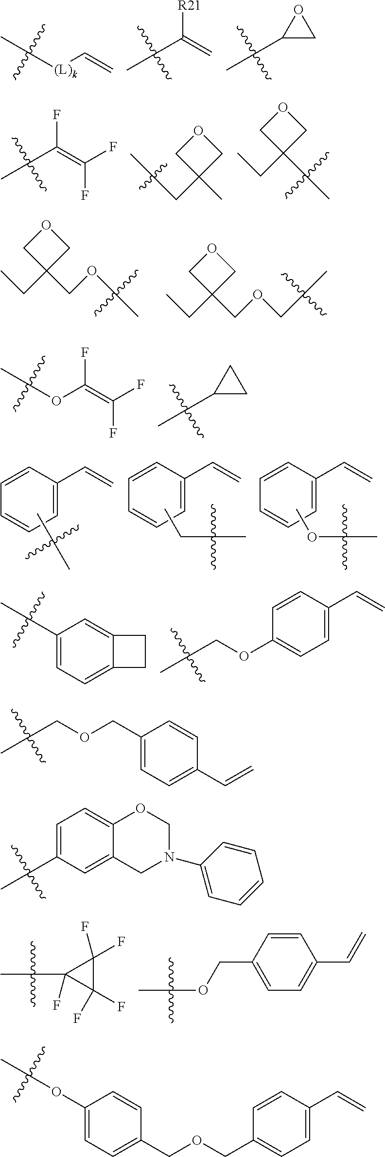
In the present specification, a “curing group” may mean a reactive substituent crosslinking compounds by being exposed to heat and/or light. The crosslinking may be produced while linking radicals produced by decomposing carbon-carbon multiple bonds or cyclic structures through heat treatment or light irradiation.
In one embodiment of the present specification, the curing group is selected from a group of the following curing groups.
[Group of Curing Groups]
Figure US11737300-20230822-C00002
In the group of the curing groups, L is a direct bond; O; S; a substituted or unsubstituted alkylene group; a substituted or unsubstituted arylene group; or a substituted or unsubstituted divalent heterocyclic group,
k is an integer of 1 or 2, and when k is 2, substituents in the parentheses are the same as or different from each other, and
R21 is a substituted or unsubstituted alkyl group.
In one embodiment of the present specification, various curing groups may be used as the curing group as long as it is a curing group capable of curing, and the curing group is not limited to the group of the curing groups.
In one embodiment of the present specification, L is a direct bond, a methylene group or an ethylene group.
In one embodiment of the present specification, L is a direct bond.
In one embodiment of the present specification, L is a methylene group.
In one embodiment of the present specification, R21 is a methyl group or an ethyl group.
In one embodiment of the present specification, R21 is a methyl group.
In the present specification, an onium compound means a compound produced through hydrogen ions or other organic radicals coordinate bonding to an unshared electron pair such as iodine, oxygen, sulfur, nitrogen or phosphorous.
Hereinafter, substituents of the present specification will be described below in detail, however, the substituents are not limited thereto.
In the present specification,
Figure US11737300-20230822-C00003

means a site bonding to other substituents or bonding sites.
The term “substitution” in the present specification means a hydrogen atom bonding to a carbon atom of a compound is changed to another substituent, and the position of substitution is not limited as long as it is a position at which the hydrogen atom is substituted, that is, a position at which a substituent can substitute, and when two or more substituents substitute, the two or more substituents may be the same as or different from each other.
The term “substituted or unsubstituted” in the present specification means being substituted with one or more substituents selected from the group consisting of hydrogen; deuterium; a halogen group; an alkyl group; a cycloalkyl group; an alkoxy group; an aryloxy group; an aryl group; an amine group; an arylamine group; and a curing group, or being unsubstituted, or being substituted with a substituent linking two or more substituents among the substituents illustrated above, or being unsubstituted.
In the present specification, examples of the halogen group may include fluorine, chlorine, bromine or iodine.
In the present specification, the alkyl group may be linear, branched or cyclic, and although not particularly limited thereto, the number of carbon atoms is preferably from 1 to 50. Specific examples thereof may include methyl, ethyl, propyl, n-propyl, isopropyl, butyl, n-butyl, isobutyl, tert-butyl, sec-butyl, 1-methyl-butyl, 1-ethyl-butyl, pentyl, n-pentyl, isopentyl, neopentyl, tert-pentyl, hexyl, n-hexyl, 1-methylpentyl, 2-methylpentyl, 4-methyl-2-pentyl, 3,3-dimethylbutyl, 2-ethylbutyl, heptyl, n-heptyl, 1-methylhexyl, cyclopropyl, cyclobutyl, cyclopentyl, 3-methylcyclopentyl, 2,3-dimethylcyclopentyl, cyclohexyl, 3-methylcyclohexyl, 4-methylcyclohexyl, 2,3-dimethylcyclohexyl, 3,4,5-trimethylcyclohexyl, 4-tert-butylcyclohexyl, cycloheptyl, cyclooctyl, octyl, n-octyl, tert-octyl, 1-methylheptyl, 2-ethylhexyl, 2-propylpentyl, n-nonyl, 2,2-dimethylheptyl, 1-ethyl-propyl, 1,1-dimethyl-propyl, isohexyl, 2-methylpentyl, 4-methylhexyl, 5-methylhexyl and the like, but are not limited thereto.
In the present specification, the alkoxy group may be linear, branched or cyclic. The number of carbon atoms of the alkoxy group is not particularly limited, but is preferably from 1 to 30. Specific examples thereof may include methoxy, ethoxy, n-propoxy, isopropoxy, i-propyloxy, n-butoxy, isobutoxy, tert-butoxy, sec-butoxy, n-pentyloxy, neopentyloxy, isopentyloxy, n-hexyloxy, 3,3-dimethylbutyloxy, 2-ethylbutyloxy, n-octyloxy, n-nonyloxy, n-decyloxy, benxyloxy, p-methylbenxyloxy and the like, but are not limited thereto.
The alkyl group may be substituted with an aryl group or a heterocyclic group to function as an arylalkyl group or a heteroarylalkyl group. The aryl group and the heterocyclic group may be selected from among examples of an aryl group or a heterocyclic group to describe below.
In the present specification, the length of the alkyl group does not affect a conjugation length of the compound, and may affect the use of the compound in an organic light emitting device, for example, the use such as a vacuum deposition method or a solution coating method.
In the present specification, the cycloalkyl group is not particularly limited, but preferably has 3 to 60 carbon atoms, and specific examples thereof may include cyclopropyl, cyclobutyl, cyclopentyl, 3-methylcyclopentyl, 2,3-dimethylcyclopentyl, cyclohexyl, 3-methylcyclohexyl, 4-methylcyclohexyl, 2,3-dimethylcyclohexyl, 3,4,5-trimethylcyclohexyl, 4-tert-butylcyclohexyl, cycloheptyl, cyclooctyl and the like, but are not limited thereto.
When the aryl group is a monocyclic aryl group in the present specification, the number of carbon atoms is not particularly limited, but is preferably from 6 to 25. Specific examples of the monocyclic aryl group may include a phenyl group, a biphenyl group, a terphenyl group, a quaterphenyl group and the like, but are not limited thereto.
When the aryl group is a multicyclic aryl group, the number of carbon atoms is not particularly limited, but is preferably from 10 to 30. Specific examples of the multicyclic aryl group may include a naphthyl group, an anthracenyl group, a phenanthryl group, a pyrenyl group, a perylenyl group, a chrysenyl group, a fluorenyl group and the like, but are not limited thereto.
In the present specification, the fluorenyl group may be substituted, and adjacent substituents may bond to each other to form a ring.
When the fluorenyl group is substituted,
Figure US11737300-20230822-C00004

and the like may be included. However, the structure is not limited thereto.
The aryl group may be substituted with an alkyl group or an alkoxy group to function as an arylalkyl group or an aryloxy group. The alkyl group or the alkoxy group may be selected from among the examples described above.
In the present specification, the number of carbon atoms of the amine group is not particularly limited, but is preferably from 1 to 30. The amine group may be substituted with the above-described alkyl group, aryl group, heterocyclic group, alkenyl group, cycloalkyl group, combinations thereof, and the like, and specific examples of the amine group may include a methylamine group, a dimethylamine group, an ethylamine group, a diethylamine group, a phenylamine group, a naphthylamine group, a biphenylamine group, an anthracenylamine group, a 9-methyl-anthracenylamine group, a diphenylamine group, a phenylnaphthylamine group, a ditolylamine group, a phenyltolylamine group, a triphenylamine group and the like, but are not limited thereto.
In the present specification, examples of the arylamine group include a substituted or unsubstituted monoarylamine group, a substituted or unsubstituted diarylamine group, or a substituted or unsubstituted triarylamine group. The aryl group in the arylamine group may be a monocyclic aryl group or a multicyclic aryl group. The arylamine group including two or more aryl groups may include monocyclic aryl groups, multicyclic aryl groups, or both monocyclic aryl groups and multicyclic aryl groups. For example, the aryl group in the arylamine group may be selected from among the examples of the aryl group described above. Specific examples of the arylamine group may include phenylamine, naphthylamine, biphenylamine, anthracenylamine, 3-methyl-phenylamine, 4-methyl-naphthylamine, 2-methyl-biphenylamine, 9-methyl-anthracenylamine, a diphenylamine group, a phenylnaphthylamine group, a ditolylamine group, a phenyltolylamine group, carbazole, a triphenylamine group and the like, but are not limited thereto.
In the present specification, the heterocyclic group includes one or more atoms that are not carbon, that is, heteroatoms, and specifically, the heteroatom may include one or more atoms selected from the group consisting of O, N, Se, S and the like. The number of carbon atoms is not particularly limited, but is preferably from 2 to 30, and the heteroaryl group may be monocyclic or multicyclic. Examples of the heterocyclic group may include a thiophene group, a furanyl group, a pyrrole group, an imidazolyl group, a thiazolyl group, an oxazolyl group, an oxadiazolyl group, a pyridyl group, a bipyridyl group, a pyrimidyl group, a triazinyl group, a triazolyl group, an acridyl group, a pyridazinyl group, a pyrazinyl group, a quinolinyl group, a quinazolinyl group, a quinoxalinyl group, a phthalazinyl group, a pyridopyrimidyl group, a pyridopyrazinyl group, a pyrazinopyrazinyl group, an isoquinolinyl group, an indolyl group, a carbazolyl group, a benzoxazolyl group, a benzimidazolyl group, a benzothiazolyl group, a benzocarbazolyl group, a benzothiophene group, a dibenzothiophene group, a benzofuranyl group, a phenanthrolinyl group, an isoxazolyl group, a thiadiazolyl group, a phenothiazinyl group, a dibenzofuranyl group and the like, but are not limited thereto.
In the present specification, the arylene group means the aryl group having two bonding sites, that is, a divalent group. Descriptions on the aryl group provided above may be applied thereto except for each being a divalent.
In the present specification, the divalent heterocyclic group means the heterocyclic group having two bonding sites, that is, a divalent group. Descriptions on the heterocyclic group provided above may be applied thereto except for each being a divalent.
In the present specification, an “adjacent” group may mean a substituent substituting an atom directly linked to an atom substituted by the corresponding substituent, a substituent sterically most closely positioned to the corresponding substituent, or another substituent substituting an atom substituted by the corresponding substituent. For example, two substituents substituting ortho positions in a benzene ring, and two substituents substituting the same carbon in an aliphatic ring may be interpreted as groups “adjacent” to each other.
In the present specification, the ring formed by adjacent groups bonding to each other may be monocyclic or multicyclic, may be aliphatic, aromatic, or a fused ring of aliphatic or aromatic, and may form a hydrocarbon ring or a heteroring.
In one embodiment of the present specification, the number of the curing group of the anion group represented by Chemical Formula 1 is 1.
In one embodiment of the present specification, the number of the curing group of the anion group represented by Chemical Formula 1 is 2.
In one embodiment of the present specification, the number of the curing group of the anion group represented by Chemical Formula 1 is 4. When the anion group represented by Chemical Formula 1 does not have a curing group, curing does not occur, and device properties may decline due to migration of a cation group and an anion group of the present specification between electrode layers. In addition, as the number of the curing group increases, a coating composition curing rate increases and a film retention rate is enhanced, and therefore, compounds having 4 curing groups are more preferred.
In one embodiment of the present specification, the number of the F, the cyano group, or the substituted or unsubstituted fluoroalkyl group in the anion group represented by Chemical Formula 1 is from 16 to 19.
In one embodiment of the present specification, parts by weight of the F in the anion group is from 15 parts by weight to 50 parts by weight or less with respect to 100 parts by weight of the anion group.
In one embodiment of the present specification, parts by weight of the F in the anion group is from 10 parts by weight to 45 parts by weight or less.
In one embodiment of the present specification, the number of the F in the anion group is from 8 to 20.
In one embodiment of the present specification, the ionic compound including the anion group may be used in a hole injection layer of an organic light emitting device, and, when used in the hole injection layer, may be used as a dopant. Herein, when the F content of the anion group increases, an electron attracting force from other compounds (host compound) increases, and holes are more favorably formed in the host resulting in performance enhancement in the hole injection layer.
In one embodiment of the present specification, the F content may be analyzed using a COSA AQF-100 combustion furnace coupled to a Dionex ICS 2000 ion-chromatograph, or may be identified through 19F NMR, a method generally used for F analysis.
In one embodiment of the present specification, at least one benzene ring among the R1 to R5-bonding benzene ring, the R6 to R10-bonding benzene ring, the R11 to R15-bonding benzene ring, and the R16 to R20-bonding benzene ring in Chemical Formula 1 is selected from among the following structural formulae.
Figure US11737300-20230822-C00005
In one embodiment of the present specification, at least one benzene ring among the R1 to R5-bonding benzene ring, the R6 to R10-bonding benzene ring, the R11 to R15-bonding benzene ring, and the R16 to R20-bonding benzene ring in Chemical Formula 1 is selected from among the following structural formulae.
Figure US11737300-20230822-C00006
In one embodiment of the present specification, the anion group is selected from among the following structural formulae.
Figure US11737300-20230822-C00007
Figure US11737300-20230822-C00008
Figure US11737300-20230822-C00009
Figure US11737300-20230822-C00010
In the structural formulae, n is an integer of 1 to 3, m is an integer of 1 to 3, and m+n=4,
q is an integer of 0 to 3, r is an integer of 1 to 4, and q+r=4,
Z is deuterium; a halogen group; a nitro group; a cyano group; an amino group; —C(O)R100; —OR101; —SR102; —SO3R103; —COOR104; —OC(O)R105; —C(O)NR106R107; a substituted or unsubstituted alkyl group; a substituted or unsubstituted alkenyl group; a substituted or unsubstituted alkynyl group; a substituted or unsubstituted amine group; a substituted or unsubstituted aryl group; or a substituted or unsubstituted heterocyclic group,
1 is an integer of 1 to 4, and when 1 is 2 or greater, Zs are the same as or different from each other, and
R100 to R107 are the same as or different from each other, and each independently hydrogen; deuterium; or a substituted or unsubstituted alkyl group.
In one embodiment of the present specification, the ionic compound includes a cation group, and the cation group is selected from among monovalent cation groups, onium compounds or the following structural formulae.
Figure US11737300-20230822-C00011
In the structural formulae, X1 to X76 are the same as or different from each other, and each independently hydrogen; a cyano group; a nitro group; a halogen group; —COOR104; a substituted or unsubstituted alkyl group; a substituted or unsubstituted alkoxy group; a substituted or unsubstituted cycloalkyl group; a substituted or unsubstituted fluoroalkyl group; or a substituted or unsubstituted aryl group, or a curing group,
R104 is hydrogen; deuterium; or a substituted or unsubstituted alkyl group,
p is an integer of 0 to 10, and
a is 1 or 2, b is 0 or 1, and a+b=2.
In one embodiment of the present specification, X1 to X76 are the same as or different from each other, and each independently hydrogen; a cyano group; a nitro group; F; Cl; —COOR104; a methyl group; an ethyl group; a propyl group; a butyl group; a pentyl group; a hexyl group; a methoxy group; a cyclopropyl group; ethoxy group; a phenyl group; a naphthyl group; or a curing group, and R104 is a methyl group.
In one embodiment of the present specification, the monovalent cation group may include Na+, Li+, K+ and the like, but is not limited thereto.
In one embodiment of the present specification, the cation group is represented by any one of the following Chemical Formula 10 to Chemical Formula 15.
Figure US11737300-20230822-C00012
In Chemical Formulae 10 to 15, X100 to X142 are the same as or different from each other, and each independently hydrogen; a cyano group; a nitro group; a halogen group; —COOR104; a substituted or unsubstituted alkyl group; a substituted or unsubstituted alkoxy group; a substituted or unsubstituted cycloalkyl group; a substituted or unsubstituted fluoroalkyl group; a substituted or unsubstituted aryl group; or a curing group, and
R104 is a substituted or unsubstituted alkyl group.
In one embodiment of the present specification, X100 to X142 are the same as or different from each other, and each independently hydrogen; a cyano group; a nitro group; F; Cl; —COOR104; a methyl group; an ethyl group; a propyl group; a butyl group; a pentyl group; a hexyl group; a methoxy group; a cyclopropyl group; ethoxy group; a phenyl group; a naphthyl group; a quinoline group; or a curing group, and R104 is a methyl group.
In one embodiment of the present specification, the cation group is selected from among the following structural formulae.
Figure US11737300-20230822-C00013
Figure US11737300-20230822-C00014
Figure US11737300-20230822-C00015
Figure US11737300-20230822-C00016
Figure US11737300-20230822-C00017
In one embodiment of the present specification, the ionic compound is selected from among the following structural formulae.
Figure US11737300-20230822-C00018
Figure US11737300-20230822-C00019
Figure US11737300-20230822-C00020
Figure US11737300-20230822-C00021
Figure US11737300-20230822-C00022
Figure US11737300-20230822-C00023
Figure US11737300-20230822-C00024
Figure US11737300-20230822-C00025
Figure US11737300-20230822-C00026
Figure US11737300-20230822-C00027
Figure US11737300-20230822-C00028
Figure US11737300-20230822-C00029
Figure US11737300-20230822-C00030
In one embodiment of the present specification, the anion group represented by Chemical Formula 1 and the cation group are included in an equivalent ratio of 1:5 to 5:1 in the ionic compound including the anion group represented by Chemical Formula 1.
In one embodiment of the present specification, the anion group represented by Chemical Formula 1 and the cation group are included in an equivalent ratio of 1:1 in the ionic compound including the anion group represented by Chemical Formula 1.
In one embodiment of the present specification, the coating composition may be a liquid phase. The “liquid phase” means in a liquid state at room temperature and atmospheric pressure.
In one embodiment of the present specification, examples of the solvent may include chlorine-based solvents such as chloroform, methylene chloride, 1,2-dichloroethane, 1,1,2-trichloroethane, chlorobenzene or o-dichlorobenzene; ether-based solvents such as tetrahydrofuran or dioxane; aromatic hydrocarbon-based solvents such as toluene, xylene, trimethylbenzene or mesitylene; aliphatic hydrocarbon-based solvents such as cyclohexane, methylcyclohexane, n-pentane, n-hexane, n-heptane, n-octane, n-nonane or n-decane; ketone-based solvents such as acetone, methyl ethyl ketone or cyclohexanone; ester-based solvents such as ethyl acetate, butyl acetate or ethyl cellosolve acetate; polyalcohols such as ethylene glycol, ethylene glycol monobutyl ether, ethylene glycol monoethyl ether, ethylene glycol monomethyl ether, dimethoxyethane, propylene glycol, diethoxymethane, triethylene glycol monoethyl ether, glycerin or 1,2-hexanediol, and derivatives thereof; alcohol-based solvents such as methanol, ethanol, propanol, isopropanol or cyclohexanol; sulfoxide-based solvents such as dimethyl sulfoxide; amide-based solvents such as N-methyl-2-pyrrolidone or N,N-dimethylformamide; benzoate-based solvents such as methyl benzoate, butyl benzoate or 3-phenoxybenzoate; tetraline, and the like, however, the solvent is not limited as long as it is a solvent capable of dissolving or dispersing the compound according to one embodiment of the present disclosure.
In another embodiment, the solvent may be used either alone as one type, or as a mixture mixing two or more solvent types.
In another embodiment, the solvent preferably has a boiling point of 40° C. to 250° C., and more preferably 60° C. to 230° C., however, the boiling point is not limited thereto.
In another embodiment, the single or mixed solvent preferably has viscosity of 1 CP to 10 CP, and more preferably 3 CP to 8 CP, however, the viscosity is not limited thereto.
In another embodiment, the coating composition preferably has a concentration of 0.1 wt/v % to 20 wt/v %, and more preferably 0.5 wt/v % to 5 wt/v %, however, the concentration is not limited thereto.
In one embodiment of the present specification, the coating composition may further include one, two or more types of additives selected from the group consisting of thermal polymerization initiators and photopolymerization initiators.
Examples of the thermal polymerization initiator may include peroxides such as methyl ethyl ketone peroxide, methyl isobutyl ketone peroxide, acetylacetone peroxide, methylcyclohexanone peroxide, cyclohexanone peroxide, isobutyryl peroxide, 2,4-dichlorobenzoyl peroxide, bis-3,5,5-trimethyl hexanoyl peroxide, lauryl peroxide, benzoyl peroxide, p-chlorobenzoyl peroxide, dicumyl peroxide, 2,5-dimethyl-2,5-(t-butyloxy)-hexane, 1,3-bis(t-butylperoxy-isopropyl)benzene, t-butyl cumyl peroxide, di-t-butyl peroxide, 2,5-dimethyl-2,5-(di-t-butylperoxy)hexane-3, tris-(t-butylperoxy)triazine, 1,1-di-t-butylperoxy-3,3,5-trimethylcyclohexane, 1,1-di-t-butylperoxycyclohexane, 2,2-di(t-butylperoxy)butane, 4,4-di-t-butylperoxy valeric acid n-butyl ester, 2,2-bis(4,4-t-butylperoxycyclohexyl)propane, t-butyl peroxyisobutyrate, di-t-butylperoxyhexahydroterephthalate, t-butylperoxy-3,5,5-trimethylhexate, t-butyl peroxybenzoate or di-t-butyl peroxytrimethyl adipate; or azo-based such as azobis isobutylnitrile, azobis dimethylvaleronitrile or azobis cyclohexyl nitrile, but are not limited thereto.
Examples of the photopolymerization initiator may include acetophenone-based or ketal-based photopolymerization initiators such as diethoxyacetophenone, 2,2-dimethoxy-1,2-diphenyl ethan-1-one, 1-hydroxy-cyclohexyl-phenyl-ketone, 4-(2-hydroxyethoxy)phenyl-(2-hydroxy-2-propyl)ketone, 2-benzyl-2-dimethylamino-1-(4-morpholinophenyl)butanone-1,2-hydroxy-2-methyl-1-phenylpropan-1-one, 2-methyl-2-morpholino(4-methylthiophenyl)propan-1-one or 1-phenyl-1,2-propanedion-2-(o-ethoxycarbonyl)oxime; benzoin ether-based photopolymerization initiators such as benzoin, benzoin methyl ether, benzoin ethyl ether, benzoin isobutyl ether or benzoin isopropyl ether; benzophenone-based photopolymerization initiators such as benzophenone, 4-hydroxybenzophenone, 2-benzoylnaphthalene, 4-benzoylbiphenyl, 4-benzoyl phenyl ether, acrylated benzophenone or 1,4-benzoylbenzene; thioxanthone-based photopolymerization initiators such as 2-isopropylthioxanthone, 2-chlorothioxanthone, 2,4-dimethylthioxanthone, 2,4-diethylthioxanthone or 2,4-dichlorothioxanthone; and, as other photopolymerization initiators, ethyl anthraquinone, 2,4,6-trimethylbenzoyldiphenylphosphine oxide, 2,4,6-trimethylbenzoylphenylethoxyphosphine oxide, bis(2,4,6-trimethylbenzoyl)phenylphosphine oxide, bis(2,4-dimethoxybenzoyl)-2,4,4-trimethylpentylphosphine oxide, methylphenylglyoxyester, 9,10-phenanthrene, acridine-based compounds, triazine-based compounds, imidazole-based compounds, and the like. In addition, those having a photopolymerization facilitating effect may be used either alone or together with the photopolymerization initiator. Examples thereof may include triethanolamine, methyldiethanolamine, ethyl 4-dimethylaminobenzoate, isoamyl 4-dimethylaminobenzoate, (2-dimethylamino)ethyl benzoate, 4,4′-dimethylaminobenzophenone and the like, but are not limited thereto.
Another embodiment of the present specification provides an organic light emitting device formed using the coating composition.
In one embodiment of the present specification, the organic light emitting device includes a first electrode; a second electrode; and one or more organic material layers provided between the first electrode and the second electrode, wherein one or more layers of the organic material layers are formed using a coating composition including the ionic compound including the anion group of Chemical Formula 1.
In one embodiment of the present specification, the organic light emitting device includes a first electrode; a second electrode; and one or more organic material layers provided between the first electrode and the second electrode, wherein one or more layers of the organic material layers include a cured material of a coating composition including the ionic compound including the anion group of Chemical Formula 1.
In one embodiment of the present specification, the cured material of the coating composition is in a cured state by heat treating or light treating the coating composition.
In one embodiment of the present specification, the organic material layer including the cured material of the coating composition is a hole injection layer.
In one embodiment of the present specification, the organic material layer including the cured material of the coating composition is a hole injection layer, and the ionic compound including the anion group of Chemical Formula 1 is included as a dopant of the hole injection layer.
In one embodiment of the present specification, the organic material layer including the cured material of the coating composition is a hole injection layer, and the ionic compound of the cured material of the coating composition is included as a p-doping material of the hole injection layer.
In one embodiment of the present specification, the organic material layer including the cured material of the coating composition is a hole injection layer, and the ionic compound including the anion group of Chemical Formula 1 is included as a p-doping material of the hole injection layer.
In the present specification, the p-doping material means a material enabling a host material to have a p semiconductor property. The p semiconductor property means a property receiving holes through injection or transferring holes at a highest occupied molecular orbital (HOMO) energy level, that is, a property of a material having high hole conductivity.
In one embodiment of the present specification, the organic material layer formed using the coating composition is a hole injection layer, and the ionic compound including the anion group of Chemical Formula 1 is a dopant of the hole injection layer, and an arylamine compound is included as a host of the hole injection layer.
In one embodiment of the present specification, the arylamine compound is a monomer or a polymer.
In one embodiment of the present specification, an arylamine compound that is a monomer or a polymer is further included as a host of the hole injection layer.
In one embodiment of the present specification, the arylamine compound includes one of the following-structured curing groups.
Figure US11737300-20230822-C00031
In the structural formulae, L is a direct bond; O; S; a substituted or unsubstituted alkylene group; a substituted or unsubstituted arylene group; or a substituted or unsubstituted divalent heterocyclic group, and
k is an integer of 1 or 2, and when k is 2, substituents in the parentheses are different from each other, and R21 is a substituted or unsubstituted alkyl group.
In one embodiment of the present specification, the host of the hole injection layer has a HOMO level from 4.8 eV to 5.8 eV.
The HOMO level of the present specification is measured using an electrochemical cyclic voltammetry method (CV). Onset potential (Eonset) at which host material oxidation begins is measured, and ferrocene potential (E1/2(Fc)) is measured under the same condition. The ferrocene potential is defined as 4.8 eV with respect to a vacuum energy level, and the HOMO level is calculated using the following equation.
HOMO(eV)=4.8+(E onset −E 1/2(Fc))
The arylamine compound forms crosslinking, and an organic material layer including a thin-filmed structure is capable of being provided. In this case, being dissolved by a solvent deposited on a surface of the organic material layer formed using the coating composition, or being morphologically influenced or decomposed may be prevented.
Accordingly, when the organic material layer including the cured material of the coating composition is formed including a step of heat treatment or light treatment, resistance for a solvent increases, and a multilayer may be formed by repeatedly performing solution deposition and crosslinking method, and as a result, a lifetime property of a device may be enhanced due to increased stability.
In one embodiment of the present specification, the organic material layer including the cured material of the coating composition is a hole transfer layer, a hole injection layer, or a layer carrying out hole transfer and hole injection at the same time.
In another embodiment, the organic material layer formed using the coating composition is a light emitting layer.
In one embodiment of the present specification, the organic light emitting device further includes one, two or more layers selected from the group consisting of a hole injection layer, a hole transfer layer, an electron transfer layer, an electron injection layer, an electron blocking layer and a hole blocking layer.
In one embodiment of the present specification, the first electrode is a cathode, and the second electrode is an anode.
In one embodiment of the present specification, the first electrode is an anode, and the second electrode is a cathode.
In another embodiment, the organic light emitting device may be an organic light emitting device having a structure in which an anode, one or more organic material layers and a cathode are consecutively laminated on a substrate (normal type).
In another embodiment, the organic light emitting device may be an organic light emitting device having a structure in a reverse direction in which a cathode, one or more organic material layers and an anode are consecutively laminated on a substrate (inverted type).
The organic material layer of the organic light emitting device of the present specification may be formed in a single layer structure, but may also be formed in a multilayer structure in which two or more organic material layers are laminated. For example, the organic light emitting device of the present disclosure may have a structure including a hole injection layer, a hole transfer layer, a light emitting layer, an electron transfer layer, an electron injection layer and the like as the organic material layer. However, the structure of the organic light emitting device is not limited thereto, and may include less numbers of organic material layers.
For example, a structure of the organic light emitting device according to one embodiment of the present specification is illustrated in FIG. 1 .
FIG. 1 illustrates a structure of the organic light emitting device in which an anode (201), a hole injection layer (301), a hole transfer layer (401), a light emitting layer (501), an electron transfer layer (601) and a cathode (701) are consecutively laminated on a substrate (101).
In FIG. 1 , the hole injection layer (301), the hole transfer layer (401) and the light emitting layer (501) are formed using a coating composition including the compound represented by Chemical Formula 1.
FIG. 1 illustrates the organic light emitting device, however, the organic light emitting device is not limited thereto.
When the organic light emitting device includes a plurality of organic material layers, the organic material layers may be formed with materials that are the same as or different from each other.
The organic light emitting device of the present specification may be manufactured using materials and methods known in the art, except that one or more layers of the organic material layers are formed using the coating composition including the compound.
For example, the organic light emitting device of the present specification may be manufactured by consecutively laminating an anode, an organic material layer and a cathode on a substrate. Herein, the organic light emitting device may be manufactured by forming an anode on a substrate by depositing a metal, a metal oxide having conductivity, or an alloy thereof using a physical vapor deposition (PVD) method such as sputtering or e-beam evaporation, and forming an organic material layer including a hole injection layer, a hole transfer layer, a light emitting layer and an electron transfer layer thereon, and then depositing a material capable of being used as a cathode thereon. In addition to such a method, the organic light emitting device may also be manufactured by consecutively depositing a cathode material, an organic material layer and an anode material on a substrate.
One embodiment of the present specification also provides a method for manufacturing an organic light emitting device formed using the coating composition.
Specifically, the method for manufacturing an organic light emitting device in one embodiment of the present specification includes preparing a substrate; forming a cathode or an anode on the substrate; forming one or more organic material layers on the cathode or the anode; and forming an anode or a cathode on the organic material layers, wherein one or more layers of the organic material layers are formed using the coating composition.
In one embodiment of the present specification, the organic material layer formed using the coating composition is formed using spin coating.
In another embodiment, the organic material layer formed using the coating composition is formed using a printing method.
In an embodiment of the present specification, examples of the printing method include inkjet printing, nozzle printing, offset printing, transfer printing, screen printing or the like, but are not limited thereto.
The coating composition according to one embodiment of the present specification is suited for a solution process due to its structural properties and may be formed using a printing method, and therefore, is economically effective in terms of time and costs when manufacturing a device.
In one embodiment of the present specification, the forming of an organic material layer formed using the coating composition includes coating the coating composition on the cathode or the anode; and heat treating or light treating the coated coating composition.
In one embodiment of the present specification, the time of heat treating the organic material layer formed using the coating composition is preferably within 1 hour and more preferably within 30 minutes.
In one embodiment of the present specification, the atmosphere of heat treating the organic material layer formed using the coating composition is preferably inert gas such as argon or nitrogen.
In addition, the composition according to one embodiment of the present specification may be thin-filmed through heat treatment or light treatment, and may be included as a copolymer using a coating composition mixed with other monomers. In addition, a copolymer or a mixture may be included using a coating composition mixed with other polymers.
As the anode material, materials having large work function are normally preferred so that hole injection to an organic material layer is smooth. Specific examples of the anode material capable of being used in the present disclosure include metals such as vanadium, chromium, copper, zinc and gold, or alloys thereof; metal oxides such as zinc oxide, indium oxide, indium tin oxide (ITO) and indium zinc oxide (IZO); combinations of metals and oxides such as ZnO:Al or SnO2:Sb; conductive polymers such as poly(3-methylthiophene), poly[3,4-(ethylene-1,2-dioxy)thiophene] (PEDOT), polypyrrole and polyaniline, and the like, but are not limited thereto.
As the cathode material, materials having small work function are normally preferred so that electron injection to an organic material layer is smooth. Specific examples of the cathode material include metals such as magnesium, calcium, sodium, potassium, titanium, indium, yttrium, lithium, gadolinium, aluminum, silver, tin and lead, or alloys thereof; multilayer structure materials such as LiF/Al or LiO2/Al, and the like, but are not limited thereto.
The hole injection layer is a layer that injects holes from an electrode, and the hole injection material is preferably a compound that has an ability to transfer holes, therefore, has a hole injection effect in an anode, has an excellent hole injection effect for a light emitting layer or a light emitting material, prevents excitons generated in the light emitting layer from moving to an electron injection layer or an electron injection material, and in addition, has an excellent thin film forming ability. The highest occupied molecular orbital (HOMO) of the hole injection material is preferably in between the work function of an anode material and the HOMO of surrounding organic material layers. Specific examples of the hole injection material include metal porphyrins, oligothiophene, arylamine-based organic materials, hexanitrile hexaazatriphenylene-based organic materials, quinacridone-based organic materials, perylene-based organic materials, anthraquinone, and polyaniline- and polythiophene-based conductive polymers, and the like, but are not limited thereto.
The hole transfer layer is a layer that receives holes from a hole injection layer and transfers the holes to a light emitting layer, and as the hole transfer material, materials capable of receiving holes from an anode or a hole injection layer, moving the holes to a light emitting layer, and having high mobility for the holes are suitable. Specific examples thereof include arylamine-based organic materials, conductive polymers, block copolymers having conjugated parts and non-conjugated parts together, and the like, but are not limited thereto.
The light emitting material is a material capable of emitting light in a visible light region by receiving holes and electrons from a hole transfer layer and an electron transfer layer, respectively, and binding the holes and the electrons, and is preferably a material having favorable quantum efficiency for fluorescence or phosphorescence. Specific examples thereof include 8-hydroxyquinoline aluminum complexes (Alq3); carbazole-based compounds; dimerized styryl compounds; BAlq; 10-hydroxybenzo quinoline-metal compounds; benzoxazole-, benzthiazole- and benzimidazole-based compounds; poly(p-phenylenevinylene) (PPV)-based polymers; spiro compounds; polyfluorene, rubrene, and the like, but are not limited thereto.
The light emitting layer may include a host material and a dopant material. The host material includes fused aromatic ring derivatives, heteroring-containing compounds or the like. Specifically, the fused aromatic ring derivative includes anthracene derivatives, pyrene derivatives, naphthalene derivatives, pentacene derivatives, phenanthrene compounds, fluoranthene compounds and the like, and the heteroring-containing compound includes carbazole derivatives, dibenzofuran derivatives, ladder-type furan compounds, pyrimidine derivatives and the like, however, the material is not limited thereto.
The dopant material includes aromatic amine derivatives, styrylamine compounds, boron complexes, fluoranthene compounds, metal complexes and the like. Specifically, the aromatic amine derivative is a fused aromatic ring derivative having a substituted or unsubstituted arylamino group and includes arylamino group-including pyrene, anthracene, chrysene, peryflanthene and the like, and the styrylamine compound is a compound in which substituted or unsubstituted arylamine is substituted with at least one arylvinyl group, and one, two or more substituents selected from the group consisting of an aryl group, a silyl group, an alkyl group, a cycloalkyl group and an arylamino group are substituted or unsubstituted. Specifically, styrylamine, styryldiamine, styryltriamine, styryltetramine or the like is included, however, the styrylamine compound is not limited thereto. In addition, the metal complex includes iridium complexes, platinum complexes or the like, but is not limited thereto.
The electron transfer layer is a layer that receives electrons from an electron injection layer and transfers the electrons to a light emitting layer, and as the electron transfer material, materials capable of favorably receiving electrons from a cathode, moving the electrons to a light emitting layer, and having high mobility for the electrons are suitable. Specific examples thereof include Al complexes of 8-hydroxyquinoline; complexes including Alq3; organic radical compounds; hydroxyflavon-metal complexes, and the like, but are not limited thereto. The electron transfer layer may be used together with any desired cathode material as used in the art. Particularly, examples of the suitable cathode material include common materials that have small work function, and in which an aluminum layer or a silver layer follows. Specifically, the cathode material includes cesium, barium, calcium, ytterbium and samarium, and in each case, an aluminum layer or a silver layer follows.
The electron injection layer is a layer that injects electrons from an electrode, and the electron injection material is preferably a compound that has an ability to transfer electrons, has an electron injection effect from a cathode, has an excellent electron injection effect for a light emitting layer or a light emitting material, prevents excitons generated in the light emitting layer from moving to a hole injection layer, and in addition, has an excellent thin film forming ability. Specific examples thereof include fluorenone, anthraquinodimethane, diphenoquinone, thiopyran dioxide, oxazole, oxadiazole, triazole, imidazole, perylene tetracarboxylic acid, fluorenylidene methane, anthrone or the like, and derivatives thereof, metal complex compounds, nitrogen-containing 5-membered ring derivatives, and the like, but are not limited there.
The metal complex compound includes 8-hydroxyquinolinato lithium, bis(8-hydroxyquinolinato)zinc, bis(8-hydroxyquinolinato)copper, bis(8-hydroxyquinolinato)manganese, tris(8-hydroxyquinolinato)aluminum, tris(2-methyl-8-hydroxyquinolinato)aluminum, tris(8-hydroxyquinolinato)gallium, bis(10-hydroxybenzo[h]quinolinato)berylium, bis(10-hydroxybenzo[h]quinolinato)zinc, bis(2-methyl-8-quinolinato)chlorogallium, bis(2-methyl-8-quinolinato)(o-cresolato)gallium, bis(2-methyl-8-quinolinato)(1-naphtholato)aluminum, bis(2-methyl-8-quinolinato)(2-naphtholato)gallium and the like, but is not limited thereto.
The hole blocking layer is a layer blocking holes from reaching a cathode, and generally, may be formed under the same condition as the hole injection layer. Specifically, oxadiazole derivatives or triazole derivatives, phenanthroline derivatives, BCP, aluminum complexes and the like are included, however, the material is not limited thereto.
The organic light emitting device according to the present specification may be a top-emission type, a bottom-emission type or a dual-emission type depending on the materials used.
In one embodiment of the present specification, the coating composition may be included in organic solar cells or organic transistors in addition to organic light emitting devices.
Hereinafter, the present specification will be described in detail with reference to examples in order to specifically describe the present specification. However, the examples according to the present specification may be modified to various different forms, and the scope of the present specification is not to be construed as being limited to the examples described below. Examples of the present specification are provided in order to more fully describe the present specification to those having average knowledge in the art.
EXAMPLE Preparation Example 1_Preparation of Compound 1
Figure US11737300-20230822-C00032
Under nitrogen atmosphere, Mg (193 mg, 7.9208 mmol), I2 (4 mg) and tetrahydrofuran (THF) (10 mL) were placed in a 100 mL round bottom flask, and stirred for 30 minutes. 4-Bromostyrene (1.04 mL, 7.9208 mmol) was added thereto, and the result was stirred for a day while a 30° C. water bath was placed under the round bottom flask. Dissolution of Mg was identified as the reaction solution became black. Ether (5 mL) was added thereto to dilute the reaction solution. Tris(pentafluorophenyl)borane (1 g, 3.9604 mmol) dissolved in ether (5 mL) was slowly added to the reaction solution for 30 minutes. The solution was stirred for a day. Na2CO3 (0.1 M, 80 mL, 8.0 mmol) was slowly added to the reaction solution. The organic solvent was extracted using EA (20 mL×3), and residual water was removed with MgSO4. In order to additionally remove residual water and impurities, the result was distilled with benzene using a Dean-stark. When approximately 10 mL of the solvent was left, the solution was cooled and filtered to obtain a target compound (1.6 g). (Yield: 64%)
Figure US11737300-20230822-C00033
Sodium tris(perfluorophenyl) (4-vinylphenyl)borate (100 mg, 0.1567 mmol), distilled water (10 mL) and Ph2ICl (60 mg, 0.1881 mmol) were placed in a 25 mL round bottom flask, and stirred for 1 hour. Precipitates were produced when adding acetone (15 mL) to the reaction solution, and these precipitates were filtered and dried to obtain Compound 1 (140 mg). (Yield: 100%)
Preparation Example 2_Preparation of Compound 2
Figure US11737300-20230822-C00034
Mg (95 mg, 3.9214 mmol), THF (10 mL) and I2 (4 mg) were placed in a 25 mL round bottom flask, and stirred. 1-Bromo-2,3,5,6-tetrafluoro-4-(1,2,2-trifluorovinyl)benzene (1.2 g, 3.9214 mmol) was introduced to the reaction solution, and the result was stirred at room temperature. After 10 hours, dissolution of Mg was identified by the solution becoming black, and ether (10 mL) and BCl3 (1.3 mL, 1.3 mmol, 1 M in hexane solution) were added thereto over 30 minutes. After stirring the reaction solution for a day, Na2CO3 (30 mL, 3.0 mmol, 0.1 M in H2O) was added thereto. The synthesized material was extracted using EA (3×10 mL), and then residual water was removed with MgSO4. After removing all the solvent, water was completely removed with Dean-stark using benzene, and the solids were filtered to obtain a target compound (430 mg) (Yield: 35%)
Figure US11737300-20230822-C00035
Sodium tetrakis(2,3,5,6-tetrafluoro-4-(1,2,2-trifluorovinyl)phenyl)borate (300 mg, 0.3158 mmol), diphenyliodonium chloride (100 mg, 0.3158 mmol), H2O (10 mL) and acetone (10 mL) were placed in a 25 mL round bottom flask, and vigorously stirred for 30 minutes. The result was extracted using dichloromethane (10 mL×3), and then dried after removing the solvent to obtain a target compound (381 mg). (Yield: 100%)
Preparation Example 3_Preparation of Compound 3
Figure US11737300-20230822-C00036
Mg (190 mg, 7.8428 mmol), THF (20 mL) and I2 (8 mg) were placed in a 50 mL round bottom flask, and stirred. 1-Bromo-2,3,5,6-tetrafluoro-4-(1,2,2-trifluorovinyl)benzene (2 g, 7.8428 mmol) was introduced to the reaction solution, and the result was stirred at room temperature. Mg (63 mg, 2.6142 mmol), THF (10 mL) and I2 (3 mg) were placed in another 25 mL round bottom flask, and stirred. 1-Bromo-2,3,4,5,6-pentafluorobenzene (646 mg, 2.6142 mmol) was introduced to the reaction solution, and the result was stirred at room temperature. After 10 hours, dissolution of Mg was identified by the solution becoming black, and BCl3 (2.6 mL, 2.6142 mmol, 1 M in hexane solution) was added to a 50 mL round bottom flask over 30 minutes. After 2 hours, the solution in the 25 mL round bottom flask was slowly added to the solution in the 50 mL round bottom flask using a cannula needle. After stirring the reaction solution for a day, Na2CO3 (30 mL, 3.0 mmol, 0.1 M in H2O) was added thereto. The synthesized material was extracted using EA (3×10 mL), and residual water was removed with MgSO4. After removing all the solvent, water was completely removed with Dean-stark using benzene, and the solids were filtered to obtain a target compound (800 mg) (Yield: 42%)
Figure US11737300-20230822-C00037
Sodium (perfluorophenyl)tris(2,3,5,6-tetrafluoro-4-vinylphenyl)borate (400 mg, 0.5508 mmol), diphenyliodonium chloride (174 mg, 0.5508 mmol), H2O (10 mL) and acetone (10 mL) were placed in a 25 mL round bottom flask, and vigorously stirred for 30 minutes. The result was extracted using dichloromethane (10 mL×3) and then dried after removing the solvent to obtain a target compound (542 mg). (Yield: 100%)
Preparation Example 4_Preparation of Compound 4
Figure US11737300-20230822-C00038
Methyltriphenyl potassium bromide (16 g, 45.2489 mmol) and tetrahydrofuran (THF) (100 mL) were placed in a 250 mL round bottom flask, and stirred for 30 minutes at 0° C. n-BuLi (18.1 mL, 45.2489 mmol, 2.5 M in hexane) was slowly added to the reaction solution, and the result was stirred for 30 minutes at 0° C. At 0° C., 4-bromo-2,6-difluorobenzaldehyde (5.0 g, 22.6244 mmol, in 30 mL tetrahydrofuran (THF)) was slowly added to the reaction solution. The reaction solution was stirred while slowly raising the temperature to room temperature. After 3 hours, ether (100 mL) and a saturated NH4Cl solution (400 mL) were added to the reaction solution. The organic solvent was extracted using ether (2×200 mL), and residual water was removed with MgSO4. The result was columned using EA:Hex=1:9 to obtain a target compound (3 g). (Yield: 60%)
Figure US11737300-20230822-C00039
Mg (111 mg, 4.5656 mmol), THF (10 mL) and I2 (4 mg) were placed in a 25 mL round bottom flask, and stirred. 5-Bromo-1,3-difluoro-2-vinylbenzene (1 g, 4.5656 mmol) was introduced to the reaction solution, and the result was stirred at room temperature. After 10 hours, dissolution of Mg was identified by the solution becoming black, and ether (10 mL) and BCl3 (1.1 mL, 1.0957 mmol, 1 M in hexane solution) were added thereto over 30 minutes. After stirring the reaction solution for a day, Na2CO3 (30 mL, 3.0 mmol, 0.1 M in H2O) was added thereto. The synthesized material was extracted using EA (3×10 mL), and residual water was removed with MgSO4. After removing all the solvent, water was completely removed with Dean-stark using benzene, and the solids were filtered to obtain a target compound (400 mg). (Yield: 62%)
Figure US11737300-20230822-C00040
Sodium tetrakis(3,5-difluoro-4-vinylphenyl)borate (400 mg, 0.6776 mmol), diphenyliodonium chloride (215 mg, 0.6776 mmol), H2O (10 mL) and acetone (10 mL) were placed in a 25 mL round bottom flask, and vigorously stirred for 30 minutes. The result was extracted using dichloromethane (10 mL×3), and then dried after removing the solvent to obtain a target compound (574 mg). (Yield: 100%)
Preparation Example 5_Preparation of Compound 5
Figure US11737300-20230822-C00041
Methyltriphenyl potassium bromide (13.90 g, 38.9135 mmol) and tetrahydrofuran (THF) (100 mL) were placed in a 250 mL round bottom flask, and stirred for 30 minutes at 0° C. n-BuLi (15.6 mL, 38.9135 mmol, 2.5 M in hexane) was slowly added to the reaction solution, and the result was stirred for 30 minutes at 0° C. At 0° C., 4-formyl-2,3,5,6-tetrafluoro-1-bromobenzene (5.0 g, 19.4568 mmol, in 30 mL tetrahydrofuran (THF)) was slowly added to the reaction solution. The reaction solution was stirred while slowly raising the temperature to room temperature. After 3 hours, ether (100 mL) and a saturated NH4Cl solution (400 mL) were added to the reaction solution. The organic solvent was extracted using ether (2×200 mL), and residual water was removed with MgSO4. The result was columned using EA:Hex=1:9 to obtain a target compound (1.29 g). (Yield: 26%)
Figure US11737300-20230822-C00042
Mg (95 mg, 3.9214 mmol), THF (10 mL) and I2 (4 mg) were placed in a 25 mL round bottom flask, and stirred. 1-Bromo-2,3,5,6-tetrafluoro-4-vinylbenzene (1.0 g, 3.9214 mmol) was introduced to the reaction solution, and the result was stirred at room temperature. After 10 hours, dissolution of Mg was identified by the solution becoming black, and ether (10 mL) and BCl3 (1.3 mL, 1.3 mmol, 1 M in hexane solution) were added thereto over 30 minutes. After stirring the reaction solution for a day, Na2CO3 (30 mL, 3.0 mmol, 0.1 M in H2O) was added thereto. The synthesized material was extracted using EA (3×10 mL), and residual water was removed with MgSO4. After removing all the solvent, water was completely removed with Dean-stark using benzene, and the solids were filtered to obtain a target compound (340 mg). (Yield: 28%)
Figure US11737300-20230822-C00043
Sodium tetrakis (2,3,5,6-tetrafluoro-4-vinylphenyl) borate (200 mg, 0.2724 mmol), 1-(4-vinylbenzyl)pyridin-1-ium chloride (69 mg, 0.2996 mmol), H2O (10 mL) and MC (10 mL) were placed in a 25 mL round bottom flask, and vigorously stirred for 30 minutes. The organic solvent was extracted using ether (3×10 mL), and residual water was removed with MgSO4. The solvent was removed, and the result was vacuum dried to obtain Compound 5 (247 mg). (Yield: 100%)
Preparation Example 6 Preparation of Compound 6
Figure US11737300-20230822-C00044
In a 50 mL round bottom flask, 1-bromo-2,3,5,6-tetrafluoro-4-(1,2,2-trifluorovinyl)benzene (2 g, 7.8428 mmol) was introduced to THF (20 mL), and the result was stirred for 30 minutes under a −78° C. condition. To the solution, n-BuLi in hexane (3.45 mL, 8.6271 mmol, 2.5 M) was slowly introduced, and the result was stirred for 30 minutes at −78° C. To the reaction solution, BCl3 (2.6 mL, 2.6142 mmol, 1 M in hexane solution) was added over 15 minutes at −78° C. The reaction solution was stirred for a day while slowly raising the temperature to room temperature, and water (30 mL) was added thereto. The synthesized material was extracted using EA (3×10 mL), and all the solvent was removed. Water was completely removed with Dean-stark using benzene, and the solids were filtered to obtain a target compound (800 mg). (Yield: 43%)
An NMR spectrum of the compound is shown in FIG. 10 .
A mass spectrum of the compound is shown in FIG. 11 .
Figure US11737300-20230822-C00045
Lithium (perfluorophenyl)tris(2,3,5,6-tetrafluoro-4-vinylphenyl)borate (400 mg, 0.5569 mmol), diphenyliodonium chloride (176 mg, 0.5569 mmol), H2O (10 mL) and acetone (10 mL) were placed in a 25 mL round bottom flask, and vigorously stirred for 30 minutes. The result was extracted using dichloromethane (10 mL×3), and then dried after removing the solvent to obtain target Compound 6 (552 mg). (Yield: 100%)
MS data of Compound 6 are shown in FIG. 2 , DSC data of Compound 6 are shown in FIG. 3 , and an NMR spectrum of Compound 6 is shown in FIG. 4 .
The DSC data are differential scanning calorimeter data, and curing of the dopant material was seen through FIG. 3 .
Preparation Example 7_Preparation of Compound 7
Figure US11737300-20230822-C00046
Potassium carbonate (10.4 g, 75.3 mmol) and then dimethylformamide (DMF) (200 ml) were placed in a 500 mL round bottom flask. To the flask, 2,3,5,6-tetrafluorophenol (10.0 g, 60.22 mmol) was introduced, and the result was stirred for 30 minutes at 60° C. 4-Vinylbenzyl chloride (7.66 g, 50.18 mmol) was slowly added to the reaction solution, and the result was stirred for 16 hours at 60° C. After that, H2O (300 mL) and EA (200 ml) were added. The organic layer was extracted using EA (2×200 mL), and residual water was removed with MgSO4. The result was columned using EA:Hex=1:9 to obtain a target compound (11.2 g). (Yield: 79%)
Figure US11737300-20230822-C00047
After placing 1,2,4,5-tetrafluoro-3-((4-vinylbenzyl)oxy)benzene (10 g, 35.43 mmol) in a 250 ml round bottom flask, ether (130 ml) was introduced thereto, and the result was stirred. The reaction solution was cooled to −78° C., and stirred for 30 minutes. n-BuLi (17 ml, 42.52 mmol, 2.5 M in hexane) was slowly injected thereto over 30 minutes. After that, the result was stirred for 1 hour. BCl3 (8.15 ml, 8.15 mmol, 1 M in hexane) was slowly introduced thereto over 30 minutes. After that, the result was further stirred for 2 hours, and the temperature of the reaction solution was slowly raised to room temperature. After stirring the reaction solution for a day, H2O (200 ml) was added thereto. The synthesized material was extracted using ether (3×100 mL), and all the solvent was removed. After that, water was completely removed with Dean-stark using benzene, and the solids were filtered to obtain a target compound (6.2 g). (Yield: 66%)
Figure US11737300-20230822-C00048
Lithium tetrakis (2,3,5,6-tetrafluoro-4-((4-vinylbenzyl)oxy)phenyl)borate (6.2 g, 5.42 mmol), diphenyliodonium chloride (2.57 g, 8.13 mmol), H2O (50 mL) and acetone (10 mL) were placed in a 25 mL round bottom flask, and vigorously stirred for 30 minutes. The organic solvent was extracted using MC (3×20 mL), and the solvent was removed. The result was columned using MC:acetone=9:1 to obtain target Compound 7 (5.0 g). (Yield: 65%)
An NMR spectrum of Compound 7 is shown in FIG. 9 .
Preparation Example 8_Preparation of Compound 8
Figure US11737300-20230822-C00049
1-Bromo-2,3,5,6-tetrafluoro-4-(1,2,2-trifluorovinyl)benzene (3 g, 9.7093 mmol) and hexafluoropropylene oxide (3 g, 18.0701 mmol) were placed in a 15 mL stainless steel cylinder, and heated for 4 hours at 190° C. After slowly cooling the container, the solution inside the container was washed 3 times with water (5 mL). The organic solution was dried using magnesium sulfate. This mixture was silica column purified using a 9:1 hexane:ethyl acetate solvent to obtain a target compound (1.2 g) (Yield: 34%)
Figure US11737300-20230822-C00050
Mg (81 mg, 3.3427 mmol), THF (10 mL) and I2 (4 mg) were placed in a 25 mL round bottom flask, and stirred. 1-Bromo-2,3,5,6-tetrafluoro-4-(perfluorocyclopropyl)benzene (1.2 g, 3.3427 mmol) was introduced to the reaction solution, and the result was stirred at room temperature. After 10 hours, complete dissolution of Mg was identified by the solution becoming black, and ether (10 mL) and BCl3 (0.8 mL, 0.8022 mmol, 1 M in heptane solution) were added thereto over 30 minutes. After stirring the reaction solution for a day, Na2CO3 (30 mL, 3.0 mmol, 0.1 M in H2O) was added thereto. The synthesized material was extracted using EA (3×10 mL), and then residual water was removed with MgSO4. After removing all the solvent, water was completely removed with Dean-stark using benzene, and the solids were filtered to obtain a target compound (410 mg). (Yield: 44%)
Figure US11737300-20230822-C00051
Sodium tetrakis (2,3,5,6-tetrafluoro-4-(perfluorocyclopropyl)phenyl)borate (501 mg, 0.6823 mmol), diphenyliodonium chloride (216 mg, 0.6823 mmol), H2O (10 mL) and acetone (10 mL) were placed in a 25 mL round bottom flask, and vigorously stirred for 30 minutes. When precipitates were produced, the precipitates were washed with water to obtain target Compound 8 (960 mg). (Yield: 100%)
Preparation Example 9 Preparation of Compound 9
Figure US11737300-20230822-C00052
Mg (95 mg, 3.9214 mmol), THF (10 mL) and I2 (4 mg) were placed in a 25 mL round bottom flask, and stirred. 1-Bromo-2,3,5,6-tetrafluoro-4-vinylbenzene (1.0 g, 3.9214 mmol) was introduced to the reaction solution, and the result was stirred at room temperature. After 10 hours, dissolution of Mg was identified by the solution becoming black, and ether (10 mL) and tris(pentafluorophenyl)borane (2 g, 3.9214 mmol) were added thereto over 30 minutes. After stirring the reaction solution for a day, Na2CO3 (30 mL, 3.0 mmol, 0.1 M in H2O) was added thereto. The synthesized material was extracted using EA (3×10 mL), and then residual water was removed with MgSO4. After removing all the solvent, water was completely removed with Dean-stark using benzene, and the solids were filtered to obtain a target compound (1.2 g). (Yield: 43%)
Figure US11737300-20230822-C00053
Sodium tris(perfluorophenyl) (2,3,5,6-tetrafluoro-4-vinylphenyl)borate (500 mg, 0.7041 mmol), diphenyliodonium chloride (223 mg, 0.7041 mmol), H2O (10 mL) and acetone (10 mL) were placed in a 25 mL round bottom flask, and vigorously stirred for 30 minutes. When precipitates were produced, the precipitates were washed with water to obtain target Compound 9 (660 mg). (Yield: 97%)
Preparation Example 10_Preparation of Compound 10
Figure US11737300-20230822-C00054
(4-Bromo-2,6-bis(trifluoromethyl)phenyl)methanol (4 g, 12.3828 mmol), phosphorous pentoxide (290 mg, 3.7148 mmol) and hydroquinone (82 mg, 0.7430 mmol) were placed in a 25 mL round bottom flask, and stirred for 1 hour at 160° C. After cooling the reaction solution to room temperature, a saturated aqueous sodium bicarbonate solution (15 mL) was slowly added thereto. The synthesized material was extracted using MC (3×10 mL), and residual water was removed with MgSO4. After removing the MC solvent, the result was purified using silica gel column chromatography (10% ethyl acetate/hexane), and dried to obtain a target compound (2.6 g). (Yield: 65%)
Figure US11737300-20230822-C00055
Mg (198 mg, 8.1494 mmol), THF (20 mL) and I2 (8 mg) were placed in a 100 mL round bottom flask, and stirred. 5-Bromo-1,3-bis(trifluoromethyl)-2-vinylbenzene (2.6 g, 8.1494 mmol) was introduced to the reaction solution, and the result was stirred at room temperature. After 10 hours, dissolution of Mg was identified by the solution becoming black, and ether (20 mL) and BCl3 (2.0 mL, 1.9559 mmol, 1 M in hexane solution) were added thereto over 30 minutes. After stirring the reaction solution for a day, Na2CO3 (40 mL, 3.0 mmol, 0.1 M in H2O) was added thereto. The synthesized material was extracted using EA (3×20 mL), and residual water was removed with MgSO4. After removing all the solvent, water was completely removed with Dean-stark using benzene, and the solids were filtered to obtain a target compound (1.1 g). (Yield: 59%)
Figure US11737300-20230822-C00056
Sodium tetrakis(3,5-bis(trifluoromethyl)-4-vinylphenyl)borate (2 g, 2.0195 mmol), diphenyliodonium chloride (639 mg, 2.0195 mmol), H2O (20 mL) and acetone (20 mL) were placed in a 50 mL round bottom flask, and vigorously stirred for 30 minutes. The result was extracted using dichloromethane (20 mL×3), and then dried after removing the solvent to obtain a target compound (2.5 g). (Yield: 100%)
Experimental Example 1-1. Formation of Coating Layer Using Coating Composition
The coating composition was mixed as described in the following Table 1, and specifically, Coating Composition 1 was produced by mixing a p-doping material represented by the following Compound 1, a host compound that is the following [Compound A], and an organic solvent (cyclohexanone). Specifically, Compound 1, Compound A and the organic solvent were mixed in a weight ratio of 2:8:490 to produce the coating composition, and Coating Composition 1 was spin coated to form a coating layer, and the film was baked at 250° C. or lower.
Coating Composition 2 was produced in the same manner as Coating Composition 1 except that the following Compound 2 was used instead of Compound 1 of the present disclosure. Coating Composition 2 was spin coated to form a coating layer, and the film was baked at 250° C. or lower.
Coating Composition 3 was produced in the same manner as Coating Composition 1 except that the following Compound 3 was used instead of Compound 1 of the present disclosure. Coating Composition 3 was spin coated to form a coating layer, and the film was baked at 250° C. or lower.
Coating Composition 4 was produced in the same manner as Coating Composition 1 except that the following Compound 4 was used instead of Compound 1 of the present disclosure. Coating Composition 4 was spin coated to form a coating layer, and the film was baked at 250° C. or lower.
Coating Composition 5 was produced in the same manner as Coating Composition 1 except that the following Compound 5 was used instead of Compound 1 of the present disclosure. Coating Composition 5 was spin coated to form a coating layer, and the film was baked at 250° C. or lower.
Coating Composition 6 was produced in the same manner as Coating Composition 1 except that the following Compound 6 was used instead of Compound 1 of the present disclosure. Coating Composition 6 was spin coated to form a coating layer, and the film was baked at 250° C. or lower.
Coating Composition 7 was produced in the same manner as Coating Composition 6 except that the following [Compound B] was used instead of the host compound [Compound A]. Coating Composition 7 was spin coated to form a coating layer, and the film was baked at 250° C. or lower.
Coating Composition 8 was produced in the same manner as Coating Composition 6 except that the following [Compound C] was used instead of the host compound [Compound A]. Coating Composition 8 was spin coated to form a coating layer, and the film was baked at 250° C. or lower.
Coating Composition 9 was produced in the same manner as Coating Composition 1 except that the following Compound 9 was used instead of Compound 1 of the present disclosure. Coating Composition 9 was spin coated to form a coating layer, and the film was baked at 250° C. or lower.
Coating Composition 10 was produced in the same manner as Coating Composition 1 except that the following Compound 10 was used instead of Compound 1 of the present disclosure. Coating Composition 10 was spin coated to form a coating layer, and the film was baked at 250° C. or lower.
Coating Composition 11 was produced in the same manner as Coating Composition 1 except that the following Comparative Compound 1 was used instead of Compound 1 of the present disclosure. Coating Composition 11 was spin coated to form a coating layer, and the film was baked at 250° C. or lower.
Coating Composition 12 was produced in the same manner as Coating Composition 1 except that the following Comparative Compound 2 was used instead of Compound 1 of the present disclosure. Coating Composition 12 was spin coated to form a coating layer, and the film was baked at 250° C. or lower.
Experimental Example 1-2. Experiments on Film Retention Rate of Coating Layer
In order to check the film retention rate of the coating layer formed using each of Coating Compositions 6, 11 and 12, a toluene solvent was spin treated on the top of the film, and the result was washed.
Specifically, Coating Composition 6 was spin coated for 60 seconds at a spin rate of 1000 rpm, and then baked through heating for 30 minutes on a hot plate at 230° C. to form a thin film. The result was immersed for 10 minutes in toluene, taken out, and the film retention rate was measured using UV-Visible spectroscopy and shown in FIG. 6 . FIG. 6 shows film retention rate data of Coating Composition 6.
The film retention rate was measured in the same manner except that Coating Composition 11 was used instead of Coating Composition 6, and shown in FIG. 7 . FIG. 7 shows film retention rate data of Coating Composition 11.
The film retention rate was measured in the same manner except that Coating Composition 12 was used instead of Coating Composition 6, and shown in FIG. 8 . FIG. 8 shows film retention rate data of Coating Composition 12.
The film retention rate data were obtained by comparing the degree of ultraviolet absorbance before and after the process of forming the film described above.
Through the above-mentioned results, it was seen that the result of FIG. 6 and the film retention rate data of FIG. 7 and FIG. 8 had a difference in the absorbance, and it means having a difference in the film-forming effect due to the difference in the absorbance. Accordingly, it was identified that Coating Composition 6 had increased chemical resistance and film retention rate compared to Coating Compositions 11 and 12.
Figure US11737300-20230822-C00057
Figure US11737300-20230822-C00058
Figure US11737300-20230822-C00059
TABLE 1
Spin Rate Baking
(rpm)/ Temperature
Coating p-Doping Time (° C.)/Time
Composition Host Material (s) (min)
1 Compound A Compound 1 1000/60 230/30
2 Compound A Compound 2 1000/60 230/30
3 Compound A Compound 3 1000/60 230/30
4 Compound A Compound 4 1000/60 230/30
5 Compound A Compound 5 1000/60 230/30
6 Compound A Compound 6 1000/60 230/30
7 Compound B Compound 6 1000/60 230/30
8 Compound C Compound 6 1000/60 230/30
9 Compound A Compound 9 1000/60 230/30
10 Compound A Compound 10 1000/60 230/30
11 Compound A Comparative 1000/60 230/30
Compound 1
12 Compound A Comparative 1000/60 230/30
Compound 2
Example 1
Figure US11737300-20230822-C00060
A glass substrate on which indium tin oxide (ITO) was deposited as a thin film to a thickness of 1,500 Å was placed in detergent-dissolved distilled water and ultrasonic cleaned. After the ITO was cleaned for 30 minutes, ultrasonic cleaning was repeated twice using distilled water for 10 minutes. After the cleaning with distilled water was finished, the substrate was ultrasonic cleaned with solvents of isopropyl alcohol and acetone for 30 minutes each, dried, and then transferred to a glove box.
On the transparent ITO electrode prepared as above, Coating Composition 1 described in the table was spin coated to form a hole injection layer having a thickness of 300 Å, and the coating composition was cured for 30 minutes on a hot plate under N2 atmosphere. After that, the result was transferred to a vacuum depositor, and then Compound D was vacuum deposited on the hole injection layer to form a hole transfer layer.
Subsequently, a light emitting layer was formed on the hole transfer layer by vacuum depositing Compound F in a concentration of 8% with respect to Compound E to a thickness of 300 Å. On the light emitting layer, Compound G was vacuum deposited to a thickness of 200 Å to form an electron injection and transfer layer. A cathode was formed on the electron injection and transfer layer by depositing LiF to a thickness of 12 Å and aluminum to a thickness of 2,000 Å in consecutive order.
In the above-mentioned processes, the deposition rates of the organic materials were maintained at 0.4 Å/sec to 0.7 Å/sec, the deposition rates of the LiF and the aluminum of the cathode were maintained at 0.3 Å/sec and 2 Å/sec, respectively, and the degree of vacuum during the deposition was maintained at 2×10⁻⁷ to 5×10⁻⁸ torr.
Example 2
An organic light emitting device was manufactured in the same manner as in Example 1 except that Coating Composition 2 was used instead of Coating Composition 1 as the hole injection layer.
Example 3
An organic light emitting device was manufactured in the same manner as in Example 1 except that Coating Composition 3 was used instead of Coating Composition 1 as the hole injection layer.
Example 4
An organic light emitting device was manufactured in the same manner as in Example 1 except that Coating Composition 4 was used instead of Coating Composition 1 as the hole injection layer.
Example 5
An organic light emitting device was manufactured in the same manner as in Example 1 except that Coating Composition 5 was used instead of Coating Composition 1 as the hole injection layer.
Example 6
An organic light emitting device was manufactured in the same manner as in Example 1 except that Coating Composition 6 was used instead of Coating Composition 1 as the hole injection layer.
Example 7
An organic light emitting device was manufactured in the same manner as in Example 1 except that Coating Composition 7 was used instead of Coating Composition 1 as the hole injection layer.
Example 8
An organic light emitting device was manufactured in the same manner as in Example 1 except that Coating Composition 8 was used instead of Coating Composition 1 as the hole injection layer.
Example 9
An organic light emitting device was manufactured in the same manner as in Example 1 except that Coating Composition 9 was used instead of Coating Composition 1 as the hole injection layer.
Example 10
An organic light emitting device was manufactured in the same manner as in Example 1 except that Coating Composition 10 was used instead of Coating Composition 1 as the hole injection layer.
Comparative Example 1
An organic light emitting device was manufactured in the same manner as in Example 1 except that Coating Composition 11 was used instead of Coating Composition 1 as the hole injection layer.
Comparative Example 2
An organic light emitting device was manufactured in the same manner as in Example 1 except that Coating Composition 12 was used instead of Coating Composition 1 as the hole injection layer.
Results of measuring driving voltage and light emission efficiency for the organic light emitting devices manufactured using the above-described method at current density of 10 mA/cm2 are shown in the following Table 2.
TABLE 2
Driving Current Power
Voltage Efficiency Efficiency Lifetime
Example (V) (cd/A) (lm/W) (95%, h)
Example 1 5.20 7.02 4.24 37
Example 2 4.30 6.67 4.87 45
Example 3 5.60 7.79 4.37 38
Example 4 3.60 6.40 5.58 41
Example 5 5.80 7.70 4.17 80
Example 6 4.70 7.69 5.14 39
Example 7 5.70 7.44 4.10 42
Example 8 4.60 7.38 5.04 38
Example 9 4.80 7.37 4.82 35
Example 10 4.20 6.77 5.06 32
Comparative 9.70 11.96 3.87 1
Example 1
Comparative 4.30 6.60 4.82 20
Example 2
Based on the results of Table 2, it was identified that the dopant having the structure of Chemical Formula 1 of the present specification had superior solubility for an organic solvent compared to generally-used dopants, and was thereby suited for solution processes, and, since a coating composition was readily prepared, a uniform coating layer may be formed using the coating composition. In addition, unlike existing dopants, a curing group was present preventing a lifetime decrease caused by interlayer inflow, and therefore, the dopant was able to be used in an organic light emitting device.

Claims (20)

The invention claimed is:
1. A coating composition comprising an ionic compound including an anion group represented by the following Chemical Formula 1:
Figure US11737300-20230822-C00061
wherein, in Chemical Formula 1,
R1 to R20 are the same as or different from each other, and each independently hydrogen; deuterium; F, a cyano group, a nitro group; —C(O)R100; —OR101; —SR102; —SO3R103; —COOR104; —OC(O)R105; —C(O)NR106R107; a substituted or unsubstituted alkyl group; a substituted or unsubstituted fluoroalkyl group; a substituted or unsubstituted alkenyl group; a substituted or unsubstituted alkynyl group; a substituted or unsubstituted amine group; a substituted or unsubstituted aryl group; or a substituted or unsubstituted heterocyclic group; and
R100 to R107 are the same as or different from each other, and each independently hydrogen; deuterium; or a substituted or unsubstituted alkyl group,
wherein at least one of R1 to R20 is F, a cyano group, or a substituted or unsubstituted fluoroalkyl group; and at least one of R1 to R20 is a curing group selected from any one of the following structural formulae:
Figure US11737300-20230822-C00062
wherein,
L is a direct bond; O; S; a substituted or unsubstituted alkylene group; a substituted or unsubstituted arylene group; or a substituted or unsubstituted divalent heterocyclic group;
k is an integer of 1 or 2, and when k is 2, the Ls are the same as or different from each other; and
R21 is a substituted or unsubstituted alkyl group,
wherein the number of F in the anion group is from 8 to 20, and
provided that the anion group is not
Figure US11737300-20230822-C00063
2. The coating composition of claim 1, wherein the number of the curing group in the anion group represented by Chemical Formula 1 is 1, 2 or 4.
3. The coating composition of claim 1, wherein parts by weight of the F in the anion group is from 10 parts by weight to 45 parts by weight or less with respect to 100 parts by weight of the anion group.
4. The coating composition of claim 1, wherein the number of the F, the cyano group, or the substituted or unsubstituted fluoroalkyl group in the anion group represented by Chemical Formula 1 is from 8 to 20.
5. The coating composition of claim 1, wherein at least one benzene ring among the R1 to R5-bonding benzene ring, the R6 to R10-bonding benzene ring, the R11 to R15-bonding benzene ring, and the R16 to R20-bonding benzene ring in Chemical Formula 1 is selected from among the following structural formulae:
Figure US11737300-20230822-C00064
6. The coating composition of claim 1, wherein at least one benzene ring among the R1 to R5-bonding benzene ring, the R6 to R10-bonding benzene ring, the R11 to R15-bonding benzene ring, and the R16 to R20-bonding benzene ring in Chemical Formula 1 is selected from among the following structural formulae:
Figure US11737300-20230822-C00065
7. A coating composition comprising an ionic compound including an anion group represented by any one selected from among the following structural formulae:
Figure US11737300-20230822-C00066
Figure US11737300-20230822-C00067
Figure US11737300-20230822-C00068
Figure US11737300-20230822-C00069
Figure US11737300-20230822-C00070
in the structural formulae, n is an integer of 1 to 3, m is an integer of 1 to 3, and m+n=4;
q is an integer of 0 to 3, r is an integer of 1 to 4, and q+r=4;
Z is deuterium; a halogen group; a nitro group; a cyano group; an amino group; —C(O)R100; —OR101; —SR102; —SO3R103; —COOR104; —OC(O)R105; —C(O)NR106R107; a substituted or unsubstituted alkyl group; a substituted or unsubstituted alkenyl group; a substituted or unsubstituted alkynyl group; a substituted or unsubstituted amine group; a substituted or unsubstituted aryl group; or a substituted or unsubstituted heterocyclic group;
1 is an integer of 1 to 4, and when 1 is 2 or greater, Zs are the same as or different from each other; and
R100 to R107 are the same as or different from each other, and each independently hydrogen;
deuterium; or a substituted or unsubstituted alkyl group,
provided that the anion group is not
Figure US11737300-20230822-C00071
8. The coating composition of claim 1, wherein the ionic compound includes a cation group, and the cation group is selected from among monovalent cation groups, onium compounds or the following structural formulae:
Figure US11737300-20230822-C00072
in the structural formulae, X1 to X75 are the same as or different from each other, and each independently hydrogen; a cyano group; a nitro group; a halogen group; —COOR104; a substituted or unsubstituted alkyl group; a substituted or unsubstituted alkoxy group; a substituted or unsubstituted cycloalkyl group; a substituted or unsubstituted fluoroalkyl group; or a substituted or unsubstituted aryl group, or a curing group;
R104 is hydrogen; deuterium; or a substituted or unsubstituted alkyl group;
p is an integer of 0 to 10; and
a is 1 or 2, b is 0 or 1, and a+b=2.
9. The coating composition of claim 8, wherein the cation group is represented by any one of the following Chemical Formula 10 to Chemical Formula 15:
Figure US11737300-20230822-C00073
X47 to X50, X100 to X129 and X133 to X142 are the same as or different from each other, and each independently hydrogen; a cyano group; a nitro group; a halogen group; —COOR104; a substituted or unsubstituted alkyl group; a substituted or unsubstituted alkoxy group; a substituted or unsubstituted cycloalkyl group; a substituted or unsubstituted fluoroalkyl group; a substituted or unsubstituted aryl group; or a curing group; and
R104 is a substituted or unsubstituted alkyl group.
10. The coating composition of claim 8, wherein the cation group is any one selected from among the following structural formulae:
Figure US11737300-20230822-C00074
Figure US11737300-20230822-C00075
Figure US11737300-20230822-C00076
Figure US11737300-20230822-C00077
Figure US11737300-20230822-C00078
11. A coating composition comprising an ionic compound selected from among the following structural formulae:
Figure US11737300-20230822-C00079
Figure US11737300-20230822-C00080
Figure US11737300-20230822-C00081
Figure US11737300-20230822-C00082
Figure US11737300-20230822-C00083
Figure US11737300-20230822-C00084
Figure US11737300-20230822-C00085
Figure US11737300-20230822-C00086
Figure US11737300-20230822-C00087
Figure US11737300-20230822-C00088
Figure US11737300-20230822-C00089
Figure US11737300-20230822-C00090
Figure US11737300-20230822-C00091
Figure US11737300-20230822-C00092
Figure US11737300-20230822-C00093
12. An organic light emitting device comprising:
a first electrode;
a second electrode; and
one or more organic material layers provided between the first electrode and the second electrode,
wherein one or more layers of the organic material layers include a cured material of the coating composition of claim 1.
13. The organic light emitting device of claim 12, wherein the cured material of the coating composition is in a cured state by heat treating or light treating the coating composition.
14. The organic light emitting device of claim 12, wherein the organic material layer including the cured material of the coating composition is a hole injection layer.
15. The organic light emitting device of claim 14, wherein the cured material of the coating composition is included as a p-doping material of the hole injection layer.
16. The organic light emitting device of claim 14, further comprising an arylamine compound that is a monomer or a polymer as a host of the hole injection layer.
17. An organic light emitting device comprising:
a first electrode;
a second electrode; and
one or more organic material layers provided between the first electrode and the second electrode,
wherein one or more layers of the organic material layers include a cured material of the coating composition of claim 12.
Figure US11737300-20230822-C00094
18. The organic light emitting device of claim 14, wherein a host of the hole injection layer is a compound having a HOMO level from 4.8 eV to 5.8 eV.
19. The organic light emitting device of claim 17, wherein the organic material layer including the cured material of the coating composition is a hole injection layer.
20. An organic light emitting device comprising:
a first electrode;
a second electrode; and
one or more organic material layers provided between the first electrode and the second electrode,
wherein one or more layers of the organic material layers include a cured material of the coating composition of claim 11.
US16/335,044 2016-11-25 2017-11-24 Coating composition and organic light-emitting device Active 2040-10-05 US11737300B2 (en)

Applications Claiming Priority (3)

Application Number Priority Date Filing Date Title
KR10-2016-0158461 2016-11-25
KR20160158461 2016-11-25
PCT/KR2017/013558 WO2018097665A2 (en) 2016-11-25 2017-11-24 Coating composition and organic light-emitting device

Publications (2)

Publication Number Publication Date
US20190280206A1 US20190280206A1 (en) 2019-09-12
US11737300B2 true US11737300B2 (en) 2023-08-22

Family

ID=62195244

Family Applications (4)

Application Number Title Priority Date Filing Date
US16/334,537 Active 2040-04-15 US11765921B2 (en) 2016-11-25 2017-11-24 Ionic compound, and coating composition and organic light-emitting device comprising same
US16/335,885 Active 2038-07-18 US11228011B2 (en) 2016-11-25 2017-11-24 Ionic compound, coating composition comprising same, and organic light-emitting diode
US16/335,044 Active 2040-10-05 US11737300B2 (en) 2016-11-25 2017-11-24 Coating composition and organic light-emitting device
US16/335,965 Active 2039-02-01 US11165037B2 (en) 2016-11-25 2017-11-24 Organic light-emitting diode

Family Applications Before (2)

Application Number Title Priority Date Filing Date
US16/334,537 Active 2040-04-15 US11765921B2 (en) 2016-11-25 2017-11-24 Ionic compound, and coating composition and organic light-emitting device comprising same
US16/335,885 Active 2038-07-18 US11228011B2 (en) 2016-11-25 2017-11-24 Ionic compound, coating composition comprising same, and organic light-emitting diode

Family Applications After (1)

Application Number Title Priority Date Filing Date
US16/335,965 Active 2039-02-01 US11165037B2 (en) 2016-11-25 2017-11-24 Organic light-emitting diode

Country Status (7)

Country Link
US (4) US11765921B2 (en)
EP (4) EP3521384B1 (en)
JP (4) JP6727628B2 (en)
KR (4) KR101999708B1 (en)
CN (4) CN109863212B (en)
TW (3) TWI638823B (en)
WO (4) WO2018097666A2 (en)

Families Citing this family (17)

* Cited by examiner, † Cited by third party
Publication number Priority date Publication date Assignee Title
JP6727628B2 (en) * 2016-11-25 2020-07-22 エルジー・ケム・リミテッド Organic light emitting device
EP3680260B1 (en) * 2018-02-28 2022-04-06 Lg Chem, Ltd. Polymer, coating composition comprising same, and organic light emitting element using same
US11572346B2 (en) 2018-05-23 2023-02-07 Lg Chem, Ltd. Compound, coating composition comprising same, and organic light-emitting device
KR102496107B1 (en) * 2018-07-03 2023-02-03 주식회사 엘지화학 Ionic compound, coating composition comprising the same and organic light emitting device
CN108795420A (en) * 2018-07-17 2018-11-13 深圳市华星光电技术有限公司 OLED electroluminescent materials and preparation method thereof, OLED display panel
KR102153086B1 (en) * 2018-07-31 2020-09-07 주식회사 엘지화학 Novel polymer and organic light emitting device comprising the same
JP7275738B2 (en) * 2018-09-21 2023-05-18 三菱ケミカル株式会社 Composition, charge transport film and organic electroluminescence device
KR102576153B1 (en) * 2018-09-21 2023-09-06 주식회사 엘지화학 Novel copolymer and organic light emitting device comprising the same
WO2020111603A1 (en) * 2018-11-27 2020-06-04 주식회사 엘지화학 Novel polymer and organic light emitting diode using same
KR102252886B1 (en) * 2018-11-27 2021-05-17 주식회사 엘지화학 Novel polymer and organic light emitting device comprising the same
CN111518280B (en) * 2020-04-30 2022-04-08 广州市浪奇实业股份有限公司 Modified cellulose and application thereof
CN111518233B (en) * 2020-04-30 2022-04-29 广州市浪奇实业股份有限公司 Preparation method and application of cationic surfactant
JP2023526683A (en) * 2020-08-06 2023-06-22 エルジー・ケム・リミテッド organic light emitting device
CN114335363B (en) * 2020-09-30 2024-01-30 江苏三月科技股份有限公司 Composition for organic electroluminescent device and organic electroluminescent device
JPWO2022138822A1 (en) * 2020-12-23 2022-06-30
JP2024501990A (en) * 2021-03-25 2024-01-17 エルジー・ケム・リミテッド Compound, coating composition containing the same, organic light-emitting device using the same, and manufacturing method thereof
WO2023189861A1 (en) * 2022-03-29 2023-10-05 三菱ケミカル株式会社 Composition, organic electroluminescent element, method for producing same, display device, and lighting device

Citations (42)

* Cited by examiner, † Cited by third party
Publication number Priority date Publication date Assignee Title
US5427991A (en) * 1991-11-25 1995-06-27 Exxon Chemical Patents Inc. Polyionic transition metal catalyst composition
JPH08127611A (en) 1994-11-01 1996-05-21 Showa Denko Kk Compound containing boron
JPH08143617A (en) 1994-11-24 1996-06-04 Showa Denko Kk Production of polymerization catalyst and polyolefin
JPH11286491A (en) 1998-03-31 1999-10-19 Idemitsu Petrochem Co Ltd Ionic compound, catalyst for polymerizing olefin, and production of olefin-based polymer
JP2000178281A (en) 1998-12-18 2000-06-27 Idemitsu Petrochem Co Ltd Production of ionic compound, olefin polymerization catalyst and olefin-based polymer
US6465385B1 (en) 1999-02-12 2002-10-15 Sunoco, Inc. (R&M) Zwitterionic polymerization catalyst
US20030152842A1 (en) 2000-05-23 2003-08-14 Aprilis, Inc. Data storage medium comprising colloidal metal and preparation process thereof
US20030198894A1 (en) 2002-02-13 2003-10-23 Fuji Photo Film Co., Ltd. Resist composition for electron beam, EUV or X-ray
WO2005089024A1 (en) 2004-03-11 2005-09-22 Mitsubishi Chemical Corporation Composition for charge-transporting film and ion compound, charge-transporting film and organic electroluminescent device using same, and method for manufacturing organic electroluminescent device and method for producing charge-transporting film
US20070020479A1 (en) 2003-05-12 2007-01-25 Yasunori Uetani Luminescent-polymer composition
JP2008063329A (en) 2006-08-08 2008-03-21 Koei Chem Co Ltd Ammonium salt
CN101185176A (en) 2005-05-24 2008-05-21 日本先锋公司 Organic electroluminescent device
CN100486396C (en) 2004-03-11 2009-05-06 三菱化学株式会社 Composition for charge transport membrane and ionic compound, charge transport membrane and organic electroluminescent device, and method for producing the device and membrane
JP2009196982A (en) 2008-01-22 2009-09-03 Mitsubishi Chemicals Corp Crosslinkable organic compound, composition for organic electroluminescent device, organic electroluminescent device, and organic el(electroluminescent) display
WO2009158069A1 (en) 2008-06-27 2009-12-30 Universal Display Corporation Cross linkable ionic dopants
US20100109000A1 (en) 2008-10-27 2010-05-06 Plextronics, Inc. Charge injection and transport layers
WO2010104184A1 (en) 2009-03-13 2010-09-16 三菱化学株式会社 Process for manufacturing organic electroluminescent element, organic electroluminescent element, organic el display, and organic el lighting
US20100243992A1 (en) 2005-12-16 2010-09-30 Pioneer Corporation Organic electroluminescence device
US20110227047A1 (en) 2010-03-22 2011-09-22 National Cheng Kung University Organic photoelectric semiconductor device and method for fabricating the same
US20120001127A1 (en) 2010-07-02 2012-01-05 Plextronics, Inc. Hole transport compositions and related devices and methods (i)
US20120074360A1 (en) 2009-06-01 2012-03-29 Hitachi Chemical Company Organic Electronic Material, Ink Composition Containing Same, and Organic Thin Film, Organic Electronic Element, Organic Electroluminescent Element, Lighting Device, and Display Device Formed Therewith
JP4991648B2 (en) 2008-06-30 2012-08-01 積水化学工業株式会社 Organic electroluminescent device sealant
KR20140023246A (en) 2010-07-30 2014-02-26 고쿠리쓰다이가쿠호진 규슈다이가쿠 Organic electroluminescent element
WO2014075298A1 (en) 2012-11-16 2014-05-22 Dow Global Technologies Llc Organometallic polymer composition, process for preparing the same, and oled fabricated therefrom
CN103865220A (en) 2012-11-16 2014-06-18 陶氏环球技术有限责任公司 Organic metal polymer composition, preparation method thereof, and organic light emitting diode manufactured from composition
US20140205951A1 (en) 2013-01-24 2014-07-24 Shin-Etsu Chemical Co., Ltd. Thermal crosslinking accelerator, polysiloxane-containing resist underlayer film forming composition containing same, and patterning process using same
US20140291584A1 (en) 2010-08-20 2014-10-02 Rhodia Operations Polymer compositions, polymer films, polymer gels, polymer foams, and electronic devices containing such films, gels and foams
US20140357896A1 (en) 2013-05-31 2014-12-04 San-Apro Ltd. Sulfonium salt and photo-acid generator
CN104365180A (en) 2012-05-28 2015-02-18 三菱化学株式会社 Method for producing conductive thin film laminate
CN104604332A (en) 2012-09-04 2015-05-06 三菱化学株式会社 Organic electroluminescent device and manufacturing method thereof
KR20150127077A (en) 2013-03-08 2015-11-16 히타치가세이가부시끼가이샤 Treatment liquid containing ionic compound, organic electronic element, and method for producing organic electronic element
KR20160041124A (en) 2014-10-06 2016-04-18 덕산네오룩스 주식회사 Compound for organic electronic element, organic electronic element using the same, and an electronic device thereof
JP2016060764A (en) 2014-09-16 2016-04-25 株式会社日本触媒 Method for producing polyacrylic acid (salt)-based water-absorbing resin
US20160146987A1 (en) * 2013-07-31 2016-05-26 Fujifilm Corporation Colored composition, cured film, color filter, method for producing color filter, solid-state image sensor, and image display device
KR20160117284A (en) 2015-03-31 2016-10-10 스미또모 가가꾸 가부시키가이샤 Optical film with adhesive layer and liquid crystal display device
WO2017164268A1 (en) 2016-03-24 2017-09-28 三菱化学株式会社 Electron-accepting compound, composition for charge transport film, and light-emitting element using same
US20170299493A1 (en) 2016-04-15 2017-10-19 Becton, Dickinson And Company Enclosed droplet sorter and methods of using the same
WO2017207327A1 (en) 2016-05-31 2017-12-07 Koninklijke Philips N.V. Exfoliating head with rolling elements
US10101658B2 (en) 2015-01-16 2018-10-16 Tokyo Ohka Kogyo Co., Ltd. Resist composition and method of forming resist pattern
US20190062351A1 (en) 2016-03-03 2019-02-28 Nissan Chemical Corporation Charge-transporting varnish
US20190280206A1 (en) 2016-11-25 2019-09-12 Lg Chem, Ltd. Coating Composition And Organic Light-emitting Device
EP3710663A1 (en) 2017-11-15 2020-09-23 Otto Ladder Safety, Inc. Ladder having sensor and computing device for same

Family Cites Families (13)

* Cited by examiner, † Cited by third party
Publication number Priority date Publication date Assignee Title
EP0710663A1 (en) 1994-11-01 1996-05-08 Japan Polyolefins Co., Ltd. Boron-containing compound, its polymer, catalyst comprising the polymer and metallocene compound, and process for producing polyolefin
DE19613650C1 (en) * 1996-04-04 1997-04-10 Fraunhofer Ges Forschung Stable hydrolysable per:fluoro-silane cpds.
EP1217668A1 (en) 2000-12-22 2002-06-26 Covion Organic Semiconductors GmbH Use of boron and aluminium compounds in electronic devices
MXPA04012183A (en) * 2002-06-06 2005-02-25 Ciba Sc Holding Ag Electroluminescent device.
JP4692025B2 (en) * 2004-03-11 2011-06-01 三菱化学株式会社 Charge transport film composition and ionic compound, charge transport film and organic electroluminescent device using the same, method for producing organic electroluminescent device, and method for producing charge transport film
US8222632B2 (en) * 2005-06-22 2012-07-17 Sumitomo Chemical Company, Limited Polymeric material and polymeric luminescent element
JP5558103B2 (en) * 2007-11-01 2014-07-23 株式会社Adeka Salt compound, cationic polymerization initiator and cationic polymerizable composition
KR101231931B1 (en) * 2009-11-13 2013-02-08 주식회사 엘지화학 New fused cyclic compound and organic electronic device
KR101463298B1 (en) 2011-04-01 2014-11-20 주식회사 엘지화학 New organic light emitting device material and organic light emitting device using the same
JP2013095820A (en) * 2011-10-31 2013-05-20 Fujifilm Corp Conductive composition, and conductive film and conductive laminate using the same
JP2013170223A (en) * 2012-02-21 2013-09-02 Sekisui Chem Co Ltd Curable resin composition for vapor deposition, resin protection film, and organic optical device
JP6356124B2 (en) * 2012-07-18 2018-07-11 エルジー ディスプレイ カンパニー リミテッド Organic light emitting device
KR102117603B1 (en) * 2014-02-10 2020-06-01 덕산네오룩스 주식회사 Compound for organic electronic element, organic electronic element using the same, and an electronic device thereof

Patent Citations (68)

* Cited by examiner, † Cited by third party
Publication number Priority date Publication date Assignee Title
US5427991A (en) * 1991-11-25 1995-06-27 Exxon Chemical Patents Inc. Polyionic transition metal catalyst composition
JPH08127611A (en) 1994-11-01 1996-05-21 Showa Denko Kk Compound containing boron
JPH08143617A (en) 1994-11-24 1996-06-04 Showa Denko Kk Production of polymerization catalyst and polyolefin
JPH11286491A (en) 1998-03-31 1999-10-19 Idemitsu Petrochem Co Ltd Ionic compound, catalyst for polymerizing olefin, and production of olefin-based polymer
JP2000178281A (en) 1998-12-18 2000-06-27 Idemitsu Petrochem Co Ltd Production of ionic compound, olefin polymerization catalyst and olefin-based polymer
US6465385B1 (en) 1999-02-12 2002-10-15 Sunoco, Inc. (R&M) Zwitterionic polymerization catalyst
US20030152842A1 (en) 2000-05-23 2003-08-14 Aprilis, Inc. Data storage medium comprising colloidal metal and preparation process thereof
US20030198894A1 (en) 2002-02-13 2003-10-23 Fuji Photo Film Co., Ltd. Resist composition for electron beam, EUV or X-ray
US20070020479A1 (en) 2003-05-12 2007-01-25 Yasunori Uetani Luminescent-polymer composition
WO2005089024A1 (en) 2004-03-11 2005-09-22 Mitsubishi Chemical Corporation Composition for charge-transporting film and ion compound, charge-transporting film and organic electroluminescent device using same, and method for manufacturing organic electroluminescent device and method for producing charge-transporting film
EP1725079A1 (en) 2004-03-11 2006-11-22 Mitsubishi Chemical Corporation Composition for charge-transporting film and ion compound, charge-transporting film and organic electroluminescent device using same, and method for manufacturing organic electroluminescent device and method for producing charge-transporting film
US20070207341A1 (en) 2004-03-11 2007-09-06 Mitsubishi Chemical Corporation Composition For Charge-Transporting Film And Ion Compound, Charge-Transporting Film And Organic Electroluminescent Device Using Same, And Method For Manufacturing Organic Electroluminescent Device And Method For Producing Charge-Transporting Film
CN100486396C (en) 2004-03-11 2009-05-06 三菱化学株式会社 Composition for charge transport membrane and ionic compound, charge transport membrane and organic electroluminescent device, and method for producing the device and membrane
CN101185176A (en) 2005-05-24 2008-05-21 日本先锋公司 Organic electroluminescent device
US20090134779A1 (en) 2005-05-24 2009-05-28 Shin Kawami Organic electroluminescence element
US20100243992A1 (en) 2005-12-16 2010-09-30 Pioneer Corporation Organic electroluminescence device
JP2008063329A (en) 2006-08-08 2008-03-21 Koei Chem Co Ltd Ammonium salt
JP2009196982A (en) 2008-01-22 2009-09-03 Mitsubishi Chemicals Corp Crosslinkable organic compound, composition for organic electroluminescent device, organic electroluminescent device, and organic el(electroluminescent) display
WO2009158069A1 (en) 2008-06-27 2009-12-30 Universal Display Corporation Cross linkable ionic dopants
KR20110037972A (en) 2008-06-27 2011-04-13 유니버셜 디스플레이 코포레이션 Crosslinkable ionic dopants
US20110089411A1 (en) 2008-06-27 2011-04-21 Chuanjun Xia Cross linkable ionic compounds
CN102077381A (en) 2008-06-27 2011-05-25 通用显示公司 Cross linkable ionic dopants
JP2011525918A (en) 2008-06-27 2011-09-29 ユニバーサル ディスプレイ コーポレイション Crosslinkable ion dopant
JP4991648B2 (en) 2008-06-30 2012-08-01 積水化学工業株式会社 Organic electroluminescent device sealant
US20100109000A1 (en) 2008-10-27 2010-05-06 Plextronics, Inc. Charge injection and transport layers
JP2012507151A (en) 2008-10-27 2012-03-22 プレックストロニクス インコーポレーティッド Charge injection layer and transport layer
KR20110134399A (en) 2009-03-13 2011-12-14 미쓰비시 가가꾸 가부시키가이샤 Process for manufacturing organic electroluminescent element, organic electroluminescent element, organic el display, and organic el lighting
US20120037894A1 (en) 2009-03-13 2012-02-16 Mitsubishi Chemical Corporation Process for producing organic electroluminescence element, organic electroluminescence element, organic el display, and organic el lighting
WO2010104184A1 (en) 2009-03-13 2010-09-16 三菱化学株式会社 Process for manufacturing organic electroluminescent element, organic electroluminescent element, organic el display, and organic el lighting
US20120074360A1 (en) 2009-06-01 2012-03-29 Hitachi Chemical Company Organic Electronic Material, Ink Composition Containing Same, and Organic Thin Film, Organic Electronic Element, Organic Electroluminescent Element, Lighting Device, and Display Device Formed Therewith
CN102449799A (en) 2009-06-01 2012-05-09 日立化成工业株式会社 Organic electronic material, ink composition containing same, and organic thin film, organic electronic element, organic electroluminescent element, lighting device, and display device formed therewith
US20110227047A1 (en) 2010-03-22 2011-09-22 National Cheng Kung University Organic photoelectric semiconductor device and method for fabricating the same
KR101422454B1 (en) 2010-03-22 2014-07-23 내셔날 쳉쿵 유니버시티 Organic Photoelectic Semiconductor Device and Method for Fabricating the Same
US20120001127A1 (en) 2010-07-02 2012-01-05 Plextronics, Inc. Hole transport compositions and related devices and methods (i)
CN102959009A (en) 2010-07-02 2013-03-06 普莱克斯托尼克斯公司 Hole transport compositions and related devices and methods (I)
KR20140023246A (en) 2010-07-30 2014-02-26 고쿠리쓰다이가쿠호진 규슈다이가쿠 Organic electroluminescent element
US20140291584A1 (en) 2010-08-20 2014-10-02 Rhodia Operations Polymer compositions, polymer films, polymer gels, polymer foams, and electronic devices containing such films, gels and foams
CN104365180A (en) 2012-05-28 2015-02-18 三菱化学株式会社 Method for producing conductive thin film laminate
US20150179963A1 (en) 2012-09-04 2015-06-25 Mitsubishi Chemical Corporation Organic electroluminescent device and method for producing the same
CN104604332A (en) 2012-09-04 2015-05-06 三菱化学株式会社 Organic electroluminescent device and manufacturing method thereof
CN103865220A (en) 2012-11-16 2014-06-18 陶氏环球技术有限责任公司 Organic metal polymer composition, preparation method thereof, and organic light emitting diode manufactured from composition
JP2014122330A (en) 2012-11-16 2014-07-03 Dow Global Technologies Llc Organometallic polymer composition, process for preparing the same, oled fabricated therefrom
WO2014075298A1 (en) 2012-11-16 2014-05-22 Dow Global Technologies Llc Organometallic polymer composition, process for preparing the same, and oled fabricated therefrom
KR20140063462A (en) 2012-11-16 2014-05-27 다우 글로벌 테크놀로지스 엘엘씨 Organometallic polymer composition, process for preparing the same, and oled fabricated therefrom
US20140205951A1 (en) 2013-01-24 2014-07-24 Shin-Etsu Chemical Co., Ltd. Thermal crosslinking accelerator, polysiloxane-containing resist underlayer film forming composition containing same, and patterning process using same
JP2014141585A (en) 2013-01-24 2014-08-07 Shin Etsu Chem Co Ltd Thermal crosslinking accelerator, composition for forming polysiloxane-containing resist underlay film containing the same, and method for forming pattern using the same
KR20150127077A (en) 2013-03-08 2015-11-16 히타치가세이가부시끼가이샤 Treatment liquid containing ionic compound, organic electronic element, and method for producing organic electronic element
US20160020395A1 (en) 2013-03-08 2016-01-21 Hitachi Chemical Company, Ltd. Treatment liquid containing ionic compound, organic electronic element, and method for producing organic electronic element
US20140357896A1 (en) 2013-05-31 2014-12-04 San-Apro Ltd. Sulfonium salt and photo-acid generator
US20160146987A1 (en) * 2013-07-31 2016-05-26 Fujifilm Corporation Colored composition, cured film, color filter, method for producing color filter, solid-state image sensor, and image display device
JP2016060764A (en) 2014-09-16 2016-04-25 株式会社日本触媒 Method for producing polyacrylic acid (salt)-based water-absorbing resin
KR20160041124A (en) 2014-10-06 2016-04-18 덕산네오룩스 주식회사 Compound for organic electronic element, organic electronic element using the same, and an electronic device thereof
US10101658B2 (en) 2015-01-16 2018-10-16 Tokyo Ohka Kogyo Co., Ltd. Resist composition and method of forming resist pattern
KR20160117284A (en) 2015-03-31 2016-10-10 스미또모 가가꾸 가부시키가이샤 Optical film with adhesive layer and liquid crystal display device
US20190062351A1 (en) 2016-03-03 2019-02-28 Nissan Chemical Corporation Charge-transporting varnish
CN108884114A (en) 2016-03-24 2018-11-23 三菱化学株式会社 Electronic acceptance compound and charge transmit film composition, the light-emitting component using it
WO2017164268A1 (en) 2016-03-24 2017-09-28 三菱化学株式会社 Electron-accepting compound, composition for charge transport film, and light-emitting element using same
US20190019956A1 (en) * 2016-03-24 2019-01-17 Mitsubishi Chemical Corporation Electron-accepting compound and composition for charge-transporting film, and luminescent element using same
EP3434682A1 (en) 2016-03-24 2019-01-30 Mitsubishi Chemical Corporation Electron-accepting compound, composition for charge transport film, and light-emitting element using same
US20170299493A1 (en) 2016-04-15 2017-10-19 Becton, Dickinson And Company Enclosed droplet sorter and methods of using the same
JP2019516959A (en) 2016-04-15 2019-06-20 ベクトン・ディキンソン・アンド・カンパニーBecton, Dickinson And Company Sealed droplet sorter and method of using the same
WO2017207327A1 (en) 2016-05-31 2017-12-07 Koninklijke Philips N.V. Exfoliating head with rolling elements
JP2019520122A (en) 2016-05-31 2019-07-18 コーニンクレッカ フィリップス エヌ ヴェKoninklijke Philips N.V. Peeling head with rolling element
US20190280206A1 (en) 2016-11-25 2019-09-12 Lg Chem, Ltd. Coating Composition And Organic Light-emitting Device
JP2019537835A (en) 2016-11-25 2019-12-26 エルジー・ケム・リミテッド Ionic compound, coating composition containing the same, and organic light emitting device
JP2020500421A (en) 2016-11-25 2020-01-09 エルジー・ケム・リミテッド Coating composition and organic light emitting device
US11228011B2 (en) * 2016-11-25 2022-01-18 Lg Chem, Ltd. Ionic compound, coating composition comprising same, and organic light-emitting diode
EP3710663A1 (en) 2017-11-15 2020-09-23 Otto Ladder Safety, Inc. Ladder having sensor and computing device for same

Non-Patent Citations (10)

* Cited by examiner, † Cited by third party
Title
Extended European Search Report including the Search Opinion for Application No. 17872963.8 dated Oct. 24, 2019, 8 pages.
Extended European Search Report including the Search Opinion for Application No. 17874046.0 dated Sep. 23, 2019, 8 pages.
Extended European Search Report including the Search Opinion for Application No. 17874454.6 dated Oct. 10, 2019, 8 pages.
International Search Report for PCT/KR2017/013549 dated Mar. 5, 2018.
International Search Report for PCT/KR2017/013554 dated Mar. 5, 2018.
International Search Report for PCT/KR2017/013558 dated Feb. 19, 2018.
International Search Report for PCT/KR2017/013559 dated Feb. 19, 2018.
Search Report from Office Action for Chinese Appiation No. 2017800630440 dated May 8, 2021; 4 pages.
Search Report from Office Action for Chinese Application No. 201780072188.2 dated May 8, 2021; 4 pages.
Türp et al., "Synthesis of Nanometer-Sized, Rigid, and Hydrophobic Anions," Angewandte Chemie, International Ed., May 16, 2011, 123 (21), pp. 4962-4965.

Also Published As

Publication number Publication date
TW201825502A (en) 2018-07-16
CN109804009A (en) 2019-05-24
JP6742655B2 (en) 2020-08-19
WO2018097665A2 (en) 2018-05-31
TW201829429A (en) 2018-08-16
EP3511382B1 (en) 2020-04-29
EP3524646A1 (en) 2019-08-14
US20200227645A1 (en) 2020-07-16
JP6727628B2 (en) 2020-07-22
JP2019537835A (en) 2019-12-26
JP2019533721A (en) 2019-11-21
CN109983087B (en) 2022-01-25
EP3511382A4 (en) 2019-10-23
WO2018097666A3 (en) 2018-08-09
EP3540015B1 (en) 2023-01-18
KR101948183B1 (en) 2019-05-31
KR20180059378A (en) 2018-06-04
EP3521384A2 (en) 2019-08-07
WO2018097665A3 (en) 2018-08-09
JP6749676B2 (en) 2020-09-02
TWI642675B (en) 2018-12-01
US11228011B2 (en) 2022-01-18
KR20180059379A (en) 2018-06-04
JP2020500421A (en) 2020-01-09
TWI638823B (en) 2018-10-21
US20200020858A1 (en) 2020-01-16
WO2018097661A1 (en) 2018-05-31
JP6749674B2 (en) 2020-09-02
EP3521384A4 (en) 2019-11-27
CN109804027A (en) 2019-05-24
KR101972670B1 (en) 2019-04-25
CN109804027B (en) 2022-03-01
KR20180059380A (en) 2018-06-04
KR102002885B1 (en) 2019-10-01
US20200020873A1 (en) 2020-01-16
US20190280206A1 (en) 2019-09-12
EP3511382A1 (en) 2019-07-17
KR20180059381A (en) 2018-06-04
KR101999708B1 (en) 2019-07-12
JP2019533308A (en) 2019-11-14
WO2018097665A9 (en) 2019-11-21
EP3540015A4 (en) 2019-10-23
TW201829428A (en) 2018-08-16
US11165037B2 (en) 2021-11-02
EP3540015A2 (en) 2019-09-18
WO2018097659A1 (en) 2018-05-31
US11765921B2 (en) 2023-09-19
TWI669305B (en) 2019-08-21
CN109804009B (en) 2020-10-16
EP3524646A4 (en) 2019-11-13
CN109863212B (en) 2021-12-14
EP3524646B1 (en) 2021-07-21
EP3521384B1 (en) 2021-09-22
CN109863212A (en) 2019-06-07
WO2018097666A2 (en) 2018-05-31
CN109983087A (en) 2019-07-05

Similar Documents

Publication Publication Date Title
US11737300B2 (en) Coating composition and organic light-emitting device
US20190127327A1 (en) Carbazole Derivative And Organic Light Emitting Element Using Same
US11196009B2 (en) Fluorene derivative, organic light emitting device using same, and manufacturing method therefor
US11581490B2 (en) Organic light emitting diode
US11706970B2 (en) Polymer, coating composition comprising same, and organic light emitting device using same
KR20180099343A (en) Fluorene derivatices, coating composition including fluorene derivatices and organic light emitting device using the same
US11498987B2 (en) Polymer, coating composition comprising same, and organic light emitting element using same
US20200280001A1 (en) Polymer, Coating Composition Comprising Same, and Organic Light Emitting Diode Using Same
US11572346B2 (en) Compound, coating composition comprising same, and organic light-emitting device
US11884836B2 (en) Polymer, coating composition comprising same, and organic light emitting element using same
US20200239610A1 (en) Polymer, Coating Composition Comprising Same, and Organic Light-Emitting Device Using Same
US20220389127A1 (en) Polymer, Monomer, Coating Composition Comprising Same, Organic Light Emitting Device Using Same, and Method for Manufacturing Organic Light Emitting Device By Using Same

Legal Events

Date Code Title Description
FEPP Fee payment procedure

Free format text: ENTITY STATUS SET TO UNDISCOUNTED (ORIGINAL EVENT CODE: BIG.); ENTITY STATUS OF PATENT OWNER: LARGE ENTITY

AS Assignment

Owner name: LG CHEM, LTD., KOREA, REPUBLIC OF

Free format text: ASSIGNMENT OF ASSIGNORS INTEREST;ASSIGNORS:LEE, HO GYU;BAE, JAESOON;SEO, SEOG JAE;AND OTHERS;SIGNING DATES FROM 20171019 TO 20171021;REEL/FRAME:048658/0568

AS Assignment

Owner name: LG CHEM, LTD., KOREA, REPUBLIC OF

Free format text: CORRECTIVE ASSIGNMENT TO CORRECT THE ASSIGNMENT PREVIOUSLY RECORDED ON REEL 048658 FRAME 0568. ASSIGNOR(S) HEREBY CONFIRMS THE ASSIGNMENT;ASSIGNORS:LEE, HO GYU;BAE, JAESOON;SEO, SEOG JAE;AND OTHERS;SIGNING DATES FROM 20171019 TO 20171021;REEL/FRAME:048702/0573

STPP Information on status: patent application and granting procedure in general

Free format text: NON FINAL ACTION MAILED

STPP Information on status: patent application and granting procedure in general

Free format text: RESPONSE TO NON-FINAL OFFICE ACTION ENTERED AND FORWARDED TO EXAMINER

STPP Information on status: patent application and granting procedure in general

Free format text: NON FINAL ACTION MAILED

STPP Information on status: patent application and granting procedure in general

Free format text: RESPONSE TO NON-FINAL OFFICE ACTION ENTERED AND FORWARDED TO EXAMINER

STPP Information on status: patent application and granting procedure in general

Free format text: PUBLICATIONS -- ISSUE FEE PAYMENT RECEIVED

STCF Information on status: patent grant

Free format text: PATENTED CASE