US11641774B2 - Organic electroluminescent materials and devices - Google Patents
Organic electroluminescent materials and devices Download PDFInfo
- Publication number
- US11641774B2 US11641774B2 US16/897,694 US202016897694A US11641774B2 US 11641774 B2 US11641774 B2 US 11641774B2 US 202016897694 A US202016897694 A US 202016897694A US 11641774 B2 US11641774 B2 US 11641774B2
- Authority
- US
- United States
- Prior art keywords
- compound
- group
- mixture
- concentration
- represented
- Prior art date
- Legal status (The legal status is an assumption and is not a legal conclusion. Google has not performed a legal analysis and makes no representation as to the accuracy of the status listed.)
- Active, expires
Links
- 239000000463 material Substances 0.000 title claims description 100
- 239000000203 mixture Substances 0.000 claims abstract description 125
- 238000001704 evaporation Methods 0.000 claims abstract description 54
- 238000000151 deposition Methods 0.000 claims abstract description 53
- 238000000034 method Methods 0.000 claims abstract description 44
- 230000008020 evaporation Effects 0.000 claims abstract description 34
- 239000012044 organic layer Substances 0.000 claims abstract description 24
- 239000000758 substrate Substances 0.000 claims abstract description 14
- 238000001771 vacuum deposition Methods 0.000 claims abstract description 14
- 230000008569 process Effects 0.000 claims abstract description 10
- 150000001875 compounds Chemical class 0.000 claims description 245
- ZUOUZKKEUPVFJK-UHFFFAOYSA-N diphenyl Chemical compound C1=CC=CC=C1C1=CC=CC=C1 ZUOUZKKEUPVFJK-UHFFFAOYSA-N 0.000 claims description 40
- -1 cycloalkoxyl Chemical class 0.000 claims description 37
- 230000008021 deposition Effects 0.000 claims description 33
- UFWIBTONFRDIAS-UHFFFAOYSA-N Naphthalene Chemical compound C1=CC=CC2=CC=CC=C21 UFWIBTONFRDIAS-UHFFFAOYSA-N 0.000 claims description 30
- JUJWROOIHBZHMG-UHFFFAOYSA-N Pyridine Chemical compound C1=CC=NC=C1 JUJWROOIHBZHMG-UHFFFAOYSA-N 0.000 claims description 30
- 239000003446 ligand Substances 0.000 claims description 29
- 125000003118 aryl group Chemical group 0.000 claims description 26
- 125000000217 alkyl group Chemical group 0.000 claims description 23
- IYYZUPMFVPLQIF-UHFFFAOYSA-N dibenzothiophene Chemical compound C1=CC=C2C3=CC=CC=C3SC2=C1 IYYZUPMFVPLQIF-UHFFFAOYSA-N 0.000 claims description 23
- 125000001072 heteroaryl group Chemical group 0.000 claims description 22
- TXCDCPKCNAJMEE-UHFFFAOYSA-N dibenzofuran Chemical compound C1=CC=C2C3=CC=CC=C3OC2=C1 TXCDCPKCNAJMEE-UHFFFAOYSA-N 0.000 claims description 21
- 235000010290 biphenyl Nutrition 0.000 claims description 20
- 239000004305 biphenyl Substances 0.000 claims description 20
- 125000000753 cycloalkyl group Chemical group 0.000 claims description 20
- NIHNNTQXNPWCJQ-UHFFFAOYSA-N fluorene Chemical compound C1=CC=C2CC3=CC=CC=C3C2=C1 NIHNNTQXNPWCJQ-UHFFFAOYSA-N 0.000 claims description 20
- 125000001424 substituent group Chemical group 0.000 claims description 19
- UJOBWOGCFQCDNV-UHFFFAOYSA-N 9H-carbazole Chemical compound C1=CC=C2C3=CC=CC=C3NC2=C1 UJOBWOGCFQCDNV-UHFFFAOYSA-N 0.000 claims description 18
- YNPNZTXNASCQKK-UHFFFAOYSA-N phenanthrene Chemical compound C1=CC=C2C3=CC=CC=C3C=CC2=C1 YNPNZTXNASCQKK-UHFFFAOYSA-N 0.000 claims description 18
- YJTKZCDBKVTVBY-UHFFFAOYSA-N 1,3-Diphenylbenzene Chemical group C1=CC=CC=C1C1=CC=CC(C=2C=CC=CC=2)=C1 YJTKZCDBKVTVBY-UHFFFAOYSA-N 0.000 claims description 16
- UHOVQNZJYSORNB-UHFFFAOYSA-N monobenzene Natural products C1=CC=CC=C1 UHOVQNZJYSORNB-UHFFFAOYSA-N 0.000 claims description 16
- 229910052757 nitrogen Inorganic materials 0.000 claims description 16
- 150000002894 organic compounds Chemical class 0.000 claims description 16
- 238000006467 substitution reaction Methods 0.000 claims description 16
- YZCKVEUIGOORGS-OUBTZVSYSA-N Deuterium Chemical group [2H] YZCKVEUIGOORGS-OUBTZVSYSA-N 0.000 claims description 15
- 229910052805 deuterium Inorganic materials 0.000 claims description 15
- 125000001997 phenyl group Chemical group [H]C1=C([H])C([H])=C(*)C([H])=C1[H] 0.000 claims description 15
- UMJSCPRVCHMLSP-UHFFFAOYSA-N pyridine Natural products COC1=CC=CN=C1 UMJSCPRVCHMLSP-UHFFFAOYSA-N 0.000 claims description 15
- KYQCOXFCLRTKLS-UHFFFAOYSA-N Pyrazine Chemical compound C1=CN=CC=N1 KYQCOXFCLRTKLS-UHFFFAOYSA-N 0.000 claims description 14
- WDECIBYCCFPHNR-UHFFFAOYSA-N chrysene Chemical compound C1=CC=CC2=CC=C3C4=CC=CC=C4C=CC3=C21 WDECIBYCCFPHNR-UHFFFAOYSA-N 0.000 claims description 14
- GVEPBJHOBDJJJI-UHFFFAOYSA-N fluoranthrene Natural products C1=CC(C2=CC=CC=C22)=C3C2=CC=CC3=C1 GVEPBJHOBDJJJI-UHFFFAOYSA-N 0.000 claims description 14
- 125000003342 alkenyl group Chemical group 0.000 claims description 13
- 125000003545 alkoxy group Chemical group 0.000 claims description 13
- 125000000304 alkynyl group Chemical group 0.000 claims description 13
- 125000003710 aryl alkyl group Chemical group 0.000 claims description 13
- 229910052739 hydrogen Inorganic materials 0.000 claims description 13
- 239000001257 hydrogen Substances 0.000 claims description 13
- 229910052760 oxygen Inorganic materials 0.000 claims description 13
- 239000000126 substance Substances 0.000 claims description 13
- SMWDFEZZVXVKRB-UHFFFAOYSA-N Quinoline Chemical compound N1=CC=CC2=CC=CC=C21 SMWDFEZZVXVKRB-UHFFFAOYSA-N 0.000 claims description 12
- AWJUIBRHMBBTKR-UHFFFAOYSA-N isoquinoline Chemical compound C1=NC=CC2=CC=CC=C21 AWJUIBRHMBBTKR-UHFFFAOYSA-N 0.000 claims description 12
- BBEAQIROQSPTKN-UHFFFAOYSA-N pyrene Chemical compound C1=CC=C2C=CC3=CC=CC4=CC=C1C2=C43 BBEAQIROQSPTKN-UHFFFAOYSA-N 0.000 claims description 12
- YLQBMQCUIZJEEH-UHFFFAOYSA-N Furan Chemical compound C=1C=COC=1 YLQBMQCUIZJEEH-UHFFFAOYSA-N 0.000 claims description 11
- 150000002431 hydrogen Chemical class 0.000 claims description 11
- 150000002825 nitriles Chemical class 0.000 claims description 11
- FCEHBMOGCRZNNI-UHFFFAOYSA-N 1-benzothiophene Chemical compound C1=CC=C2SC=CC2=C1 FCEHBMOGCRZNNI-UHFFFAOYSA-N 0.000 claims description 10
- IJGRMHOSHXDMSA-UHFFFAOYSA-N Atomic nitrogen Chemical compound N#N IJGRMHOSHXDMSA-UHFFFAOYSA-N 0.000 claims description 10
- YTPLMLYBLZKORZ-UHFFFAOYSA-N Thiophene Chemical compound C=1C=CSC=1 YTPLMLYBLZKORZ-UHFFFAOYSA-N 0.000 claims description 10
- 125000000392 cycloalkenyl group Chemical group 0.000 claims description 10
- 229910052736 halogen Inorganic materials 0.000 claims description 10
- 150000002367 halogens Chemical class 0.000 claims description 10
- PCNDJXKNXGMECE-UHFFFAOYSA-N Phenazine Natural products C1=CC=CC2=NC3=CC=CC=C3N=C21 PCNDJXKNXGMECE-UHFFFAOYSA-N 0.000 claims description 9
- CZPWVGJYEJSRLH-UHFFFAOYSA-N Pyrimidine Chemical compound C1=CN=CN=C1 CZPWVGJYEJSRLH-UHFFFAOYSA-N 0.000 claims description 9
- 125000004104 aryloxy group Chemical group 0.000 claims description 9
- DHFABSXGNHDNCO-UHFFFAOYSA-N dibenzoselenophene Chemical compound C1=CC=C2C3=CC=CC=C3[se]C2=C1 DHFABSXGNHDNCO-UHFFFAOYSA-N 0.000 claims description 9
- 125000004404 heteroalkyl group Chemical group 0.000 claims description 9
- 229910052717 sulfur Inorganic materials 0.000 claims description 9
- SIKJAQJRHWYJAI-UHFFFAOYSA-N Indole Chemical compound C1=CC=C2NC=CC2=C1 SIKJAQJRHWYJAI-UHFFFAOYSA-N 0.000 claims description 8
- MWPLVEDNUUSJAV-UHFFFAOYSA-N anthracene Chemical compound C1=CC=CC2=CC3=CC=CC=C3C=C21 MWPLVEDNUUSJAV-UHFFFAOYSA-N 0.000 claims description 8
- 125000002252 acyl group Chemical group 0.000 claims description 7
- 125000002915 carbonyl group Chemical group [*:2]C([*:1])=O 0.000 claims description 7
- 150000001735 carboxylic acids Chemical class 0.000 claims description 7
- 150000002148 esters Chemical class 0.000 claims description 7
- 150000002527 isonitriles Chemical class 0.000 claims description 7
- FVZVCSNXTFCBQU-UHFFFAOYSA-N phosphanyl Chemical group [PH2] FVZVCSNXTFCBQU-UHFFFAOYSA-N 0.000 claims description 7
- 125000000475 sulfinyl group Chemical group [*:2]S([*:1])=O 0.000 claims description 7
- 125000000472 sulfonyl group Chemical group *S(*)(=O)=O 0.000 claims description 7
- 125000003396 thiol group Chemical group [H]S* 0.000 claims description 7
- 125000005580 triphenylene group Chemical group 0.000 claims description 7
- SLGBZMMZGDRARJ-UHFFFAOYSA-N Triphenylene Natural products C1=CC=C2C3=CC=CC=C3C3=CC=CC=C3C2=C1 SLGBZMMZGDRARJ-UHFFFAOYSA-N 0.000 claims description 6
- 150000004820 halides Chemical class 0.000 claims description 6
- 229910052799 carbon Inorganic materials 0.000 claims description 5
- KTQYWNARBMKMCX-UHFFFAOYSA-N tetraphenylene Chemical group C1=CC=C2C3=CC=CC=C3C3=CC=CC=C3C3=CC=CC=C3C2=C1 KTQYWNARBMKMCX-UHFFFAOYSA-N 0.000 claims description 5
- 229930192474 thiophene Natural products 0.000 claims description 5
- 229910052723 transition metal Chemical class 0.000 claims description 5
- 150000003624 transition metals Chemical class 0.000 claims description 5
- BNRDGHFESOHOBF-UHFFFAOYSA-N 1-benzoselenophene Chemical compound C1=CC=C2[se]C=CC2=C1 BNRDGHFESOHOBF-UHFFFAOYSA-N 0.000 claims description 4
- KAESVJOAVNADME-UHFFFAOYSA-N Pyrrole Chemical compound C=1C=CNC=1 KAESVJOAVNADME-UHFFFAOYSA-N 0.000 claims description 4
- DGEZNRSVGBDHLK-UHFFFAOYSA-N [1,10]phenanthroline Chemical compound C1=CN=C2C3=NC=CC=C3C=CC2=C1 DGEZNRSVGBDHLK-UHFFFAOYSA-N 0.000 claims description 4
- RFRXIWQYSOIBDI-UHFFFAOYSA-N benzarone Chemical compound CCC=1OC2=CC=CC=C2C=1C(=O)C1=CC=C(O)C=C1 RFRXIWQYSOIBDI-UHFFFAOYSA-N 0.000 claims description 4
- PZOUSPYUWWUPPK-UHFFFAOYSA-N indole Natural products CC1=CC=CC2=C1C=CN2 PZOUSPYUWWUPPK-UHFFFAOYSA-N 0.000 claims description 4
- RKJUIXBNRJVNHR-UHFFFAOYSA-N indolenine Natural products C1=CC=C2CC=NC2=C1 RKJUIXBNRJVNHR-UHFFFAOYSA-N 0.000 claims description 4
- 125000000449 nitro group Chemical group [O-][N+](*)=O 0.000 claims description 4
- 125000001181 organosilyl group Chemical group [SiH3]* 0.000 claims description 4
- OKTJSMMVPCPJKN-UHFFFAOYSA-N Carbon Chemical compound [C] OKTJSMMVPCPJKN-UHFFFAOYSA-N 0.000 claims description 3
- XCHARIIIZLLEBL-UHFFFAOYSA-N Medicagenic acid 3-O-beta-D-glucoside Chemical compound C12CC(C)(C)CCC2(C(O)=O)CCC(C2(CCC3C4(C)C(O)=O)C)(C)C1=CCC2C3(C)CC(O)C4OC1OC(CO)C(O)C(O)C1O XCHARIIIZLLEBL-UHFFFAOYSA-N 0.000 claims description 3
- GDUANFXPOZTYKS-UHFFFAOYSA-N 6-bromo-8-[(2,6-difluoro-4-methoxybenzoyl)amino]-4-oxochromene-2-carboxylic acid Chemical compound FC1=CC(OC)=CC(F)=C1C(=O)NC1=CC(Br)=CC2=C1OC(C(O)=O)=CC2=O GDUANFXPOZTYKS-UHFFFAOYSA-N 0.000 claims description 2
- PFWJFKBTIBAASX-UHFFFAOYSA-N 9h-indeno[2,1-b]pyridine Chemical compound C1=CN=C2CC3=CC=CC=C3C2=C1 PFWJFKBTIBAASX-UHFFFAOYSA-N 0.000 claims description 2
- MABNMNVCOAICNO-UHFFFAOYSA-N selenophene Chemical compound C=1C=C[se]C=1 MABNMNVCOAICNO-UHFFFAOYSA-N 0.000 claims description 2
- 239000010410 layer Substances 0.000 description 82
- 239000010408 film Substances 0.000 description 46
- 229910052751 metal Inorganic materials 0.000 description 30
- 239000002184 metal Substances 0.000 description 30
- 238000004128 high performance liquid chromatography Methods 0.000 description 27
- 239000002019 doping agent Substances 0.000 description 17
- 238000010549 co-Evaporation Methods 0.000 description 15
- RAXXELZNTBOGNW-UHFFFAOYSA-N imidazole Natural products C1=CNC=N1 RAXXELZNTBOGNW-UHFFFAOYSA-N 0.000 description 15
- 150000003384 small molecules Chemical class 0.000 description 12
- 230000004888 barrier function Effects 0.000 description 10
- 230000000903 blocking effect Effects 0.000 description 10
- 230000006870 function Effects 0.000 description 10
- 238000004519 manufacturing process Methods 0.000 description 9
- 229920000642 polymer Polymers 0.000 description 9
- RMBPEFMHABBEKP-UHFFFAOYSA-N fluorene Chemical compound C1=CC=C2C3=C[CH]C=CC3=CC2=C1 RMBPEFMHABBEKP-UHFFFAOYSA-N 0.000 description 8
- 125000000623 heterocyclic group Chemical group 0.000 description 8
- 238000004770 highest occupied molecular orbital Methods 0.000 description 8
- 238000004768 lowest unoccupied molecular orbital Methods 0.000 description 8
- 239000007924 injection Substances 0.000 description 7
- 238000002347 injection Methods 0.000 description 7
- 239000011368 organic material Substances 0.000 description 7
- 230000032258 transport Effects 0.000 description 7
- 125000002524 organometallic group Chemical group 0.000 description 6
- XSCHRSMBECNVNS-UHFFFAOYSA-N quinoxaline Chemical compound N1=CC=NC2=CC=CC=C21 XSCHRSMBECNVNS-UHFFFAOYSA-N 0.000 description 6
- 229910052710 silicon Inorganic materials 0.000 description 6
- 239000000243 solution Substances 0.000 description 6
- 150000003852 triazoles Chemical class 0.000 description 6
- XUIMIQQOPSSXEZ-UHFFFAOYSA-N Silicon Chemical compound [Si] XUIMIQQOPSSXEZ-UHFFFAOYSA-N 0.000 description 5
- 125000004122 cyclic group Chemical group 0.000 description 5
- 239000000412 dendrimer Substances 0.000 description 5
- 229920000736 dendritic polymer Polymers 0.000 description 5
- 239000012634 fragment Substances 0.000 description 5
- 230000005525 hole transport Effects 0.000 description 5
- VVVPGLRKXQSQSZ-UHFFFAOYSA-N indolo[3,2-c]carbazole Chemical class C1=CC=CC2=NC3=C4C5=CC=CC=C5N=C4C=CC3=C21 VVVPGLRKXQSQSZ-UHFFFAOYSA-N 0.000 description 5
- 230000005693 optoelectronics Effects 0.000 description 5
- WCPAKWJPBJAGKN-UHFFFAOYSA-N oxadiazole Chemical compound C1=CON=N1 WCPAKWJPBJAGKN-UHFFFAOYSA-N 0.000 description 5
- 229910052698 phosphorus Inorganic materials 0.000 description 5
- 238000000926 separation method Methods 0.000 description 5
- 125000005259 triarylamine group Chemical group 0.000 description 5
- HYZJCKYKOHLVJF-UHFFFAOYSA-N 1H-benzimidazole Chemical compound C1=CC=C2NC=NC2=C1 HYZJCKYKOHLVJF-UHFFFAOYSA-N 0.000 description 4
- 238000010521 absorption reaction Methods 0.000 description 4
- DZBUGLKDJFMEHC-UHFFFAOYSA-N acridine Chemical compound C1=CC=CC2=CC3=CC=CC=C3N=C21 DZBUGLKDJFMEHC-UHFFFAOYSA-N 0.000 description 4
- 125000006615 aromatic heterocyclic group Chemical group 0.000 description 4
- CUFNKYGDVFVPHO-UHFFFAOYSA-N azulene Chemical compound C1=CC=CC2=CC=CC2=C1 CUFNKYGDVFVPHO-UHFFFAOYSA-N 0.000 description 4
- IOJUPLGTWVMSFF-UHFFFAOYSA-N benzothiazole Chemical compound C1=CC=C2SC=NC2=C1 IOJUPLGTWVMSFF-UHFFFAOYSA-N 0.000 description 4
- 125000004432 carbon atom Chemical group C* 0.000 description 4
- 150000004696 coordination complex Chemical class 0.000 description 4
- 238000000227 grinding Methods 0.000 description 4
- 229960005544 indolocarbazole Drugs 0.000 description 4
- 230000007246 mechanism Effects 0.000 description 4
- 238000002156 mixing Methods 0.000 description 4
- BASFCYQUMIYNBI-UHFFFAOYSA-N platinum Substances [Pt] BASFCYQUMIYNBI-UHFFFAOYSA-N 0.000 description 4
- 239000010703 silicon Substances 0.000 description 4
- DHDHJYNTEFLIHY-UHFFFAOYSA-N 4,7-diphenyl-1,10-phenanthroline Chemical group C1=CC=CC=C1C1=CC=NC2=C1C=CC1=C(C=3C=CC=CC=3)C=CN=C21 DHDHJYNTEFLIHY-UHFFFAOYSA-N 0.000 description 3
- UHBIKXOBLZWFKM-UHFFFAOYSA-N 8-hydroxy-2-quinolinecarboxylic acid Chemical class C1=CC=C(O)C2=NC(C(=O)O)=CC=C21 UHBIKXOBLZWFKM-UHFFFAOYSA-N 0.000 description 3
- ZCQWOFVYLHDMMC-UHFFFAOYSA-N Oxazole Chemical compound C1=COC=N1 ZCQWOFVYLHDMMC-UHFFFAOYSA-N 0.000 description 3
- WTKZEGDFNFYCGP-UHFFFAOYSA-N Pyrazole Chemical compound C=1C=NNC=1 WTKZEGDFNFYCGP-UHFFFAOYSA-N 0.000 description 3
- FZWLAAWBMGSTSO-UHFFFAOYSA-N Thiazole Chemical compound C1=CSC=N1 FZWLAAWBMGSTSO-UHFFFAOYSA-N 0.000 description 3
- WIUZHVZUGQDRHZ-UHFFFAOYSA-N [1]benzothiolo[3,2-b]pyridine Chemical compound C1=CN=C2C3=CC=CC=C3SC2=C1 WIUZHVZUGQDRHZ-UHFFFAOYSA-N 0.000 description 3
- 238000004458 analytical method Methods 0.000 description 3
- 125000004429 atom Chemical group 0.000 description 3
- 239000003086 colorant Substances 0.000 description 3
- 230000002950 deficient Effects 0.000 description 3
- 238000010586 diagram Methods 0.000 description 3
- 238000011156 evaluation Methods 0.000 description 3
- HZVOZRGWRWCICA-UHFFFAOYSA-N methanediyl Chemical compound [CH2] HZVOZRGWRWCICA-UHFFFAOYSA-N 0.000 description 3
- 125000004433 nitrogen atom Chemical group N* 0.000 description 3
- 239000012071 phase Substances 0.000 description 3
- 238000002360 preparation method Methods 0.000 description 3
- 239000011701 zinc Substances 0.000 description 3
- JYEUMXHLPRZUAT-UHFFFAOYSA-N 1,2,3-triazine Chemical compound C1=CN=NN=C1 JYEUMXHLPRZUAT-UHFFFAOYSA-N 0.000 description 2
- KTZQTRPPVKQPFO-UHFFFAOYSA-N 1,2-benzoxazole Chemical compound C1=CC=C2C=NOC2=C1 KTZQTRPPVKQPFO-UHFFFAOYSA-N 0.000 description 2
- BCMCBBGGLRIHSE-UHFFFAOYSA-N 1,3-benzoxazole Chemical compound C1=CC=C2OC=NC2=C1 BCMCBBGGLRIHSE-UHFFFAOYSA-N 0.000 description 2
- FLBAYUMRQUHISI-UHFFFAOYSA-N 1,8-naphthyridine Chemical compound N1=CC=CC2=CC=CN=C21 FLBAYUMRQUHISI-UHFFFAOYSA-N 0.000 description 2
- IANQTJSKSUMEQM-UHFFFAOYSA-N 1-benzofuran Chemical compound C1=CC=C2OC=CC2=C1 IANQTJSKSUMEQM-UHFFFAOYSA-N 0.000 description 2
- WJFKNYWRSNBZNX-UHFFFAOYSA-N 10H-phenothiazine Chemical compound C1=CC=C2NC3=CC=CC=C3SC2=C1 WJFKNYWRSNBZNX-UHFFFAOYSA-N 0.000 description 2
- TZMSYXZUNZXBOL-UHFFFAOYSA-N 10H-phenoxazine Chemical compound C1=CC=C2NC3=CC=CC=C3OC2=C1 TZMSYXZUNZXBOL-UHFFFAOYSA-N 0.000 description 2
- BAXOFTOLAUCFNW-UHFFFAOYSA-N 1H-indazole Chemical compound C1=CC=C2C=NNC2=C1 BAXOFTOLAUCFNW-UHFFFAOYSA-N 0.000 description 2
- VEPOHXYIFQMVHW-XOZOLZJESA-N 2,3-dihydroxybutanedioic acid (2S,3S)-3,4-dimethyl-2-phenylmorpholine Chemical compound OC(C(O)C(O)=O)C(O)=O.C[C@H]1[C@@H](OCCN1C)c1ccccc1 VEPOHXYIFQMVHW-XOZOLZJESA-N 0.000 description 2
- OLGGLCIDAMICTA-UHFFFAOYSA-N 2-pyridin-2-yl-1h-indole Chemical compound N1C2=CC=CC=C2C=C1C1=CC=CC=N1 OLGGLCIDAMICTA-UHFFFAOYSA-N 0.000 description 2
- QMEQBOSUJUOXMX-UHFFFAOYSA-N 2h-oxadiazine Chemical compound N1OC=CC=N1 QMEQBOSUJUOXMX-UHFFFAOYSA-N 0.000 description 2
- BCHZICNRHXRCHY-UHFFFAOYSA-N 2h-oxazine Chemical compound N1OC=CC=C1 BCHZICNRHXRCHY-UHFFFAOYSA-N 0.000 description 2
- BWCDLEQTELFBAW-UHFFFAOYSA-N 3h-dioxazole Chemical compound N1OOC=C1 BWCDLEQTELFBAW-UHFFFAOYSA-N 0.000 description 2
- GJCOSYZMQJWQCA-UHFFFAOYSA-N 9H-xanthene Chemical compound C1=CC=C2CC3=CC=CC=C3OC2=C1 GJCOSYZMQJWQCA-UHFFFAOYSA-N 0.000 description 2
- ZOXJGFHDIHLPTG-UHFFFAOYSA-N Boron Chemical group [B] ZOXJGFHDIHLPTG-UHFFFAOYSA-N 0.000 description 2
- 238000005481 NMR spectroscopy Methods 0.000 description 2
- ABLZXFCXXLZCGV-UHFFFAOYSA-N Phosphorous acid Chemical compound OP(O)=O ABLZXFCXXLZCGV-UHFFFAOYSA-N 0.000 description 2
- WYURNTSHIVDZCO-UHFFFAOYSA-N Tetrahydrofuran Chemical compound C1CCOC1 WYURNTSHIVDZCO-UHFFFAOYSA-N 0.000 description 2
- FBVBNCGJVKIEHH-UHFFFAOYSA-N [1]benzofuro[3,2-b]pyridine Chemical compound C1=CN=C2C3=CC=CC=C3OC2=C1 FBVBNCGJVKIEHH-UHFFFAOYSA-N 0.000 description 2
- QZLAKPGRUFFNRD-UHFFFAOYSA-N [1]benzoselenolo[3,2-b]pyridine Chemical compound C1=CN=C2C3=CC=CC=C3[se]C2=C1 QZLAKPGRUFFNRD-UHFFFAOYSA-N 0.000 description 2
- 125000001931 aliphatic group Chemical group 0.000 description 2
- 150000004982 aromatic amines Chemical class 0.000 description 2
- 150000001491 aromatic compounds Chemical class 0.000 description 2
- 230000008901 benefit Effects 0.000 description 2
- UFVXQDWNSAGPHN-UHFFFAOYSA-K bis[(2-methylquinolin-8-yl)oxy]-(4-phenylphenoxy)alumane Chemical compound [Al+3].C1=CC=C([O-])C2=NC(C)=CC=C21.C1=CC=C([O-])C2=NC(C)=CC=C21.C1=CC([O-])=CC=C1C1=CC=CC=C1 UFVXQDWNSAGPHN-UHFFFAOYSA-K 0.000 description 2
- 229910052796 boron Inorganic materials 0.000 description 2
- 230000008859 change Effects 0.000 description 2
- WCZVZNOTHYJIEI-UHFFFAOYSA-N cinnoline Chemical compound N1=NC=CC2=CC=CC=C21 WCZVZNOTHYJIEI-UHFFFAOYSA-N 0.000 description 2
- 230000000052 comparative effect Effects 0.000 description 2
- 239000002322 conducting polymer Substances 0.000 description 2
- 229920001940 conductive polymer Polymers 0.000 description 2
- 125000005842 heteroatom Chemical group 0.000 description 2
- 125000004435 hydrogen atom Chemical group [H]* 0.000 description 2
- 238000005286 illumination Methods 0.000 description 2
- 230000010354 integration Effects 0.000 description 2
- 229910052741 iridium Inorganic materials 0.000 description 2
- UEEXRMUCXBPYOV-UHFFFAOYSA-N iridium;2-phenylpyridine Chemical group [Ir].C1=CC=CC=C1C1=CC=CC=N1.C1=CC=CC=C1C1=CC=CC=N1.C1=CC=CC=C1C1=CC=CC=N1 UEEXRMUCXBPYOV-UHFFFAOYSA-N 0.000 description 2
- QDLAGTHXVHQKRE-UHFFFAOYSA-N lichenxanthone Natural products COC1=CC(O)=C2C(=O)C3=C(C)C=C(OC)C=C3OC2=C1 QDLAGTHXVHQKRE-UHFFFAOYSA-N 0.000 description 2
- 239000011159 matrix material Substances 0.000 description 2
- 238000005259 measurement Methods 0.000 description 2
- 125000002496 methyl group Chemical group [H]C([H])([H])* 0.000 description 2
- 239000000178 monomer Substances 0.000 description 2
- MQZFZDIZKWNWFX-UHFFFAOYSA-N osmium(2+) Chemical class [Os+2] MQZFZDIZKWNWFX-UHFFFAOYSA-N 0.000 description 2
- AZHVQJLDOFKHPZ-UHFFFAOYSA-N oxathiazine Chemical compound O1SN=CC=C1 AZHVQJLDOFKHPZ-UHFFFAOYSA-N 0.000 description 2
- CQDAMYNQINDRQC-UHFFFAOYSA-N oxatriazole Chemical compound C1=NN=NO1 CQDAMYNQINDRQC-UHFFFAOYSA-N 0.000 description 2
- 125000004430 oxygen atom Chemical group O* 0.000 description 2
- 238000000059 patterning Methods 0.000 description 2
- 125000002080 perylenyl group Chemical group C1(=CC=C2C=CC=C3C4=CC=CC5=CC=CC(C1=C23)=C45)* 0.000 description 2
- CSHWQDPOILHKBI-UHFFFAOYSA-N peryrene Natural products C1=CC(C2=CC=CC=3C2=C2C=CC=3)=C3C2=CC=CC3=C1 CSHWQDPOILHKBI-UHFFFAOYSA-N 0.000 description 2
- NQFOGDIWKQWFMN-UHFFFAOYSA-N phenalene Chemical compound C1=CC([CH]C=C2)=C3C2=CC=CC3=C1 NQFOGDIWKQWFMN-UHFFFAOYSA-N 0.000 description 2
- 229950000688 phenothiazine Drugs 0.000 description 2
- 125000004437 phosphorous atom Chemical group 0.000 description 2
- LFSXCDWNBUNEEM-UHFFFAOYSA-N phthalazine Chemical compound C1=NN=CC2=CC=CC=C21 LFSXCDWNBUNEEM-UHFFFAOYSA-N 0.000 description 2
- IEQIEDJGQAUEQZ-UHFFFAOYSA-N phthalocyanine Chemical compound N1C(N=C2C3=CC=CC=C3C(N=C3C4=CC=CC=C4C(=N4)N3)=N2)=C(C=CC=C2)C2=C1N=C1C2=CC=CC=C2C4=N1 IEQIEDJGQAUEQZ-UHFFFAOYSA-N 0.000 description 2
- 229910052697 platinum Inorganic materials 0.000 description 2
- 229920000123 polythiophene Polymers 0.000 description 2
- 239000011241 protective layer Substances 0.000 description 2
- CPNGPNLZQNNVQM-UHFFFAOYSA-N pteridine Chemical compound N1=CN=CC2=NC=CN=C21 CPNGPNLZQNNVQM-UHFFFAOYSA-N 0.000 description 2
- PBMFSQRYOILNGV-UHFFFAOYSA-N pyridazine Chemical compound C1=CC=NN=C1 PBMFSQRYOILNGV-UHFFFAOYSA-N 0.000 description 2
- JWVCLYRUEFBMGU-UHFFFAOYSA-N quinazoline Chemical compound N1=CN=CC2=CC=CC=C21 JWVCLYRUEFBMGU-UHFFFAOYSA-N 0.000 description 2
- 229920006395 saturated elastomer Polymers 0.000 description 2
- 239000002356 single layer Substances 0.000 description 2
- 238000010129 solution processing Methods 0.000 description 2
- 125000004434 sulfur atom Chemical group 0.000 description 2
- 239000004094 surface-active agent Substances 0.000 description 2
- 238000002207 thermal evaporation Methods 0.000 description 2
- VLLMWSRANPNYQX-UHFFFAOYSA-N thiadiazole Chemical compound C1=CSN=N1.C1=CSN=N1 VLLMWSRANPNYQX-UHFFFAOYSA-N 0.000 description 2
- TVIVIEFSHFOWTE-UHFFFAOYSA-K tri(quinolin-8-yloxy)alumane Chemical compound [Al+3].C1=CN=C2C([O-])=CC=CC2=C1.C1=CN=C2C([O-])=CC=CC2=C1.C1=CN=C2C([O-])=CC=CC2=C1 TVIVIEFSHFOWTE-UHFFFAOYSA-K 0.000 description 2
- 229910052725 zinc Inorganic materials 0.000 description 2
- DSAFSORWJPSMQS-UHFFFAOYSA-N 10H-phenothiazine 5-oxide Chemical compound C1=CC=C2S(=O)C3=CC=CC=C3NC2=C1 DSAFSORWJPSMQS-UHFFFAOYSA-N 0.000 description 1
- HIXDQWDOVZUNNA-UHFFFAOYSA-N 2-(3,4-dimethoxyphenyl)-5-hydroxy-7-methoxychromen-4-one Chemical compound C=1C(OC)=CC(O)=C(C(C=2)=O)C=1OC=2C1=CC=C(OC)C(OC)=C1 HIXDQWDOVZUNNA-UHFFFAOYSA-N 0.000 description 1
- IXHWGNYCZPISET-UHFFFAOYSA-N 2-[4-(dicyanomethylidene)-2,3,5,6-tetrafluorocyclohexa-2,5-dien-1-ylidene]propanedinitrile Chemical compound FC1=C(F)C(=C(C#N)C#N)C(F)=C(F)C1=C(C#N)C#N IXHWGNYCZPISET-UHFFFAOYSA-N 0.000 description 1
- MWTPXLULLUBAOP-UHFFFAOYSA-N 2-phenoxy-1,3-benzothiazole Chemical class N=1C2=CC=CC=C2SC=1OC1=CC=CC=C1 MWTPXLULLUBAOP-UHFFFAOYSA-N 0.000 description 1
- XSPQHOJEUTZTON-UHFFFAOYSA-N 2-phenoxy-1,3-benzoxazole Chemical class N=1C2=CC=CC=C2OC=1OC1=CC=CC=C1 XSPQHOJEUTZTON-UHFFFAOYSA-N 0.000 description 1
- MEAAWTRWNWSLPF-UHFFFAOYSA-N 2-phenoxypyridine Chemical class C=1C=CC=NC=1OC1=CC=CC=C1 MEAAWTRWNWSLPF-UHFFFAOYSA-N 0.000 description 1
- 150000005360 2-phenylpyridines Chemical class 0.000 description 1
- DIVZFUBWFAOMCW-UHFFFAOYSA-N 4-n-(3-methylphenyl)-1-n,1-n-bis[4-(n-(3-methylphenyl)anilino)phenyl]-4-n-phenylbenzene-1,4-diamine Chemical group CC1=CC=CC(N(C=2C=CC=CC=2)C=2C=CC(=CC=2)N(C=2C=CC(=CC=2)N(C=2C=CC=CC=2)C=2C=C(C)C=CC=2)C=2C=CC(=CC=2)N(C=2C=CC=CC=2)C=2C=C(C)C=CC=2)=C1 DIVZFUBWFAOMCW-UHFFFAOYSA-N 0.000 description 1
- ZCYVEMRRCGMTRW-UHFFFAOYSA-N 7553-56-2 Chemical compound [I] ZCYVEMRRCGMTRW-UHFFFAOYSA-N 0.000 description 1
- BPMFPOGUJAAYHL-UHFFFAOYSA-N 9H-Pyrido[2,3-b]indole Chemical compound C1=CC=C2C3=CC=CC=C3NC2=N1 BPMFPOGUJAAYHL-UHFFFAOYSA-N 0.000 description 1
- WKBOTKDWSSQWDR-UHFFFAOYSA-N Bromine atom Chemical compound [Br] WKBOTKDWSSQWDR-UHFFFAOYSA-N 0.000 description 1
- XMWRBQBLMFGWIX-UHFFFAOYSA-N C60 fullerene Chemical compound C12=C3C(C4=C56)=C7C8=C5C5=C9C%10=C6C6=C4C1=C1C4=C6C6=C%10C%10=C9C9=C%11C5=C8C5=C8C7=C3C3=C7C2=C1C1=C2C4=C6C4=C%10C6=C9C9=C%11C5=C5C8=C3C3=C7C1=C1C2=C4C6=C2C9=C5C3=C12 XMWRBQBLMFGWIX-UHFFFAOYSA-N 0.000 description 1
- ZAMOUSCENKQFHK-UHFFFAOYSA-N Chlorine atom Chemical compound [Cl] ZAMOUSCENKQFHK-UHFFFAOYSA-N 0.000 description 1
- 241000284156 Clerodendrum quadriloculare Species 0.000 description 1
- PXGOKWXKJXAPGV-UHFFFAOYSA-N Fluorine Chemical compound FF PXGOKWXKJXAPGV-UHFFFAOYSA-N 0.000 description 1
- 229910015711 MoOx Inorganic materials 0.000 description 1
- ZOKXTWBITQBERF-UHFFFAOYSA-N Molybdenum Chemical compound [Mo] ZOKXTWBITQBERF-UHFFFAOYSA-N 0.000 description 1
- 229920000144 PEDOT:PSS Polymers 0.000 description 1
- OAICVXFJPJFONN-UHFFFAOYSA-N Phosphorus Chemical compound [P] OAICVXFJPJFONN-UHFFFAOYSA-N 0.000 description 1
- 229920001609 Poly(3,4-ethylenedioxythiophene) Polymers 0.000 description 1
- BLRPTPMANUNPDV-UHFFFAOYSA-N Silane Chemical compound [SiH4] BLRPTPMANUNPDV-UHFFFAOYSA-N 0.000 description 1
- NINIDFKCEFEMDL-UHFFFAOYSA-N Sulfur Chemical compound [S] NINIDFKCEFEMDL-UHFFFAOYSA-N 0.000 description 1
- DHXVGJBLRPWPCS-UHFFFAOYSA-N Tetrahydropyran Chemical compound C1CCOCC1 DHXVGJBLRPWPCS-UHFFFAOYSA-N 0.000 description 1
- 238000005411 Van der Waals force Methods 0.000 description 1
- CBDRQDHBLUNMDT-UHFFFAOYSA-N [Re+3] Chemical class [Re+3] CBDRQDHBLUNMDT-UHFFFAOYSA-N 0.000 description 1
- 230000002411 adverse Effects 0.000 description 1
- LSUOYHWRTXPVCL-UHFFFAOYSA-N anthracene;1,3-benzothiazole Chemical class C1=CC=C2SC=NC2=C1.C1=CC=CC2=CC3=CC=CC=C3C=C21 LSUOYHWRTXPVCL-UHFFFAOYSA-N 0.000 description 1
- 238000000149 argon plasma sintering Methods 0.000 description 1
- QVGXLLKOCUKJST-UHFFFAOYSA-N atomic oxygen Chemical compound [O] QVGXLLKOCUKJST-UHFFFAOYSA-N 0.000 description 1
- GDTBXPJZTBHREO-UHFFFAOYSA-N bromine Substances BrBr GDTBXPJZTBHREO-UHFFFAOYSA-N 0.000 description 1
- 229910052794 bromium Inorganic materials 0.000 description 1
- 244000309464 bull Species 0.000 description 1
- 125000000484 butyl group Chemical group [H]C([*])([H])C([H])([H])C([H])([H])C([H])([H])[H] 0.000 description 1
- 238000006243 chemical reaction Methods 0.000 description 1
- 238000005229 chemical vapour deposition Methods 0.000 description 1
- 229910052801 chlorine Inorganic materials 0.000 description 1
- 239000000460 chlorine Substances 0.000 description 1
- 238000001816 cooling Methods 0.000 description 1
- 229920001577 copolymer Polymers 0.000 description 1
- 238000010168 coupling process Methods 0.000 description 1
- 238000005859 coupling reaction Methods 0.000 description 1
- 150000004292 cyclic ethers Chemical class 0.000 description 1
- 125000000113 cyclohexyl group Chemical group [H]C1([H])C([H])([H])C([H])([H])C([H])(*)C([H])([H])C1([H])[H] 0.000 description 1
- 125000001511 cyclopentyl group Chemical group [H]C1([H])C([H])([H])C([H])([H])C([H])(*)C1([H])[H] 0.000 description 1
- 125000001559 cyclopropyl group Chemical group [H]C1([H])C([H])([H])C1([H])* 0.000 description 1
- 230000007423 decrease Effects 0.000 description 1
- 238000013461 design Methods 0.000 description 1
- 125000004987 dibenzofuryl group Chemical group C1(=CC=CC=2OC3=C(C21)C=CC=C3)* 0.000 description 1
- 238000005516 engineering process Methods 0.000 description 1
- RTZKZFJDLAIYFH-UHFFFAOYSA-N ether Substances CCOCC RTZKZFJDLAIYFH-UHFFFAOYSA-N 0.000 description 1
- 125000001495 ethyl group Chemical group [H]C([H])([H])C([H])([H])* 0.000 description 1
- 230000001747 exhibiting effect Effects 0.000 description 1
- 229910052731 fluorine Inorganic materials 0.000 description 1
- 239000011737 fluorine Substances 0.000 description 1
- 229910003472 fullerene Inorganic materials 0.000 description 1
- 125000000524 functional group Chemical group 0.000 description 1
- 239000007789 gas Substances 0.000 description 1
- 229910052732 germanium Inorganic materials 0.000 description 1
- 239000011521 glass Substances 0.000 description 1
- 230000005484 gravity Effects 0.000 description 1
- 125000005843 halogen group Chemical group 0.000 description 1
- 229910001385 heavy metal Inorganic materials 0.000 description 1
- 150000002484 inorganic compounds Chemical class 0.000 description 1
- 229910010272 inorganic material Inorganic materials 0.000 description 1
- 230000009878 intermolecular interaction Effects 0.000 description 1
- 229910052740 iodine Inorganic materials 0.000 description 1
- 239000011630 iodine Substances 0.000 description 1
- 125000000959 isobutyl group Chemical group [H]C([H])([H])C([H])(C([H])([H])[H])C([H])([H])* 0.000 description 1
- 125000000904 isoindolyl group Chemical class C=1(NC=C2C=CC=CC12)* 0.000 description 1
- 125000001449 isopropyl group Chemical group [H]C([H])([H])C([H])(*)C([H])([H])[H] 0.000 description 1
- 239000007788 liquid Substances 0.000 description 1
- 229910044991 metal oxide Inorganic materials 0.000 description 1
- 150000004706 metal oxides Chemical class 0.000 description 1
- 238000012986 modification Methods 0.000 description 1
- 230000004048 modification Effects 0.000 description 1
- 239000011733 molybdenum Substances 0.000 description 1
- 229910000476 molybdenum oxide Inorganic materials 0.000 description 1
- 238000012544 monitoring process Methods 0.000 description 1
- 125000001624 naphthyl group Chemical group 0.000 description 1
- 150000002829 nitrogen Chemical class 0.000 description 1
- 239000003921 oil Substances 0.000 description 1
- 230000003287 optical effect Effects 0.000 description 1
- 238000013086 organic photovoltaic Methods 0.000 description 1
- 150000002902 organometallic compounds Chemical class 0.000 description 1
- 229910052762 osmium Inorganic materials 0.000 description 1
- XQBKHDFIPARBOX-UHFFFAOYSA-N osmium(3+) Chemical class [Os+3] XQBKHDFIPARBOX-UHFFFAOYSA-N 0.000 description 1
- 230000003647 oxidation Effects 0.000 description 1
- 238000007254 oxidation reaction Methods 0.000 description 1
- VVRQVWSVLMGPRN-UHFFFAOYSA-N oxotungsten Chemical class [W]=O VVRQVWSVLMGPRN-UHFFFAOYSA-N 0.000 description 1
- 239000001301 oxygen Substances 0.000 description 1
- KBBSSGXNXGXONI-UHFFFAOYSA-N phenanthro[9,10-b]pyrazine Chemical compound C1=CN=C2C3=CC=CC=C3C3=CC=CC=C3C2=N1 KBBSSGXNXGXONI-UHFFFAOYSA-N 0.000 description 1
- RIYPENPUNLHEBK-UHFFFAOYSA-N phenanthro[9,10-b]pyridine Chemical compound C1=CC=C2C3=CC=CC=C3C3=CC=CC=C3C2=N1 RIYPENPUNLHEBK-UHFFFAOYSA-N 0.000 description 1
- 239000011574 phosphorus Substances 0.000 description 1
- HRGDZIGMBDGFTC-UHFFFAOYSA-N platinum(2+) Chemical class [Pt+2] HRGDZIGMBDGFTC-UHFFFAOYSA-N 0.000 description 1
- 229920000767 polyaniline Polymers 0.000 description 1
- 125000003367 polycyclic group Chemical group 0.000 description 1
- 229920002098 polyfluorene Polymers 0.000 description 1
- 150000004033 porphyrin derivatives Chemical class 0.000 description 1
- 150000004032 porphyrins Chemical class 0.000 description 1
- 239000002243 precursor Substances 0.000 description 1
- 125000002924 primary amino group Chemical group [H]N([H])* 0.000 description 1
- 238000007639 printing Methods 0.000 description 1
- 125000001436 propyl group Chemical group [H]C([*])([H])C([H])([H])C([H])([H])[H] 0.000 description 1
- 125000004076 pyridyl group Chemical group 0.000 description 1
- 229910052702 rhenium Inorganic materials 0.000 description 1
- WUAPFZMCVAUBPE-UHFFFAOYSA-N rhenium atom Chemical compound [Re] WUAPFZMCVAUBPE-UHFFFAOYSA-N 0.000 description 1
- 125000006413 ring segment Chemical group 0.000 description 1
- YAYGSLOSTXKUBW-UHFFFAOYSA-N ruthenium(2+) Chemical class [Ru+2] YAYGSLOSTXKUBW-UHFFFAOYSA-N 0.000 description 1
- 238000000682 scanning probe acoustic microscopy Methods 0.000 description 1
- 239000013545 self-assembled monolayer Substances 0.000 description 1
- 238000001338 self-assembly Methods 0.000 description 1
- 230000011664 signaling Effects 0.000 description 1
- 229910000077 silane Inorganic materials 0.000 description 1
- 150000004756 silanes Chemical class 0.000 description 1
- 150000003967 siloles Chemical class 0.000 description 1
- 241000894007 species Species 0.000 description 1
- 238000004528 spin coating Methods 0.000 description 1
- 238000000859 sublimation Methods 0.000 description 1
- 230000008022 sublimation Effects 0.000 description 1
- 239000011593 sulfur Substances 0.000 description 1
- 239000000725 suspension Substances 0.000 description 1
- 125000000999 tert-butyl group Chemical group [H]C([H])([H])C(*)(C([H])([H])[H])C([H])([H])[H] 0.000 description 1
- 239000010409 thin film Substances 0.000 description 1
- 230000007704 transition Effects 0.000 description 1
- 150000003918 triazines Chemical class 0.000 description 1
- 229910001930 tungsten oxide Inorganic materials 0.000 description 1
- 238000007740 vapor deposition Methods 0.000 description 1
- 238000001947 vapour-phase growth Methods 0.000 description 1
- 239000003981 vehicle Substances 0.000 description 1
- XLYOFNOQVPJJNP-UHFFFAOYSA-N water Substances O XLYOFNOQVPJJNP-UHFFFAOYSA-N 0.000 description 1
- 238000003466 welding Methods 0.000 description 1
- 150000003751 zinc Chemical class 0.000 description 1
Images


Classifications
-
- H01L51/0054—
-
- C—CHEMISTRY; METALLURGY
- C09—DYES; PAINTS; POLISHES; NATURAL RESINS; ADHESIVES; COMPOSITIONS NOT OTHERWISE PROVIDED FOR; APPLICATIONS OF MATERIALS NOT OTHERWISE PROVIDED FOR
- C09K—MATERIALS FOR MISCELLANEOUS APPLICATIONS, NOT PROVIDED FOR ELSEWHERE
- C09K11/00—Luminescent, e.g. electroluminescent, chemiluminescent materials
- C09K11/06—Luminescent, e.g. electroluminescent, chemiluminescent materials containing organic luminescent materials
-
- C—CHEMISTRY; METALLURGY
- C23—COATING METALLIC MATERIAL; COATING MATERIAL WITH METALLIC MATERIAL; CHEMICAL SURFACE TREATMENT; DIFFUSION TREATMENT OF METALLIC MATERIAL; COATING BY VACUUM EVAPORATION, BY SPUTTERING, BY ION IMPLANTATION OR BY CHEMICAL VAPOUR DEPOSITION, IN GENERAL; INHIBITING CORROSION OF METALLIC MATERIAL OR INCRUSTATION IN GENERAL
- C23C—COATING METALLIC MATERIAL; COATING MATERIAL WITH METALLIC MATERIAL; SURFACE TREATMENT OF METALLIC MATERIAL BY DIFFUSION INTO THE SURFACE, BY CHEMICAL CONVERSION OR SUBSTITUTION; COATING BY VACUUM EVAPORATION, BY SPUTTERING, BY ION IMPLANTATION OR BY CHEMICAL VAPOUR DEPOSITION, IN GENERAL
- C23C14/00—Coating by vacuum evaporation, by sputtering or by ion implantation of the coating forming material
- C23C14/06—Coating by vacuum evaporation, by sputtering or by ion implantation of the coating forming material characterised by the coating material
- C23C14/12—Organic material
-
- C—CHEMISTRY; METALLURGY
- C23—COATING METALLIC MATERIAL; COATING MATERIAL WITH METALLIC MATERIAL; CHEMICAL SURFACE TREATMENT; DIFFUSION TREATMENT OF METALLIC MATERIAL; COATING BY VACUUM EVAPORATION, BY SPUTTERING, BY ION IMPLANTATION OR BY CHEMICAL VAPOUR DEPOSITION, IN GENERAL; INHIBITING CORROSION OF METALLIC MATERIAL OR INCRUSTATION IN GENERAL
- C23C—COATING METALLIC MATERIAL; COATING MATERIAL WITH METALLIC MATERIAL; SURFACE TREATMENT OF METALLIC MATERIAL BY DIFFUSION INTO THE SURFACE, BY CHEMICAL CONVERSION OR SUBSTITUTION; COATING BY VACUUM EVAPORATION, BY SPUTTERING, BY ION IMPLANTATION OR BY CHEMICAL VAPOUR DEPOSITION, IN GENERAL
- C23C14/00—Coating by vacuum evaporation, by sputtering or by ion implantation of the coating forming material
- C23C14/22—Coating by vacuum evaporation, by sputtering or by ion implantation of the coating forming material characterised by the process of coating
- C23C14/24—Vacuum evaporation
-
- H01L51/001—
-
- H01L51/0052—
-
- H01L51/0058—
-
- H01L51/0067—
-
- H01L51/0071—
-
- H01L51/0072—
-
- H01L51/0073—
-
- H01L51/0074—
-
- H01L51/0085—
-
- H01L51/56—
-
- H—ELECTRICITY
- H10—SEMICONDUCTOR DEVICES; ELECTRIC SOLID-STATE DEVICES NOT OTHERWISE PROVIDED FOR
- H10K—ORGANIC ELECTRIC SOLID-STATE DEVICES
- H10K71/00—Manufacture or treatment specially adapted for the organic devices covered by this subclass
-
- H—ELECTRICITY
- H10—SEMICONDUCTOR DEVICES; ELECTRIC SOLID-STATE DEVICES NOT OTHERWISE PROVIDED FOR
- H10K—ORGANIC ELECTRIC SOLID-STATE DEVICES
- H10K71/00—Manufacture or treatment specially adapted for the organic devices covered by this subclass
- H10K71/10—Deposition of organic active material
- H10K71/16—Deposition of organic active material using physical vapour deposition [PVD], e.g. vacuum deposition or sputtering
- H10K71/164—Deposition of organic active material using physical vapour deposition [PVD], e.g. vacuum deposition or sputtering using vacuum deposition
-
- H—ELECTRICITY
- H10—SEMICONDUCTOR DEVICES; ELECTRIC SOLID-STATE DEVICES NOT OTHERWISE PROVIDED FOR
- H10K—ORGANIC ELECTRIC SOLID-STATE DEVICES
- H10K85/00—Organic materials used in the body or electrodes of devices covered by this subclass
- H10K85/30—Coordination compounds
- H10K85/341—Transition metal complexes, e.g. Ru(II)polypyridine complexes
- H10K85/342—Transition metal complexes, e.g. Ru(II)polypyridine complexes comprising iridium
-
- H—ELECTRICITY
- H10—SEMICONDUCTOR DEVICES; ELECTRIC SOLID-STATE DEVICES NOT OTHERWISE PROVIDED FOR
- H10K—ORGANIC ELECTRIC SOLID-STATE DEVICES
- H10K85/00—Organic materials used in the body or electrodes of devices covered by this subclass
- H10K85/60—Organic compounds having low molecular weight
- H10K85/615—Polycyclic condensed aromatic hydrocarbons, e.g. anthracene
- H10K85/622—Polycyclic condensed aromatic hydrocarbons, e.g. anthracene containing four rings, e.g. pyrene
-
- H—ELECTRICITY
- H10—SEMICONDUCTOR DEVICES; ELECTRIC SOLID-STATE DEVICES NOT OTHERWISE PROVIDED FOR
- H10K—ORGANIC ELECTRIC SOLID-STATE DEVICES
- H10K85/00—Organic materials used in the body or electrodes of devices covered by this subclass
- H10K85/60—Organic compounds having low molecular weight
- H10K85/615—Polycyclic condensed aromatic hydrocarbons, e.g. anthracene
- H10K85/626—Polycyclic condensed aromatic hydrocarbons, e.g. anthracene containing more than one polycyclic condensed aromatic rings, e.g. bis-anthracene
-
- H—ELECTRICITY
- H10—SEMICONDUCTOR DEVICES; ELECTRIC SOLID-STATE DEVICES NOT OTHERWISE PROVIDED FOR
- H10K—ORGANIC ELECTRIC SOLID-STATE DEVICES
- H10K85/00—Organic materials used in the body or electrodes of devices covered by this subclass
- H10K85/60—Organic compounds having low molecular weight
- H10K85/649—Aromatic compounds comprising a hetero atom
- H10K85/654—Aromatic compounds comprising a hetero atom comprising only nitrogen as heteroatom
-
- H—ELECTRICITY
- H10—SEMICONDUCTOR DEVICES; ELECTRIC SOLID-STATE DEVICES NOT OTHERWISE PROVIDED FOR
- H10K—ORGANIC ELECTRIC SOLID-STATE DEVICES
- H10K85/00—Organic materials used in the body or electrodes of devices covered by this subclass
- H10K85/60—Organic compounds having low molecular weight
- H10K85/649—Aromatic compounds comprising a hetero atom
- H10K85/657—Polycyclic condensed heteroaromatic hydrocarbons
- H10K85/6572—Polycyclic condensed heteroaromatic hydrocarbons comprising only nitrogen in the heteroaromatic polycondensed ring system, e.g. phenanthroline or carbazole
-
- H—ELECTRICITY
- H10—SEMICONDUCTOR DEVICES; ELECTRIC SOLID-STATE DEVICES NOT OTHERWISE PROVIDED FOR
- H10K—ORGANIC ELECTRIC SOLID-STATE DEVICES
- H10K85/00—Organic materials used in the body or electrodes of devices covered by this subclass
- H10K85/60—Organic compounds having low molecular weight
- H10K85/649—Aromatic compounds comprising a hetero atom
- H10K85/657—Polycyclic condensed heteroaromatic hydrocarbons
- H10K85/6574—Polycyclic condensed heteroaromatic hydrocarbons comprising only oxygen in the heteroaromatic polycondensed ring system, e.g. cumarine dyes
-
- H—ELECTRICITY
- H10—SEMICONDUCTOR DEVICES; ELECTRIC SOLID-STATE DEVICES NOT OTHERWISE PROVIDED FOR
- H10K—ORGANIC ELECTRIC SOLID-STATE DEVICES
- H10K85/00—Organic materials used in the body or electrodes of devices covered by this subclass
- H10K85/60—Organic compounds having low molecular weight
- H10K85/649—Aromatic compounds comprising a hetero atom
- H10K85/657—Polycyclic condensed heteroaromatic hydrocarbons
- H10K85/6576—Polycyclic condensed heteroaromatic hydrocarbons comprising only sulfur in the heteroaromatic polycondensed ring system, e.g. benzothiophene
-
- C—CHEMISTRY; METALLURGY
- C09—DYES; PAINTS; POLISHES; NATURAL RESINS; ADHESIVES; COMPOSITIONS NOT OTHERWISE PROVIDED FOR; APPLICATIONS OF MATERIALS NOT OTHERWISE PROVIDED FOR
- C09K—MATERIALS FOR MISCELLANEOUS APPLICATIONS, NOT PROVIDED FOR ELSEWHERE
- C09K2211/00—Chemical nature of organic luminescent or tenebrescent compounds
- C09K2211/10—Non-macromolecular compounds
- C09K2211/1003—Carbocyclic compounds
- C09K2211/1007—Non-condensed systems
-
- C—CHEMISTRY; METALLURGY
- C09—DYES; PAINTS; POLISHES; NATURAL RESINS; ADHESIVES; COMPOSITIONS NOT OTHERWISE PROVIDED FOR; APPLICATIONS OF MATERIALS NOT OTHERWISE PROVIDED FOR
- C09K—MATERIALS FOR MISCELLANEOUS APPLICATIONS, NOT PROVIDED FOR ELSEWHERE
- C09K2211/00—Chemical nature of organic luminescent or tenebrescent compounds
- C09K2211/10—Non-macromolecular compounds
- C09K2211/1018—Heterocyclic compounds
- C09K2211/1025—Heterocyclic compounds characterised by ligands
- C09K2211/1029—Heterocyclic compounds characterised by ligands containing one nitrogen atom as the heteroatom
-
- C—CHEMISTRY; METALLURGY
- C09—DYES; PAINTS; POLISHES; NATURAL RESINS; ADHESIVES; COMPOSITIONS NOT OTHERWISE PROVIDED FOR; APPLICATIONS OF MATERIALS NOT OTHERWISE PROVIDED FOR
- C09K—MATERIALS FOR MISCELLANEOUS APPLICATIONS, NOT PROVIDED FOR ELSEWHERE
- C09K2211/00—Chemical nature of organic luminescent or tenebrescent compounds
- C09K2211/18—Metal complexes
- C09K2211/185—Metal complexes of the platinum group, i.e. Os, Ir, Pt, Ru, Rh or Pd
-
- H01L2251/5384—
-
- H01L2251/556—
-
- H01L51/5004—
-
- H01L51/5016—
-
- H01L51/5024—
-
- H—ELECTRICITY
- H10—SEMICONDUCTOR DEVICES; ELECTRIC SOLID-STATE DEVICES NOT OTHERWISE PROVIDED FOR
- H10K—ORGANIC ELECTRIC SOLID-STATE DEVICES
- H10K2101/00—Properties of the organic materials covered by group H10K85/00
- H10K2101/10—Triplet emission
-
- H—ELECTRICITY
- H10—SEMICONDUCTOR DEVICES; ELECTRIC SOLID-STATE DEVICES NOT OTHERWISE PROVIDED FOR
- H10K—ORGANIC ELECTRIC SOLID-STATE DEVICES
- H10K2101/00—Properties of the organic materials covered by group H10K85/00
- H10K2101/40—Interrelation of parameters between multiple constituent active layers or sublayers, e.g. HOMO values in adjacent layers
-
- H—ELECTRICITY
- H10—SEMICONDUCTOR DEVICES; ELECTRIC SOLID-STATE DEVICES NOT OTHERWISE PROVIDED FOR
- H10K—ORGANIC ELECTRIC SOLID-STATE DEVICES
- H10K2101/00—Properties of the organic materials covered by group H10K85/00
- H10K2101/90—Multiple hosts in the emissive layer
-
- H—ELECTRICITY
- H10—SEMICONDUCTOR DEVICES; ELECTRIC SOLID-STATE DEVICES NOT OTHERWISE PROVIDED FOR
- H10K—ORGANIC ELECTRIC SOLID-STATE DEVICES
- H10K2102/00—Constructional details relating to the organic devices covered by this subclass
- H10K2102/301—Details of OLEDs
- H10K2102/361—Temperature
-
- H—ELECTRICITY
- H10—SEMICONDUCTOR DEVICES; ELECTRIC SOLID-STATE DEVICES NOT OTHERWISE PROVIDED FOR
- H10K—ORGANIC ELECTRIC SOLID-STATE DEVICES
- H10K50/00—Organic light-emitting devices
- H10K50/10—OLEDs or polymer light-emitting diodes [PLED]
- H10K50/11—OLEDs or polymer light-emitting diodes [PLED] characterised by the electroluminescent [EL] layers
- H10K50/12—OLEDs or polymer light-emitting diodes [PLED] characterised by the electroluminescent [EL] layers comprising dopants
-
- H—ELECTRICITY
- H10—SEMICONDUCTOR DEVICES; ELECTRIC SOLID-STATE DEVICES NOT OTHERWISE PROVIDED FOR
- H10K—ORGANIC ELECTRIC SOLID-STATE DEVICES
- H10K71/00—Manufacture or treatment specially adapted for the organic devices covered by this subclass
- H10K71/40—Thermal treatment, e.g. annealing in the presence of a solvent vapour
-
- Y—GENERAL TAGGING OF NEW TECHNOLOGICAL DEVELOPMENTS; GENERAL TAGGING OF CROSS-SECTIONAL TECHNOLOGIES SPANNING OVER SEVERAL SECTIONS OF THE IPC; TECHNICAL SUBJECTS COVERED BY FORMER USPC CROSS-REFERENCE ART COLLECTIONS [XRACs] AND DIGESTS
- Y02—TECHNOLOGIES OR APPLICATIONS FOR MITIGATION OR ADAPTATION AGAINST CLIMATE CHANGE
- Y02E—REDUCTION OF GREENHOUSE GAS [GHG] EMISSIONS, RELATED TO ENERGY GENERATION, TRANSMISSION OR DISTRIBUTION
- Y02E10/00—Energy generation through renewable energy sources
- Y02E10/50—Photovoltaic [PV] energy
- Y02E10/549—Organic PV cells
Definitions
- the present invention relates to organic light emitting devices (OLEDs), and more specifically to organic materials used in such devices. More specifically, the present invention relates to a novel evaporation source comprising a mixture of two organic compounds that allows stable co-evaporation of the two organic compounds in fabrication of various layers in phosphorescent organic light emitting devices (PHOLEDs).
- OLEDs organic light emitting devices
- PHOLEDs phosphorescent organic light emitting devices
- Opto-electronic devices that make use of organic materials are becoming increasingly desirable for a number of reasons. Many of the materials used to make such devices are relatively inexpensive, so organic opto-electronic devices have the potential for cost advantages over inorganic devices. In addition, the inherent properties of organic materials, such as their flexibility, may make them well suited for particular applications such as fabrication on a flexible substrate. Examples of organic opto-electronic devices include organic light emitting devices (OLEDs), organic phototransistors, organic photovoltaic cells, and organic photodetectors. For OLEDs, the organic materials may have performance advantages over conventional materials. For example, the wavelength at which an organic emissive layer emits light may generally be readily tuned with appropriate dopants.
- OLEDs organic light emitting devices
- the wavelength at which an organic emissive layer emits light may generally be readily tuned with appropriate dopants.
- OLEDs make use of thin organic films that emit light when voltage is applied across the device. OLEDs are becoming an increasingly interesting technology for use in applications such as flat panel displays, illumination, and backlighting. Several OLED materials and configurations are described in U.S. Pat. Nos. 5,844,363, 6,303,238, and 5,707,745, which are incorporated herein by reference in their entirety.
- phosphorescent emissive molecules is a full color display.
- Industry standards for such a display call for pixels adapted to emit particular colors, referred to as “saturated” colors.
- these standards call for saturated red, green, and blue pixels. Color may be measured using CIE coordinates, which are well known to the art.
- a green emissive molecule is tris(2-phenylpyridine) iridium, denoted Ir(ppy) 3 , which has the following structure:
- organic includes polymeric materials as well as small molecule organic materials that may be used to fabricate organic opto-electronic devices.
- Small molecule refers to any organic material that is not a polymer, and “small molecules” may actually be quite large. Small molecules may include repeat units in some circumstances. For example, using a long chain alkyl group as a substituent does not remove a molecule from the “small molecule” class. Small molecules may also be incorporated into polymers, for example as a pendent group on a polymer backbone or as a part of the backbone. Small molecules may also serve as the core moiety of a dendrimer, which consists of a series of chemical shells built on the core moiety.
- the core moiety of a dendrimer may be a fluorescent or phosphorescent small molecule emitter.
- a dendrimer may be a “small molecule,” and it is believed that all dendrimers currently used in the field of OLEDs are small molecules.
- top means furthest away from the substrate, while “bottom” means closest to the substrate.
- first layer is described as “disposed over” a second layer, the first layer is disposed further away from substrate. There may be other layers between the first and second layer, unless it is specified that the first layer is “in contact with” the second layer.
- a cathode may be described as “disposed over” an anode, even though there are various organic layers in between.
- solution processible means capable of being dissolved, dispersed, or transported in and/or deposited from a liquid medium, either in solution or suspension form.
- a ligand may be referred to as “photoactive” when it is believed that the ligand directly contributes to the photoactive properties of an emissive material.
- a ligand may be referred to as “ancillary” when it is believed that the ligand does not contribute to the photoactive properties of an emissive material, although an ancillary ligand may alter the properties of a photoactive ligand.
- a first “Highest Occupied Molecular Orbital” (HOMO) or “Lowest Unoccupied Molecular Orbital” (LUMO) energy level is “greater than” or “higher than” a second HOMO or LUMO energy level if the first energy level is closer to the vacuum energy level.
- IP ionization potentials
- a higher HOMO energy level corresponds to an IP having a smaller absolute value (an IP that is less negative).
- a higher LUMO energy level corresponds to an electron affinity (EA) having a smaller absolute value (an EA that is less negative).
- the LUMO energy level of a material is higher than the HOMO energy level of the same material.
- a “higher” HOMO or LUMO energy level appears closer to the top of such a diagram than a “lower” HOMO or LUMO energy level.
- a first work function is “greater than” or “higher than” a second work function if the first work function has a higher absolute value. Because work functions are generally measured as negative numbers relative to vacuum level, this means that a “higher” work function is more negative. On a conventional energy level diagram, with the vacuum level at the top, a “higher” work function is illustrated as further away from the vacuum level in the downward direction. Thus, the definitions of HOMO and LUMO energy levels follow a different convention than work functions.
- the present disclosure provides a first mixture containing three different compounds that is useful as a stable co-evaporation source material for a vacuum deposition tool.
- the first mixture comprises: a first compound; a second compound; and a third compound.
- the first compound, the second compound, and the third compound are all organic compounds and have different chemical structures from each other.
- the first compound, the second compound, and the third compound each has an evaporation temperature T1, T2, and T3, respectively, and is in the range of 150 to 350° C., wherein T1, T2, and T3 differ from each other by less than 20° C.
- the first compound has a concentration C1 in the first mixture and a concentration C2 in a film deposited by evaporating the first mixture in a high vacuum deposition tool with a chamber base pressure between 1 ⁇ 10 ⁇ 6 Torr to 1 ⁇ 10 ⁇ 9 Torr under a first deposition condition which is defined as depositing at a 2 ⁇ /sec deposition rate onto a surface positioned at a predefined distance from the first mixture evaporation source, wherein
- the first compound has a concentration C1′ in a second mixture of the first and second compounds or has a concentration C1′′ in a third mixture of the first and third compounds, and the first compound has a concentration C2′ in a film formed by evaporating the second mixture under the first deposition condition or has a concentration C2′′ in a film formed by evaporating the third mixture under the first deposition condition, and at least one of
- is greater than 5%.
- a method of fabricating a first device comprises: providing a first container that contains a first mixture, the first mixture comprising: a first compound; a second compound; and a third compound, wherein the first compound, the second compound, and the third compound are all organic compounds and have different chemical structures from each other, wherein the first compound, the second compound, and the third compound each has an evaporation temperature T1, T2, and T3, respectively, and is in the range of 150 to 350° C., wherein the T1, T2, and T3 differ from each other by less than 20° C.; providing a substrate having a first electrode disposed thereon; depositing an organic layer over the first electrode by evaporating the first mixture in the first container in a high vacuum deposition tool under a first deposition condition which is defined as depositing at a 2 ⁇ /sec deposition rate with a chamber base pressure between 1 ⁇ 10 ⁇ 6 Torr to 1 ⁇ 10 ⁇ 9 Torr onto a surface positioned at a predefined distance from the first
- a first device comprising a first organic light emitting device.
- the first organic light emitting device comprises: an anode; a cathode; and an organic layer, disposed between the anode and the cathode, comprising a mixture of a first compound, a second compound, and a third compound,
- first compound, the second compound, and the third compound are all organic compounds and have different chemical structures from each other,
- first compound, the second compound, and the third compound each has an evaporation temperature T1, T2, and T3, respectively, and is in the range of 150 to 350° C.
- T1, T2, and T3 differ from each other by less than 20° C.
- the first compound has a concentration C1 in the first mixture and a concentration C2 in a film deposited by evaporating the first mixture in a high vacuum deposition tool under a first deposition condition which is defined as depositing at a 2 ⁇ /sec deposition rate with a chamber base pressure between 1 ⁇ 10 ⁇ 6 Torr to 1 ⁇ 10 ⁇ 9 Torr onto a surface positioned at a predefined distance from the first mixture,
- the first compound has a concentration C1′ in a second mixture of the first and second compounds or has a concentration C1′′ in a third mixture of the first and third compounds, and the first compound has a concentration C2′ in a film formed by evaporating the second mixture under the first deposition condition or has a concentration C2′′ in a film formed by evaporating the third mixture under the first deposition condition, and
- the disclosed first mixture can be deposited as a thin film by thermal vapor deposition where the first mixture is used as a single-source co-evaporation material. This allows for a simpler OLED device fabrication process.
- FIG. 1 shows an organic light emitting device that can incorporate the inventive host material disclosed herein.
- FIG. 2 shows an inverted organic light emitting device that can incorporate the inventive host material disclosed herein.
- FIG. 3 shows HPLC composition (%) evolution of Compound C74 in sequentially deposited films from premixture BPM1.
- FIG. 4 shows HPLC composition (%) evolution of Compound C74 in sequentially deposited films from premixture TPM1.
- FIG. 5 shows HPLC composition (%) evolution of Compound E2 in sequentially deposited films from premixture BPM2.
- FIG. 6 shows HPLC composition (%) evolution of Compound E2 in sequentially deposited films from premixture TPM2.
- an OLED comprises at least one organic layer disposed between and electrically connected to an anode and a cathode.
- the anode injects holes and the cathode injects electrons into the organic layer(s).
- the injected holes and electrons each migrate toward the oppositely charged electrode.
- an “exciton,” which is a localized electron-hole pair having an excited energy state is formed.
- Light is emitted when the exciton relaxes via a photoemissive mechanism.
- the exciton may be localized on an excimer or an exciplex. Non-radiative mechanisms, such as thermal relaxation, may also occur, but are generally considered undesirable.
- the initial OLEDs used emissive molecules that emitted light from their singlet states (“fluorescence”) as disclosed, for example, in U.S. Pat. No. 4,769,292, which is incorporated by reference in its entirety. Fluorescent emission generally occurs in a time frame of less than 10 nanoseconds.
- FIG. 1 shows an organic light emitting device 100 .
- Device 100 may include a substrate 110 , an anode 115 , a hole injection layer 120 , a hole transport layer 125 , an electron blocking layer 130 , an emissive layer 135 , a hole blocking layer 140 , an electron transport layer 145 , an electron injection layer 150 , a protective layer 155 , a cathode 160 , and a barrier layer 170 .
- Cathode 160 is a compound cathode having a first conductive layer 162 and a second conductive layer 164 .
- Device 100 may be fabricated by depositing the layers described, in order. The properties and functions of these various layers, as well as example materials, are described in more detail in U.S. Pat. No. 7,279,704 at cols. 6-10, which are incorporated by reference.
- each of these layers are available.
- a flexible and transparent substrate-anode combination is disclosed in U.S. Pat. No. 5,844,363, which is incorporated by reference in its entirety.
- An example of a p-doped hole transport layer is m-MTDATA doped with F 4 -TCNQ at a molar ratio of 50:1, as disclosed in U.S. Patent Application Publication No. 2003/0230980, which is incorporated by reference in its entirety.
- Examples of emissive and host materials are disclosed in U.S. Pat. No. 6,303,238 to Thompson et al., which is incorporated by reference in its entirety.
- An example of an n-doped electron transport layer is BPhen doped with Li at a molar ratio of 1:1, as disclosed in U.S. Patent Application Publication No. 2003/0230980, which is incorporated by reference in its entirety.
- the theory and use of blocking layers is described in more detail in U.S. Pat. No. 6,097,147 and U.S. Patent Application Publication No.
- FIG. 2 shows an inverted OLED 200 .
- the device includes a substrate 210 , a cathode 215 , an emissive layer 220 , a hole transport layer 225 , and an anode 230 .
- Device 200 may be fabricated by depositing the layers described, in order. Because the most common OLED configuration has a cathode disposed over the anode, and device 200 has cathode 215 disposed under anode 230 , device 200 may be referred to as an “inverted” OLED. Materials similar to those described with respect to device 100 may be used in the corresponding layers of device 200 .
- FIG. 2 provides one example of how some layers may be omitted from the structure of device 100 .
- FIGS. 1 and 2 The simple layered structure illustrated in FIGS. 1 and 2 is provided by way of non-limiting example, and it is understood that embodiments of the invention may be used in connection with a wide variety of other structures.
- the specific materials and structures described are exemplary in nature, and other materials and structures may be used.
- Functional OLEDs may be achieved by combining the various layers described in different ways, or layers may be omitted entirely, based on design, performance, and cost factors. Other layers not specifically described may also be included. Materials other than those specifically described may be used. Although many of the examples provided herein describe various layers as comprising a single material, it is understood that combinations of materials, such as a mixture of host and dopant, or more generally a mixture, may be used. Also, the layers may have various sublayers.
- hole transport layer 225 transports holes and injects holes into emissive layer 220 , and may be described as a hole transport layer or a hole injection layer.
- an OLED may be described as having an “organic layer” disposed between a cathode and an anode. This organic layer may comprise a single layer, or may further comprise multiple layers of different organic materials as described, for example, with respect to FIGS. 1 and 2 .
- OLEDs comprised of polymeric materials (PLEDs) such as disclosed in U.S. Pat. No. 5,247,190 to Friend et al., which is incorporated by reference in its entirety.
- PLEDs polymeric materials
- OLEDs having a single organic layer may be used.
- OLEDs may be stacked, for example as described in U.S. Pat. No. 5,707,745 to Forrest et al, which is incorporated by reference in its entirety.
- the OLED structure may deviate from the simple layered structure illustrated in FIGS. 1 and 2 .
- the substrate may include an angled reflective surface to improve out-coupling, such as a mesa structure as described in U.S. Pat. No. 6,091,195 to Forrest et al., and/or a pit structure as described in U.S. Pat. No. 5,834,893 to Bulovic et al., which are incorporated by reference in their entireties.
- any of the layers of the various embodiments may be deposited by any suitable method.
- preferred methods include thermal evaporation, ink-jet, such as described in U.S. Pat. Nos. 6,013,982 and 6,087,196, which are incorporated by reference in their entireties, organic vapor phase deposition (OVPD), such as described in U.S. Pat. No. 6,337,102 to Forrest et al., which is incorporated by reference in its entirety, and deposition by organic vapor jet printing (OVJP), such as described in U.S. Pat. No. 7,431,968, which is incorporated by reference in its entirety.
- OVPD organic vapor phase deposition
- OJP organic vapor jet printing
- Other suitable deposition methods include spin coating and other solution based processes.
- Solution based processes are preferably carried out in nitrogen or an inert atmosphere.
- preferred methods include thermal evaporation.
- Preferred patterning methods include deposition through a mask, cold welding such as described in U.S. Pat. Nos. 6,294,398 and 6,468,819, which are incorporated by reference in their entireties, and patterning associated with some of the deposition methods such as ink jet and OVJD. Other methods may also be used.
- the materials to be deposited may be modified to make them compatible with a particular deposition method. For example, substituents such as alkyl and aryl groups, branched or unbranched, and preferably containing at least 3 carbons, may be used in small molecules to enhance their ability to undergo solution processing.
- Substituents having 20 carbons or more may be used, and 3-20 carbons is a preferred range. Materials with asymmetric structures may have better solution processibility than those having symmetric structures, because asymmetric materials may have a lower tendency to recrystallize. Dendrimer substituents may be used to enhance the ability of small molecules to undergo solution processing.
- Devices fabricated in accordance with embodiments of the present invention may further optionally comprise a barrier layer.
- a barrier layer One purpose of the barrier layer is to protect the electrodes and organic layers from damaging exposure to harmful species in the environment including moisture, vapor and/or gases, etc.
- the barrier layer may be deposited over, under or next to a substrate, an electrode, or over any other parts of a device including an edge.
- the barrier layer may comprise a single layer, or multiple layers.
- the barrier layer may be formed by various known chemical vapor deposition techniques and may include compositions having a single phase as well as compositions having multiple phases. Any suitable material or combination of materials may be used for the barrier layer.
- the barrier layer may incorporate an inorganic or an organic compound or both.
- the preferred barrier layer comprises a mixture of a polymeric material and a non-polymeric material as described in U.S. Pat. No. 7,968,146, PCT Pat. Application Nos. PCT/US2007/023098 and PCT/US2009/042829, which are herein incorporated by reference in their entireties.
- the aforesaid polymeric and non-polymeric materials comprising the barrier layer should be deposited under the same reaction conditions and/or at the same time.
- the weight ratio of polymeric to non-polymeric material may be in the range of 95:5 to 5:95.
- the polymeric material and the non-polymeric material may be created from the same precursor material.
- the mixture of a polymeric material and a non-polymeric material consists essentially of polymeric silicon and inorganic silicon.
- Devices fabricated in accordance with embodiments of the invention may be incorporated into a wide variety of consumer products, including flat panel displays, computer monitors, medical monitors, televisions, billboards, lights for interior or exterior illumination and/or signaling, heads up displays, fully transparent displays, flexible displays, laser printers, telephones, cell phones, personal digital assistants (PDAs), laptop computers, digital cameras, camcorders, viewfinders, micro-displays, 3-D displays, vehicles, a large area wall, theater or stadium screen, or a sign.
- PDAs personal digital assistants
- Various control mechanisms may be used to control devices fabricated in accordance with the present invention, including passive matrix and active matrix. Many of the devices are intended for use in a temperature range comfortable to humans, such as 18° C. to 30° C., and more preferably at room temperature (20-25° C.), but could be used outside this temperature range, for example, from ⁇ 40° C. to +80° C.
- the materials and structures described herein may have applications in devices other than OLEDs.
- other optoelectronic devices such as organic solar cells and organic photodetectors may employ the materials and structures.
- organic devices such as organic transistors, may employ the materials and structures.
- halo or “halogen” as used herein includes fluorine, chlorine, bromine, and iodine.
- alkyl as used herein contemplates both straight and branched chain alkyl radicals.
- Preferred alkyl groups are those containing from one to fifteen carbon atoms and includes methyl, ethyl, propyl, isopropyl, butyl, isobutyl, tert-butyl, and the like. Additionally, the alkyl group may be optionally substituted.
- cycloalkyl as used herein contemplates cyclic alkyl radicals.
- Preferred cycloalkyl groups are those containing 3 to 7 carbon atoms and includes cyclopropyl, cyclopentyl, cyclohexyl, and the like. Additionally, the cycloalkyl group may be optionally substituted.
- alkenyl as used herein contemplates both straight and branched chain alkene radicals.
- Preferred alkenyl groups are those containing two to fifteen carbon atoms. Additionally, the alkenyl group may be optionally substituted.
- alkynyl as used herein contemplates both straight and branched chain alkyne radicals. Preferred alkynyl groups are those containing two to fifteen carbon atoms. Additionally, the alkynyl group may be optionally substituted.
- aralkyl or “arylalkyl” as used herein are used interchangeably and contemplate an alkyl group that has as a substituent an aromatic group. Additionally, the aralkyl group may be optionally substituted.
- heterocyclic group contemplates aromatic and non-aromatic cyclic radicals.
- Hetero-aromatic cyclic radicals also refer to heteroaryl.
- Preferred hetero-non-aromatic cyclic groups are those containing 3 or 7 ring atoms which includes at least one hetero atom, and includes cyclic amines such as morpholino, piperidino, pyrrolidino, and the like, and cyclic ethers, such as tetrahydrofuran, tetrahydropyran, and the like. Additionally, the heterocyclic group may be optionally substituted.
- aryl or “aromatic group” as used herein contemplates single-ring groups and polycyclic ring systems.
- the polycyclic rings may have two or more rings in which two carbons are common to two adjoining rings (the rings are “fused”) wherein at least one of the rings is aromatic, e.g., the other rings can be cycloalkyls, cycloalkenyls, aryl, heterocycles, and/or heteroaryls. Additionally, the aryl group may be optionally substituted.
- heteroaryl as used herein contemplates single-ring hetero-aromatic groups that may include from one to three heteroatoms, for example, pyrrole, furan, thiophene, imidazole, oxazole, thiazole, triazole, pyrazole, pyridine, pyrazine and pyrimidine, and the like.
- heteroaryl also includes polycyclic hetero-aromatic systems having two or more rings in which two atoms are common to two adjoining rings (the rings are “fused”) wherein at least one of the rings is a heteroaryl, e.g., the other rings can be cycloalkyls, cycloalkenyls, aryl, heterocycles, and/or heteroaryls. Additionally, the heteroaryl group may be optionally substituted.
- alkyl, cycloalkyl, alkenyl, alkynyl, aralkyl, heterocyclic group, aryl, and heteroaryl may be optionally substituted with one or more substituents selected from the group consisting of hydrogen, deuterium, halogen, alkyl, cycloalkyl, heteroalkyl, arylalkyl, alkoxy, aryloxy, amino, cyclic amino, silyl, alkenyl, cycloalkcnyl, heteroalkenyl, alkynyl, aryl, heteroaryl, acyl, carbonyl, carboxylic acid, ether, ester, nitrile, isonitrile, sulfanyl, sulfinyl, sulfonyl, phosphino, and combinations thereof.
- substituted indicates that a substituent other than H is bonded to the relevant position, such as carbon.
- R 1 is mono-substituted
- one R 1 must be other than H.
- R 1 is di-substituted
- two of R 1 must be other than H.
- R 1 is hydrogen for all available positions.
- aza-dibenzofuran i.e. aza-dibenzofuran, aza-dibenzothiophene, etc.
- azatriphenylene encompasses both dibenzo[f,h]quinoxaline and dibenzo[f,h]quinoline.
- the emissive layer (EML) of OLED devices exhibiting good lifetime and efficiency requires more than two components (e.g. 3 or 4 components).
- an OLED emissive layer can require a hole-transporting co-host (h-host), an electron-transporting co-host (e-host), and an emissive dopant.
- h-host hole-transporting co-host
- e-host electron-transporting co-host
- emissive dopant 3 or 4 source materials are required to fabricate such an EML, which is very complicated and costly compared to a standard two-component EML with a single host and an emitter, which requires only two sources.
- a separate evaporation source for each component is required.
- the rate of deposition of each component is measured individually during the deposition in order to monitor the relative concentrations. This makes the fabrication process complicated and costly. Thus, it is desirable to premix the materials for the two or more components and evaporate them from a single source in order to reduce the complexity of the fabrication process.
- the co-evaporation must be stable, i.e. the composition of the deposited film should remain constant throughout the manufacturing process, as any composition change may affect the device performance adversely.
- the materials In order to obtain a stable co-evaporation from a mixture of compounds under vacuum, one would assume that the materials must have the same evaporation temperature under the same condition.
- “Evaporation temperature” of a material is measured in a high vacuum deposition tool with a chamber base pressure, between 1 ⁇ 10 ⁇ 6 Torr to 1 ⁇ 10 ⁇ 9 Torr, at a 2 ⁇ /sec deposition rate on a surface positioned at a set distance away from the evaporation source of the material being evaporated, e.g. sublimation crucible in a VTE tool.
- the various measured values such as temperature, pressure, deposition rate, etc. disclosed herein are expected to have nominal variations because of the expected tolerances in the measurements that produced these quantitative values as understood by one of ordinary skill in the art.
- This disclosure describes a novel mixture of two or more organic compounds, particularly a mixture of three compounds, that can be used as a stable co-evaporation source in vacuum deposition processes.
- Many factors other than temperatures can contribute to the evaporation, such as miscibility of different materials, different phase transition.
- the inventors found that when two or more materials have similar evaporation temperature, and similar mass loss rate or similar vapor pressure, the two or more materials can co-evaporate consistently.
- Mass loss rate is defined as percentage of mass lost over time (minute) and is determined by measuring the time it takes to lose the first 10% of the mass as measured by thermal gravity analysis (TGA) under same experimental condition at a same constant given temperature for each compound after the composition reach a steady evaporation state.
- the constant given temperature is one temperature point that is chosen so that the value of mass loss rate is between about 0.05 to 0.50 percentage/min. Skilled person in this field should appreciate that in order to compare two parameters, the experimental condition should be consistent.
- the method of measuring mass loss rate and vapor pressure is well known in the art and can be found, for example, in Bull. et al. Mater. Sci. 2011, 34, 7.
- a process of searching for a stable mixture would include identifying compounds with similar evaporation temperatures and monitoring the composition of the evaporated mixture. It is often the case that the mixture materials show slight separation as evaporation goes on. Adjusting the evaporation temperature by changing the chemical structure often, unfortunately, lead to much reduced device performance due to the change in chemical, electrical and/or optical properties. Chemical structure modifications also impact the evaporation temperature much more significantly than needed, resulting in unstable mixtures.
- the present disclosure describes a method where a mixture of three compounds is used as a single source for evaporation. We envision two scenarios as detailed below.
- the first two components with changing concentrations could be two h-hosts, two e-hosts or two dopants.
- the introduction of the third component compound assists the co-evaporation of the first and the second components.
- This third component could be called a carrier compound or co-evaporation assisting compound.
- Some of the mechanisms to realize this co-evaporation are intermolecular interaction between the first and second components by, for instance, van der Waals force, electrostatic force, hydrogen bond, chemical bond.
- An analogy in nature is the oil-water-surfactant system, where surfactant as the third component greatly facilitates the intermixing between oil and water.
- the third component is also an essential component for EML, and could be an h-host, an e-host or a dopant.
- a first mixture useful as a stable single-source co-evaporation mixture of three compounds comprises: a first compound; a second compound; and a third compound,
- first compound, the second compound, and the third compound are all organic compounds and have different chemical structures from each other,
- first compound, the second compound, and the third compound each has an evaporation temperature T1, T2, and T3, respectively, and is in the range of 150 to 350° C.
- T1, T2, and T3 differ from each other by less than 20° C.
- the first compound has a concentration C1 in the first mixture and a concentration C2 in a film deposited by evaporating the first mixture in a high vacuum deposition tool under a first deposition condition which is defined as depositing at a 2 ⁇ /sec deposition rate with a chamber base pressure between 1 ⁇ 10 ⁇ 6 Torr to 1 ⁇ 10 ⁇ 9 Torr onto a surface positioned at a predefined distance from the first mixture.
- , is less than 5%
- the first compound has a concentration C1′ in a second mixture of the first and second compounds or has a concentration C1′′ in a third mixture of the first and third compounds
- the first compound has a concentration C2′ in a film formed by evaporating the second mixture under the first deposition condition or has a concentration C2′′ in a film formed by evaporating the third mixture under the first deposition condition, and at least one of
- is greater than 5%.
- are larger than 5%.
- concentration of each component is expressed as a relative percentage.
- concentration of each component in the mixture can be measured by suitable analytical methods such as high pressure liquid chromatography (HPLC) and nuclear magnetic resonance spectroscopy (NMR).
- HPLC can use different detectors such as UV-vis, photo diode array detector, refractive index detector, fluorescence detector, and light scattering detector. Due to different materials properties, each component in the mixture may respond differently. Therefore, the measured concentration may differ from their real concentration in the mixture, however the relative ratio value of (C1-C2)/C1 is independent of these variables as long as the experimental condition is kept consistent, for example, all concentrations should be calculated under the exact same HPLC parameters for each component. It is sometimes preferred to select a measurement condition that gives calculated concentration close to the real concentration. However, it is not necessary. It is important to select a detecting condition that accurately detects each component. For example, fluorescence detector should not be used if one of the components does not fluoresce.
- T1, T2, and T3 are in the range of 200 to 350° C.
- the second compound has a concentration C3 in the first mixture, and the second compound has a concentration C4 in a film formed by evaporating the first mixture under the first condition, wherein
- the first compound, the second compound, and the third compound are each independently selected from the group consisting of a h-host, an e-host, and an emitter.
- the emitter can be a phosphorescent emitter or a fluorescent emitter.
- the e-host material can be selected from the group consisting of a compound having a structure of
- G 1 is selected from the group consisting of dibenzofuran, dibenzothiophene, dibenzosclenophene, and fluorene;
- L 1 , L 2 and L 3 are each independently selected from the group consisting of direct bond, phenyl, biphenyl, terphenyl, pyridine, pyrimidine, and combinations thereof;
- G 4 is selected from the group consisting of phenyl, biphenyl, terphenyl, naphthalene, phenanthrene, pyridine, pyrimidine, pyrazine, quinoline, isoquinoline, phenanthroline, fluorene, and combinations thereof;
- G 2 , G 3 , and G 5 are each independently selected from the group consisting of phenyl, biphenyl, terphenyl, fluorene, naphthalene, phenanthrene, pyridine, pyrimidine, pyrazine, quinoline, isoquinoline, phenanthroline, aza-fluorene, and combinations thereof;
- G 2 , G 3 , G 4 , and G 5 are each optionally further substituted with one or more unfused substituents selected from the group consisting of deuterium, alkyl, alkoxyl, cycloalkyl, cycloalkoxyl, halogen, nitro, nitrile, silyl, phenyl, biphenyl, terphenyl, pyridine, and combinations thereof;
- m is an integer from 0 to 7
- n is an integer from 0 to 4.
- each G 4 or G 5 can be same or different;
- each G 4 is selected from the group consisting of phenyl, and biphenyl;
- L 1 is biphenyl
- Z 0 is selected from the group consisting of O, S, Se, NR 1 and CR 2 R 3 ;
- Z 1 to Z 8 are each independently selected from the group consisting of N and CR 4 , and at least one of Z 1 to Z 8 is N;
- R 1 , R 2 , R 3 and R 4 are each independently selected from the group consisting of hydrogen, deuterium, alkyl, alkoxyl, cycloalkyl, cycloalkoxyl, halogen, nitro, nitrile, silyl, aryl, heteroaryl and combinations thereof.
- the e-host is selected from the group consisting of:
- the h-host material can be selected from the group consisting of a compound having a structure of
- Ar 1 is selected from the group consisting of triphenylene, tetraphenylene, pyrene, naphthalene, fluoranthene, chrysene, phenanthrene, and combinations thereof;
- L is selected from the group consisting of a direct bond, phenyl, biphenyl, terphenyl, naphthalene, pyridine, dibenzofuran, dibenzothiophene, dibenzoselenophene, and combinations thereof;
- Ar 2 is selected from the group consisting of benzene, biphenyl, terphenyl, naphthalene, pyridine, dibcnzofuran, dibenzothiophene, dibenzoselenophene, fluorene, carbazole, and combinations thereof;
- a 1 , Ar 2 and L are each independently and optionally further substituted with one or more substitutions selected from the group consisting of deuterium, halogen, alkyl, aryl, non-aza-heteroaryl, and combinations thereof;
- R 5 and R 8 each independently represent mono, di, tri, or tetra substitution, or no substitution
- R 6 and R 7 each independently represent mono, di, or tri substitution, or no substitution
- R 5 , R 6 , R 7 , R 8 , Ar3, and Ar 4 are each independently selected from the group consisting of hydrogen, deuterium, halogen, alkyl, cycloalkyl, heteroalkyl, arylalkyl, alkoxy, aryloxy, amino, silyl, alkenyl, cycloalkenyl, heteroalkenyl, alkynyl, benzene, furan, thiophene, selenophene, pyrole, biphenyl, terphenyl, naphthalene, triphenylene, anthracene, phenanthracene, tetraphenylene, pyrene, fluoranthene, chrysene, fluorene, carbazole, benzofuran, benzothiophene, benzoselenophene, dibenzofuran, dibenzothiophene, dibenzoselenophene, indole, carbazo
- the h-host material can be selected from the group consisting of:
- the emitter material can be a transition metal complex having at least one ligand selected from the group consisting of:
- each X 1 to X 13 are independently selected from the group consisting of carbon and nitrogen;
- X is selected from the group consisting of BR′, NR′, PR′, O, S, Se, C ⁇ O, S ⁇ O, SO 2 , CR′R′′, SiR′R′′, and GeR′R′′;
- R′ and R′′ are optionally fused or joined to form a ring
- each R a , R b , R c , and R d may represent from mono substitution to the possible maximum number of substitution, or no substitution;
- R′, R′′, R a , R b , R c , and R d are each independently selected from the group consisting of hydrogen, deuterium, halide, alkyl, cycloalkyl, heteroalkyl, arylalkyl, alkoxy, aryloxy, amino, silyl, alkenyl, cycloalkenyl, heteroalkenyl, alkynyl, aryl, heteroaryl, acyl, carbonyl, carboxylic acids, ester, nitrile, isonitrile, sulfanyl, sulfinyl, sulfonyl, phosphino, and combinations thereof; and
- any two adjacent substituents of R a , R b , R c , and R d are optionally fused or joined to form a ring or form a multidentate ligand.
- the emitter is a transition metal complex having at least one ligand selected from the group consisting of:
- the emitter is selected from the group consisting of:
- the first mixture comprises a h-host, an e-host, and an emitter.
- the first mixture comprises a first h-host, a second h-host, and an e-host.
- the possible materials for the h-host, the e-host, and the emitter are as defined above.
- the first mixture is selected from the following group of three-component mixtures consisting of (Compound A11, Compound A14, and Compound H26), (Compound A11, Compound C74, and Compound H17), (Compound A14, Compound C65, and Compound H5), (Compound C74, Compound H8, and Compound H17), (Compound C83, Compound H17, and Emitter 2), (Compound C83, Compound F20, and Compound F18), (Compound 83, Compound G2, and Compound G26), (Compound A5, Compound C239, and Emitter 65), and (Compound E2, Compound H5, and Emitter 25).
- the chemical structures of the specific compounds in this list are as defined above.
- a method for fabricating a device using the disclosed first mixture comprises: providing a first container that contains a first mixture, the first mixture comprising:
- a first device comprising a first organic light emitting device.
- the organic light emitting device comprises:
- an organic layer disposed between the anode and the cathode, comprising a first mixture of a first compound, a second compound, and a third compound,
- first compound, the second compound, and the third compound are all organic compounds and have different chemical structures from each other,
- first compound, the second compound, and the third compound each has an evaporation temperature T1, T2, and T3, respectively, and is in the range of 150 to 350° C.
- T1, T2, and T3 differ from each other by less than 20° C.
- the first compound has a concentration C1 in the first mixture and a concentration C2 in a film deposited by evaporating the first mixture in a high vacuum deposition tool under a first deposition condition which is defined as depositing at a 2 ⁇ /sec deposition rate with a chamber base pressure between 1 ⁇ 10 ⁇ 6 Torr to 1 ⁇ 10 ⁇ 9 Torr onto a surface positioned at a predefined distance from the first mixture,
- the first compound has a concentration C1′ in a second mixture of the first and second compounds or has a concentration C1′′ in a third mixture of the first and third compounds, and the first compound has a concentration C2′ in a film formed by evaporating the second mixture under the first deposition condition or has a concentration C2′′ in a film formed by evaporating the third mixture under the first deposition condition, and
- the organic layer is an emissive layer. In another embodiment of the first device, the organic layer is a non-emissive layer.
- the organic layer further comprises a phosphorescent emitting material.
- the organic layer further comprises a host material.
- the first compound functions as a phosphorescent emitting material at room temperature.
- the first compound functions as a host material at room temperature.
- the first device further comprises a second organic light emitting device separate from the first organic light emitting device.
- the first organic light emitting device comprises a first emissive layer and a second emissive layer, wherein the first emissive layer is deposited by evaporating the first mixture.
- the organic layer is a hole transporting layer.
- the first device is a consumer product. In another embodiment, the first device is an organic light-emitting device. In another embodiment, the first device can comprise a lighting panel.
- Example 1-A bi-component premixture (BPM1) was prepared by physically mixing and grinding of Compound H8 and Compound C74 at a weight ratio of 2:1, and loaded into an evaporation source.
- the premixed compositions were thermally co-evaporated at a rate of 2 ⁇ /s in a high vacuum chamber with a base pressure of less than 10 ⁇ 7 Torr, and deposited onto glass substrates.
- the substrates were replaced continuously after deposition of 500 ⁇ of film without stopping the deposition and cooling the source till the depletion of the evaporation source.
- the compositions of films were analyzed by high-performance liquid chromatography (HPLC) and the results are collected in Table 1.
- the concentrations of Compound C74 in each film were plotted in FIG. 1 .
- HPLC composition (%) of sequentially deposited films from premixture (BPM1) (HPLC Conditions C18, 100 45 min, Detected wavelength 254 nm) (Due to different absorption coefficients, the HPLC composition may or may not agree with the weight ratio.) Films Compound H8 Compound C74 Plate1 68.4 31.6 Plate2 68.2 31.8 Plate3 68.2 31.8 Plate4 68.4 31.6 Plate5 69.3 30.7 Plate6 70.6 29.4 Plate7 71.7 28.3 Plate8 73.0 27.0
- FIG. 3 shows HPLC composition (%) evolution of Compound C74 in sequentially deposited films from premixture BPM1.
- the dashed line in the plot of FIG. 3 represents a linear fit of the data presented in solid line, which shows a slope of ⁇ 0.68.
- TPM1 tri-component premixture
- HPLC composition (%) of sequentially deposited films from premixture (TPM1) (HPLC Conditions C18, 100 45 min, Detected wavelength 254 nm) (Due to different absorption coefficients, the HPLC composition may or may not agree with the weight ratio.) Films Compound H8 Compound H17 Compound C74 Plate1 36.9 37.4 25.7 Plate2 35.2 38.2 26.6 Plate3 34.3 38.1 27.6 Plate4 33.0 38.7 28.3 Plate5 31.3 40.1 28.6 Plate6 30.3 41.2 28.5 Plate7 30.0 41.7 28.3 Plate8 29.0 43.5 27.5
- FIG. 4 shows HPLC composition (%) evolution of Compound C74 in sequentially deposited films from premixture TPM1.
- the dashed line in the plot of FIG. 4 is a linear fit of the data presented in solid line, which shows a slope of 0.29.
- BPM2 bi-component premixture
- HPLC composition (%) of sequentially deposited films from premixture (BPM2) (HPLC Conditions C18, 100 45 min, Detected wavelength 254 nm) (Due to different absorption coefficients, the HPLC composition may or may not agree with the weight ratio.) Films Compound H5 Compound E2 Plate1 63.6 36.4 Plate2 64.8 35.2 Plate3 64.3 35.7 Plate4 62.2 37.8 Plate5 59.0 41.0 Plate6 53.8 46.2
- FIG. 5 shows HPLC composition (%) evolution of Compound E2 in sequentially deposited films from premixture BPM2.
- the dashed line in the plot of FIG. 5 is a linear fit of the data presented in solid line, which shows a slope of 1.96.
- Example 2-A tri-component premixture (TPM2) was prepared by physically mixing and grinding of Compound H5, Compound E2 and Emitter 25 at a weight ratio of 2:2:1, and loaded into an evaporation source.
- the film preparation and concentration evaluation follow the same procedures as in BPM1.
- the compositions of films are collected in Table 4 and the concentrations of Emitter 25 in each film were plotted in FIG. 6 .
- HPLC composition (%) of sequentially deposited films from premixture (TPM2) (HPLC Conditions C18, 100 45 min, Detected wavelength 254 nm) (Due to different absorption coefficients, the HPLC composition may or may not agree with the weight ratio.) Films Compound H5 Emitter 25 Compound E2 Plate1 54.4 11.4 34.2 Plate2 55.5 11.0 33.5 Plate3 56.7 10.2 33.1 Plate4 57.5 9.5 33.0 Plate5 55.2 9.4 35.4
- FIG. 6 shows HPLC composition (%) evolution of Compound E2 in sequentially deposited films from premixture TPM2.
- the dashed line in the plot of FIG. 6 is a linear fit of the data presented in solid line, which shows a slope of 0.19.
- the materials described herein as useful for a particular layer in an organic light emitting device may be used in combination with a wide variety of other materials present in the device.
- emissive dopants disclosed herein may be used in conjunction with a wide variety of hosts, transport layers, blocking layers, injection layers, electrodes and other layers that may be present.
- the materials described or referred to below are non-limiting examples of materials that may be useful in combination with the compounds disclosed herein, and one of skill in the art can readily consult the literature to identify other materials that may be useful in combination.
- a hole injecting/transporting material to be used in the present invention is not particularly limited, and any compound may be used as long as the compound is typically used as a hole injecting/transporting material.
- the material include, but not limit to: a phthalocyanine or porphyrin derivative; an aromatic amine derivative; an indolocarbazole derivative; a polymer containing fluorohydrocarbon; a polymer with conductivity dopants; a conducting polymer, such as PEDOT/PSS; a self-assembly monomer derived from compounds such as phosphonic acid and silane derivatives; a metal oxide derivative, such as MoO x ; a p-type semiconducting organic compound, such as 1,4,5,8,9,12-Hexaazatriphenylenchexacarbonitrile; a metal complex, and a cross-linkable compounds.
- aromatic amine derivatives used in HIL or HTL include, but not limit to the following general structures:
- Each of Ar 1 to Ar 9 is selected from the group consisting aromatic hydrocarbon cyclic compounds such as benzene, biphenyl, triphenyl, triphenylene, naphthalene, anthracene, phenalene, phenanthrene, fluorene, pyrene, chrysene, perylene, azulene; group consisting aromatic heterocyclic compounds such as dibenzothiophene, dibenzofuran, dibenzoselenophene, furan, thiophene, benzofuran, benzothiophene, benzoselenophene, carbazole, indolocarbazole, pyridylindole, pyrrolodipyridine, pyrazole, imidazole, triazole, oxazole, thiazole, oxadiazole, oxatriazole, dioxazole, thiadiazole, pyridine, pyridazine, pyrim
- each Ar is further substituted by a substituent selected from the group consisting of hydrogen, deuterium, halide, alkyl, cycloalkyl, heteroalkyl, arylalkyl, alkoxy, aryloxy, amino, silyl, alkenyl, cycloalkenyl, heteroalkenyl, alkynyl, aryl, heteroaryl, acyl, carbonyl, carboxylic acids, ester, nitrile, isonitrile, sulfanyl, sulfinyl, sulfonyl, phosphino, and combinations thereof.
- a substituent selected from the group consisting of hydrogen, deuterium, halide, alkyl, cycloalkyl, heteroalkyl, arylalkyl, alkoxy, aryloxy, amino, silyl, alkenyl, cycloalkenyl, heteroalkenyl, alkynyl, aryl, heteroaryl, acy
- Ar 1 to Ar 9 is independently selected from the group consisting of:
- k is an integer from 1 to 20;
- X 101 to X 108 is C (including CH) or N;
- Z 101 is NAr 1 , O, or S;
- Ar 1 has the same group defined above.
- metal complexes used in HIL or HTL include, but not limit to the following general formula:
- Met is a metal, which can have an atomic weight greater than 40;
- (Y 101 -Y 102 ) is a bidentate ligand, Y 101 and Y 102 are independently selected from C, N, O, P, and S;
- L 101 is an ancillary ligand;
- k′ is an integer value from 1 to the maximum number of ligands that may be attached to the metal; and
- k′+k′′ is the maximum number of ligands that may be attached to the metal.
- (Y 101 -Y 102 ) is a 2-phenylpyridine derivative. In another aspect, (Y 101 -Y 102 ) is a carbene ligand. In another aspect, Met is selected from Ir, Pt, Os, and Zn. In a further aspect, the metal complex has a smallest oxidation potential in solution vs. Fe + /Fc couple less than about 0.6 V.
- the light emitting layer of the organic EL device of the present invention preferably contains at least a metal complex as light emitting material, and may contain a host material using the metal complex as a dopant material.
- the host material are not particularly limited, and any metal complexes or organic compounds may be used as long as the triplet energy of the host is larger than that of the dopant. While the Table below categorizes host materials as preferred for devices that emit various colors, any host material may be used with any dopant so long as the triplet criteria is satisfied.
- metal complexes used as host are preferred to have the following general formula:
- Met is a metal
- (Y 103 -Y 104 ) is a bidentate ligand, Y 103 and Y 104 are independently selected from C, N, O, P, and S
- L 101 is an another ligand
- k′ is an integer value from 1 to the maximum number of ligands that may be attached to the metal
- k′+k′′ is the maximum number of ligands that may be attached to the metal.
- the metal complexes are:
- (O—N) is a bidentate ligand, having metal coordinated to atoms O and N.
- Met is selected from Ir and Pt.
- (Y 103 -Y 104 ) is a carbene ligand.
- organic compounds used as host are selected from the group consisting aromatic hydrocarbon cyclic compounds such as benzene, biphenyl, triphenyl, triphenylene, naphthalene, anthracene, phenalene, phenanthrene, fluorene, pyrene, chrysene, perylene, azulene; group consisting aromatic heterocyclic compounds such as dibenzothiophene, dibenzofuran, dibenzoselenophene, furan, thiophene, benzofuran, benzothiophene, benzoselenophene, carbazole, indolocarbazole, pyridylindole, pyrrolodipyridine, pyrazole, imidazole, triazole, oxazole, thiazole, oxadiazole, oxatriazole, dioxazole, thiadiazole, pyridine, pyridazine, pyrimidine
- each group is further substituted by a substituent selected from the group consisting of hydrogen, deuterium, halide, alkyl, cycloalkyl, heteroalkyl, arylalkyl, alkoxy, aryloxy, amino, silyl, alkenyl, cycloalkenyl, heteroalkenyl, alkynyl, aryl, heteroaryl, acyl, carbonyl, carboxylic acids, ester, nitrile, isonitrile, sulfanyl, sulfinyl, sulfonyl, phosphino, and combinations thereof.
- a substituent selected from the group consisting of hydrogen, deuterium, halide, alkyl, cycloalkyl, heteroalkyl, arylalkyl, alkoxy, aryloxy, amino, silyl, alkenyl, cycloalkenyl, heteroalkenyl, alkynyl, aryl, heteroaryl, acy
- host compound contains at least one of the following groups in the molecule:
- R 101 to R 107 is independently selected from the group consisting of hydrogen, deuterium, halide, alkyl, cycloalkyl, heteroalkyl, arylalkyl, alkoxy, aryloxy, amino, silyl, alkenyl, cycloalkenyl, heteroalkenyl, alkynyl, aryl, heteroaryl, acyl, carbonyl, carboxylic acids, ester, nitrile, isonitrile, sulfanyl, sulfinyl, sulfonyl, phosphino, and combinations thereof, when it is aryl or heteroaryl, it has the similar definition as Ar's mentioned above.
- X 101 to X 108 is selected from C (including CH) or N.
- Z 101 and Z 102 is selected from NR 101 , O, or S.
- HBL HBL
- a hole blocking layer may be used to reduce the number of holes and/or excitons that leave the emissive layer.
- the presence of such a blocking layer in a device may result in substantially higher efficiencies as compared to a similar device lacking a blocking layer.
- a blocking layer may be used to confine emission to a desired region of an OLED.
- compound used in HBL contains the same molecule or the same functional groups used as host described above.
- compound used in HBL contains at least one of the following groups in the molecule:
- Electron transport layer may include a material capable of transporting electrons. Electron transport layer may be intrinsic (undoped), or doped. Doping may be used to enhance conductivity. Examples of the ETL material are not particularly limited, and any metal complexes or organic compounds may be used as long as they are typically used to transport electrons.
- compound used in ETL contains at least one of the following groups in the molecule:
- R 101 is selected from the group consisting of hydrogen, deuterium, halide, alkyl, cycloalkyl, heteroalkyl, arylalkyl, alkoxy, aryloxy, amino, silyl, alkenyl, cycloalkenyl, heteroalkenyl, alkynyl, aryl, heteroaryl, acyl, carbonyl, carboxylic acids, ester, nitrile, isonitrile, sulfanyl, sulfinyl, sulfonyl, phosphino, and combinations thereof, when it is aryl or heteroaryl, it has the similar definition as Ar's mentioned above.
- Ar 1 to Ar 3 has the similar definition as Ar's mentioned above.
- k is an integer from 1 to 20.
- X 101 to X 108 is selected from C (including CH) or N.
- the metal complexes used in ETL contains, but not limit to the following general formula:
- (O—N) or (N—N) is a bidentate ligand, having metal coordinated to atoms O, N or N, N; L 101 is another ligand; k′ is an integer value from 1 to the maximum number of ligands that may be attached to the metal.
- the hydrogen atoms can be partially or fully deuterated.
- any specifically listed substituent such as, without limitation, methyl, phenyl, pyridyl, etc. encompasses undeuterated, partially deuterated, and fully deuterated versions thereof.
- classes of substituents such as, without limitation, alkyl, aryl, cycloalkyl, heteroaryl, etc. also encompass undeuterated, partially deuterated, and fully deuterated versions thereof.
- hole injection materials In addition to and/or in combination with the materials disclosed herein, many hole injection materials, hole transporting materials, host materials, dopant materials, exciton/hole blocking layer materials, electron transporting and electron injecting materials may be used in an OLED.
- Non-limiting examples of the materials that may be used in an OLED in combination with materials disclosed herein are listed in Table 4 below. Table 4 lists non-limiting classes of materials, non-limiting examples of compounds for each class, and references that disclose the materials.
- Metal 8-hydroxyquinolates e.g., BAlq
- Appl. Phys. Lett. 81, 162 (2002) 5-membered ring electron deficient heterocycles such as triazole, oxadiazole, imidazole, benzoimidazole Appl. Phys. Lett. 81, 162 (2002) Triphenylene compounds US20050025993 Fluorinated aromatic compounds Appl. Phys. Lett.
Abstract
Description


and a compound having a structure of


and a compound having a structure of


-
- a first compound;
- a second compound; and
- a third compound,
- wherein the first compound, the second compound, and the third compound are all organic compounds and have different chemical structures from each other,
- wherein the first compound, the second compound, and the third compound each has an evaporation temperature T1, T2, and T3, respectively, and is in the range of 150 to 350° C.,
- wherein the T1, T2, and T3 differ from each other by less than 20° C.;
-
- wherein the first compound has a concentration C1 in the first mixture and a concentration C2 in the emissive layer and |(C1-C2)/C1| is less than 5%; and

| TABLE 1 |
| HPLC composition (%) of sequentially deposited films from premixture |
| (BPM1) (HPLC Conditions C18, 100 45 min, Detected wavelength |
| 254 nm) (Due to different absorption coefficients, the HPLC composition |
| may or may not agree with the weight ratio.) |
| Films | Compound H8 | Compound C74 | ||
| Plate1 | 68.4 | 31.6 | ||
| Plate2 | 68.2 | 31.8 | ||
| Plate3 | 68.2 | 31.8 | ||
| Plate4 | 68.4 | 31.6 | ||
| Plate5 | 69.3 | 30.7 | ||
| Plate6 | 70.6 | 29.4 | ||
| Plate7 | 71.7 | 28.3 | ||
| Plate8 | 73.0 | 27.0 | ||

| TABLE 2 |
| HPLC composition (%) of sequentially deposited films from premixture |
| (TPM1) (HPLC Conditions C18, 100 45 min, Detected wavelength |
| 254 nm) (Due to different absorption coefficients, the HPLC composition |
| may or may not agree with the weight ratio.) |
| Films | Compound H8 | Compound H17 | Compound C74 |
| Plate1 | 36.9 | 37.4 | 25.7 |
| Plate2 | 35.2 | 38.2 | 26.6 |
| Plate3 | 34.3 | 38.1 | 27.6 |
| Plate4 | 33.0 | 38.7 | 28.3 |
| Plate5 | 31.3 | 40.1 | 28.6 |
| Plate6 | 30.3 | 41.2 | 28.5 |
| Plate7 | 30.0 | 41.7 | 28.3 |
| Plate8 | 29.0 | 43.5 | 27.5 |

| TABLE 3 |
| HPLC composition (%) of sequentially deposited films from premixture |
| (BPM2) (HPLC Conditions C18, 100 45 min, Detected wavelength |
| 254 nm) (Due to different absorption coefficients, the HPLC composition |
| may or may not agree with the weight ratio.) |
| Films | Compound H5 | Compound E2 | ||
| Plate1 | 63.6 | 36.4 | ||
| Plate2 | 64.8 | 35.2 | ||
| Plate3 | 64.3 | 35.7 | ||
| Plate4 | 62.2 | 37.8 | ||
| Plate5 | 59.0 | 41.0 | ||
| Plate6 | 53.8 | 46.2 | ||

| TABLE 4 |
| HPLC composition (%) of sequentially deposited films from premixture |
| (TPM2) (HPLC Conditions C18, 100 45 min, Detected wavelength |
| 254 nm) (Due to different absorption coefficients, the HPLC composition |
| may or may not agree with the weight ratio.) |
| Films | Compound H5 | Emitter 25 | Compound E2 | ||
| Plate1 | 54.4 | 11.4 | 34.2 | ||
| Plate2 | 55.5 | 11.0 | 33.5 | ||
| Plate3 | 56.7 | 10.2 | 33.1 | ||
| Plate4 | 57.5 | 9.5 | 33.0 | ||
| Plate5 | 55.2 | 9.4 | 35.4 | ||


wherein k is an integer from 1 to 20; X101 to X108 is C (including CH) or N; Z101 is NAr1, O, or S; Ar1 has the same group defined above.
wherein Met is a metal, which can have an atomic weight greater than 40; (Y101-Y102) is a bidentate ligand, Y101 and Y102 are independently selected from C, N, O, P, and S; L101 is an ancillary ligand; k′ is an integer value from 1 to the maximum number of ligands that may be attached to the metal; and k′+k″ is the maximum number of ligands that may be attached to the metal.
wherein Met is a metal; (Y103-Y104) is a bidentate ligand, Y103 and Y104 are independently selected from C, N, O, P, and S; L101 is an another ligand; k′ is an integer value from 1 to the maximum number of ligands that may be attached to the metal; and k′+k″ is the maximum number of ligands that may be attached to the metal.
wherein (O—N) is a bidentate ligand, having metal coordinated to atoms O and N.


wherein R101 to R107 is independently selected from the group consisting of hydrogen, deuterium, halide, alkyl, cycloalkyl, heteroalkyl, arylalkyl, alkoxy, aryloxy, amino, silyl, alkenyl, cycloalkenyl, heteroalkenyl, alkynyl, aryl, heteroaryl, acyl, carbonyl, carboxylic acids, ester, nitrile, isonitrile, sulfanyl, sulfinyl, sulfonyl, phosphino, and combinations thereof, when it is aryl or heteroaryl, it has the similar definition as Ar's mentioned above. k is an integer from 0 to 20 or 1 to 20; k′″ is an integer from 0 to 20.
X101 to X108 is selected from C (including CH) or N.
Z101 and Z102 is selected from NR101, O, or S.
HBL:

wherein k is an integer from 1 to 20; L101 is an another ligand, k′ is an integer from 1 to 3.
ETL:

wherein R101 is selected from the group consisting of hydrogen, deuterium, halide, alkyl, cycloalkyl, heteroalkyl, arylalkyl, alkoxy, aryloxy, amino, silyl, alkenyl, cycloalkenyl, heteroalkenyl, alkynyl, aryl, heteroaryl, acyl, carbonyl, carboxylic acids, ester, nitrile, isonitrile, sulfanyl, sulfinyl, sulfonyl, phosphino, and combinations thereof, when it is aryl or heteroaryl, it has the similar definition as Ar's mentioned above. Ar1 to Ar3 has the similar definition as Ar's mentioned above. k is an integer from 1 to 20. X101 to X108 is selected from C (including CH) or N.

wherein (O—N) or (N—N) is a bidentate ligand, having metal coordinated to atoms O, N or N, N; L101 is another ligand; k′ is an integer value from 1 to the maximum number of ligands that may be attached to the metal.
| TABLE 4 | ||
| MATERIAL | EXAMPLES OF MATERIAL | PUBLICATIONS |
| Hole injection materials |
| Phthalocyanine and porphyrin compounds |
 |
Appl. Phys. Lett. 69, 2160 (1996) |
| Starburst triarylamines |
 |
J. Lumin. 72-74, 985 (1997) |
| CFx Fluorohydrocarbon polymer |
|
Appl. Phys. Lett. 78, 673 (2001) |
| Conducting polymers (e.g., PEDOT:PSS, polyaniline, polypthiophene) |
 |
Synth. Met. 87, 171 (1997) WO2007002683 |
| Phosphonic acid and silane SAMs |
|
US20030162053 |
| Triarylamine or polythiophene polymers with conductivity dopants |
 |
EP1725079A1 |
 |
||
 |
||
| Organic compounds with conductive inorganic compounds, such as molybdenum and tungsten oxides |
 |
US20050123751 SID Symposium Digest, 37, 923 (2006) WO2009018009 |
| n-type semiconducting organic complexes |
 |
US20020158242 |
| Metal organometallic complexes |
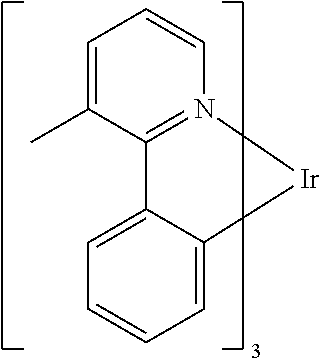 |
US20060240279 |
| Cross-linkable compounds |
 |
US20080220265 |
| Polythiophene based polymers and copolymers |
 |
WO 2011075644 EP2350216 |
| Hole transporting materials |
| Triarylamines (e.g., TPD, □-NPD) |
 |
Appl. Phys. Lett. 51, 913 (1987) |
 |
U.S. Pat. No. 5,061,569 | |
 |
EP650955 | |
 |
J. Mater. Chem. 3, 319 (1993) | |
 |
Appl. Phys. Lett. 90, 183503 (2007) | |
 |
Appl. Phys. Lett. 90, 183503 (2007) | |
| Triarylamine on spirofluorene core |
 |
Synth. Met. 91, 209 (1997) |
| Arylamine carbazole compounds |
 |
Adv. Mater. 6, 677 (1994), US20080124572 |
| Triarylamine with (di)benzothiophene/(di)benzo- furan |
 |
US20070278938, US20080106190 US20110163302 |
| Indolocarbazoles |
 |
Synth. Met. 111, 421 (2000) |
| Isoindole compounds |
 |
Chem. Mater. 15, 3148 (2003) |
| Metal carbene complexes |
 |
US20080018221 |
| Phosphorescent OLED host materials |
| Red hosts |
| Arylcarbazoles |
 |
Appl. Phys. Lett. 78, 1622 (2001) |
| Metal 8-hydroxyquinolates (e.g., Alq3, BAlq) |
 |
Nature 395, 151 (1998) |
 |
US20060202194 | |
 |
WO2005014551 | |
 |
WO2006072002 | |
| Metal phenoxybenzothiazole compounds |
 |
Appl. Phys. Lett. 90, 123509 (2007) |
| Conjugated oligomers and polymers (e.g., polyfluorene) |
 |
Org. Electron. 1, 15 (2000) |
| Aromatic fused rings |
 |
WO2009066779, WO2009066778, WO2009063833, US20090045731, US20090045730, WO2009008311, US20090008605, US20090009065 |
| Zinc complexes |
 |
WO2010056066 |
| Chrysene based compounds |
 |
WO2011086863 |
| Green hosts |
| Arylcarbazoles |
 |
Appl. Phys. Lett. 78, 1622 (2001) |
 |
US20030175553 | |
 |
WO2001039234 | |
| Aryltriphenylene compounds |
 |
US20060280965 |
 |
US20060280965 | |
 |
WO2009021126 | |
| Poly-fused heteroaryl compounds |
 |
US20090309488 US20090302743 US20100012931 |
| Donor acceptor type molecules |
 |
WO2008056746 |
 |
WO2010107244 | |
| Aza-carbazole/DBT/DBF |
 |
JP2008074939 |
 |
US20100187984 | |
| Polymers (e.g., PVK) |
 |
Appl. Phys. Lett. 77, 2280 (2000) |
| Spirofluorene compounds |
 |
WO2004093207 |
| Metal phenoxybenzooxazole compounds |
 |
WO2005089025 |
 |
WO2006132173 | |
 |
JP200511610 | |
| Spirofluorene-carbazole compounds |
 |
JP2007254297 |
 |
JP2007254297 | |
| Indolocarbazoles |
 |
WO2007063796 |
 |
WO2007063754 | |
| 5-membered ring electron deficient heterocycles (e.g., triazole, oxadiazole) |
 |
J. Appl. Phys. 90, 5048 (2001) |
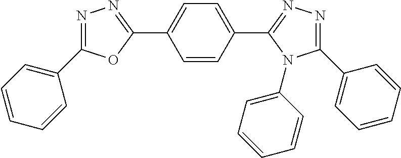 |
WO2004107822 | |
| Tetraphenylene complexes |
 |
US20050112407 |
| Metal phenoxypyridine compounds |
 |
WO2005030900 |
| Metal coordination complexes (e.g., Zn, Al with N{circumflex over ( )}N ligands) |
 |
US20040137268, US20040137267 |
| Blue hosts |
| Arylcarbazoles |
 |
Appl. Phys. Lett, 82, 2422 (2003) |
 |
US20070190359 | |
| Dibenzothiophene/Dibenzofu- ran-carbazole compounds |
 |
WO2006114966, US20090167162 |
 |
US20090167162 | |
 |
WO2009086028 | |
 |
US20090030202, US20090017330 | |
 |
US20100084966 | |
| Silicon aryl compounds |
 |
US20050238919 |
 |
WO2009003898 | |
| Silicon/Germanium aryl compounds |
 |
EP2034538A |
| Aryl benzoyl ester |
 |
WO2006100298 |
| Carbazole linked by non- conjugated groups |
 |
US20040115476 |
| Aza-carbazoles |
 |
US20060121308 |
| High triplet metal organometallic complex |
 |
U.S. Pat. No. 7,154,114 |
| Phosphorescent dopants |
| Red dopants |
| Heavy metal porphyrins (e.g., PtOEP) |
 |
Nature 395, 151 (1998) |
| Iridium(III) organometallic complexes |
 |
Appl. Phys. Lett. 78, 1622 (2001) |
 |
US20030072964 | |
 |
US20030072964 | |
 |
US20060202194 | |
 |
US20060202194 | |
 |
US20070087321 | |
 |
US20080261076 US20100090591 | |
 |
US20070087321 | |
 |
Adv. Mater. 19, 739 (2007) | |
 |
WO2009100991 | |
 |
WO2008101842 | |
 |
U.S. Pat. No. 7,232,618 | |
| Platinum(II) organometallic complexes |
 |
WO2003040257 |
 |
US20070103060 | |
| Osmium(III) complexes |
 |
Chem. Mater. 17, 3532 (2005) |
| Ruthenium(II) complexes |
 |
Adv. Mater. 17, 1059 (2005) |
| Rhenium (I), (II), and (III) complexes |
 |
US20050244673 |
| Green dopants |
| Iridium(III) organometallic complexes |
 |
Inorg. Chem. 40, 1704 (2001) |
 |
US20020034656 | |
 |
U.S. Pat. No. 7,332,232 | |
 |
US20090108737 | |
 |
WO2010028151 | |
 |
EP1841834B | |
 |
US20060127696 | |
 |
US20090039776 | |
 |
U.S. Pat. No. 6,921,915 | |
 |
US20100244004 | |
 |
U.S. Pat. No. 6,687,266 | |
 |
Chem. Mater. 16, 2480 (2004) | |
 |
US20070190359 | |
 |
US 20060008670 JP2007123392 | |
 |
WO2010086089, WO2011044988 | |
 |
Adv. Mater. 16, 2003 (2004) | |
 |
Angew. Chem. Int. Ed. 2006, 45, 7800 | |
 |
WO2009050290 | |
 |
US20090165846 | |
 |
US20080015355 | |
 |
US20010015432 | |
 |
US20100295032 | |
| Monomer for polymeric metal organometallic compounds |
 |
U.S. Pat. No. 7,250,226, U.S. Pat. No. 7,396,598 |
| Pt(II) organometallic complexes, including polydentated ligands |
 |
Appl. Phys. Lett. 86, 153505 (2005) |
 |
Appl. Phys. Lett. 86, 153505 (2005) | |
 |
Chem. Lett. 34, 592 (2005) | |
 |
WO2002015645 | |
 |
US20060263635 | |
 |
US20060182992 US20070103060 | |
| Cu complexes |
 |
WO2009000673 |
 |
US20070111026 | |
| Gold complexes |
 |
Chem. Commun. 2906 (2005) |
| Rhenium(III) complexes |
 |
Inorg. Chem. 42, 1248 (2003) |
| Osmium(II) complexes |
 |
U.S. Pat. No. 7,279,704 |
| Deuterated organometallic complexes |
 |
US20030138657 |
| Organometallic complexes with two or more metal centers |
 |
US20030152802 |
 |
U.S. Pat. No. 7,090,928 | |
| Blue dopants |
| Iridium(III) organometallic complexes |
 |
WO2002002714 |
 |
WO2006009024 | |
 |
US20060251923 US20110057559 US20110204333 | |
 |
U.S. Pat. No. 7,393,599, WO2006056418, US20050260441, WO2005019373 | |
 |
U.S. Pat. No. 7,534,505 | |
 |
WO2011051404 | |
 |
U.S. Pat. No. 7,445,855 | |
 |
US20070190359, US20080297033 US20100148663 | |
 |
U.S. Pat. No. 7,338,722 | |
 |
US20020134984 | |
 |
Angew. Chem. Int. Ed. 47, 4542 (2008) | |
 |
Chem. Mater. 18, 5119 (2006) | |
 |
Inorg. Chem. 46, 4308 (2007) | |
 |
WO2005123873 | |
 |
WO2005123873 | |
 |
WO2007004380 | |
 |
WO2006082742 | |
| Osmium(II) complexes |
 |
U.S. Pat. No. 7,279,704 |
 |
Organometallics 23, 3745 (2004) | |
| Gold complexes |
|
Appl. Phys. Lett.74,1361 (1999) |
| Platinum(II) complexes |
 |
WO2006098120, WO2006103874 |
| Pt tetradentate complexes with at least one metal- carbene bond |
 |
U.S. Pat. No. 7,655,323 |
| Exciton/hole blocking layer materials |
| Bathocuprine compounds (e.g., BCP, BPhen) |
 |
Appl. Phys. Lett. 75, 4 (1999) |
 |
Appl. Phys. Lett. 79, 449 (2001) | |
| Metal 8-hydroxyquinolates (e.g., BAlq) |
 |
Appl. Phys. Lett. 81, 162 (2002) |
| 5-membered ring electron deficient heterocycles such as triazole, oxadiazole, imidazole, benzoimidazole |
 |
Appl. Phys. Lett. 81, 162 (2002) |
| Triphenylene compounds |
 |
US20050025993 |
| Fluorinated aromatic compounds |
 |
Appl. Phys. Lett. 79, 156 (2001) |
| Phenothiazine-S-oxide |
 |
WO2008132085 |
| Silylated five-membered nitrogen, oxygen, sulfur or phosphorus dibenzoheterocycles |
 |
WO2010079051 |
| Aza-carbazoles |
 |
US20060121308 |
| Electron transporting materials |
| Anthracene-benzoimidazole compounds |
 |
WO2003060956 |
 |
US20090179554 | |
| Aza triphenylene derivatives |
 |
US20090115316 |
| Anthracene-benzothiazole compounds |
 |
Appl. Phys. Lett. 89, 063504 (2006) |
| Metal 8-hydroxyquinolates (e.g., Alq3, Zrq4) |
 |
Appl. Phys. Lett. 51, 913 (1987) U.S. Pat. No. 7,230,107 |
| Metal hydroxybenoquinolates |
 |
Chem. Lett. 5, 905 (1993) |
| Bathocuprine compounds such as BCP, BPhen, etc. |
 |
Appl. Phys. Lett. 91, 263503 (2007) |
 |
Appl. Phys. Lett. 79, 449 (2001) | |
| 5-membered ring electron deficient heterocycles (e.g., triazole, oxadiazole, imidazole, benzoimidazole) |
 |
Appl. Phys. Lett. 74, 865 (1999) |
 |
Appl. Phys. Lett. 55, 1489 (1989) | |
 |
Jpn. J. Apply. Phys. 32, L917 (1993) | |
| Silole compounds |
 |
Org. Electron. 4, 113 (2003) |
| Arylborane compounds |
 |
J. Am. Chem. Soc. 120, 9714 (1998) |
| Fluorinated aromatic compounds |
 |
J. Am. Chem. Soc. 122, 1832 (2000) |
| Fullerene (e.g., C60) |
 |
US20090101870 |
| Triazine complexes |
 |
US20040036077 |
| Zn (N{circumflex over ( )}N) complexes |
 |
U.S. Pat. No. 6,528,187 |
Claims (17)


Priority Applications (1)
| Application Number | Priority Date | Filing Date | Title |
|---|---|---|---|
| US16/897,694 US11641774B2 (en) | 2014-09-29 | 2020-06-10 | Organic electroluminescent materials and devices |
Applications Claiming Priority (3)
| Application Number | Priority Date | Filing Date | Title |
|---|---|---|---|
| US201462056940P | 2014-09-29 | 2014-09-29 | |
| US14/863,768 US10749113B2 (en) | 2014-09-29 | 2015-09-24 | Organic electroluminescent materials and devices |
| US16/897,694 US11641774B2 (en) | 2014-09-29 | 2020-06-10 | Organic electroluminescent materials and devices |
Related Parent Applications (1)
| Application Number | Title | Priority Date | Filing Date |
|---|---|---|---|
| US14/863,768 Continuation US10749113B2 (en) | 2014-09-29 | 2015-09-24 | Organic electroluminescent materials and devices |
Publications (2)
| Publication Number | Publication Date |
|---|---|
| US20200303652A1 US20200303652A1 (en) | 2020-09-24 |
| US11641774B2 true US11641774B2 (en) | 2023-05-02 |
Family
ID=55585386
Family Applications (2)
| Application Number | Title | Priority Date | Filing Date |
|---|---|---|---|
| US14/863,768 Active 2036-11-02 US10749113B2 (en) | 2014-09-29 | 2015-09-24 | Organic electroluminescent materials and devices |
| US16/897,694 Active 2036-09-12 US11641774B2 (en) | 2014-09-29 | 2020-06-10 | Organic electroluminescent materials and devices |
Family Applications Before (1)
| Application Number | Title | Priority Date | Filing Date |
|---|---|---|---|
| US14/863,768 Active 2036-11-02 US10749113B2 (en) | 2014-09-29 | 2015-09-24 | Organic electroluminescent materials and devices |
Country Status (1)
| Country | Link |
|---|---|
| US (2) | US10749113B2 (en) |
Families Citing this family (67)
| Publication number | Priority date | Publication date | Assignee | Title |
|---|---|---|---|---|
| CN102473857A (en) | 2010-01-15 | 2012-05-23 | 出光兴产株式会社 | Organic electroluminescent element |
| US9512355B2 (en) * | 2011-12-09 | 2016-12-06 | Universal Display Corporation | Organic light emitting materials |
| KR101542714B1 (en) * | 2014-04-04 | 2015-08-12 | 주식회사 엘지화학 | Hetero-cyclic compound and organic light emitting device comprising the same |
| KR101537500B1 (en) | 2014-04-04 | 2015-07-20 | 주식회사 엘지화학 | Organic light emitting diode |
| KR20150115622A (en) | 2014-04-04 | 2015-10-14 | 주식회사 엘지화학 | Hetero-cyclic compound and organic light emitting device comprising the same |
| WO2016084962A1 (en) * | 2014-11-28 | 2016-06-02 | 出光興産株式会社 | Compound, organic electroluminescence element material, organic electroluminescence element and electronic device |
| JP6754185B2 (en) * | 2015-12-10 | 2020-09-09 | コニカミノルタ株式会社 | Organic functional materials for organic electroluminescence devices, display devices, lighting devices and electronic devices |
| KR20170116500A (en) * | 2016-04-11 | 2017-10-19 | 주식회사 두산 | Organic light-emitting compound and organic electroluminescent device using the same |
| KR102044942B1 (en) * | 2016-05-02 | 2019-11-14 | 삼성에스디아이 주식회사 | Compound for organic optoelectric device and organic optoelectric device and display device |
| US11691983B2 (en) | 2016-06-22 | 2023-07-04 | Idemitsu Kosan Co., Ltd. | Specifically substituted benzofuro- and benzothienoquinolines for organic light emitting diodes |
| KR101849747B1 (en) * | 2016-07-20 | 2018-05-31 | 주식회사 엘지화학 | Novel hetero-cyclic compound and organic light emitting device comprising the same |
| WO2018043761A1 (en) * | 2016-09-05 | 2018-03-08 | Idemitsu Kosan Co.,Ltd. | Specifically substituted aza-dibenzofurans and aza-dibenzothiophenes for organic electronic devices |
| KR101939152B1 (en) * | 2016-09-12 | 2019-01-16 | (주)씨엠디엘 | Fluorenyl triazine derivative organic compound and organic electroluminescent device including the same |
| KR102041588B1 (en) | 2016-09-29 | 2019-11-06 | 삼성에스디아이 주식회사 | Compound for organic optoelectronic device, composition for organic optoelectronic device and organic optoelectronic device and display device |
| KR20180038834A (en) * | 2016-10-07 | 2018-04-17 | 삼성에스디아이 주식회사 | Composition for organic optoelectronic device and organic optoelectronic device and display device |
| KR101885899B1 (en) * | 2016-11-07 | 2018-08-06 | 주식회사 엘지화학 | Novel hetero-cyclic compound and organic light emitting device comprising the same |
| WO2018084423A2 (en) * | 2016-11-07 | 2018-05-11 | 주식회사 엘지화학 | Novel heterocyclic compound and organic light emitting element using same |
| KR101885898B1 (en) | 2016-11-16 | 2018-08-06 | 주식회사 엘지화학 | Organic light emitting device |
| KR101978453B1 (en) * | 2016-11-29 | 2019-05-14 | 주식회사 엘지화학 | Novel hetero-cyclic compound and organic light emitting device comprising the same |
| KR102078302B1 (en) * | 2016-11-29 | 2020-02-18 | 주식회사 엘지화학 | Organic light emitting device |
| CN109790461B (en) * | 2016-12-08 | 2022-08-12 | 广州华睿光电材料有限公司 | Mixture, composition and organic electronic device |
| JP7114596B2 (en) * | 2016-12-22 | 2022-08-08 | メルク パテント ゲーエムベーハー | A mixture containing at least two organic functional compounds |
| WO2018124697A1 (en) * | 2016-12-27 | 2018-07-05 | Rohm And Haas Electronic Materials Korea Ltd. | Organic electroluminescent compound and organic electroluminescent device comprising the same |
| KR102359412B1 (en) * | 2016-12-27 | 2022-02-09 | 롬엔드하스전자재료코리아유한회사 | Organic electroluminescent compound and organic electroluminescent device comprising the same |
| KR102017790B1 (en) * | 2017-04-13 | 2019-09-03 | 주식회사 엘지화학 | Novel hetero-cyclic compound and organic light emitting device comprising the same |
| KR101947747B1 (en) | 2018-05-04 | 2019-02-13 | 삼성에스디아이 주식회사 | Compound for organic optoelectronic device, composition for organic optoelectronic device and organic optoelectronic device and display device |
| KR102008897B1 (en) | 2017-06-22 | 2019-10-23 | 삼성에스디아이 주식회사 | Organic optoelectronic device and display device |
| US20190198772A1 (en) | 2017-06-22 | 2019-06-27 | Samsung Sdi Co., Ltd. | Compound for organic optoelectronic device, composition for organic optoelectronic device and organic optoelectronic device and display deivce |
| KR102101473B1 (en) | 2017-07-10 | 2020-04-16 | 주식회사 엘지화학 | Hetero-cyclic compound and organic light emitting device comprising the same |
| KR101982791B1 (en) | 2017-07-20 | 2019-05-27 | 주식회사 엘지화학 | Novel hetero-cyclic compound and organic light emitting device comprising the same |
| KR102155883B1 (en) * | 2017-07-31 | 2020-09-15 | 엘티소재주식회사 | Heterocyclic compound and organic light emitting device comprising the same |
| KR101856728B1 (en) * | 2017-08-10 | 2018-05-10 | 주식회사 엘지화학 | Organic light emitting device |
| CN109575083A (en) | 2017-09-29 | 2019-04-05 | 北京夏禾科技有限公司 | The luminous organic material of the assistant ligand containing naphthenic base |
| EP3466954A1 (en) | 2017-10-04 | 2019-04-10 | Idemitsu Kosan Co., Ltd. | Fused phenylquinazolines bridged with a heteroatom |
| CN109836421B (en) * | 2017-11-24 | 2021-09-10 | 北京鼎材科技有限公司 | A compound of general formula and its application |
| KR102134383B1 (en) | 2017-12-12 | 2020-07-15 | 주식회사 엘지화학 | Organic light emitting device |
| CN111247159A (en) * | 2017-12-14 | 2020-06-05 | 广州华睿光电材料有限公司 | Transition metal complex material and application thereof in electronic device |
| KR102163072B1 (en) * | 2017-12-27 | 2020-10-07 | 주식회사 엘지화학 | Organic light emitting device |
| KR102171533B1 (en) * | 2017-12-27 | 2020-10-29 | 삼성에스디아이 주식회사 | Composition and organic optoelectronic device and display device |
| WO2019132545A1 (en) * | 2017-12-27 | 2019-07-04 | 주식회사 엘지화학 | Organic light-emitting device |
| US11370782B2 (en) | 2018-03-06 | 2022-06-28 | Lg Chem, Ltd. | Compound and organic light emitting device comprising the same |
| KR102262471B1 (en) * | 2018-04-02 | 2021-06-09 | 삼성에스디아이 주식회사 | Composition and organic optoelectronic device and display device |
| KR102147908B1 (en) * | 2018-05-11 | 2020-08-25 | 주식회사 엘지화학 | Novel hetero-cyclic compound and organic light emitting device comprising the same |
| WO2019221486A1 (en) * | 2018-05-14 | 2019-11-21 | 주식회사 엘지화학 | Compound and organic light emitting device comprising same |
| US20220332724A1 (en) | 2018-05-30 | 2022-10-20 | Merck Patent Gmbh | Composition for organic electronic devices |
| US11767315B2 (en) * | 2018-06-14 | 2023-09-26 | Lg Chem, Ltd. | Heterocyclic compound and organic light-emitting device including same |
| WO2020013572A1 (en) * | 2018-07-09 | 2020-01-16 | 주식회사 엘지화학 | Compound and organic light emitting diode comprising same |
| US11753425B2 (en) * | 2018-07-11 | 2023-09-12 | Universal Display Corporation | Organic electroluminescent materials and devices |
| EP3604477A1 (en) | 2018-07-30 | 2020-02-05 | Idemitsu Kosan Co., Ltd. | Polycyclic compound, organic electroluminescence device, and electronic device |
| KR102199112B1 (en) | 2018-07-31 | 2021-01-06 | 솔루스첨단소재 주식회사 | Organic compound and organic electroluminescent device using the same |
| EP3608319A1 (en) | 2018-08-07 | 2020-02-12 | Idemitsu Kosan Co., Ltd. | Condensed aza cycles as organic light emitting device and materials for use in same |
| US11515482B2 (en) * | 2018-10-23 | 2022-11-29 | Universal Display Corporation | Deep HOMO (highest occupied molecular orbital) emitter device structures |
| KR102336599B1 (en) | 2018-11-16 | 2021-12-07 | 주식회사 엘지화학 | Novel compound and organic light emitting device comprising the same |
| EP3674295A1 (en) | 2018-12-28 | 2020-07-01 | Samsung Electronics Co., Ltd. | Heterocyclic compound, composition including heterocyclic compound, and organic light-emitting device including heterocyclic compound |
| US11542252B2 (en) | 2018-12-28 | 2023-01-03 | Samsung Electronics Co., Ltd. | Heterocyclic compound, composition including the same, and organic light-emitting device including the heterocyclic compound |
| US11925106B2 (en) | 2018-12-28 | 2024-03-05 | Samsung Electronics Co., Ltd. | Condensed cyclic compound, composition including the same, and organic light-emitting device including the condensed cyclic compound |
| CN111620853B (en) | 2019-02-28 | 2023-07-28 | 北京夏禾科技有限公司 | Organic electroluminescent material and device thereof |
| CN109912610B (en) * | 2019-04-04 | 2020-06-23 | 石家庄诚志永华显示材料有限公司 | Organic compound and application thereof in preparation of organic electroluminescent element |
| CN111909214B (en) | 2019-05-09 | 2024-03-29 | 北京夏禾科技有限公司 | Organic luminescent material containing 3-deuterium substituted isoquinoline ligand |
| CN111909212B (en) | 2019-05-09 | 2023-12-26 | 北京夏禾科技有限公司 | Organic luminescent material containing 6-silicon-based substituted isoquinoline ligand |
| CN111909213B (en) | 2019-05-09 | 2024-02-27 | 北京夏禾科技有限公司 | Metal complex containing three different ligands |
| KR20210043993A (en) * | 2019-10-14 | 2021-04-22 | 솔루스첨단소재 주식회사 | Organic light-emitting compound and organic electroluminescent device comprising the same |
| CN110964009B (en) * | 2019-11-15 | 2021-08-17 | 北京绿人科技有限责任公司 | Compound containing phenanthroline structure, application thereof and organic electroluminescent device |
| KR20210066073A (en) * | 2019-11-27 | 2021-06-07 | 삼성디스플레이 주식회사 | Organometallic compound and organic light emitting device including the same |
| JP7443038B2 (en) | 2019-12-04 | 2024-03-05 | 三星電子株式会社 | Compounds, compositions, liquid compositions and organic electroluminescent devices |
| WO2023063163A1 (en) * | 2021-10-14 | 2023-04-20 | 出光興産株式会社 | Mixed powder for organic electroluminescent element, production method therefor, method for manufacturing organic electroluminescent element using said mixed powder, method for selecting compound in said mixed powder, and composition for vacuum deposition |
| CN114031645A (en) * | 2021-11-26 | 2022-02-11 | 北京燕化集联光电技术有限公司 | Organic luminescent material and application thereof |
Citations (160)
| Publication number | Priority date | Publication date | Assignee | Title |
|---|---|---|---|---|
| US4769292A (en) | 1987-03-02 | 1988-09-06 | Eastman Kodak Company | Electroluminescent device with modified thin film luminescent zone |
| US5061569A (en) | 1990-07-26 | 1991-10-29 | Eastman Kodak Company | Electroluminescent device with organic electroluminescent medium |
| US5247190A (en) | 1989-04-20 | 1993-09-21 | Cambridge Research And Innovation Limited | Electroluminescent devices |
| EP0650955A1 (en) | 1993-11-01 | 1995-05-03 | Hodogaya Chemical Co., Ltd. | Amine compound and electro-luminescence device comprising same |
| US5703436A (en) | 1994-12-13 | 1997-12-30 | The Trustees Of Princeton University | Transparent contacts for organic devices |
| US5707745A (en) | 1994-12-13 | 1998-01-13 | The Trustees Of Princeton University | Multicolor organic light emitting devices |
| US5834893A (en) | 1996-12-23 | 1998-11-10 | The Trustees Of Princeton University | High efficiency organic light emitting devices with light directing structures |
| US5844363A (en) | 1997-01-23 | 1998-12-01 | The Trustees Of Princeton Univ. | Vacuum deposited, non-polymeric flexible organic light emitting devices |
| US5981092A (en) | 1996-03-25 | 1999-11-09 | Tdk Corporation | Organic El device |
| US6013982A (en) | 1996-12-23 | 2000-01-11 | The Trustees Of Princeton University | Multicolor display devices |
| US6087196A (en) | 1998-01-30 | 2000-07-11 | The Trustees Of Princeton University | Fabrication of organic semiconductor devices using ink jet printing |
| US6091195A (en) | 1997-02-03 | 2000-07-18 | The Trustees Of Princeton University | Displays having mesa pixel configuration |
| US6097147A (en) | 1998-09-14 | 2000-08-01 | The Trustees Of Princeton University | Structure for high efficiency electroluminescent device |
| WO2001039234A2 (en) | 1999-11-24 | 2001-05-31 | The Trustees Of Princeton University | Organic light emitting diode having a blue phosphorescent molecule as an emitter |
| US6294398B1 (en) | 1999-11-23 | 2001-09-25 | The Trustees Of Princeton University | Method for patterning devices |
| US6303238B1 (en) | 1997-12-01 | 2001-10-16 | The Trustees Of Princeton University | OLEDs doped with phosphorescent compounds |
| EP1156536A2 (en) | 2000-05-19 | 2001-11-21 | Eastman Kodak Company | Method of using predoped materials for making an organic light-emitting device |
| US6337102B1 (en) | 1997-11-17 | 2002-01-08 | The Trustees Of Princeton University | Low pressure vapor phase deposition of organic thin films |
| WO2002002714A2 (en) | 2000-06-30 | 2002-01-10 | E.I. Du Pont De Nemours And Company | Electroluminescent iridium compounds with fluorinated phenylpyridines, phenylpyrimidines, and phenylquinolines and devices made with such compounds |
| WO2002015654A1 (en) | 2000-08-04 | 2002-02-21 | Toray Engineering Co., Ltd. | Mounting method and mounting device |
| US20020034656A1 (en) | 1998-09-14 | 2002-03-21 | Thompson Mark E. | Organometallic complexes as phosphorescent emitters in organic LEDs |
| US20020134984A1 (en) | 2001-02-01 | 2002-09-26 | Fuji Photo Film Co., Ltd. | Transition metal complex and light-emitting device |
| US20020158242A1 (en) | 1999-12-31 | 2002-10-31 | Se-Hwan Son | Electronic device comprising organic compound having p-type semiconducting characteristics |
| US6528187B1 (en) | 1998-09-08 | 2003-03-04 | Fuji Photo Film Co., Ltd. | Material for luminescence element and luminescence element using the same |
| WO2003040257A1 (en) | 2001-11-07 | 2003-05-15 | E. I. Du Pont De Nemours And Company | Electroluminescent platinum compounds and devices made with such compounds |
| US20030138657A1 (en) | 2000-12-07 | 2003-07-24 | Canon Kabushiki Kaisha | Deuterated semi-conducting organic compounds used for opto-electronic devices |
| WO2003060956A2 (en) | 2002-01-18 | 2003-07-24 | Lg Chem, Ltd. | New material for transporting electrons and organic electroluminescent display using the same |
| US20030152802A1 (en) | 2001-06-19 | 2003-08-14 | Akira Tsuboyama | Metal coordination compound and organic liminescence device |
| US20030162053A1 (en) | 1996-06-25 | 2003-08-28 | Marks Tobin J. | Organic light - emitting diodes and methods for assembly and enhanced charge injection |
| US20030175553A1 (en) | 2001-12-28 | 2003-09-18 | Thompson Mark E. | White light emitting oleds from combined monomer and aggregate emission |
| US20030230980A1 (en) | 2002-06-18 | 2003-12-18 | Forrest Stephen R | Very low voltage, high efficiency phosphorescent oled in a p-i-n structure |
| JP2004022334A (en) | 2002-06-17 | 2004-01-22 | Konica Minolta Holdings Inc | Organic electroluminescence element and display device |
| US6687266B1 (en) | 2002-11-08 | 2004-02-03 | Universal Display Corporation | Organic light emitting materials and devices |
| US20040036077A1 (en) | 2002-08-22 | 2004-02-26 | Fuji Photo Film Co., Ltd. | Light emitting element |
| US20040137267A1 (en) | 2002-12-27 | 2004-07-15 | Fuji Photo Film Co., Ltd. | Organic electroluminescent device |
| US20040137268A1 (en) | 2002-12-27 | 2004-07-15 | Fuji Photo Film Co., Ltd. | Organic electroluminescent device |
| WO2004070787A2 (en) | 2003-02-03 | 2004-08-19 | The Regents Of The University Of California | Method for making multifunctional organic thin films |
| US20040174116A1 (en) | 2001-08-20 | 2004-09-09 | Lu Min-Hao Michael | Transparent electrodes |
| WO2004093207A2 (en) | 2003-04-15 | 2004-10-28 | Covion Organic Semiconductors Gmbh | Mixtures of matrix materials and organic semiconductors capable of emission, use of the same and electronic components containing said mixtures |
| US6821643B1 (en) | 2000-01-21 | 2004-11-23 | Xerox Corporation | Electroluminescent (EL) devices |
| WO2004107822A1 (en) | 2003-05-29 | 2004-12-09 | Nippon Steel Chemical Co., Ltd. | Organic electroluminescent element |
| US6835469B2 (en) | 2001-10-17 | 2004-12-28 | The University Of Southern California | Phosphorescent compounds and devices comprising the same |
| JP2005011610A (en) | 2003-06-18 | 2005-01-13 | Nippon Steel Chem Co Ltd | Organic electroluminescent element |
| US20050025993A1 (en) | 2003-07-25 | 2005-02-03 | Thompson Mark E. | Materials and structures for enhancing the performance of organic light emitting devices |
| WO2005014551A1 (en) | 2003-08-07 | 2005-02-17 | Nippon Steel Chemical Co., Ltd. | Aluminum chelate compelx for organic el material |
| WO2005019373A2 (en) | 2003-08-19 | 2005-03-03 | Basf Aktiengesellschaft | Transition metal complexes comprising carbene ligands serving as emitters for organic light-emitting diodes (oled's) |
| WO2005030900A1 (en) | 2003-09-25 | 2005-04-07 | Nippon Steel Chemical Co., Ltd. | Organic electroluminescent device |
| US20050112407A1 (en) | 2003-11-21 | 2005-05-26 | Fuji Photo Film Co., Ltd. | Organic electroluminescent device |
| US6921915B2 (en) | 2001-03-08 | 2005-07-26 | Canon Kabushiki Kaisha | Metal coordination compound, luminescence device and display apparatus |
| WO2005089025A1 (en) | 2004-03-15 | 2005-09-22 | Nippon Steel Chemical Co., Ltd. | Organic electroluminescent device |
| US20050238919A1 (en) | 2004-04-23 | 2005-10-27 | Fuji Photo Film Co., Ltd. | Organic electroluminescent device |
| US20050244673A1 (en) | 2002-08-27 | 2005-11-03 | Fujitsu Limited | Organometallic complex, organic EL element and organic EL display |
| US20050260441A1 (en) | 2004-05-18 | 2005-11-24 | Thompson Mark E | Luminescent compounds with carbene ligands |
| US20050260449A1 (en) | 2004-05-18 | 2005-11-24 | Robert Walters | Complexes with tridentate ligands |
| WO2005123873A1 (en) | 2004-06-17 | 2005-12-29 | Konica Minolta Holdings, Inc. | Organic electroluminescent device material, organic electroluminescent device, display and illuminating device |
| US20060008670A1 (en) | 2004-07-06 | 2006-01-12 | Chun Lin | Organic light emitting materials and devices |
| WO2006009024A1 (en) | 2004-07-23 | 2006-01-26 | Konica Minolta Holdings, Inc. | Organic electroluminescent device, display and illuminating device |
| WO2006056418A2 (en) | 2004-11-25 | 2006-06-01 | Basf Aktiengesellschaft | Use of transition metal carbene complexes in organic light-emitting diodes (oleds) |
| WO2006072002A2 (en) | 2004-12-30 | 2006-07-06 | E.I. Dupont De Nemours And Company | Organometallic complexes |
| US7087321B2 (en) | 2003-04-22 | 2006-08-08 | Universal Display Corporation | Organic light emitting devices having reduced pixel shrinkage |
| WO2006082742A1 (en) | 2005-02-04 | 2006-08-10 | Konica Minolta Holdings, Inc. | Organic electroluminescent device material, organic electroluminescent device, display and illuminating device |
| US7090928B2 (en) | 2003-04-01 | 2006-08-15 | The University Of Southern California | Binuclear compounds |
| US20060202194A1 (en) | 2005-03-08 | 2006-09-14 | Jeong Hyun C | Red phosphorescene compounds and organic electroluminescence device using the same |
| WO2006098120A1 (en) | 2005-03-16 | 2006-09-21 | Konica Minolta Holdings, Inc. | Organic electroluminescent device material and organic electroluminescent device |
| WO2006100298A1 (en) | 2005-03-24 | 2006-09-28 | Basf Aktiengesellschaft | Use of compounds containing aromatic or heteroaromatic rings linked via carbonyl group-containing groups, for use as matrix materials in organic light-emitting diodes |
| WO2006103874A1 (en) | 2005-03-29 | 2006-10-05 | Konica Minolta Holdings, Inc. | Organic electroluminescent device material, organic electroluminescent device, display and illuminating device |
| US20060240279A1 (en) | 2005-04-21 | 2006-10-26 | Vadim Adamovich | Non-blocked phosphorescent OLEDs |
| WO2006114966A1 (en) | 2005-04-18 | 2006-11-02 | Konica Minolta Holdings, Inc. | Organic electroluminescent device, display and illuminating device |
| US20060251923A1 (en) | 2005-05-06 | 2006-11-09 | Chun Lin | Stability OLED materials and devices |
| EP1725079A1 (en) | 2004-03-11 | 2006-11-22 | Mitsubishi Chemical Corporation | Composition for charge-transporting film and ion compound, charge-transporting film and organic electroluminescent device using same, and method for manufacturing organic electroluminescent device and method for producing charge-transporting film |
| US20060263635A1 (en) | 2005-05-06 | 2006-11-23 | Fuji Photo Film Co., Ltd. | Organic electroluminescent device |
| WO2006132173A1 (en) | 2005-06-07 | 2006-12-14 | Nippon Steel Chemical Co., Ltd. | Organic metal complex and organic electroluminescent device using same |
| US20060280965A1 (en) | 2005-05-31 | 2006-12-14 | Raymond Kwong | Triphenylene hosts in phosphorescent light emitting diodes |
| US7154114B2 (en) | 2004-05-18 | 2006-12-26 | Universal Display Corporation | Cyclometallated iridium carbene complexes for use as hosts |
| WO2007002683A2 (en) | 2005-06-27 | 2007-01-04 | E. I. Du Pont De Nemours And Company | Electrically conductive polymer compositions |
| WO2007004380A1 (en) | 2005-07-01 | 2007-01-11 | Konica Minolta Holdings, Inc. | Organic electroluminescent element material, organic electroluminescent element, display device, and lighting equipment |
| JP2007123392A (en) | 2005-10-26 | 2007-05-17 | Konica Minolta Holdings Inc | Organic electroluminescence device, display device and lighting device |
| WO2007063796A1 (en) | 2005-12-01 | 2007-06-07 | Nippon Steel Chemical Co., Ltd. | Organic electroluminescent device |
| WO2007063754A1 (en) | 2005-12-01 | 2007-06-07 | Nippon Steel Chemical Co., Ltd. | Compound for organic electroluminescent element and organic electroluminescent element |
| US7250226B2 (en) | 2001-08-31 | 2007-07-31 | Nippon Hoso Kyokai | Phosphorescent compound, a phosphorescent composition and an organic light-emitting device |
| US7252859B2 (en) | 2004-11-19 | 2007-08-07 | Eastman Kodak Company | Organic materials for an evaporation source |
| US20070190359A1 (en) | 2006-02-10 | 2007-08-16 | Knowles David B | Metal complexes of cyclometallated imidazo[1,2-ƒ]phenanthridine and diimidazo[1,2-a:1',2'-c]quinazoline ligands and isoelectronic and benzannulated analogs thereof |
| JP2007254297A (en) | 2006-03-20 | 2007-10-04 | Nippon Steel Chem Co Ltd | Compound of light-emitting layer and organic electroluminescent device |
| US20070249147A1 (en) | 2006-02-06 | 2007-10-25 | Fujifilm Corporation | Process and system for laser annealing and laser-annealed semiconductor film |
| US20070278938A1 (en) | 2006-04-26 | 2007-12-06 | Idemitsu Kosan Co., Ltd. | Aromatic amine derivative and electroluminescence device using the same |
| US20080015355A1 (en) | 2004-06-28 | 2008-01-17 | Thomas Schafer | Electroluminescent Metal Complexes With Triazoles And Benzotriazoles |
| US7332232B2 (en) | 2004-02-03 | 2008-02-19 | Universal Display Corporation | OLEDs utilizing multidentate ligand systems |
| US7338722B2 (en) | 2003-03-24 | 2008-03-04 | The University Of Southern California | Phenyl and fluorenyl substituted phenyl-pyrazole complexes of Ir |
| JP2008074939A (en) | 2006-09-21 | 2008-04-03 | Konica Minolta Holdings Inc | Organic electroluminescence element material, organic electroluminescence element, display device and illumination device |
| US20080106190A1 (en) | 2006-08-23 | 2008-05-08 | Idemitsu Kosan Co., Ltd. | Aromatic amine derivatives and organic electroluminescent device using same |
| WO2008056746A1 (en) | 2006-11-09 | 2008-05-15 | Nippon Steel Chemical Co., Ltd. | Compound for organic electroluminescent device and organic electroluminescent device |
| US20080124572A1 (en) | 2006-11-24 | 2008-05-29 | Idemitsu Kosan Co., Ltd. | Aromatic amine derivative and organic electroluminescence device using the same |
| US7393599B2 (en) | 2004-05-18 | 2008-07-01 | The University Of Southern California | Luminescent compounds with carbene ligands |
| US7396598B2 (en) | 2001-06-20 | 2008-07-08 | Showa Denko K.K. | Light emitting material and organic light-emitting device |
| WO2008101842A1 (en) | 2007-02-23 | 2008-08-28 | Basf Se | Electroluminescent metal complexes with benzotriazoles |
| US20080220265A1 (en) | 2006-12-08 | 2008-09-11 | Universal Display Corporation | Cross-linkable Iridium Complexes and Organic Light-Emitting Devices Using the Same |
| US7431968B1 (en) | 2001-09-04 | 2008-10-07 | The Trustees Of Princeton University | Process and apparatus for organic vapor jet deposition |
| US7445855B2 (en) | 2004-05-18 | 2008-11-04 | The University Of Southern California | Cationic metal-carbene complexes |
| WO2008132085A1 (en) | 2007-04-26 | 2008-11-06 | Basf Se | Silanes containing phenothiazine-s-oxide or phenothiazine-s,s-dioxide groups and the use thereof in oleds |
| US20080297033A1 (en) | 2006-02-10 | 2008-12-04 | Knowles David B | Blue phosphorescent imidazophenanthridine materials |
| WO2009000673A2 (en) | 2007-06-22 | 2008-12-31 | Basf Se | Light emitting cu(i) complexes |
| US20090008605A1 (en) | 2007-07-07 | 2009-01-08 | Idemitsu Kosan Co., Ltd. | Naphthalene derivative, material for organic electroluminescence device, and organic electroluminescence device using the same |
| WO2009003898A1 (en) | 2007-07-05 | 2009-01-08 | Basf Se | Organic light-emitting diodes containing carbene transition metal complex emitters and at least one compound selected from disilylcarbazoles, disilyldibenzofurans, disilyldibenzothiophenes, disilyldibenzophospholes, disilyldibenzothiophene s-oxides and disilyldibenzothiophene s,s-dioxides |
| US20090009065A1 (en) | 2007-07-07 | 2009-01-08 | Idemitsu Kosan Co., Ltd. | Organic electroluminescence device and material for organic electroluminescence device |
| WO2009008311A1 (en) | 2007-07-07 | 2009-01-15 | Idemitsu Kosan Co., Ltd. | Chrysene derivative and organic electroluminescent device using the same |
| US20090017330A1 (en) | 2007-07-10 | 2009-01-15 | Idemitsu Kosan Co., Ltd. | Material for organic electroluminescence device and organic electroluminescence device utilizing the same |
| US20090030202A1 (en) | 2007-07-10 | 2009-01-29 | Idemitsu Kosan Co., Ltd. | Material for organic electroluminescent element and organic electroluminescent element employing the same |
| WO2009018009A1 (en) | 2007-07-27 | 2009-02-05 | E. I. Du Pont De Nemours And Company | Aqueous dispersions of electrically conducting polymers containing inorganic nanoparticles |
| WO2009021126A2 (en) | 2007-08-08 | 2009-02-12 | Universal Display Corporation | Benzo-fused thiophene or benzo-fused furan compounds comprising a triphenylene group |
| US20090039776A1 (en) | 2007-08-09 | 2009-02-12 | Canon Kabushiki Kaisha | Organometallic complex and organic light-emitting element using same |
| US20090045730A1 (en) | 2007-07-07 | 2009-02-19 | Idemitsu Kosan Co., Ltd. | Organic electroluminescence device and material for organic electroluminescence device |
| US20090045731A1 (en) | 2007-07-07 | 2009-02-19 | Idemitsu Kosan Co., Ltd. | Organic electroluminescence device and material for organic electroluminescence device |
| EP2034538A1 (en) | 2006-06-02 | 2009-03-11 | Idemitsu Kosan Co., Ltd. | Material for organic electroluminescence element, and organic electroluminescence element using the material |
| US20090101870A1 (en) | 2007-10-22 | 2009-04-23 | E. I. Du Pont De Nemours And Company | Electron transport bi-layers and devices made with such bi-layers |
| WO2009050290A1 (en) | 2007-10-17 | 2009-04-23 | Basf Se | Transition metal complexes having bridged carbene ligands and the use thereof in oleds |
| US20090108737A1 (en) | 2006-12-08 | 2009-04-30 | Raymond Kwong | Light-emitting organometallic complexes |
| US20090115316A1 (en) | 2007-11-02 | 2009-05-07 | Shiying Zheng | Organic electroluminescent device having an azatriphenylene derivative |
| US7534505B2 (en) | 2004-05-18 | 2009-05-19 | The University Of Southern California | Organometallic compounds for use in electroluminescent devices |
| WO2009063833A1 (en) | 2007-11-15 | 2009-05-22 | Idemitsu Kosan Co., Ltd. | Benzochrysene derivative and organic electroluminescent device using the same |
| WO2009062578A1 (en) | 2007-11-12 | 2009-05-22 | Merck Patent Gmbh | Organic electroluminescent devices comprising azomethine-metal complexes |
| WO2009066779A1 (en) | 2007-11-22 | 2009-05-28 | Idemitsu Kosan Co., Ltd. | Organic el element |
| WO2009066778A1 (en) | 2007-11-22 | 2009-05-28 | Idemitsu Kosan Co., Ltd. | Organic el element and solution containing organic el material |
| US20090165846A1 (en) | 2005-09-07 | 2009-07-02 | Universitaet Braunschweig | Triplet emitter having condensed five-membered rings |
| US20090167162A1 (en) | 2007-12-28 | 2009-07-02 | Universal Display Corporation | Dibenzothiophene-containing materials in phosphorescent light emitting diodes |
| WO2009086028A2 (en) | 2007-12-28 | 2009-07-09 | Universal Display Corporation | Carbazole-containing materials in phosphorescent light emitting diodes |
| US20090179554A1 (en) | 2006-05-11 | 2009-07-16 | Hitoshi Kuma | Organic electroluminescent device |
| WO2009100991A1 (en) | 2008-02-12 | 2009-08-20 | Basf Se | Electroluminescent metal complexes with dibenzo[f,h]quinoxalines |
| US20110037057A1 (en) | 2009-02-27 | 2011-02-17 | E.I. Du Pont De Nemours And Company | Deuterated compounds for electronic applications |
| JP2011063584A (en) | 2009-08-21 | 2011-03-31 | Tosoh Corp | Triazine derivative, method for producing the same and organic electroluminescent element comprising the same as constituent component |
| US20110260138A1 (en) | 2010-04-26 | 2011-10-27 | Universal Display Corporation | Bicarbzole containing compounds for oleds |
| WO2011136755A1 (en) | 2010-04-28 | 2011-11-03 | Universal Display Corporation | Depositing premixed materials |
| WO2012033061A1 (en) | 2010-09-08 | 2012-03-15 | 富士フイルム株式会社 | Organic electroluminescent element and charge transport material |
| US20120126208A1 (en) | 2010-11-22 | 2012-05-24 | Idemitsu Kosan Co., Ltd. | Organic electroluminescence device |
| KR20120078301A (en) | 2010-12-31 | 2012-07-10 | 제일모직주식회사 | Compound for organic photoelectric device and organic photoelectric device including the same |
| WO2012133644A1 (en) | 2011-03-31 | 2012-10-04 | 富士フイルム株式会社 | Organic electroluminescent element, light-emitting device using organic electroluminescent element, display device using organic electroluminescent element, lighting device using organic electroluminescent element, and compound for organic electroluminescent element |
| KR20120129733A (en) | 2011-05-20 | 2012-11-28 | (주)씨에스엘쏠라 | Organic light compound and organic light device using the same |
| CN102850329A (en) | 2012-08-28 | 2013-01-02 | 李崇 | Triazinyl derivative compound and its application in OLED (organic light emission diode) |
| WO2013032297A1 (en) | 2011-09-01 | 2013-03-07 | Rohm And Haas Electronic Materials Korea Ltd. | Benzocarbazole compounds and electroluminescent devices involving them |
| US20130264560A1 (en) | 2010-12-20 | 2013-10-10 | E I Du Pont De Nemours And Company | Triazine derivatives for electronic applications |
| WO2013191177A1 (en) | 2012-06-18 | 2013-12-27 | 東ソー株式会社 | Cyclic azine compound, method for producing same, and organic electroluminescent element containing same |
| US20140001456A1 (en) | 2011-11-22 | 2014-01-02 | Idemitsu Kosan Co., Ltd. | Aromatic heterocyclic derivative, material for organic eletroluminescent element, and organic electroluminescent element |
| US8679647B2 (en) | 2008-12-22 | 2014-03-25 | Merck Patent Gmbh | Organic electroluminescent device comprising triazine derivatives |
| WO2014104515A1 (en) | 2012-12-31 | 2014-07-03 | 제일모직 주식회사 | Compound for organic optoelectric device, organic light emitting diode comprising same, and display apparatus comprising organic light emitting diode |
| JP2014125449A (en) | 2012-12-26 | 2014-07-07 | Tosoh Corp | Method of manufacturing cyclic azine compound |
| US20140231769A1 (en) * | 2013-02-15 | 2014-08-21 | Idemitsu Kosan Co., Ltd. | Organic electroluminescence device and electronic device |
| US20140264292A1 (en) | 2013-03-14 | 2014-09-18 | Universal Display Corporation | Host compounds for phosphorescent oleds and devices thereof |
| US20140299192A1 (en) | 2012-07-13 | 2014-10-09 | Lg Chem, Ltd. | Heterocyclic compound and organic electronic element containing same |
| US20140312338A1 (en) | 2011-11-22 | 2014-10-23 | Idemitsu Kosan Co., Ltd. | Aromatic heterocyclic derivative, material for organic electroluminescent element, and organic electroluminescent element |
| US20150001524A1 (en) | 2007-06-23 | 2015-01-01 | Universal Display Corporation | Organic electroluminescent materials and devices |
| US20150014649A1 (en) | 2013-07-15 | 2015-01-15 | Universal Display Corporation | Organic Light Emitting Diode Materials |
| US20150025239A1 (en) | 2012-02-17 | 2015-01-22 | Hee-Choon Ahn | Novel organic electroluminescent compounds and organic electroluminescent device using the same |
| US20150053938A1 (en) | 2013-08-20 | 2015-02-26 | Universal Display Corporation | Organic electroluminescent materials and devices |
| US20150053939A1 (en) | 2013-08-20 | 2015-02-26 | Universal Display Corporation | Organic electroluminescent materials and devices |
| JP2015134743A (en) | 2013-06-28 | 2015-07-27 | 東ソー株式会社 | Cyclic azine compound, method for producing the same and organic electroluminescent element using the same |
| US20150214489A1 (en) | 2012-07-23 | 2015-07-30 | Merck Patent Gmbh | Materials for organic electroluminescent devices |
| WO2015111848A1 (en) | 2014-01-24 | 2015-07-30 | 삼성에스디아이 주식회사 | Organic compound, composition, organic optoelectronic device, and display device |
| US20150249221A1 (en) | 2014-03-01 | 2015-09-03 | Universal Display Corporation | Organic electroluminescent materials and devices |
| US20150266863A1 (en) | 2014-03-18 | 2015-09-24 | Universal Display Corporation | Organic electroluminescent materials and devices |
| US20160141505A1 (en) | 2013-10-11 | 2016-05-19 | Samsung Sdi Co., Ltd | Organic alloy for organic optoelectronic device, organic optoelectronic device, and display device |
| US20160149139A1 (en) | 2014-11-25 | 2016-05-26 | Universal Display Corporation | Organic electroluminescent materials and devices |
Family Cites Families (6)
| Publication number | Priority date | Publication date | Assignee | Title |
|---|---|---|---|---|
| WO2002015645A1 (en) | 2000-08-11 | 2002-02-21 | The Trustees Of Princeton University | Organometallic compounds and emission-shifting organic electrophosphorescence |
| US6878975B2 (en) | 2002-02-08 | 2005-04-12 | Agilent Technologies, Inc. | Polarization field enhanced tunnel structures |
| EP1643568A1 (en) | 2004-10-04 | 2006-04-05 | Novaled GmbH | Method of forming a layer of a doped semiconductor material and apparatus |
| WO2010027583A1 (en) * | 2008-09-03 | 2010-03-11 | Universal Display Corporation | Phosphorescent materials |
| US9067947B2 (en) * | 2009-01-16 | 2015-06-30 | Universal Display Corporation | Organic electroluminescent materials and devices |
| JP5770289B2 (en) * | 2010-08-20 | 2015-08-26 | ユニバーサル ディスプレイ コーポレイション | Bicarbazole compounds for OLED |
-
2015
- 2015-09-24 US US14/863,768 patent/US10749113B2/en active Active
-
2020
- 2020-06-10 US US16/897,694 patent/US11641774B2/en active Active
Patent Citations (167)
| Publication number | Priority date | Publication date | Assignee | Title |
|---|---|---|---|---|
| US4769292A (en) | 1987-03-02 | 1988-09-06 | Eastman Kodak Company | Electroluminescent device with modified thin film luminescent zone |
| US5247190A (en) | 1989-04-20 | 1993-09-21 | Cambridge Research And Innovation Limited | Electroluminescent devices |
| US5061569A (en) | 1990-07-26 | 1991-10-29 | Eastman Kodak Company | Electroluminescent device with organic electroluminescent medium |
| EP0650955A1 (en) | 1993-11-01 | 1995-05-03 | Hodogaya Chemical Co., Ltd. | Amine compound and electro-luminescence device comprising same |
| US5703436A (en) | 1994-12-13 | 1997-12-30 | The Trustees Of Princeton University | Transparent contacts for organic devices |
| US5707745A (en) | 1994-12-13 | 1998-01-13 | The Trustees Of Princeton University | Multicolor organic light emitting devices |
| US5981092A (en) | 1996-03-25 | 1999-11-09 | Tdk Corporation | Organic El device |
| US20030162053A1 (en) | 1996-06-25 | 2003-08-28 | Marks Tobin J. | Organic light - emitting diodes and methods for assembly and enhanced charge injection |
| US6013982A (en) | 1996-12-23 | 2000-01-11 | The Trustees Of Princeton University | Multicolor display devices |
| US5834893A (en) | 1996-12-23 | 1998-11-10 | The Trustees Of Princeton University | High efficiency organic light emitting devices with light directing structures |
| US5844363A (en) | 1997-01-23 | 1998-12-01 | The Trustees Of Princeton Univ. | Vacuum deposited, non-polymeric flexible organic light emitting devices |
| US6091195A (en) | 1997-02-03 | 2000-07-18 | The Trustees Of Princeton University | Displays having mesa pixel configuration |
| US6337102B1 (en) | 1997-11-17 | 2002-01-08 | The Trustees Of Princeton University | Low pressure vapor phase deposition of organic thin films |
| US6303238B1 (en) | 1997-12-01 | 2001-10-16 | The Trustees Of Princeton University | OLEDs doped with phosphorescent compounds |
| US6087196A (en) | 1998-01-30 | 2000-07-11 | The Trustees Of Princeton University | Fabrication of organic semiconductor devices using ink jet printing |
| US6528187B1 (en) | 1998-09-08 | 2003-03-04 | Fuji Photo Film Co., Ltd. | Material for luminescence element and luminescence element using the same |
| US6097147A (en) | 1998-09-14 | 2000-08-01 | The Trustees Of Princeton University | Structure for high efficiency electroluminescent device |
| US20020034656A1 (en) | 1998-09-14 | 2002-03-21 | Thompson Mark E. | Organometallic complexes as phosphorescent emitters in organic LEDs |
| US6294398B1 (en) | 1999-11-23 | 2001-09-25 | The Trustees Of Princeton University | Method for patterning devices |
| US6468819B1 (en) | 1999-11-23 | 2002-10-22 | The Trustees Of Princeton University | Method for patterning organic thin film devices using a die |
| WO2001039234A2 (en) | 1999-11-24 | 2001-05-31 | The Trustees Of Princeton University | Organic light emitting diode having a blue phosphorescent molecule as an emitter |
| US20020158242A1 (en) | 1999-12-31 | 2002-10-31 | Se-Hwan Son | Electronic device comprising organic compound having p-type semiconducting characteristics |
| US6821643B1 (en) | 2000-01-21 | 2004-11-23 | Xerox Corporation | Electroluminescent (EL) devices |
| EP1156536A2 (en) | 2000-05-19 | 2001-11-21 | Eastman Kodak Company | Method of using predoped materials for making an organic light-emitting device |
| US20040016907A1 (en) * | 2000-05-19 | 2004-01-29 | Eastman Kodak Company | Method of using predoped materials for making an organic light-emitting device |
| WO2002002714A2 (en) | 2000-06-30 | 2002-01-10 | E.I. Du Pont De Nemours And Company | Electroluminescent iridium compounds with fluorinated phenylpyridines, phenylpyrimidines, and phenylquinolines and devices made with such compounds |
| WO2002015654A1 (en) | 2000-08-04 | 2002-02-21 | Toray Engineering Co., Ltd. | Mounting method and mounting device |
| US20030138657A1 (en) | 2000-12-07 | 2003-07-24 | Canon Kabushiki Kaisha | Deuterated semi-conducting organic compounds used for opto-electronic devices |
| US20020134984A1 (en) | 2001-02-01 | 2002-09-26 | Fuji Photo Film Co., Ltd. | Transition metal complex and light-emitting device |
| US6921915B2 (en) | 2001-03-08 | 2005-07-26 | Canon Kabushiki Kaisha | Metal coordination compound, luminescence device and display apparatus |
| US20030152802A1 (en) | 2001-06-19 | 2003-08-14 | Akira Tsuboyama | Metal coordination compound and organic liminescence device |
| US7396598B2 (en) | 2001-06-20 | 2008-07-08 | Showa Denko K.K. | Light emitting material and organic light-emitting device |
| US20040174116A1 (en) | 2001-08-20 | 2004-09-09 | Lu Min-Hao Michael | Transparent electrodes |
| US7250226B2 (en) | 2001-08-31 | 2007-07-31 | Nippon Hoso Kyokai | Phosphorescent compound, a phosphorescent composition and an organic light-emitting device |
| US7431968B1 (en) | 2001-09-04 | 2008-10-07 | The Trustees Of Princeton University | Process and apparatus for organic vapor jet deposition |
| US6835469B2 (en) | 2001-10-17 | 2004-12-28 | The University Of Southern California | Phosphorescent compounds and devices comprising the same |
| WO2003040257A1 (en) | 2001-11-07 | 2003-05-15 | E. I. Du Pont De Nemours And Company | Electroluminescent platinum compounds and devices made with such compounds |
| US20030175553A1 (en) | 2001-12-28 | 2003-09-18 | Thompson Mark E. | White light emitting oleds from combined monomer and aggregate emission |
| WO2003060956A2 (en) | 2002-01-18 | 2003-07-24 | Lg Chem, Ltd. | New material for transporting electrons and organic electroluminescent display using the same |
| JP2004022334A (en) | 2002-06-17 | 2004-01-22 | Konica Minolta Holdings Inc | Organic electroluminescence element and display device |
| US20030230980A1 (en) | 2002-06-18 | 2003-12-18 | Forrest Stephen R | Very low voltage, high efficiency phosphorescent oled in a p-i-n structure |
| US20040036077A1 (en) | 2002-08-22 | 2004-02-26 | Fuji Photo Film Co., Ltd. | Light emitting element |
| US20050244673A1 (en) | 2002-08-27 | 2005-11-03 | Fujitsu Limited | Organometallic complex, organic EL element and organic EL display |
| US6687266B1 (en) | 2002-11-08 | 2004-02-03 | Universal Display Corporation | Organic light emitting materials and devices |
| US20040137268A1 (en) | 2002-12-27 | 2004-07-15 | Fuji Photo Film Co., Ltd. | Organic electroluminescent device |
| US20040137267A1 (en) | 2002-12-27 | 2004-07-15 | Fuji Photo Film Co., Ltd. | Organic electroluminescent device |
| US20060134317A1 (en) | 2003-02-03 | 2006-06-22 | Yang Yang | Method for making multifunctional organic thin films |
| WO2004070787A2 (en) | 2003-02-03 | 2004-08-19 | The Regents Of The University Of California | Method for making multifunctional organic thin films |
| US7338722B2 (en) | 2003-03-24 | 2008-03-04 | The University Of Southern California | Phenyl and fluorenyl substituted phenyl-pyrazole complexes of Ir |
| US7090928B2 (en) | 2003-04-01 | 2006-08-15 | The University Of Southern California | Binuclear compounds |
| WO2004093207A2 (en) | 2003-04-15 | 2004-10-28 | Covion Organic Semiconductors Gmbh | Mixtures of matrix materials and organic semiconductors capable of emission, use of the same and electronic components containing said mixtures |
| US7087321B2 (en) | 2003-04-22 | 2006-08-08 | Universal Display Corporation | Organic light emitting devices having reduced pixel shrinkage |
| WO2004107822A1 (en) | 2003-05-29 | 2004-12-09 | Nippon Steel Chemical Co., Ltd. | Organic electroluminescent element |
| JP2005011610A (en) | 2003-06-18 | 2005-01-13 | Nippon Steel Chem Co Ltd | Organic electroluminescent element |
| US20050025993A1 (en) | 2003-07-25 | 2005-02-03 | Thompson Mark E. | Materials and structures for enhancing the performance of organic light emitting devices |
| WO2005014551A1 (en) | 2003-08-07 | 2005-02-17 | Nippon Steel Chemical Co., Ltd. | Aluminum chelate compelx for organic el material |
| WO2005019373A2 (en) | 2003-08-19 | 2005-03-03 | Basf Aktiengesellschaft | Transition metal complexes comprising carbene ligands serving as emitters for organic light-emitting diodes (oled's) |
| WO2005030900A1 (en) | 2003-09-25 | 2005-04-07 | Nippon Steel Chemical Co., Ltd. | Organic electroluminescent device |
| US20050112407A1 (en) | 2003-11-21 | 2005-05-26 | Fuji Photo Film Co., Ltd. | Organic electroluminescent device |
| US7332232B2 (en) | 2004-02-03 | 2008-02-19 | Universal Display Corporation | OLEDs utilizing multidentate ligand systems |
| EP1725079A1 (en) | 2004-03-11 | 2006-11-22 | Mitsubishi Chemical Corporation | Composition for charge-transporting film and ion compound, charge-transporting film and organic electroluminescent device using same, and method for manufacturing organic electroluminescent device and method for producing charge-transporting film |
| WO2005089025A1 (en) | 2004-03-15 | 2005-09-22 | Nippon Steel Chemical Co., Ltd. | Organic electroluminescent device |
| US20050238919A1 (en) | 2004-04-23 | 2005-10-27 | Fuji Photo Film Co., Ltd. | Organic electroluminescent device |
| US7534505B2 (en) | 2004-05-18 | 2009-05-19 | The University Of Southern California | Organometallic compounds for use in electroluminescent devices |
| US7445855B2 (en) | 2004-05-18 | 2008-11-04 | The University Of Southern California | Cationic metal-carbene complexes |
| US7393599B2 (en) | 2004-05-18 | 2008-07-01 | The University Of Southern California | Luminescent compounds with carbene ligands |
| US7279704B2 (en) | 2004-05-18 | 2007-10-09 | The University Of Southern California | Complexes with tridentate ligands |
| US20050260449A1 (en) | 2004-05-18 | 2005-11-24 | Robert Walters | Complexes with tridentate ligands |
| US20050260441A1 (en) | 2004-05-18 | 2005-11-24 | Thompson Mark E | Luminescent compounds with carbene ligands |
| US7154114B2 (en) | 2004-05-18 | 2006-12-26 | Universal Display Corporation | Cyclometallated iridium carbene complexes for use as hosts |
| WO2005123873A1 (en) | 2004-06-17 | 2005-12-29 | Konica Minolta Holdings, Inc. | Organic electroluminescent device material, organic electroluminescent device, display and illuminating device |
| US20080015355A1 (en) | 2004-06-28 | 2008-01-17 | Thomas Schafer | Electroluminescent Metal Complexes With Triazoles And Benzotriazoles |
| US20060008670A1 (en) | 2004-07-06 | 2006-01-12 | Chun Lin | Organic light emitting materials and devices |
| WO2006009024A1 (en) | 2004-07-23 | 2006-01-26 | Konica Minolta Holdings, Inc. | Organic electroluminescent device, display and illuminating device |
| US7252859B2 (en) | 2004-11-19 | 2007-08-07 | Eastman Kodak Company | Organic materials for an evaporation source |
| WO2006056418A2 (en) | 2004-11-25 | 2006-06-01 | Basf Aktiengesellschaft | Use of transition metal carbene complexes in organic light-emitting diodes (oleds) |
| US20080018221A1 (en) | 2004-11-25 | 2008-01-24 | Basf Aktiengesellschaft | Use Of Transition Metal Carbene Complexes In Organic Light-Emitting Diodes (Oleds) |
| WO2006072002A2 (en) | 2004-12-30 | 2006-07-06 | E.I. Dupont De Nemours And Company | Organometallic complexes |
| WO2006082742A1 (en) | 2005-02-04 | 2006-08-10 | Konica Minolta Holdings, Inc. | Organic electroluminescent device material, organic electroluminescent device, display and illuminating device |
| US20060202194A1 (en) | 2005-03-08 | 2006-09-14 | Jeong Hyun C | Red phosphorescene compounds and organic electroluminescence device using the same |
| WO2006098120A1 (en) | 2005-03-16 | 2006-09-21 | Konica Minolta Holdings, Inc. | Organic electroluminescent device material and organic electroluminescent device |
| WO2006100298A1 (en) | 2005-03-24 | 2006-09-28 | Basf Aktiengesellschaft | Use of compounds containing aromatic or heteroaromatic rings linked via carbonyl group-containing groups, for use as matrix materials in organic light-emitting diodes |
| WO2006103874A1 (en) | 2005-03-29 | 2006-10-05 | Konica Minolta Holdings, Inc. | Organic electroluminescent device material, organic electroluminescent device, display and illuminating device |
| WO2006114966A1 (en) | 2005-04-18 | 2006-11-02 | Konica Minolta Holdings, Inc. | Organic electroluminescent device, display and illuminating device |
| US20060240279A1 (en) | 2005-04-21 | 2006-10-26 | Vadim Adamovich | Non-blocked phosphorescent OLEDs |
| US20060263635A1 (en) | 2005-05-06 | 2006-11-23 | Fuji Photo Film Co., Ltd. | Organic electroluminescent device |
| US20060251923A1 (en) | 2005-05-06 | 2006-11-09 | Chun Lin | Stability OLED materials and devices |
| US20060280965A1 (en) | 2005-05-31 | 2006-12-14 | Raymond Kwong | Triphenylene hosts in phosphorescent light emitting diodes |
| WO2006132173A1 (en) | 2005-06-07 | 2006-12-14 | Nippon Steel Chemical Co., Ltd. | Organic metal complex and organic electroluminescent device using same |
| WO2007002683A2 (en) | 2005-06-27 | 2007-01-04 | E. I. Du Pont De Nemours And Company | Electrically conductive polymer compositions |
| WO2007004380A1 (en) | 2005-07-01 | 2007-01-11 | Konica Minolta Holdings, Inc. | Organic electroluminescent element material, organic electroluminescent element, display device, and lighting equipment |
| US20090165846A1 (en) | 2005-09-07 | 2009-07-02 | Universitaet Braunschweig | Triplet emitter having condensed five-membered rings |
| JP2007123392A (en) | 2005-10-26 | 2007-05-17 | Konica Minolta Holdings Inc | Organic electroluminescence device, display device and lighting device |
| WO2007063754A1 (en) | 2005-12-01 | 2007-06-07 | Nippon Steel Chemical Co., Ltd. | Compound for organic electroluminescent element and organic electroluminescent element |
| WO2007063796A1 (en) | 2005-12-01 | 2007-06-07 | Nippon Steel Chemical Co., Ltd. | Organic electroluminescent device |
| US20070249147A1 (en) | 2006-02-06 | 2007-10-25 | Fujifilm Corporation | Process and system for laser annealing and laser-annealed semiconductor film |
| US20080297033A1 (en) | 2006-02-10 | 2008-12-04 | Knowles David B | Blue phosphorescent imidazophenanthridine materials |
| US20070190359A1 (en) | 2006-02-10 | 2007-08-16 | Knowles David B | Metal complexes of cyclometallated imidazo[1,2-ƒ]phenanthridine and diimidazo[1,2-a:1',2'-c]quinazoline ligands and isoelectronic and benzannulated analogs thereof |
| JP2007254297A (en) | 2006-03-20 | 2007-10-04 | Nippon Steel Chem Co Ltd | Compound of light-emitting layer and organic electroluminescent device |
| US20070278938A1 (en) | 2006-04-26 | 2007-12-06 | Idemitsu Kosan Co., Ltd. | Aromatic amine derivative and electroluminescence device using the same |
| US20090179554A1 (en) | 2006-05-11 | 2009-07-16 | Hitoshi Kuma | Organic electroluminescent device |
| EP2034538A1 (en) | 2006-06-02 | 2009-03-11 | Idemitsu Kosan Co., Ltd. | Material for organic electroluminescence element, and organic electroluminescence element using the material |
| US20080106190A1 (en) | 2006-08-23 | 2008-05-08 | Idemitsu Kosan Co., Ltd. | Aromatic amine derivatives and organic electroluminescent device using same |
| JP2008074939A (en) | 2006-09-21 | 2008-04-03 | Konica Minolta Holdings Inc | Organic electroluminescence element material, organic electroluminescence element, display device and illumination device |
| WO2008056746A1 (en) | 2006-11-09 | 2008-05-15 | Nippon Steel Chemical Co., Ltd. | Compound for organic electroluminescent device and organic electroluminescent device |
| US20080124572A1 (en) | 2006-11-24 | 2008-05-29 | Idemitsu Kosan Co., Ltd. | Aromatic amine derivative and organic electroluminescence device using the same |
| US20090108737A1 (en) | 2006-12-08 | 2009-04-30 | Raymond Kwong | Light-emitting organometallic complexes |
| US20080220265A1 (en) | 2006-12-08 | 2008-09-11 | Universal Display Corporation | Cross-linkable Iridium Complexes and Organic Light-Emitting Devices Using the Same |
| WO2008101842A1 (en) | 2007-02-23 | 2008-08-28 | Basf Se | Electroluminescent metal complexes with benzotriazoles |
| WO2008132085A1 (en) | 2007-04-26 | 2008-11-06 | Basf Se | Silanes containing phenothiazine-s-oxide or phenothiazine-s,s-dioxide groups and the use thereof in oleds |
| WO2009000673A2 (en) | 2007-06-22 | 2008-12-31 | Basf Se | Light emitting cu(i) complexes |
| US20150001524A1 (en) | 2007-06-23 | 2015-01-01 | Universal Display Corporation | Organic electroluminescent materials and devices |
| WO2009003898A1 (en) | 2007-07-05 | 2009-01-08 | Basf Se | Organic light-emitting diodes containing carbene transition metal complex emitters and at least one compound selected from disilylcarbazoles, disilyldibenzofurans, disilyldibenzothiophenes, disilyldibenzophospholes, disilyldibenzothiophene s-oxides and disilyldibenzothiophene s,s-dioxides |
| US20090008605A1 (en) | 2007-07-07 | 2009-01-08 | Idemitsu Kosan Co., Ltd. | Naphthalene derivative, material for organic electroluminescence device, and organic electroluminescence device using the same |
| US20090045730A1 (en) | 2007-07-07 | 2009-02-19 | Idemitsu Kosan Co., Ltd. | Organic electroluminescence device and material for organic electroluminescence device |
| US20090045731A1 (en) | 2007-07-07 | 2009-02-19 | Idemitsu Kosan Co., Ltd. | Organic electroluminescence device and material for organic electroluminescence device |
| US20090009065A1 (en) | 2007-07-07 | 2009-01-08 | Idemitsu Kosan Co., Ltd. | Organic electroluminescence device and material for organic electroluminescence device |
| WO2009008311A1 (en) | 2007-07-07 | 2009-01-15 | Idemitsu Kosan Co., Ltd. | Chrysene derivative and organic electroluminescent device using the same |
| US20090030202A1 (en) | 2007-07-10 | 2009-01-29 | Idemitsu Kosan Co., Ltd. | Material for organic electroluminescent element and organic electroluminescent element employing the same |
| US20090017330A1 (en) | 2007-07-10 | 2009-01-15 | Idemitsu Kosan Co., Ltd. | Material for organic electroluminescence device and organic electroluminescence device utilizing the same |
| WO2009018009A1 (en) | 2007-07-27 | 2009-02-05 | E. I. Du Pont De Nemours And Company | Aqueous dispersions of electrically conducting polymers containing inorganic nanoparticles |
| WO2009021126A2 (en) | 2007-08-08 | 2009-02-12 | Universal Display Corporation | Benzo-fused thiophene or benzo-fused furan compounds comprising a triphenylene group |
| US20090039776A1 (en) | 2007-08-09 | 2009-02-12 | Canon Kabushiki Kaisha | Organometallic complex and organic light-emitting element using same |
| WO2009050290A1 (en) | 2007-10-17 | 2009-04-23 | Basf Se | Transition metal complexes having bridged carbene ligands and the use thereof in oleds |
| US20090101870A1 (en) | 2007-10-22 | 2009-04-23 | E. I. Du Pont De Nemours And Company | Electron transport bi-layers and devices made with such bi-layers |
| US20090115316A1 (en) | 2007-11-02 | 2009-05-07 | Shiying Zheng | Organic electroluminescent device having an azatriphenylene derivative |
| WO2009062578A1 (en) | 2007-11-12 | 2009-05-22 | Merck Patent Gmbh | Organic electroluminescent devices comprising azomethine-metal complexes |
| WO2009063833A1 (en) | 2007-11-15 | 2009-05-22 | Idemitsu Kosan Co., Ltd. | Benzochrysene derivative and organic electroluminescent device using the same |
| WO2009066778A1 (en) | 2007-11-22 | 2009-05-28 | Idemitsu Kosan Co., Ltd. | Organic el element and solution containing organic el material |
| WO2009066779A1 (en) | 2007-11-22 | 2009-05-28 | Idemitsu Kosan Co., Ltd. | Organic el element |
| US20090167162A1 (en) | 2007-12-28 | 2009-07-02 | Universal Display Corporation | Dibenzothiophene-containing materials in phosphorescent light emitting diodes |
| WO2009086028A2 (en) | 2007-12-28 | 2009-07-09 | Universal Display Corporation | Carbazole-containing materials in phosphorescent light emitting diodes |
| WO2009100991A1 (en) | 2008-02-12 | 2009-08-20 | Basf Se | Electroluminescent metal complexes with dibenzo[f,h]quinoxalines |
| US8679647B2 (en) | 2008-12-22 | 2014-03-25 | Merck Patent Gmbh | Organic electroluminescent device comprising triazine derivatives |
| US20110037057A1 (en) | 2009-02-27 | 2011-02-17 | E.I. Du Pont De Nemours And Company | Deuterated compounds for electronic applications |
| JP2011063584A (en) | 2009-08-21 | 2011-03-31 | Tosoh Corp | Triazine derivative, method for producing the same and organic electroluminescent element comprising the same as constituent component |
| US20110260138A1 (en) | 2010-04-26 | 2011-10-27 | Universal Display Corporation | Bicarbzole containing compounds for oleds |
| WO2011136755A1 (en) | 2010-04-28 | 2011-11-03 | Universal Display Corporation | Depositing premixed materials |
| US20130112952A1 (en) * | 2010-04-28 | 2013-05-09 | Nippon Steel Chemical Co., Ltd. | Depositing premixed materials |
| WO2012033061A1 (en) | 2010-09-08 | 2012-03-15 | 富士フイルム株式会社 | Organic electroluminescent element and charge transport material |
| US20120126208A1 (en) | 2010-11-22 | 2012-05-24 | Idemitsu Kosan Co., Ltd. | Organic electroluminescence device |
| US20130264560A1 (en) | 2010-12-20 | 2013-10-10 | E I Du Pont De Nemours And Company | Triazine derivatives for electronic applications |
| KR20120078301A (en) | 2010-12-31 | 2012-07-10 | 제일모직주식회사 | Compound for organic photoelectric device and organic photoelectric device including the same |
| WO2012133644A1 (en) | 2011-03-31 | 2012-10-04 | 富士フイルム株式会社 | Organic electroluminescent element, light-emitting device using organic electroluminescent element, display device using organic electroluminescent element, lighting device using organic electroluminescent element, and compound for organic electroluminescent element |
| KR20120129733A (en) | 2011-05-20 | 2012-11-28 | (주)씨에스엘쏠라 | Organic light compound and organic light device using the same |
| WO2013032297A1 (en) | 2011-09-01 | 2013-03-07 | Rohm And Haas Electronic Materials Korea Ltd. | Benzocarbazole compounds and electroluminescent devices involving them |
| US20140312338A1 (en) | 2011-11-22 | 2014-10-23 | Idemitsu Kosan Co., Ltd. | Aromatic heterocyclic derivative, material for organic electroluminescent element, and organic electroluminescent element |
| US20140001456A1 (en) | 2011-11-22 | 2014-01-02 | Idemitsu Kosan Co., Ltd. | Aromatic heterocyclic derivative, material for organic eletroluminescent element, and organic electroluminescent element |
| US20150025239A1 (en) | 2012-02-17 | 2015-01-22 | Hee-Choon Ahn | Novel organic electroluminescent compounds and organic electroluminescent device using the same |
| WO2013191177A1 (en) | 2012-06-18 | 2013-12-27 | 東ソー株式会社 | Cyclic azine compound, method for producing same, and organic electroluminescent element containing same |
| US20140299192A1 (en) | 2012-07-13 | 2014-10-09 | Lg Chem, Ltd. | Heterocyclic compound and organic electronic element containing same |
| US20150214489A1 (en) | 2012-07-23 | 2015-07-30 | Merck Patent Gmbh | Materials for organic electroluminescent devices |
| CN102850329A (en) | 2012-08-28 | 2013-01-02 | 李崇 | Triazinyl derivative compound and its application in OLED (organic light emission diode) |
| JP2014125449A (en) | 2012-12-26 | 2014-07-07 | Tosoh Corp | Method of manufacturing cyclic azine compound |
| WO2014104515A1 (en) | 2012-12-31 | 2014-07-03 | 제일모직 주식회사 | Compound for organic optoelectric device, organic light emitting diode comprising same, and display apparatus comprising organic light emitting diode |
| US20140231769A1 (en) * | 2013-02-15 | 2014-08-21 | Idemitsu Kosan Co., Ltd. | Organic electroluminescence device and electronic device |
| US20140264292A1 (en) | 2013-03-14 | 2014-09-18 | Universal Display Corporation | Host compounds for phosphorescent oleds and devices thereof |
| JP2015134743A (en) | 2013-06-28 | 2015-07-27 | 東ソー株式会社 | Cyclic azine compound, method for producing the same and organic electroluminescent element using the same |
| US20150014649A1 (en) | 2013-07-15 | 2015-01-15 | Universal Display Corporation | Organic Light Emitting Diode Materials |
| US20150053938A1 (en) | 2013-08-20 | 2015-02-26 | Universal Display Corporation | Organic electroluminescent materials and devices |
| US20150053939A1 (en) | 2013-08-20 | 2015-02-26 | Universal Display Corporation | Organic electroluminescent materials and devices |
| US9831437B2 (en) | 2013-08-20 | 2017-11-28 | Universal Display Corporation | Organic electroluminescent materials and devices |
| US20160141505A1 (en) | 2013-10-11 | 2016-05-19 | Samsung Sdi Co., Ltd | Organic alloy for organic optoelectronic device, organic optoelectronic device, and display device |
| WO2015111848A1 (en) | 2014-01-24 | 2015-07-30 | 삼성에스디아이 주식회사 | Organic compound, composition, organic optoelectronic device, and display device |
| US20150249221A1 (en) | 2014-03-01 | 2015-09-03 | Universal Display Corporation | Organic electroluminescent materials and devices |
| US20150266863A1 (en) | 2014-03-18 | 2015-09-24 | Universal Display Corporation | Organic electroluminescent materials and devices |
| US20160149139A1 (en) | 2014-11-25 | 2016-05-26 | Universal Display Corporation | Organic electroluminescent materials and devices |
Non-Patent Citations (51)
Also Published As
| Publication number | Publication date |
|---|---|
| US20200303652A1 (en) | 2020-09-24 |
| US20160093808A1 (en) | 2016-03-31 |
| US10749113B2 (en) | 2020-08-18 |
Similar Documents
| Publication | Publication Date | Title |
|---|---|---|
| US11641774B2 (en) | Organic electroluminescent materials and devices | |
| US11611042B2 (en) | Organic electroluminescent materials and devices | |
| US11342510B2 (en) | Organic electroluminescent materials and devices | |
| US20190319194A1 (en) | Organic electroluminescent materials and devices | |
| US11939293B2 (en) | Organic electroluminescent materials and devices | |
| US10490753B2 (en) | Organic electroluminescent materials and devices | |
| US9831437B2 (en) | Organic electroluminescent materials and devices | |
| US9406892B2 (en) | Organic electroluminescent materials and devices | |
| US9627631B2 (en) | Organic electroluminescent materials and devices | |
| US10804475B2 (en) | Organic electroluminescent materials and devices | |
| US20170069848A1 (en) | Organic electroluminescent materials and devices | |
| EP2866273B1 (en) | Organic electrolumiescent materials and devices | |
| US9711730B2 (en) | Organic electroluminescent materials and devices | |
| US20150280146A1 (en) | Organic electroluminescent materials and devices | |
| US10529931B2 (en) | Organic Electroluminescent materials and devices | |
| US9741941B2 (en) | Organic electroluminescent materials and devices | |
| US9871212B2 (en) | Organic electroluminescent materials and devices | |
| US20170054090A1 (en) | Organic Electroluminescent Materials and Devices |
Legal Events
| Date | Code | Title | Description |
|---|---|---|---|
| AS | Assignment |
Owner name: UNIVERSAL DISPLAY CORPORATION, NEW JERSEY Free format text: NUNC PRO TUNC ASSIGNMENT;ASSIGNORS:ADAMOVICH, VADIM;ZENG, LICHANG;WANG, TING-CHIH;AND OTHERS;REEL/FRAME:052894/0985 Effective date: 20150923 |
|
| FEPP | Fee payment procedure |
Free format text: ENTITY STATUS SET TO UNDISCOUNTED (ORIGINAL EVENT CODE: BIG.); ENTITY STATUS OF PATENT OWNER: LARGE ENTITY |
|
| STPP | Information on status: patent application and granting procedure in general |
Free format text: DOCKETED NEW CASE - READY FOR EXAMINATION |
|
| STPP | Information on status: patent application and granting procedure in general |
Free format text: NON FINAL ACTION MAILED |
|
| STPP | Information on status: patent application and granting procedure in general |
Free format text: RESPONSE TO NON-FINAL OFFICE ACTION ENTERED AND FORWARDED TO EXAMINER |
|
| STPP | Information on status: patent application and granting procedure in general |
Free format text: FINAL REJECTION MAILED |
|
| STPP | Information on status: patent application and granting procedure in general |
Free format text: RESPONSE AFTER FINAL ACTION FORWARDED TO EXAMINER |
|
| STPP | Information on status: patent application and granting procedure in general |
Free format text: NOTICE OF ALLOWANCE MAILED -- APPLICATION RECEIVED IN OFFICE OF PUBLICATIONS |
|
| STPP | Information on status: patent application and granting procedure in general |
Free format text: AWAITING TC RESP., ISSUE FEE NOT PAID |
|
| STPP | Information on status: patent application and granting procedure in general |
Free format text: NOTICE OF ALLOWANCE MAILED -- APPLICATION RECEIVED IN OFFICE OF PUBLICATIONS |
|
| STCF | Information on status: patent grant |
Free format text: PATENTED CASE |