US11575111B2 - Optical film group, display assembly and display device - Google Patents
Optical film group, display assembly and display device Download PDFInfo
- Publication number
- US11575111B2 US11575111B2 US16/887,438 US202016887438A US11575111B2 US 11575111 B2 US11575111 B2 US 11575111B2 US 202016887438 A US202016887438 A US 202016887438A US 11575111 B2 US11575111 B2 US 11575111B2
- Authority
- US
- United States
- Prior art keywords
- polarizer
- display
- light
- display panel
- quarter
- Prior art date
- Legal status (The legal status is an assumption and is not a legal conclusion. Google has not performed a legal analysis and makes no representation as to the accuracy of the status listed.)
- Active, expires
Links
- 239000012788 optical film Substances 0.000 title claims abstract description 82
- 230000010287 polarization Effects 0.000 claims abstract description 104
- 239000000758 substrate Substances 0.000 claims description 82
- 229910052751 metal Inorganic materials 0.000 claims description 78
- 239000002184 metal Substances 0.000 claims description 78
- 239000010410 layer Substances 0.000 description 29
- 239000002346 layers by function Substances 0.000 description 9
- 238000010586 diagram Methods 0.000 description 8
- 238000005538 encapsulation Methods 0.000 description 6
- 238000004519 manufacturing process Methods 0.000 description 6
- 238000000034 method Methods 0.000 description 5
- 239000010409 thin film Substances 0.000 description 5
- BQCADISMDOOEFD-UHFFFAOYSA-N Silver Chemical compound [Ag] BQCADISMDOOEFD-UHFFFAOYSA-N 0.000 description 4
- 229910003437 indium oxide Inorganic materials 0.000 description 4
- PJXISJQVUVHSOJ-UHFFFAOYSA-N indium(iii) oxide Chemical compound [O-2].[O-2].[O-2].[In+3].[In+3] PJXISJQVUVHSOJ-UHFFFAOYSA-N 0.000 description 4
- 229910052709 silver Inorganic materials 0.000 description 4
- 239000004332 silver Substances 0.000 description 4
- 239000010408 film Substances 0.000 description 3
- AMGQUBHHOARCQH-UHFFFAOYSA-N indium;oxotin Chemical compound [In].[Sn]=O AMGQUBHHOARCQH-UHFFFAOYSA-N 0.000 description 3
- 239000000463 material Substances 0.000 description 3
- XLOMVQKBTHCTTD-UHFFFAOYSA-N Zinc monoxide Chemical compound [Zn]=O XLOMVQKBTHCTTD-UHFFFAOYSA-N 0.000 description 2
- 230000009286 beneficial effect Effects 0.000 description 2
- 238000002347 injection Methods 0.000 description 2
- 239000007924 injection Substances 0.000 description 2
- 239000002365 multiple layer Substances 0.000 description 2
- 230000002093 peripheral effect Effects 0.000 description 2
- 239000000243 solution Substances 0.000 description 2
- 238000002834 transmittance Methods 0.000 description 2
- YVTHLONGBIQYBO-UHFFFAOYSA-N zinc indium(3+) oxygen(2-) Chemical compound [O--].[Zn++].[In+3] YVTHLONGBIQYBO-UHFFFAOYSA-N 0.000 description 2
- 239000000853 adhesive Substances 0.000 description 1
- 230000001070 adhesive effect Effects 0.000 description 1
- 229910052782 aluminium Inorganic materials 0.000 description 1
- XAGFODPZIPBFFR-UHFFFAOYSA-N aluminium Chemical compound [Al] XAGFODPZIPBFFR-UHFFFAOYSA-N 0.000 description 1
- 238000004458 analytical method Methods 0.000 description 1
- QVGXLLKOCUKJST-UHFFFAOYSA-N atomic oxygen Chemical compound [O] QVGXLLKOCUKJST-UHFFFAOYSA-N 0.000 description 1
- 239000000470 constituent Substances 0.000 description 1
- 230000007423 decrease Effects 0.000 description 1
- 230000000694 effects Effects 0.000 description 1
- 238000005516 engineering process Methods 0.000 description 1
- 230000008020 evaporation Effects 0.000 description 1
- 238000001704 evaporation Methods 0.000 description 1
- 239000003292 glue Substances 0.000 description 1
- 238000007641 inkjet printing Methods 0.000 description 1
- 239000004973 liquid crystal related substance Substances 0.000 description 1
- 238000004020 luminiscence type Methods 0.000 description 1
- 230000003287 optical effect Effects 0.000 description 1
- 229910052760 oxygen Inorganic materials 0.000 description 1
- 239000001301 oxygen Substances 0.000 description 1
- 239000002356 single layer Substances 0.000 description 1
- 239000012780 transparent material Substances 0.000 description 1
- XLYOFNOQVPJJNP-UHFFFAOYSA-N water Substances O XLYOFNOQVPJJNP-UHFFFAOYSA-N 0.000 description 1
Images


Classifications
-
- H01L51/5281—
-
- G—PHYSICS
- G02—OPTICS
- G02B—OPTICAL ELEMENTS, SYSTEMS OR APPARATUS
- G02B5/00—Optical elements other than lenses
- G02B5/30—Polarising elements
- G02B5/3025—Polarisers, i.e. arrangements capable of producing a definite output polarisation state from an unpolarised input state
- G02B5/3058—Polarisers, i.e. arrangements capable of producing a definite output polarisation state from an unpolarised input state comprising electrically conductive elements, e.g. wire grids, conductive particles
-
- G—PHYSICS
- G02—OPTICS
- G02B—OPTICAL ELEMENTS, SYSTEMS OR APPARATUS
- G02B27/00—Optical systems or apparatus not provided for by any of the groups G02B1/00 - G02B26/00, G02B30/00
- G02B27/28—Optical systems or apparatus not provided for by any of the groups G02B1/00 - G02B26/00, G02B30/00 for polarising
- G02B27/286—Optical systems or apparatus not provided for by any of the groups G02B1/00 - G02B26/00, G02B30/00 for polarising for controlling or changing the state of polarisation, e.g. transforming one polarisation state into another
-
- G—PHYSICS
- G02—OPTICS
- G02B—OPTICAL ELEMENTS, SYSTEMS OR APPARATUS
- G02B5/00—Optical elements other than lenses
- G02B5/30—Polarising elements
- G02B5/3083—Birefringent or phase retarding elements
-
- G—PHYSICS
- G02—OPTICS
- G02F—OPTICAL DEVICES OR ARRANGEMENTS FOR THE CONTROL OF LIGHT BY MODIFICATION OF THE OPTICAL PROPERTIES OF THE MEDIA OF THE ELEMENTS INVOLVED THEREIN; NON-LINEAR OPTICS; FREQUENCY-CHANGING OF LIGHT; OPTICAL LOGIC ELEMENTS; OPTICAL ANALOGUE/DIGITAL CONVERTERS
- G02F1/00—Devices or arrangements for the control of the intensity, colour, phase, polarisation or direction of light arriving from an independent light source, e.g. switching, gating or modulating; Non-linear optics
- G02F1/01—Devices or arrangements for the control of the intensity, colour, phase, polarisation or direction of light arriving from an independent light source, e.g. switching, gating or modulating; Non-linear optics for the control of the intensity, phase, polarisation or colour
- G02F1/13—Devices or arrangements for the control of the intensity, colour, phase, polarisation or direction of light arriving from an independent light source, e.g. switching, gating or modulating; Non-linear optics for the control of the intensity, phase, polarisation or colour based on liquid crystals, e.g. single liquid crystal display cells
- G02F1/133—Constructional arrangements; Operation of liquid crystal cells; Circuit arrangements
- G02F1/1333—Constructional arrangements; Manufacturing methods
- G02F1/1335—Structural association of cells with optical devices, e.g. polarisers or reflectors
- G02F1/13363—Birefringent elements, e.g. for optical compensation
- G02F1/133638—Waveplates, i.e. plates with a retardation value of lambda/n
-
- H01L27/3244—
-
- H01L51/56—
-
- H—ELECTRICITY
- H10—SEMICONDUCTOR DEVICES; ELECTRIC SOLID-STATE DEVICES NOT OTHERWISE PROVIDED FOR
- H10K—ORGANIC ELECTRIC SOLID-STATE DEVICES
- H10K50/00—Organic light-emitting devices
- H10K50/80—Constructional details
- H10K50/86—Arrangements for improving contrast, e.g. preventing reflection of ambient light
-
- H—ELECTRICITY
- H10—SEMICONDUCTOR DEVICES; ELECTRIC SOLID-STATE DEVICES NOT OTHERWISE PROVIDED FOR
- H10K—ORGANIC ELECTRIC SOLID-STATE DEVICES
- H10K59/00—Integrated devices, or assemblies of multiple devices, comprising at least one organic light-emitting element covered by group H10K50/00
- H10K59/80—Constructional details
- H10K59/8791—Arrangements for improving contrast, e.g. preventing reflection of ambient light
-
- H—ELECTRICITY
- H10—SEMICONDUCTOR DEVICES; ELECTRIC SOLID-STATE DEVICES NOT OTHERWISE PROVIDED FOR
- H10K—ORGANIC ELECTRIC SOLID-STATE DEVICES
- H10K71/00—Manufacture or treatment specially adapted for the organic devices covered by this subclass
-
- G—PHYSICS
- G02—OPTICS
- G02F—OPTICAL DEVICES OR ARRANGEMENTS FOR THE CONTROL OF LIGHT BY MODIFICATION OF THE OPTICAL PROPERTIES OF THE MEDIA OF THE ELEMENTS INVOLVED THEREIN; NON-LINEAR OPTICS; FREQUENCY-CHANGING OF LIGHT; OPTICAL LOGIC ELEMENTS; OPTICAL ANALOGUE/DIGITAL CONVERTERS
- G02F1/00—Devices or arrangements for the control of the intensity, colour, phase, polarisation or direction of light arriving from an independent light source, e.g. switching, gating or modulating; Non-linear optics
- G02F1/01—Devices or arrangements for the control of the intensity, colour, phase, polarisation or direction of light arriving from an independent light source, e.g. switching, gating or modulating; Non-linear optics for the control of the intensity, phase, polarisation or colour
- G02F1/13—Devices or arrangements for the control of the intensity, colour, phase, polarisation or direction of light arriving from an independent light source, e.g. switching, gating or modulating; Non-linear optics for the control of the intensity, phase, polarisation or colour based on liquid crystals, e.g. single liquid crystal display cells
- G02F1/133—Constructional arrangements; Operation of liquid crystal cells; Circuit arrangements
- G02F1/1333—Constructional arrangements; Manufacturing methods
- G02F1/1335—Structural association of cells with optical devices, e.g. polarisers or reflectors
- G02F1/133528—Polarisers
- G02F1/133536—Reflective polarizers
-
- G—PHYSICS
- G02—OPTICS
- G02F—OPTICAL DEVICES OR ARRANGEMENTS FOR THE CONTROL OF LIGHT BY MODIFICATION OF THE OPTICAL PROPERTIES OF THE MEDIA OF THE ELEMENTS INVOLVED THEREIN; NON-LINEAR OPTICS; FREQUENCY-CHANGING OF LIGHT; OPTICAL LOGIC ELEMENTS; OPTICAL ANALOGUE/DIGITAL CONVERTERS
- G02F1/00—Devices or arrangements for the control of the intensity, colour, phase, polarisation or direction of light arriving from an independent light source, e.g. switching, gating or modulating; Non-linear optics
- G02F1/01—Devices or arrangements for the control of the intensity, colour, phase, polarisation or direction of light arriving from an independent light source, e.g. switching, gating or modulating; Non-linear optics for the control of the intensity, phase, polarisation or colour
- G02F1/13—Devices or arrangements for the control of the intensity, colour, phase, polarisation or direction of light arriving from an independent light source, e.g. switching, gating or modulating; Non-linear optics for the control of the intensity, phase, polarisation or colour based on liquid crystals, e.g. single liquid crystal display cells
- G02F1/133—Constructional arrangements; Operation of liquid crystal cells; Circuit arrangements
- G02F1/1333—Constructional arrangements; Manufacturing methods
- G02F1/1335—Structural association of cells with optical devices, e.g. polarisers or reflectors
- G02F1/133528—Polarisers
- G02F1/133548—Wire-grid polarisers
-
- H01L2251/5315—
-
- H01L2251/533—
-
- H—ELECTRICITY
- H10—SEMICONDUCTOR DEVICES; ELECTRIC SOLID-STATE DEVICES NOT OTHERWISE PROVIDED FOR
- H10K—ORGANIC ELECTRIC SOLID-STATE DEVICES
- H10K2102/00—Constructional details relating to the organic devices covered by this subclass
- H10K2102/301—Details of OLEDs
- H10K2102/302—Details of OLEDs of OLED structures
- H10K2102/3023—Direction of light emission
- H10K2102/3026—Top emission
-
- H—ELECTRICITY
- H10—SEMICONDUCTOR DEVICES; ELECTRIC SOLID-STATE DEVICES NOT OTHERWISE PROVIDED FOR
- H10K—ORGANIC ELECTRIC SOLID-STATE DEVICES
- H10K2102/00—Constructional details relating to the organic devices covered by this subclass
- H10K2102/301—Details of OLEDs
- H10K2102/302—Details of OLEDs of OLED structures
- H10K2102/3023—Direction of light emission
- H10K2102/3035—Edge emission
-
- H—ELECTRICITY
- H10—SEMICONDUCTOR DEVICES; ELECTRIC SOLID-STATE DEVICES NOT OTHERWISE PROVIDED FOR
- H10K—ORGANIC ELECTRIC SOLID-STATE DEVICES
- H10K59/00—Integrated devices, or assemblies of multiple devices, comprising at least one organic light-emitting element covered by group H10K50/00
- H10K59/10—OLED displays
- H10K59/12—Active-matrix OLED [AMOLED] displays
Definitions
- the present disclosure relates to the field of display technologies, and in particular, to an optical film group, a display assembly and a display device.
- An organic light-emitting diode (OLED) display device has characteristics of self-luminescence, no backlight requirement, high contrast, small thickness, wide viewing angle, fast response speed, applicability in a flexible panel, wide temperature range, simple structure, ease of manufacturing, and the like.
- a display assembly in one aspect, includes a display panel and at least one optical film group each disposed on a display surface of the display panel.
- Each optical film group includes a quarter-wave plate, a reflective polarizer and an absorbing polarizer arranged sequentially along a thickness direction of the display panel.
- the reflective polarizer includes a reflective portion capable of allowing light with a polarization direction parallel to a polarization axis of the reflective polarizer to pass through and reflecting light with a polarization direction perpendicular to the polarization axis of the reflective polarizer; and an orthographic projection of an effective light-emitting area of at least one sub-pixel on a plane parallel to the display surface of the display panel is substantially within an orthographic projection of the reflective portion on the plane.
- the absorbing polarizer is capable of allowing light with a polarization direction parallel to a polarization axis of the absorbing polarizer to pass through and absorbing light with a polarization direction perpendicular to the polarization axis of the absorbing polarizer; and the polarization axis of the reflective polarizer is parallel to the polarization axis of the absorbing polarizer.
- the reflective polarizer is a wire-gird polarizer.
- the wire-gird polarizer includes a plurality of metal wires which are arranged at equal intervals, a width of each metal wire is in a range from 50 nm to 60 nm, and a fill factor of the wire-gird polarizer is in a range from 0.4 to 0.6.
- the display panel is a bottom-emitting display panel
- the at least one optical film group includes one optical film group.
- the reflective polarizer further includes a plurality of light-transmissive portions, an orthographic projection of a non-light-emitting area of each sub-pixel on the plane is substantially within an orthographic projection of a respective one of the plurality of light-transmissive portions on the plane.
- the orthographic projection of the reflective portion on the plane substantially coincides with the orthographic projections of effective light-emitting areas of the plurality of sub-pixels on the plane.
- the light-transmissive portions includes at least one transparent portion and/or at least one opening.
- the display panel is a top-emitting display panel
- the at least one optical film group includes one optical film group disposed on the display surface of the display panel. Orthographic projections of non-light-emitting areas of the plurality of sub-pixels on the plane are substantially within the orthographic projection of the reflective portion on the plane.
- the display panel has an active area, the plurality of sub-pixels are located in the active area, and the reflective portion covers the entire active area.
- the display panel is a double-sided light-emitting display panel
- the at least one optical film group includes a first optical film group and a second optical film group.
- the first optical film group is disposed on a display surface of the display panel
- the reflective polarizer in the first optical film group further includes a plurality of light-transmissive portions
- an orthographic projection of a non-light-emitting area of each sub-pixel on the plane is substantially within an orthographic projection of a respective one of the plurality of light-transmissive portion on the plane.
- the second optical film group is disposed on an opposite display surface of the display panel; orthographic projections of non-light-emitting areas of the plurality of sub-pixels on the plane are within the orthographic projection of the reflective portion of the reflective polarizer in the second optical film group on the plane.
- the display panel further includes a substrate disposed between the plurality of sub-pixels and the quarter-wave plate.
- the quarter-wave plate is in contact with a surface of the substrate facing away from the sub-pixels
- the reflective polarizer is in contact with a surface of the quarter-wave plate facing away from the substrate
- the absorbing polarizer is in contact with a surface of the reflective polarizer facing away from the quarter-wave plate.
- the reflective polarizer includes a transparent base and metal wires disposed on the transparent base.
- the quarter-wave plate is disposed on surfaces of the metal wires facing away from the transparent base, and the absorbing polarizer is disposed on a surface of the transparent base facing away from the metal wires.
- the display assembly further includes a substrate disposed between the reflective polarizer and the absorbing polarizer.
- the quarter-wave plate is in contact with the display surface of the display panel
- the reflective polarizer is in contact with a surface of the quarter-wave plate facing away from the display panel
- the substrate is in contact with a surface of the reflective polarizer facing away from the quarter-wave plate
- the absorbing polarizer is in contact with a surface of the substrate facing away from the reflective polarizer.
- the display assembly further includes a substrate disposed between the quarter-wave plate and the reflective polarizer.
- the quarter-wave plate is in contact with the display surface of the display panel
- the substrate is in contact with a surface of the quarter-wave plate facing away from the display panel
- the reflective polarizer is in contact with a surface of the substrate facing away from the quarter-wave plate
- the absorbing polarizer is in contact with a surface of the reflective polarizer facing away from the substrate.
- the display panel further includes a substrate disposed on surfaces of the plurality of sub-pixels facing away from the display surface, the quarter-wave plate is disposed on a side of the plurality of sub-pixels away from the substrate, the reflective polarizer is in contact with a surface of the quarter-wave plate facing away from the plurality of sub-pixels, and the absorbing polarizer is in contact with a surface of the reflective polarizer facing away from the quarter-wave plate.
- the reflective polarizer includes a transparent base and metal wires disposed on the transparent base.
- the quarter-wave plate is disposed on surfaces of the metal wires facing away from the transparent base, and the absorbing polarizer is disposed on a surface of the transparent base facing away from the metal wires.
- the display panel further includes a substrate disposed between the plurality of sub-pixels and the first optical film group.
- the quarter-wave plate is in contact with a surface of the substrate facing away from the plurality of sub-pixels
- the reflective polarizer is in contact with a surface of the quarter-wave plate facing away from the substrate
- the absorbing polarizer is in contact with a surface of the reflective polarizer facing away from the quarter-wave plate.
- the quarter-wave plate is in contact with surfaces of the plurality of sub-pixels facing away from the substrate, the reflective polarizer is in contact with a surface of the quarter-wave plate facing away from the plurality of sub-pixels, and the absorbing polarizer is in contact with a surface of the reflective polarizer facing away from the quarter-wave plate.
- the reflective polarizer in the first optical film group includes a first transparent base and first metal wires disposed on the first transparent base; the reflective polarizer in the second optical film group includes a second transparent base and second metal wires disposed on the second transparent base.
- the quarter-wave plate is disposed on surfaces of the first metal wires facing away from the first transparent base, and the absorbing polarizer is disposed on a surface of the first transparent base facing away from the first metal wires.
- the quarter-wave plate is disposed on surfaces of the second metal wires facing away from the second transparent base, and the absorbing polarizer is disposed on a surface of the second transparent base facing away from the second metal wires.
- a display device in another aspect, includes the display assembly as described above and a driving assembly.
- the driving assembly is configured to provide display data and control signals to the display assembly.
- an optical film group is provided.
- the optical film group is a display film group included in the display assembly.
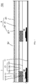
- FIG. 1 is a schematic section of a display assembly
- FIG. 2 is a schematic diagram showing the principle of preventing ambient light reflection by the display assembly in FIG. 1 ;
- FIG. 3 is a schematic diagram showing how light exits from the display assembly in FIG. 1 ;
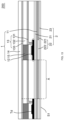
- FIG. 4 is a section of part of a display assembly, in accordance with some embodiments.
- FIG. 5 A is a schematic diagram showing how light exits from the display device in FIG. 4 ;
- FIG. 5 B is a schematic diagram showing how the display assembly in FIG. 4 prevents ambient light from being reflected
- FIG. 6 is a top view of a display panel, in accordance with some embodiments.
- FIG. 7 is a section of part of another display assembly, in accordance with some embodiments.
- FIG. 8 is a schematic section of part of yet another display assembly, in accordance with some embodiments.
- FIG. 9 is a schematic diagram showing steps of manufacturing an optical film group, in accordance with some embodiments.
- FIG. 10 is a schematic diagram showing steps of manufacturing another optical film group, in accordance with some embodiments.
- FIG. 11 is a schematic diagram showing steps of manufacturing yet another optical film group, in accordance with some embodiments.
- FIG. 12 is a section of part of yet another display assembly, in accordance with some embodiments.
- FIG. 13 is a section of part of yet another display assembly, in accordance with some embodiments.
- FIG. 14 is a perspective view of part of a reflective polarizer, in accordance with some embodiments.
- FIG. 15 is a perspective view of part of another reflective polarizer, in accordance with some embodiments.
- first and second are used for descriptive purposes only and are not to be construed as indicating or implying the relative importance or implicitly indicating the number of indicated technical features below. Therefore, a feature defined by the term “first” or “second” may include one or more of the features, either explicitly or implicitly.
- term “plurality” means two or more unless otherwise specified.
- At least one of A, B, and C has a same meaning as “at least one of A, B, or C”, and both include the following combinations of A, B, and C: only A, only B, only C, a combination of A and B, a combination of A and C, a combination of B and C, and a combination of A, B, and C.
- a and/or B includes the following combinations of A and B: only A, only B, and a combination of A and B.
- orientations or positional relationships indicated by terms “center”, “upper”, “lower”, “front”, “rear”, “left”, “right”, “vertical”, “horizontal”, “top”, “bottom”, “inner”, “outer”, etc. are based on orientations or positional relationships shown in the drawings, which merely to facilitate and simplify the description of embodiments of the invention, but not to indicate or imply that the referred devices or elements must have a particular orientation, or must be constructed or operated in a particular orientation. Therefore they should not be construed as limitations to the invention.
- “a plurality of” means two or more unless otherwise specified.
- a display assembly includes a display panel 01 , such as an organic light-emitting diode (OLED) display panel, and a circular polarizer 02 disposed on a display surface of the display panel 01 .
- the circular polarizer 02 is composed of a quarter-wave plate 021 and an absorbing polarizer 023 . If the circular polarizer 02 is not provided, ambient light may enter the display panel 01 from the display surface of the display panel 01 , and then may be reflected by structures such as a metal layer in the display panel 01 . As a result, the reflected ambient light is mixed into light emitted by the display panel 01 , causing the reflected ambient light to interfere with the light emitted by the display panel 01 , which reduces contrast of the display panel 01 .
- OLED organic light-emitting diode
- the ambient light is natural light, and may be resolved into linearly polarized light with two polarization directions perpendicular to each other.
- ambient light 03 is resolved into linearly polarized light with a polarization direction perpendicular to the paper (represented by the dot) and linearly polarized light with a polarization direction parallel to the paper (represented by the line segment with arrows at both ends).
- the linearly polarized light with a polarization direction parallel to a polarization axis of the absorbing polarizer 023 is able to pass through the absorbing polarizer 023
- linearly polarized light with a polarization direction perpendicular to the polarization axis of the absorbing polarizer 023 is not able to pass through the absorbing polarizer 023 and is absorbed by the absorbing polarizer 023 .
- the linearly polarized light with the polarization direction perpendicular to the paper is able to pass through the absorbing polarizer 023 and the linearly polarized light with the polarization direction parallel to the paper is not able to pass through the absorbing polarizer 023 .
- the linearly polarized light with the polarization direction parallel to the polarization axis of the absorbing polarizer 023 is referred to as first linearly polarized light 031 .
- the first linearly polarized light 031 passes through the absorbing polarizer 023 , and then passes through a quarter-wave plate 021 to become circularly polarized light 033 .
- the circularly polarized light 033 is reflected by structures such as a metal layer in the display panel 01 , and then passes through the quarter-wave plate 021 again to become linearly polarized light, which is referred to as second linearly polarized light 032 .
- the quarter-wave plate 021 Due to an effect of the quarter-wave plate 021 , there is a 90° difference between a polarization direction of the second linearly polarized light 032 and the polarization direction of the first linearly polarized light 031 . That is to say, the polarization direction of the second linearly polarized light 032 is perpendicular to the polarization axis of the absorbing polarizer 023 , and the second linearly polarized light 032 is not able to pass through the absorbing polarizer 023 . In this way, the circular polarizer 02 may reduce the ambient light 03 exiting from the display assembly, thereby improving contrast of a display assembly which includes the display panel 01 .
- light 04 emitted by the display panel 01 is also natural light which is still natural light after passing through the quarter-wave plate 021 . That is to say, after passing through the quarter-wave plate 021 , the light 04 can still be resolved into linearly polarized light with two polarization directions perpendicular to each other. For example, as shown in FIG. 3 , the light 04 is resolved into linearly polarized light with a polarization direction perpendicular to the paper (represented by the dot) and linearly polarized light with a polarization direction parallel to the paper (represented by the line segment with arrows at both ends).
- the display assembly 100 includes a display panel 1 and at least one optical film group 2 , and each optical film group 2 is disposed on a display surface S 1 (or a display surface S 2 ) of the display panel 1 .
- the display panel 1 includes a plurality of sub-pixels P.
- the display panel may further include a substrate 11 on which the plurality of sub-pixels P are disposed.
- the display panel 1 is an OLED display panel, and each sub-pixel includes, for example, a light-emitting device 13 and a driver circuit 12 electrically connected to the light-emitting device 13 .
- the display panel 1 is a display panel of another type, for example, a micro light-emitting display (Micro LED) panel, or a liquid crystal display (LCD) panel.
- Micro LED micro light-emitting display
- LCD liquid crystal display
- the optical film group 2 includes a quarter-wave plate 21 , a reflective polarizer 22 and an absorbing polarizer 23 sequentially arranged in a direction away from the display panel 1 .
- the reflective polarizer 22 includes a reflective portion 221 .
- the reflective portion 221 is capable of allowing light with a polarization direction parallel to a polarization axis of the reflective polarizer 22 to pass through and reflecting light with a polarization direction perpendicular to the polarization axis of the reflective polarizer 22 .
- An orthographic projection of an effective light-emitting area A of at least one sub-pixel (for example, an effective light-emitting area of a light-emitting device in a sub-pixel of an OLED display panel) on a plane parallel to the display surface S 1 of the display panel 1 is substantially within an orthographic projection of the reflective portion 221 on the plane.
- the plane overlaps with, for example, the surface of the substrate 11 facing the plurality of sub-pixels P. The following embodiments are described by taking an example in which the plane overlaps with this surface of the substrate 11 .
- the absorbing polarizer 23 is capable of allowing light with a polarization direction parallel to a polarization axis of the absorbing polarizer 23 to pass through and absorbing light with a polarization direction perpendicular to the polarization axis of the absorbing polarizer 23 .
- the polarization axis of the reflective polarizer 22 is parallel to the polarization axis of the absorbing polarizer 23 .
- the display panel 1 being the OLED display panel as an example, and the display panel of another type may refer to the description related to the OLED display panel.
- the light-emitting device 13 includes a first electrode 131 and a second electrode 133 , and a light-emitting functional layer 132 disposed between the first electrode 131 and the second electrode 133 .
- the light-emitting functional layer 132 may be a single-layer structure including an organic emission layer or a multiple-layer structure including an organic emission layer.
- the light-emitting functional layer 132 includes at least one of an electron transporting layer (ETL), an electron injection layer (EIL), a hole transporting layer (HTL) and a hole injection layer (HIL).
- the light-emitting functional layer 132 may be formed by ink-jet printing or evaporation.
- the first electrode 131 of the light-emitting device 13 may be an anode and the second electrode 133 may be a cathode. Or, the first electrode 131 of the light-emitting device 13 may be a cathode and the second electrode 133 may be an anode.
- the effective light-emitting area A of the sub-pixel refers to an area actually used for image display in the sub-pixel during display.
- the whole light-emitting functional layer 132 is used for emitting light, but an orthographic projection of a portion of the light-emitting functional layer 132 on the substrate 11 may overlap with an orthographic projection of the driver circuit 12 (which is non-transparent) on the substrate 11 , which means that light emitted from this portion of the light-emitting functional layer 132 is blocked by the driver circuit 12 and thus is hardly observed. Therefore, although this portion of the light-emitting functional layer 132 emits light, it does not make a contribution to the image display, and this portion is not included in the effective light-emitting area A of the light-emitting device 13 .
- the display surface S 1 of the display panel 1 refers to a surface of the display panel 1 through which a user can watch the image displayed by the display panel 1 .
- the display panel 1 may be a display panel capable of emitting light from one side, for example, a top-emitting display panel (shown in FIG. 7 ) or a bottom-emitting display panel (shown in FIG. 4 ).
- the display panel 1 may also be a double-sided light-emitting display panel (shown in FIG. 8 ), that is, a display panel capable of emitting light from two sides, and both sides of the display panel 1 can display images.
- light 4 emitted from the effective light-emitting area A of the sub-pixel is natural light, and the light 4 is still natural light after passing through the quarter-wave plate 21 , which may be resolved into linearly polarized light with two polarization directions perpendicular to each other.
- the linearly polarized light with the polarization direction parallel to the polarization axis of the reflective polarizer 22 is able to pass through the reflective polarizer 22 .
- the linearly polarized light with the polarization direction perpendicular to the polarization axis of the reflective polarizer 22 is not able to pass through the reflective polarizer 22 , and is reflected by the reflective polarizer 22 .
- the linearly polarized light reflected by the reflective polarizer 22 is called first linearly polarized light 41 .
- the first linearly polarized light 41 passes through the quarter-wave plate 21 and becomes circularly polarized light 43 .
- the circularly polarized light 43 is reflected by the display panel 1 , and becomes second linearly polarized light 42 after passing through the quarter-wave plate 21 .
- the second linearly polarized light 42 is able to pass through the reflective polarizer 22 and the absorbing polarizer 23 whose polarization axis is parallel to the polarization axis of the reflective polarizer 22 , thereby increasing light exiting from the display assembly 100 and improving contrast of the display assembly 100 .
- the reflective polarizer 22 may have various structures.
- the reflective polarizer 22 may include a polarizer (such as an absorbing polarizer) and reflective films attached to two opposite surfaces of the polarizer respectively.
- a polarizer such as an absorbing polarizer
- reflective films attached to two opposite surfaces of the polarizer respectively.
- the reflective polarizer 22 is a wire-gird polarizer.
- the wire-gird polarizer includes a plurality of metal wires 2202 which are arranged at equal intervals. Surfaces of the metal wires 2202 can reflect light, so that the wire-gird polarizer can reflect linearly polarized light which can not pass through the wire-gird polarizer.
- a polarization axis of the wire-gird polarizer is perpendicular to an extension direction of the metal wires 2202 .
- the linearly polarized light with the polarization direction parallel to the extension direction of the metal wires 2202 is able to pass through the wire-gird polarizer.
- the linearly polarized light with the polarization direction perpendicular to the extension direction of the metal wires 2202 is not able to pass through the wire-gird polarizer, and is reflected by the surface of the wire-gird polarizer.
- a width of each metal wire 2202 is in a range from 50 nm to 60 nm, and a fill factor of the wire-gird polarizer is in a range from 0.4 to 0.6.
- a width of each metal wire 2202 may be 50 nm, 52 nm, 55 nm, 58 nm or 60 nm, and the fill factor of the wire-gird polarizer may be 0.4, 0.45, 0.5, 0.55 or 0.6. In this way, the light emitted from the display assembly 100 may be further increased, and the original linearly polarized light with two directions perpendicular to each other may be emitted from the display assembly 100 .
- the fill factor of the wire-gird polarizer equals to an area ratio of the metal wires to the wire-gird polarizer.
- the width of each metal wire 2202 is 50 nm, an interval between two adjacent metal wires 2202 is 50 nm, and the fill factor is approximately 0.5.
- the width of each metal wire 2202 is 50 nm, the interval between two adjacent metal wires 2202 is 75 nm, and the fill factor is approximately 0.4.
- the display panel 1 may have various structures.
- the display panel 1 is the OLED display panel
- the first electrode 131 of the light-emitting device 13 is an anode
- the second electrode 133 of the light-emitting device 13 is a cathode.
- the display panel 1 has an active area AA used for display and a peripheral region S disposed around the active area AA.
- the plurality of sub-pixels P are located in the active area AA.
- the peripheral region S may be used for arranging wires and circuits, for example, a gate driver circuit.
- Each sub-pixel P includes the driver circuit 12 and the light-emitting device 13 .
- the driver circuit 12 may include a plurality of thin film transistors including a driving transistor Td.
- FIG. 4 is a section of part of the display panel 100 taken along a line passing through the driving transistor Td.
- FIG. 4 only shows the driving transistor Td, and does not show other thin film transistors. With regard to the structure of the other thin film transistors, reference may be made to the structure of the driving transistor Td.
- the display panel 1 includes a plurality of metal layers, for example, a source and drain metal layer (including a source and a drain of each thin film transistor) and a gate metal layer (including a gate of each thin film transistor and a gate line electrically connected to the gate).
- a source and drain metal layer including a source and a drain of each thin film transistor
- a gate metal layer including a gate of each thin film transistor and a gate line electrically connected to the gate.
- the driving transistor Td includes a gate, a source and a drain, and the source or the drain is electrically connected to the first electrode 131 of the light-emitting device 13 .
- the display panel 1 may further include a pixel defining layer 15 and an encapsulation layer 14 that is disposed on a side of the second electrode 133 away from the substrate 11 .
- the pixel defining layer 15 includes a plurality of openings, and a light-emitting functional layer 132 of a light-emitting device 13 is disposed in each opening.
- the encapsulation layer 14 may be used to prevent water and oxygen from reaching and entering the light-emitting device 13 .
- the display panel 1 may be a top-emitting display panel, a bottom-emitting display panel or a double-sided light-emitting display panel according to different light-emitting directions. Display panels 1 with different light-emitting directions will be described exemplarily with reference to FIGS. 4 , 7 and 8 .
- the display panel 1 is the bottom-emitting display panel.
- the display panel 1 has a display surface S 1 located on a side of the driver circuits 12 away from the light-emitting devices 13 .
- the first electrode 131 is transparent.
- the first electrode 131 is made of indium tin oxide (ITO), indium zinc oxide (IZO), zinc oxide (ZnO), indium oxide (In 2 O 3 ) or the like.
- the second electrode 133 is opaque.
- the second electrode 133 is made of silver or aluminum.
- the optical film group 2 is disposed on a surface of the substrate 11 facing away from the encapsulation layer 14 .
- the quarter-wave plate 21 is in contact with a surface of the substrate 11 facing away from the plurality of sub-pixels (i.e., a surface of the substrate 11 facing away from each driver circuit 12 and each light-emitting device 13 ).
- the reflective polarizer 22 is in contact with a surface of the quarter-wave plate 21 facing away from the substrate 11
- the absorbing polarizer 23 is in contact with a surface of the reflective polarizer 22 facing away from the quarter-wave plate 21 .
- a transparent optical glue may be used to attach one to another of the above components to implement the contact.
- the reflective polarizer 22 of the display panel 1 further includes a plurality of light-transmissive portions 222 .
- the light-transmissive portions 222 are capable of allowing light with two polarization directions perpendicular to each other to pass through.
- An orthographic projection of non-light-emitting area (such as an area occupied by a driver circuit 12 ) of each sub-pixel on the substrate 11 is substantially within an orthographic projection of a respective one of the plurality of light-transmissive portions 222 on the substrate 11 .
- the plurality of light-transmissive portions 222 include at least one transparent portion and/or at least one opening.
- the plurality of light-transmissive portions 222 include a plurality of transparent portions.
- the plurality of light-transmissive portions 222 include a plurality of openings.
- the plurality of light-transmissive portions 222 include at least one transparent portion and at least one opening.
- the transparent portion serving as the light-transmissive portion 222 is made of a transparent material.
- the opening serving as the light-transmissive portion may be formed by removing a corresponding portion in the reflective polarizer 22 .
- the orthographic projection of the reflective portion 221 on the substrate 11 substantially coincides with orthographic projections of the effective light-emitting areas A of the effective light-emitting areas (such as, the effective light-emitting area of the light-emitting devices 13 ) of the plurality of sub-pixels on the substrate 11 .
- the driver circuit 12 in each sub-pixel is closer to the display surface S 1 relative to the light-emitting device 13 .
- a part of the linearly polarized light of the ambient light passes through the absorbing polarizer 23 , reaches the driver circuit 12 and is reflected by the driver circuit 12 .
- the part which reaches the driver circuit 12 and is reflected by the driver circuit 12 passes through the plurality of light-transmissive portions 222 and reaches the absorbing polarizer 23 , and then is absorbed by the absorbing polarizer 23 .
- this part will not be reflected to the display panel 1 by the reflective portion 221 , which may prevent the driver circuit 12 from reflecting the ambient light, i.e., a reflection of the display panel 1 to the ambient light may be reduced, thereby improving the contrast of the display assembly 100 .
- the reflective portion 221 of the reflective polarizer 22 may increase the light emitted from the display assembly 100 .
- the reflective polarizer 22 may be a wire-gird polarizer.
- the reflective polarizer 22 includes a transparent base 2201 and metal wires 2202 disposed on the transparent base 2201 .
- the quarter-wave plate 21 is disposed on surfaces of the metal wires 2202 facing away from the transparent base 2201
- the absorbing polarizer 23 is disposed on a side of the transparent base 2201 away from the metal wires 2202 .
- the openings which serving as the light-transmissive portions 222 are formed.
- the transparent base 2201 is transparent, by only removing multiple portions of the metal wires 2202 , the transparent portions which serve as the light-transmissive portion 222 are formed.
- the transparent portion corresponds to a portion on which no metal wires of the transparent base 2201 are located.
- a portion on which metal wires 2202 are located of the transparent base 2201 and the metal wires 2202 thereon jointly serve as the reflective portion 221 of the reflective polarizer 22 .
- the display panel 1 is the top-emitting display panel.
- the display panel 1 has a display surface S 2 which is located on a surface of a layer including the driver circuits 12 proximate to the light-emitting devices 13 .
- the first electrode 131 is opaque.
- the first electrode 131 may be a multiple-layer structure composed of at least one ITO (Indium Tin Oxides) layer and at least one silver (Ag) layer.
- the first electrode 131 is a three-layer structure composed of an ITO layer, an Ag layer and an ITO layer that are stacked.
- the second electrode 133 is transparent or translucent, for example, the second electrode 133 is composed of a silver layer that is thin enough to be transparent or translucent.
- the at least one optical film group 2 includes one optical film group 2 , which is disposed on a side of the encapsulation layer 14 away from the substrate 11 .
- the quarter-wave plate 21 is disposed on a side of the plurality of sub-pixels away from the substrate 11 .
- the quarter-wave plate 21 may be in contact with a surface of the encapsulation layer 14 facing away from the substrate 11
- the reflective polarizer 22 is in contact with a surface of the quarter-wave plate 21 facing away from the plurality of sub-pixels
- the absorbing polarizer 23 is in contact with a surface of the reflective polarizer 22 facing away from the quarter-wave plate 21 .
- orthographic projections of non-light-emitting areas are within the orthographic projection of the reflective portion 221 of the reflective polarizer 22 on the substrate 11 .
- the reflective portion 221 covers the entire active area AA of the display panel 1 .
- the reflective portion 221 may have a structure of a complete plate.
- the light-emitting device 13 in each sub-pixel is closer to the display surface S 2 relative to the driver circuit 12 .
- the linearly polarized light of the ambient light passing through the absorbing polarizer 23 first reaches the light-emitting device 13 . Since the first electrode 131 of the light-emitting device 13 is opaque, the linearly polarized light from the ambient light and passing through the absorbing polarizer 23 will not reach the driver circuit 12 , that is to say, a problem that the driver circuit 12 reflects the ambient light hardly occurs in each sub-pixel.
- the reflective portion 221 of the reflective polarizer 22 may cover the entire active area AA, and the light emitted from the display assembly 100 may be increased while the contrast of the display assembly 100 may be ensured.
- the reflective polarizer 22 may be a wire-gird polarizer (shown as FIG. 14 ) which includes a transparent base 2201 and metal wires 2202 disposed on the transparent base 2201 .
- the quarter-wave plate 21 may be disposed on surfaces of the metal wires 2202 facing away from the transparent base 2201
- the absorbing polarizer 23 may be disposed on a surface of the transparent base 2201 facing away from the metal wires 2202 .
- the display panel 1 is the double-sided light-emitting display panel, and the display panel 1 has two display surfaces, i.e., a display surface S 1 and a display surface S 2 .
- the display surface S 1 is located on a side of the driver circuits 12 away from the light-emitting devices 13 and the display surface S 2 is located on a side of the driver circuits 12 proximate to the light-emitting devices 13 .
- the first electrode 131 and the second electrode 133 are both transparent.
- the first electrode 131 is made of indium tin oxide (ITO), indium zinc oxide (IZO), zinc oxide (ZnO), indium oxide (In 2 O 3 ) or the like.
- the second electrode 133 is composed of a silver layer that is thin enough to be transparent or translucent.
- the at least one optical film group 2 includes a first optical film group 2 A and a second optical film group 2 B.
- the first optical film group 2 A is disposed on a side of the substrate 11 away from the plurality of sub-pixels, that is, the display surface S 1 of the display panel 1 .
- the second optical film group 2 B is disposed on a side of the plurality of sub-pixels away from the substrate 11 , that is, the display surface S 2 of the display panel 1 .
- the quarter-wave plate 21 A is in contact with a surface of the substrate 11 facing away from the plurality of sub-pixels
- the reflective polarizer 22 A is in contact with a surface of the quarter-wave plate 21 A facing away from the substrate 11
- the absorbing polarizer 23 A is in contact with a surface of the reflective polarizer 22 A facing away from the quarter-wave plate 21 A.
- the quarter-wave plate 21 B is in contact with a surface of the plurality of sub-pixels facing away from the substrate 11
- the reflective polarizer 22 B is in contact with a surface of the quarter-wave plate 21 B facing away from the plurality of sub-pixels
- the absorbing polarizer 23 B is in contact with a surface of the reflective polarizer 22 B facing away from the quarter-wave plate 21 B.
- the reflective polarizer 22 A in the first optical film group 2 A includes a plurality of light-transmissive portions 222 A.
- An orthographic projection of a non-light-emitting area (such as the area occupied by the driver circuit 12 ) of each sub-pixel on the substrate 11 is within an orthographic projection of a respective one of the plurality of light-transmissive portion 222 A on the substrate 11 .
- Orthographic projections of non-light-emitting areas of the plurality of sub-pixels on the substrate 11 are within an orthographic projection of the reflective portion 221 A of the reflective polarizer 22 B in the second optical film group 2 B on the substrate 11 .
- the reflective polarizers may be wire-gird polarizers.
- the reflective polarizer 22 A in the first optical film group 2 A includes a first transparent base and first metal wires disposed on the first transparent base
- the reflective polarizer 22 B in the second optical film group 2 B includes a second transparent base and second metal wires disposed on the second transparent base.
- the quarter-wave plate 21 A is disposed on surfaces of the first metal wires facing away from the first transparent base, and the absorbing polarizer 22 A is disposed on a surface of the first transparent base facing away from the first metal wires.
- the quarter-wave plate 21 B is disposed on surfaces of the second metal wires facing away from the second transparent base, and the absorbing polarizer 22 B is disposed on a surface of the second transparent base facing away from the second metal wires.
- the optical film group 2 is disposed on a side of the substrate 11 away from the encapsulation layer 14 , and a transparent adhesive may be provided onto a surface of the quarter-wave plate 21 facing away from the reflective polarizer 22 to adhere the optical film group 2 to the substrate 11 during the process of manufacturing the display assembly 100 .
- the display assembly may be the display assembly 200 shown in FIGS. 12 and 13 .
- the display assembly 200 includes a substrate 11 , a plurality of sub-pixels disposed on the substrate 11 , a quarter-wave plate 21 , a reflective polarizer 22 and an absorbing polarizer 23 .
- Each sub-pixel includes a light-emitting device 13 and a driver circuit 12 electrically connected to the light-emitting device 13 .
- the quarter-wave plate 21 is disposed between the substrate 11 and the plurality of sub-pixels.
- the absorbing polarizer 23 is disposed on a surface of the substrate 11 facing away from the quarter-wave plate 21 .
- the reflective polarizer 22 is disposed between the quarter-wave plate 21 and the absorbing polarizer 23 .
- the structure of the display panel 1 in the display assembly 200 may be referred to the description of the display panel 1 in the display assembly 100 .
- components such as the substrate 11 , the quarter-wave plate 21 , the reflective polarizer 22 , the absorbing polarizer 23 in the display assembly 200 , reference may be made to the above description of the components in the display assembly 100 . Details will not be repeated here again.
- the optical film group 2 including the quarter-wave plate 21 , the reflective polarizer 22 and the absorbing polarizer 23 is integrated with the display panel 1 , and the light emitted from the display assembly 200 and the contrast of the display assembly 200 may also be increased.
- a display surface S 1 of the display panel 1 in FIG. 12 is located on a side of each driver circuit 12 away from a corresponding light-emitting device 13 , that is, the display panel 1 in FIG. 12 is a bottom-emitting display panel.
- the display panel 1 may be a top-emitting display panel or a double-sided light-emitting display panel.
- the quarter-wave plate 21 , the reflective polarizer 22 and the absorbing polarizer 23 need to be disposed on the display surface of the display panel 1 , and reference may be made to arrangements of the quarter-wave plate 21 , the reflective polarizer 22 , and the absorbing polarizer 23 in the above display panel 100 , and details will not be repeated here again.
- the reflective polarizer 22 is disposed between the quarter-wave plate 21 and the substrate 11 .
- the reflective polarizer 22 is in contact with a surface of the substrate 11 proximate to the light-emitting device 13
- the quarter-wave plate 21 is in contact with a surface of the reflective polarizer 22 away from the substrate 11
- the absorbing polarizer 23 is in contact with a surface of the substrate 11 away from the light-emitting device 13 .
- the substrate 11 may serve as a base for the quarter-wave plate 21 , the reflective polarizer 22 and the absorbing polarizer 23 .
- the reflective polarizer 22 is a wire-gird polarizer
- metal wires may be formed on the substrate 11 , so that a thickness of the display assembly 200 may be reduced.
- the wire-gird polarizer does not require an additional transparent base, light transmittance of the display assembly 200 may be improved.
- the reflective polarizer 22 is disposed between the substrate 11 and the absorbing polarizer 23 .
- the quarter-wave plate 21 is in contact with the surface of the substrate 11 proximate to the light-emitting device 13
- the reflective polarizer 22 is in contact with the surface of the substrate 11 away from the light-emitting device 13
- the absorbing polarizer 23 is in contact with the surface of the reflective polarizer 22 away from the substrate 11 .
- the substrate 11 may serve as a base for the quarter-wave plate 21 , the reflective polarizer 22 and the absorbing polarizer 23 .
- the thickness of the display assembly 200 may also be reduced, and the light transmittance of the display assembly 200 may be improved.
- an analysis process of converting a polarization state of light, emitted by the light-emitting device 13 , by the quarter-wave plate 21 , the reflective polarizer 22 and the absorbing polarizer 23 in the display assembly 200 , to realize a light emission is similar to that of the optical film group 2 in the display assembly 100 , and details will not be repeated here again.
- the wire-gird polarizer includes a plurality of metal wires 2202 which are arranged at equal intervals.
- a width range of each metal wire 2202 is from 50 nm to 60 nm, and a fill factor of the wire-gird polarizer is in a range from 0.4 to 0.6.
- the width of each metal wire 2202 may be 50 nm, 52 nm, 55 nm, 58 nm or 60 nm, and the fill factor of the wire-gird polarizer may be 0.4, 0.45, 0.5, 0.55 or 0.6.
- the light output of the display assembly 200 may be further improved, and linearly polarized light with two directions perpendicular to each other may be emitted by the display assembly 200 .
- the fill factor of the wire-gird polarizer equals to an area ratio of the metal wires 2202 to the wire-gird polarizer.
- the metal wires 2202 are formed on a surface of the transparent base 2201 .
- the quarter-wave plate 21 is attached to surfaces of the metal wires 2202 facing away from the transparent base 2201 .
- the absorbing polarizer 23 is attached to a surface of the transparent base 2201 facing away from the metal wires 2202 .
- the metal wires 2202 are first formed on a surface of the transparent base 2201 . Then, the absorbing polarizer 23 is attached to another surface of the transparent base 2201 facing away from the metal wires 2202 . Finally, the quarter-wave plate 21 is attached to a surface of the metal wires 2202 facing away from the transparent base 2201 .
- the quarter-wave plate 21 is attached to the display panel 1 (for example, attached to the substrate 11 ).
- the metal wires 2202 is formed on a surface of the transparent base 2201 , and the absorbing polarizer 23 is attached to another surface of the transparent base 2201 facing away from the metal wires 2202 .
- surfaces of the metal wires 2202 facing away from the transparent base 2201 and a surface of the quarter-wave plate 21 facing away from the display panel 1 are attached.
- Some embodiments of the present disclosure provide a display device including the display assembly 100 or 200 described above and a driving assembly.
- the driving assembly is configured to provide display data and control signals to the display assembly 100 .
- the driving assembly may include at least one of a power circuit (Power IC), a timing control circuit (TCON IC), a gray scale circuit, a source driver IC or a gate driver IC.
- the display device has the same beneficial effects as the display assembly 100 , and details will not be repeated here again.
- the display device provided by some embodiments of the present disclosure may be any product or component having a display function, such as a mobile phone, a tablet computer, a television, a display, a notebook computer, a digital camera, a navigator and the like.
- some embodiments of the present disclosure provide an optical film group, which may be the optical film group 2 , 2 A, or 2 B in the display assembly 100 described above.
- the optical film group has the same beneficial effects as the display assembly 100 , and details will not be repeated here again.
Landscapes
- Physics & Mathematics (AREA)
- Optics & Photonics (AREA)
- General Physics & Mathematics (AREA)
- Nonlinear Science (AREA)
- Mathematical Physics (AREA)
- Chemical & Material Sciences (AREA)
- Crystallography & Structural Chemistry (AREA)
- Engineering & Computer Science (AREA)
- Manufacturing & Machinery (AREA)
- Electroluminescent Light Sources (AREA)
Abstract
Description
Claims (20)
Applications Claiming Priority (2)
| Application Number | Priority Date | Filing Date | Title |
|---|---|---|---|
| CN201910702425.X | 2019-07-31 | ||
| CN201910702425.XA CN110426859B (en) | 2019-07-31 | 2019-07-31 | Optical film, display assembly and display device |
Publications (2)
| Publication Number | Publication Date |
|---|---|
| US20210036264A1 US20210036264A1 (en) | 2021-02-04 |
| US11575111B2 true US11575111B2 (en) | 2023-02-07 |
Family
ID=68413357
Family Applications (1)
| Application Number | Title | Priority Date | Filing Date |
|---|---|---|---|
| US16/887,438 Active 2041-07-07 US11575111B2 (en) | 2019-07-31 | 2020-05-29 | Optical film group, display assembly and display device |
Country Status (2)
| Country | Link |
|---|---|
| US (1) | US11575111B2 (en) |
| CN (1) | CN110426859B (en) |
Families Citing this family (13)
| Publication number | Priority date | Publication date | Assignee | Title |
|---|---|---|---|---|
| CN114188368A (en) * | 2020-09-14 | 2022-03-15 | 华为技术有限公司 | OLED display module and display device |
| WO2022104538A1 (en) * | 2020-11-17 | 2022-05-27 | 京东方科技集团股份有限公司 | Optical film and manufacturing method therefor, and reflective liquid crystal display panel and display device |
| CN115376421A (en) * | 2021-05-19 | 2022-11-22 | 上海和辉光电股份有限公司 | Display panel, manufacturing method thereof, and display device |
| CN114459598B (en) * | 2021-05-20 | 2024-05-14 | 义明科技股份有限公司 | Light sensing integrated circuit and electronic device using same |
| CN113448101A (en) * | 2021-06-28 | 2021-09-28 | 歌尔股份有限公司 | Optical module and head-mounted display device |
| WO2023028787A1 (en) * | 2021-08-30 | 2023-03-09 | 京东方科技集团股份有限公司 | Display substrate and display device |
| WO2023028828A1 (en) * | 2021-08-31 | 2023-03-09 | 华为技术有限公司 | Optical stack structure, display module, terminal, and relevant manufacturing method |
| US12566330B2 (en) | 2021-10-22 | 2026-03-03 | Samsung Display Co., Ltd. | Head mount display device |
| WO2023127908A1 (en) * | 2021-12-27 | 2023-07-06 | 富士フイルム株式会社 | Virtual reality display device |
| CN116047779B (en) * | 2022-05-18 | 2023-11-07 | 荣耀终端有限公司 | Optical module, display screen and electronic equipment |
| CN117908268A (en) * | 2022-10-10 | 2024-04-19 | 群创光电股份有限公司 | Electronic Devices |
| CN115840305B (en) * | 2022-11-10 | 2025-08-22 | 昆山国显光电有限公司 | Display panel and display device |
| KR20240168509A (en) | 2023-05-22 | 2024-12-02 | 삼성디스플레이 주식회사 | Head mount display devoce |
Citations (11)
| Publication number | Priority date | Publication date | Assignee | Title |
|---|---|---|---|---|
| US20070069635A1 (en) * | 2005-09-27 | 2007-03-29 | Eastman Kodak Company | OLED device having improved contrast |
| US20080237611A1 (en) * | 2007-03-29 | 2008-10-02 | Cok Ronald S | Electroluminescent device having improved contrast |
| US20080252799A1 (en) * | 2007-04-10 | 2008-10-16 | Samsung Electronics Co., Ltd. | Wire grid polarizer having dual layer structure and method of fabricating the same |
| US20100177113A1 (en) * | 2007-06-01 | 2010-07-15 | Gregory Gay | Optical system and display |
| CN101783360A (en) | 2009-01-21 | 2010-07-21 | 三星移动显示器株式会社 | Organic light emitting diode display and optical component |
| US20100320494A1 (en) | 2008-05-22 | 2010-12-23 | Kim Sin-Young | Luminance-enhancing polarising plate for an organic light-emitting element |
| WO2014085199A1 (en) | 2012-11-30 | 2014-06-05 | 3M Innovative Properties Company | Emissive display with reflective polarizer |
| CN105264684A (en) | 2013-06-06 | 2016-01-20 | 3M创新有限公司 | Antireflective OLED construction |
| CN105467499A (en) | 2016-01-15 | 2016-04-06 | 京东方科技集团股份有限公司 | Metal wire grating polaroid and manufacturing method thereof, display panel and display device |
| US20180358583A1 (en) * | 2016-08-05 | 2018-12-13 | Boe Technology Group Co., Ltd. | Double-Sided Electroluminescent Display Panel and Display Device |
| CN109256488A (en) | 2018-09-12 | 2019-01-22 | 京东方科技集团股份有限公司 | A kind of OLED display panel and preparation method thereof and display device |
Family Cites Families (2)
| Publication number | Priority date | Publication date | Assignee | Title |
|---|---|---|---|---|
| CN108983483B (en) * | 2018-07-27 | 2021-04-13 | 京东方科技集团股份有限公司 | Display device |
| CN108962959B (en) * | 2018-07-27 | 2021-03-02 | 京东方科技集团股份有限公司 | An organic light-emitting display panel and display device |
-
2019
- 2019-07-31 CN CN201910702425.XA patent/CN110426859B/en active Active
-
2020
- 2020-05-29 US US16/887,438 patent/US11575111B2/en active Active
Patent Citations (15)
| Publication number | Priority date | Publication date | Assignee | Title |
|---|---|---|---|---|
| US20070069635A1 (en) * | 2005-09-27 | 2007-03-29 | Eastman Kodak Company | OLED device having improved contrast |
| US20080237611A1 (en) * | 2007-03-29 | 2008-10-02 | Cok Ronald S | Electroluminescent device having improved contrast |
| US20080252799A1 (en) * | 2007-04-10 | 2008-10-16 | Samsung Electronics Co., Ltd. | Wire grid polarizer having dual layer structure and method of fabricating the same |
| US20100177113A1 (en) * | 2007-06-01 | 2010-07-15 | Gregory Gay | Optical system and display |
| US20100320494A1 (en) | 2008-05-22 | 2010-12-23 | Kim Sin-Young | Luminance-enhancing polarising plate for an organic light-emitting element |
| CN101946195A (en) | 2008-05-22 | 2011-01-12 | Lg化学株式会社 | Luminance-enhancing polarising plate for an organic light-emitting element |
| US20100182552A1 (en) | 2009-01-21 | 2010-07-22 | Soon-Ryong Park | Organic light emitting diode display |
| CN101783360A (en) | 2009-01-21 | 2010-07-21 | 三星移动显示器株式会社 | Organic light emitting diode display and optical component |
| WO2014085199A1 (en) | 2012-11-30 | 2014-06-05 | 3M Innovative Properties Company | Emissive display with reflective polarizer |
| CN105264684A (en) | 2013-06-06 | 2016-01-20 | 3M创新有限公司 | Antireflective OLED construction |
| US20160118448A1 (en) | 2013-06-06 | 2016-04-28 | 3M Innovative Properties Company | Antireflective oled construction |
| CN105467499A (en) | 2016-01-15 | 2016-04-06 | 京东方科技集团股份有限公司 | Metal wire grating polaroid and manufacturing method thereof, display panel and display device |
| US20170205550A1 (en) | 2016-01-15 | 2017-07-20 | Boe Technology Group Co., Ltd. | Metal wire grid polarization plate and manufacturing method thereof, display panel and display device |
| US20180358583A1 (en) * | 2016-08-05 | 2018-12-13 | Boe Technology Group Co., Ltd. | Double-Sided Electroluminescent Display Panel and Display Device |
| CN109256488A (en) | 2018-09-12 | 2019-01-22 | 京东方科技集团股份有限公司 | A kind of OLED display panel and preparation method thereof and display device |
Non-Patent Citations (1)
| Title |
|---|
| Notification of the First Office Action issued in Chinese Patent Application No. 201910702425.X, dated Jan. 19, 2021; with English translation. |
Also Published As
| Publication number | Publication date |
|---|---|
| CN110426859A (en) | 2019-11-08 |
| CN110426859B (en) | 2022-09-09 |
| US20210036264A1 (en) | 2021-02-04 |
Similar Documents
| Publication | Publication Date | Title |
|---|---|---|
| US11575111B2 (en) | Optical film group, display assembly and display device | |
| US11522160B2 (en) | Optical layer having refractive layer covering organic layer and display device including the same | |
| CN111668262B (en) | Display panel | |
| KR102668184B1 (en) | Display device | |
| CN211743193U (en) | Array substrate and display device | |
| US11004914B2 (en) | Display apparatus | |
| WO2020199083A1 (en) | Display substrate and manufacturing method therefor, and display device | |
| CN111584545B (en) | Display device | |
| CN114447034A (en) | Display device | |
| CN113555517A (en) | Display substrate and display device | |
| US9899455B2 (en) | Organic light emitting diode display | |
| CN107507853A (en) | An organic light emitting display panel, its manufacturing method and display device | |
| KR20250005513A (en) | Display panels and display devices | |
| CN113363293A (en) | Display device and electronic apparatus | |
| CN115172626A (en) | Display panel and display device | |
| CN113851507A (en) | transparent display device | |
| US10665794B2 (en) | Flexible display panel and flexible display device | |
| US20230031015A1 (en) | Display apparatus | |
| WO2023245447A1 (en) | Display panel and display device | |
| CN114203777A (en) | Display panel and display device | |
| US20230085460A1 (en) | Display device | |
| US12356830B2 (en) | Display device | |
| CN218570777U (en) | Display panel and display device | |
| CN113130564B (en) | Display device | |
| KR20240141354A (en) | Display device |
Legal Events
| Date | Code | Title | Description |
|---|---|---|---|
| AS | Assignment |
Owner name: BEIJING BOE DISPLAY TECHNOLOGY CO., LTD., CHINA Free format text: ASSIGNMENT OF ASSIGNORS INTEREST;ASSIGNORS:HU, WEIPIN;YANG, HONG;WANG, CHUN;AND OTHERS;REEL/FRAME:052788/0770 Effective date: 20200210 Owner name: BOE TECHNOLOGY GROUP CO., LTD., CHINA Free format text: ASSIGNMENT OF ASSIGNORS INTEREST;ASSIGNORS:HU, WEIPIN;YANG, HONG;WANG, CHUN;AND OTHERS;REEL/FRAME:052788/0770 Effective date: 20200210 |
|
| FEPP | Fee payment procedure |
Free format text: ENTITY STATUS SET TO UNDISCOUNTED (ORIGINAL EVENT CODE: BIG.); ENTITY STATUS OF PATENT OWNER: LARGE ENTITY |
|
| STPP | Information on status: patent application and granting procedure in general |
Free format text: APPLICATION DISPATCHED FROM PREEXAM, NOT YET DOCKETED |
|
| STPP | Information on status: patent application and granting procedure in general |
Free format text: DOCKETED NEW CASE - READY FOR EXAMINATION |
|
| STPP | Information on status: patent application and granting procedure in general |
Free format text: NON FINAL ACTION MAILED |
|
| STPP | Information on status: patent application and granting procedure in general |
Free format text: NOTICE OF ALLOWANCE MAILED -- APPLICATION RECEIVED IN OFFICE OF PUBLICATIONS |
|
| STCF | Information on status: patent grant |
Free format text: PATENTED CASE |