US11532594B2 - Integrated fan-out package and the methods of manufacturing - Google Patents
Integrated fan-out package and the methods of manufacturing Download PDFInfo
- Publication number
- US11532594B2 US11532594B2 US16/418,298 US201916418298A US11532594B2 US 11532594 B2 US11532594 B2 US 11532594B2 US 201916418298 A US201916418298 A US 201916418298A US 11532594 B2 US11532594 B2 US 11532594B2
- Authority
- US
- United States
- Prior art keywords
- device die
- die
- package
- encapsulant
- dies
- Prior art date
- Legal status (The legal status is an assumption and is not a legal conclusion. Google has not performed a legal analysis and makes no representation as to the accuracy of the status listed.)
- Active, expires
Links
Images


Classifications
-
- H—ELECTRICITY
- H01—ELECTRIC ELEMENTS
- H01L—SEMICONDUCTOR DEVICES NOT COVERED BY CLASS H10
- H01L25/00—Assemblies consisting of a plurality of individual semiconductor or other solid state devices ; Multistep manufacturing processes thereof
- H01L25/03—Assemblies consisting of a plurality of individual semiconductor or other solid state devices ; Multistep manufacturing processes thereof all the devices being of a type provided for in the same subgroup of groups H01L27/00 - H01L33/00, or in a single subclass of H10K, H10N, e.g. assemblies of rectifier diodes
- H01L25/04—Assemblies consisting of a plurality of individual semiconductor or other solid state devices ; Multistep manufacturing processes thereof all the devices being of a type provided for in the same subgroup of groups H01L27/00 - H01L33/00, or in a single subclass of H10K, H10N, e.g. assemblies of rectifier diodes the devices not having separate containers
- H01L25/065—Assemblies consisting of a plurality of individual semiconductor or other solid state devices ; Multistep manufacturing processes thereof all the devices being of a type provided for in the same subgroup of groups H01L27/00 - H01L33/00, or in a single subclass of H10K, H10N, e.g. assemblies of rectifier diodes the devices not having separate containers the devices being of a type provided for in group H01L27/00
- H01L25/0652—Assemblies consisting of a plurality of individual semiconductor or other solid state devices ; Multistep manufacturing processes thereof all the devices being of a type provided for in the same subgroup of groups H01L27/00 - H01L33/00, or in a single subclass of H10K, H10N, e.g. assemblies of rectifier diodes the devices not having separate containers the devices being of a type provided for in group H01L27/00 the devices being arranged next and on each other, i.e. mixed assemblies
-
- H—ELECTRICITY
- H01—ELECTRIC ELEMENTS
- H01L—SEMICONDUCTOR DEVICES NOT COVERED BY CLASS H10
- H01L21/00—Processes or apparatus adapted for the manufacture or treatment of semiconductor or solid state devices or of parts thereof
- H01L21/02—Manufacture or treatment of semiconductor devices or of parts thereof
- H01L21/04—Manufacture or treatment of semiconductor devices or of parts thereof the devices having at least one potential-jump barrier or surface barrier, e.g. PN junction, depletion layer or carrier concentration layer
- H01L21/18—Manufacture or treatment of semiconductor devices or of parts thereof the devices having at least one potential-jump barrier or surface barrier, e.g. PN junction, depletion layer or carrier concentration layer the devices having semiconductor bodies comprising elements of Group IV of the Periodic System or AIIIBV compounds with or without impurities, e.g. doping materials
- H01L21/30—Treatment of semiconductor bodies using processes or apparatus not provided for in groups H01L21/20 - H01L21/26
- H01L21/31—Treatment of semiconductor bodies using processes or apparatus not provided for in groups H01L21/20 - H01L21/26 to form insulating layers thereon, e.g. for masking or by using photolithographic techniques; After treatment of these layers; Selection of materials for these layers
- H01L21/3105—After-treatment
- H01L21/31051—Planarisation of the insulating layers
- H01L21/31053—Planarisation of the insulating layers involving a dielectric removal step
-
- H—ELECTRICITY
- H01—ELECTRIC ELEMENTS
- H01L—SEMICONDUCTOR DEVICES NOT COVERED BY CLASS H10
- H01L21/00—Processes or apparatus adapted for the manufacture or treatment of semiconductor or solid state devices or of parts thereof
- H01L21/02—Manufacture or treatment of semiconductor devices or of parts thereof
- H01L21/04—Manufacture or treatment of semiconductor devices or of parts thereof the devices having at least one potential-jump barrier or surface barrier, e.g. PN junction, depletion layer or carrier concentration layer
- H01L21/50—Assembly of semiconductor devices using processes or apparatus not provided for in a single one of the subgroups H01L21/06 - H01L21/326, e.g. sealing of a cap to a base of a container
- H01L21/56—Encapsulations, e.g. encapsulation layers, coatings
-
- H—ELECTRICITY
- H01—ELECTRIC ELEMENTS
- H01L—SEMICONDUCTOR DEVICES NOT COVERED BY CLASS H10
- H01L21/00—Processes or apparatus adapted for the manufacture or treatment of semiconductor or solid state devices or of parts thereof
- H01L21/70—Manufacture or treatment of devices consisting of a plurality of solid state components formed in or on a common substrate or of parts thereof; Manufacture of integrated circuit devices or of parts thereof
- H01L21/71—Manufacture of specific parts of devices defined in group H01L21/70
- H01L21/768—Applying interconnections to be used for carrying current between separate components within a device comprising conductors and dielectrics
- H01L21/76838—Applying interconnections to be used for carrying current between separate components within a device comprising conductors and dielectrics characterised by the formation and the after-treatment of the conductors
- H01L21/76885—By forming conductive members before deposition of protective insulating material, e.g. pillars, studs
-
- H—ELECTRICITY
- H01—ELECTRIC ELEMENTS
- H01L—SEMICONDUCTOR DEVICES NOT COVERED BY CLASS H10
- H01L23/00—Details of semiconductor or other solid state devices
- H01L23/28—Encapsulations, e.g. encapsulating layers, coatings, e.g. for protection
- H01L23/31—Encapsulations, e.g. encapsulating layers, coatings, e.g. for protection characterised by the arrangement or shape
- H01L23/3107—Encapsulations, e.g. encapsulating layers, coatings, e.g. for protection characterised by the arrangement or shape the device being completely enclosed
-
- H—ELECTRICITY
- H01—ELECTRIC ELEMENTS
- H01L—SEMICONDUCTOR DEVICES NOT COVERED BY CLASS H10
- H01L23/00—Details of semiconductor or other solid state devices
- H01L23/34—Arrangements for cooling, heating, ventilating or temperature compensation ; Temperature sensing arrangements
- H01L23/36—Selection of materials, or shaping, to facilitate cooling or heating, e.g. heatsinks
- H01L23/367—Cooling facilitated by shape of device
- H01L23/3675—Cooling facilitated by shape of device characterised by the shape of the housing
-
- H—ELECTRICITY
- H01—ELECTRIC ELEMENTS
- H01L—SEMICONDUCTOR DEVICES NOT COVERED BY CLASS H10
- H01L23/00—Details of semiconductor or other solid state devices
- H01L23/48—Arrangements for conducting electric current to or from the solid state body in operation, e.g. leads, terminal arrangements ; Selection of materials therefor
- H01L23/481—Internal lead connections, e.g. via connections, feedthrough structures
-
- H—ELECTRICITY
- H01—ELECTRIC ELEMENTS
- H01L—SEMICONDUCTOR DEVICES NOT COVERED BY CLASS H10
- H01L23/00—Details of semiconductor or other solid state devices
- H01L23/52—Arrangements for conducting electric current within the device in operation from one component to another, i.e. interconnections, e.g. wires, lead frames
- H01L23/522—Arrangements for conducting electric current within the device in operation from one component to another, i.e. interconnections, e.g. wires, lead frames including external interconnections consisting of a multilayer structure of conductive and insulating layers inseparably formed on the semiconductor body
- H01L23/528—Geometry or layout of the interconnection structure
-
- H—ELECTRICITY
- H01—ELECTRIC ELEMENTS
- H01L—SEMICONDUCTOR DEVICES NOT COVERED BY CLASS H10
- H01L23/00—Details of semiconductor or other solid state devices
- H01L23/52—Arrangements for conducting electric current within the device in operation from one component to another, i.e. interconnections, e.g. wires, lead frames
- H01L23/538—Arrangements for conducting electric current within the device in operation from one component to another, i.e. interconnections, e.g. wires, lead frames the interconnection structure between a plurality of semiconductor chips being formed on, or in, insulating substrates
- H01L23/5389—Arrangements for conducting electric current within the device in operation from one component to another, i.e. interconnections, e.g. wires, lead frames the interconnection structure between a plurality of semiconductor chips being formed on, or in, insulating substrates the chips being integrally enclosed by the interconnect and support structures
-
- H—ELECTRICITY
- H01—ELECTRIC ELEMENTS
- H01L—SEMICONDUCTOR DEVICES NOT COVERED BY CLASS H10
- H01L24/00—Arrangements for connecting or disconnecting semiconductor or solid-state bodies; Methods or apparatus related thereto
- H01L24/01—Means for bonding being attached to, or being formed on, the surface to be connected, e.g. chip-to-package, die-attach, "first-level" interconnects; Manufacturing methods related thereto
- H01L24/02—Bonding areas ; Manufacturing methods related thereto
- H01L24/04—Structure, shape, material or disposition of the bonding areas prior to the connecting process
- H01L24/05—Structure, shape, material or disposition of the bonding areas prior to the connecting process of an individual bonding area
-
- H—ELECTRICITY
- H01—ELECTRIC ELEMENTS
- H01L—SEMICONDUCTOR DEVICES NOT COVERED BY CLASS H10
- H01L24/00—Arrangements for connecting or disconnecting semiconductor or solid-state bodies; Methods or apparatus related thereto
- H01L24/01—Means for bonding being attached to, or being formed on, the surface to be connected, e.g. chip-to-package, die-attach, "first-level" interconnects; Manufacturing methods related thereto
- H01L24/18—High density interconnect [HDI] connectors; Manufacturing methods related thereto
- H01L24/19—Manufacturing methods of high density interconnect preforms
-
- H—ELECTRICITY
- H01—ELECTRIC ELEMENTS
- H01L—SEMICONDUCTOR DEVICES NOT COVERED BY CLASS H10
- H01L24/00—Arrangements for connecting or disconnecting semiconductor or solid-state bodies; Methods or apparatus related thereto
- H01L24/01—Means for bonding being attached to, or being formed on, the surface to be connected, e.g. chip-to-package, die-attach, "first-level" interconnects; Manufacturing methods related thereto
- H01L24/18—High density interconnect [HDI] connectors; Manufacturing methods related thereto
- H01L24/20—Structure, shape, material or disposition of high density interconnect preforms
-
- H—ELECTRICITY
- H01—ELECTRIC ELEMENTS
- H01L—SEMICONDUCTOR DEVICES NOT COVERED BY CLASS H10
- H01L24/00—Arrangements for connecting or disconnecting semiconductor or solid-state bodies; Methods or apparatus related thereto
- H01L24/73—Means for bonding being of different types provided for in two or more of groups H01L24/10, H01L24/18, H01L24/26, H01L24/34, H01L24/42, H01L24/50, H01L24/63, H01L24/71
-
- H—ELECTRICITY
- H01—ELECTRIC ELEMENTS
- H01L—SEMICONDUCTOR DEVICES NOT COVERED BY CLASS H10
- H01L24/00—Arrangements for connecting or disconnecting semiconductor or solid-state bodies; Methods or apparatus related thereto
- H01L24/91—Methods for connecting semiconductor or solid state bodies including different methods provided for in two or more of groups H01L24/80 - H01L24/90
- H01L24/92—Specific sequence of method steps
-
- H—ELECTRICITY
- H01—ELECTRIC ELEMENTS
- H01L—SEMICONDUCTOR DEVICES NOT COVERED BY CLASS H10
- H01L25/00—Assemblies consisting of a plurality of individual semiconductor or other solid state devices ; Multistep manufacturing processes thereof
- H01L25/03—Assemblies consisting of a plurality of individual semiconductor or other solid state devices ; Multistep manufacturing processes thereof all the devices being of a type provided for in the same subgroup of groups H01L27/00 - H01L33/00, or in a single subclass of H10K, H10N, e.g. assemblies of rectifier diodes
- H01L25/04—Assemblies consisting of a plurality of individual semiconductor or other solid state devices ; Multistep manufacturing processes thereof all the devices being of a type provided for in the same subgroup of groups H01L27/00 - H01L33/00, or in a single subclass of H10K, H10N, e.g. assemblies of rectifier diodes the devices not having separate containers
- H01L25/065—Assemblies consisting of a plurality of individual semiconductor or other solid state devices ; Multistep manufacturing processes thereof all the devices being of a type provided for in the same subgroup of groups H01L27/00 - H01L33/00, or in a single subclass of H10K, H10N, e.g. assemblies of rectifier diodes the devices not having separate containers the devices being of a type provided for in group H01L27/00
- H01L25/0657—Stacked arrangements of devices
-
- H—ELECTRICITY
- H01—ELECTRIC ELEMENTS
- H01L—SEMICONDUCTOR DEVICES NOT COVERED BY CLASS H10
- H01L25/00—Assemblies consisting of a plurality of individual semiconductor or other solid state devices ; Multistep manufacturing processes thereof
- H01L25/50—Multistep manufacturing processes of assemblies consisting of devices, each device being of a type provided for in group H01L27/00 or H01L29/00
-
- H—ELECTRICITY
- H01—ELECTRIC ELEMENTS
- H01L—SEMICONDUCTOR DEVICES NOT COVERED BY CLASS H10
- H01L2224/00—Indexing scheme for arrangements for connecting or disconnecting semiconductor or solid-state bodies and methods related thereto as covered by H01L24/00
- H01L2224/01—Means for bonding being attached to, or being formed on, the surface to be connected, e.g. chip-to-package, die-attach, "first-level" interconnects; Manufacturing methods related thereto
- H01L2224/02—Bonding areas; Manufacturing methods related thereto
- H01L2224/023—Redistribution layers [RDL] for bonding areas
- H01L2224/0231—Manufacturing methods of the redistribution layers
-
- H—ELECTRICITY
- H01—ELECTRIC ELEMENTS
- H01L—SEMICONDUCTOR DEVICES NOT COVERED BY CLASS H10
- H01L2224/00—Indexing scheme for arrangements for connecting or disconnecting semiconductor or solid-state bodies and methods related thereto as covered by H01L24/00
- H01L2224/01—Means for bonding being attached to, or being formed on, the surface to be connected, e.g. chip-to-package, die-attach, "first-level" interconnects; Manufacturing methods related thereto
- H01L2224/02—Bonding areas; Manufacturing methods related thereto
- H01L2224/023—Redistribution layers [RDL] for bonding areas
- H01L2224/0237—Disposition of the redistribution layers
- H01L2224/02372—Disposition of the redistribution layers connecting to a via connection in the semiconductor or solid-state body
-
- H—ELECTRICITY
- H01—ELECTRIC ELEMENTS
- H01L—SEMICONDUCTOR DEVICES NOT COVERED BY CLASS H10
- H01L2224/00—Indexing scheme for arrangements for connecting or disconnecting semiconductor or solid-state bodies and methods related thereto as covered by H01L24/00
- H01L2224/01—Means for bonding being attached to, or being formed on, the surface to be connected, e.g. chip-to-package, die-attach, "first-level" interconnects; Manufacturing methods related thereto
- H01L2224/02—Bonding areas; Manufacturing methods related thereto
- H01L2224/04—Structure, shape, material or disposition of the bonding areas prior to the connecting process
- H01L2224/04105—Bonding areas formed on an encapsulation of the semiconductor or solid-state body, e.g. bonding areas on chip-scale packages
-
- H—ELECTRICITY
- H01—ELECTRIC ELEMENTS
- H01L—SEMICONDUCTOR DEVICES NOT COVERED BY CLASS H10
- H01L2224/00—Indexing scheme for arrangements for connecting or disconnecting semiconductor or solid-state bodies and methods related thereto as covered by H01L24/00
- H01L2224/01—Means for bonding being attached to, or being formed on, the surface to be connected, e.g. chip-to-package, die-attach, "first-level" interconnects; Manufacturing methods related thereto
- H01L2224/02—Bonding areas; Manufacturing methods related thereto
- H01L2224/04—Structure, shape, material or disposition of the bonding areas prior to the connecting process
- H01L2224/05—Structure, shape, material or disposition of the bonding areas prior to the connecting process of an individual bonding area
- H01L2224/05001—Internal layers
- H01L2224/05099—Material
- H01L2224/051—Material with a principal constituent of the material being a metal or a metalloid, e.g. boron [B], silicon [Si], germanium [Ge], arsenic [As], antimony [Sb], tellurium [Te] and polonium [Po], and alloys thereof
- H01L2224/05117—Material with a principal constituent of the material being a metal or a metalloid, e.g. boron [B], silicon [Si], germanium [Ge], arsenic [As], antimony [Sb], tellurium [Te] and polonium [Po], and alloys thereof the principal constituent melting at a temperature of greater than or equal to 400°C and less than 950°C
- H01L2224/05124—Aluminium [Al] as principal constituent
-
- H—ELECTRICITY
- H01—ELECTRIC ELEMENTS
- H01L—SEMICONDUCTOR DEVICES NOT COVERED BY CLASS H10
- H01L2224/00—Indexing scheme for arrangements for connecting or disconnecting semiconductor or solid-state bodies and methods related thereto as covered by H01L24/00
- H01L2224/01—Means for bonding being attached to, or being formed on, the surface to be connected, e.g. chip-to-package, die-attach, "first-level" interconnects; Manufacturing methods related thereto
- H01L2224/02—Bonding areas; Manufacturing methods related thereto
- H01L2224/04—Structure, shape, material or disposition of the bonding areas prior to the connecting process
- H01L2224/05—Structure, shape, material or disposition of the bonding areas prior to the connecting process of an individual bonding area
- H01L2224/05001—Internal layers
- H01L2224/05099—Material
- H01L2224/051—Material with a principal constituent of the material being a metal or a metalloid, e.g. boron [B], silicon [Si], germanium [Ge], arsenic [As], antimony [Sb], tellurium [Te] and polonium [Po], and alloys thereof
- H01L2224/05138—Material with a principal constituent of the material being a metal or a metalloid, e.g. boron [B], silicon [Si], germanium [Ge], arsenic [As], antimony [Sb], tellurium [Te] and polonium [Po], and alloys thereof the principal constituent melting at a temperature of greater than or equal to 950°C and less than 1550°C
- H01L2224/05147—Copper [Cu] as principal constituent
-
- H—ELECTRICITY
- H01—ELECTRIC ELEMENTS
- H01L—SEMICONDUCTOR DEVICES NOT COVERED BY CLASS H10
- H01L2224/00—Indexing scheme for arrangements for connecting or disconnecting semiconductor or solid-state bodies and methods related thereto as covered by H01L24/00
- H01L2224/01—Means for bonding being attached to, or being formed on, the surface to be connected, e.g. chip-to-package, die-attach, "first-level" interconnects; Manufacturing methods related thereto
- H01L2224/10—Bump connectors; Manufacturing methods related thereto
- H01L2224/11—Manufacturing methods
- H01L2224/113—Manufacturing methods by local deposition of the material of the bump connector
- H01L2224/1133—Manufacturing methods by local deposition of the material of the bump connector in solid form
- H01L2224/11334—Manufacturing methods by local deposition of the material of the bump connector in solid form using preformed bumps
-
- H—ELECTRICITY
- H01—ELECTRIC ELEMENTS
- H01L—SEMICONDUCTOR DEVICES NOT COVERED BY CLASS H10
- H01L2224/00—Indexing scheme for arrangements for connecting or disconnecting semiconductor or solid-state bodies and methods related thereto as covered by H01L24/00
- H01L2224/01—Means for bonding being attached to, or being formed on, the surface to be connected, e.g. chip-to-package, die-attach, "first-level" interconnects; Manufacturing methods related thereto
- H01L2224/10—Bump connectors; Manufacturing methods related thereto
- H01L2224/11—Manufacturing methods
- H01L2224/114—Manufacturing methods by blanket deposition of the material of the bump connector
- H01L2224/1146—Plating
-
- H—ELECTRICITY
- H01—ELECTRIC ELEMENTS
- H01L—SEMICONDUCTOR DEVICES NOT COVERED BY CLASS H10
- H01L2224/00—Indexing scheme for arrangements for connecting or disconnecting semiconductor or solid-state bodies and methods related thereto as covered by H01L24/00
- H01L2224/01—Means for bonding being attached to, or being formed on, the surface to be connected, e.g. chip-to-package, die-attach, "first-level" interconnects; Manufacturing methods related thereto
- H01L2224/10—Bump connectors; Manufacturing methods related thereto
- H01L2224/11—Manufacturing methods
- H01L2224/118—Post-treatment of the bump connector
- H01L2224/11848—Thermal treatments, e.g. annealing, controlled cooling
- H01L2224/11849—Reflowing
-
- H—ELECTRICITY
- H01—ELECTRIC ELEMENTS
- H01L—SEMICONDUCTOR DEVICES NOT COVERED BY CLASS H10
- H01L2224/00—Indexing scheme for arrangements for connecting or disconnecting semiconductor or solid-state bodies and methods related thereto as covered by H01L24/00
- H01L2224/01—Means for bonding being attached to, or being formed on, the surface to be connected, e.g. chip-to-package, die-attach, "first-level" interconnects; Manufacturing methods related thereto
- H01L2224/10—Bump connectors; Manufacturing methods related thereto
- H01L2224/12—Structure, shape, material or disposition of the bump connectors prior to the connecting process
- H01L2224/12105—Bump connectors formed on an encapsulation of the semiconductor or solid-state body, e.g. bumps on chip-scale packages
-
- H—ELECTRICITY
- H01—ELECTRIC ELEMENTS
- H01L—SEMICONDUCTOR DEVICES NOT COVERED BY CLASS H10
- H01L2224/00—Indexing scheme for arrangements for connecting or disconnecting semiconductor or solid-state bodies and methods related thereto as covered by H01L24/00
- H01L2224/01—Means for bonding being attached to, or being formed on, the surface to be connected, e.g. chip-to-package, die-attach, "first-level" interconnects; Manufacturing methods related thereto
- H01L2224/10—Bump connectors; Manufacturing methods related thereto
- H01L2224/12—Structure, shape, material or disposition of the bump connectors prior to the connecting process
- H01L2224/13—Structure, shape, material or disposition of the bump connectors prior to the connecting process of an individual bump connector
- H01L2224/13001—Core members of the bump connector
- H01L2224/1302—Disposition
- H01L2224/13025—Disposition the bump connector being disposed on a via connection of the semiconductor or solid-state body
-
- H—ELECTRICITY
- H01—ELECTRIC ELEMENTS
- H01L—SEMICONDUCTOR DEVICES NOT COVERED BY CLASS H10
- H01L2224/00—Indexing scheme for arrangements for connecting or disconnecting semiconductor or solid-state bodies and methods related thereto as covered by H01L24/00
- H01L2224/01—Means for bonding being attached to, or being formed on, the surface to be connected, e.g. chip-to-package, die-attach, "first-level" interconnects; Manufacturing methods related thereto
- H01L2224/10—Bump connectors; Manufacturing methods related thereto
- H01L2224/12—Structure, shape, material or disposition of the bump connectors prior to the connecting process
- H01L2224/13—Structure, shape, material or disposition of the bump connectors prior to the connecting process of an individual bump connector
- H01L2224/13001—Core members of the bump connector
- H01L2224/13099—Material
- H01L2224/131—Material with a principal constituent of the material being a metal or a metalloid, e.g. boron [B], silicon [Si], germanium [Ge], arsenic [As], antimony [Sb], tellurium [Te] and polonium [Po], and alloys thereof
- H01L2224/13138—Material with a principal constituent of the material being a metal or a metalloid, e.g. boron [B], silicon [Si], germanium [Ge], arsenic [As], antimony [Sb], tellurium [Te] and polonium [Po], and alloys thereof the principal constituent melting at a temperature of greater than or equal to 950°C and less than 1550°C
- H01L2224/13144—Gold [Au] as principal constituent
-
- H—ELECTRICITY
- H01—ELECTRIC ELEMENTS
- H01L—SEMICONDUCTOR DEVICES NOT COVERED BY CLASS H10
- H01L2224/00—Indexing scheme for arrangements for connecting or disconnecting semiconductor or solid-state bodies and methods related thereto as covered by H01L24/00
- H01L2224/01—Means for bonding being attached to, or being formed on, the surface to be connected, e.g. chip-to-package, die-attach, "first-level" interconnects; Manufacturing methods related thereto
- H01L2224/10—Bump connectors; Manufacturing methods related thereto
- H01L2224/12—Structure, shape, material or disposition of the bump connectors prior to the connecting process
- H01L2224/13—Structure, shape, material or disposition of the bump connectors prior to the connecting process of an individual bump connector
- H01L2224/13001—Core members of the bump connector
- H01L2224/13099—Material
- H01L2224/131—Material with a principal constituent of the material being a metal or a metalloid, e.g. boron [B], silicon [Si], germanium [Ge], arsenic [As], antimony [Sb], tellurium [Te] and polonium [Po], and alloys thereof
- H01L2224/13138—Material with a principal constituent of the material being a metal or a metalloid, e.g. boron [B], silicon [Si], germanium [Ge], arsenic [As], antimony [Sb], tellurium [Te] and polonium [Po], and alloys thereof the principal constituent melting at a temperature of greater than or equal to 950°C and less than 1550°C
- H01L2224/13147—Copper [Cu] as principal constituent
-
- H—ELECTRICITY
- H01—ELECTRIC ELEMENTS
- H01L—SEMICONDUCTOR DEVICES NOT COVERED BY CLASS H10
- H01L2224/00—Indexing scheme for arrangements for connecting or disconnecting semiconductor or solid-state bodies and methods related thereto as covered by H01L24/00
- H01L2224/01—Means for bonding being attached to, or being formed on, the surface to be connected, e.g. chip-to-package, die-attach, "first-level" interconnects; Manufacturing methods related thereto
- H01L2224/10—Bump connectors; Manufacturing methods related thereto
- H01L2224/12—Structure, shape, material or disposition of the bump connectors prior to the connecting process
- H01L2224/13—Structure, shape, material or disposition of the bump connectors prior to the connecting process of an individual bump connector
- H01L2224/13001—Core members of the bump connector
- H01L2224/13099—Material
- H01L2224/131—Material with a principal constituent of the material being a metal or a metalloid, e.g. boron [B], silicon [Si], germanium [Ge], arsenic [As], antimony [Sb], tellurium [Te] and polonium [Po], and alloys thereof
- H01L2224/13138—Material with a principal constituent of the material being a metal or a metalloid, e.g. boron [B], silicon [Si], germanium [Ge], arsenic [As], antimony [Sb], tellurium [Te] and polonium [Po], and alloys thereof the principal constituent melting at a temperature of greater than or equal to 950°C and less than 1550°C
- H01L2224/13155—Nickel [Ni] as principal constituent
-
- H—ELECTRICITY
- H01—ELECTRIC ELEMENTS
- H01L—SEMICONDUCTOR DEVICES NOT COVERED BY CLASS H10
- H01L2224/00—Indexing scheme for arrangements for connecting or disconnecting semiconductor or solid-state bodies and methods related thereto as covered by H01L24/00
- H01L2224/01—Means for bonding being attached to, or being formed on, the surface to be connected, e.g. chip-to-package, die-attach, "first-level" interconnects; Manufacturing methods related thereto
- H01L2224/10—Bump connectors; Manufacturing methods related thereto
- H01L2224/12—Structure, shape, material or disposition of the bump connectors prior to the connecting process
- H01L2224/13—Structure, shape, material or disposition of the bump connectors prior to the connecting process of an individual bump connector
- H01L2224/13001—Core members of the bump connector
- H01L2224/13099—Material
- H01L2224/131—Material with a principal constituent of the material being a metal or a metalloid, e.g. boron [B], silicon [Si], germanium [Ge], arsenic [As], antimony [Sb], tellurium [Te] and polonium [Po], and alloys thereof
- H01L2224/13163—Material with a principal constituent of the material being a metal or a metalloid, e.g. boron [B], silicon [Si], germanium [Ge], arsenic [As], antimony [Sb], tellurium [Te] and polonium [Po], and alloys thereof the principal constituent melting at a temperature of greater than 1550°C
- H01L2224/13164—Palladium [Pd] as principal constituent
-
- H—ELECTRICITY
- H01—ELECTRIC ELEMENTS
- H01L—SEMICONDUCTOR DEVICES NOT COVERED BY CLASS H10
- H01L2224/00—Indexing scheme for arrangements for connecting or disconnecting semiconductor or solid-state bodies and methods related thereto as covered by H01L24/00
- H01L2224/01—Means for bonding being attached to, or being formed on, the surface to be connected, e.g. chip-to-package, die-attach, "first-level" interconnects; Manufacturing methods related thereto
- H01L2224/10—Bump connectors; Manufacturing methods related thereto
- H01L2224/12—Structure, shape, material or disposition of the bump connectors prior to the connecting process
- H01L2224/14—Structure, shape, material or disposition of the bump connectors prior to the connecting process of a plurality of bump connectors
- H01L2224/141—Disposition
- H01L2224/1418—Disposition being disposed on at least two different sides of the body, e.g. dual array
- H01L2224/14181—On opposite sides of the body
-
- H—ELECTRICITY
- H01—ELECTRIC ELEMENTS
- H01L—SEMICONDUCTOR DEVICES NOT COVERED BY CLASS H10
- H01L2224/00—Indexing scheme for arrangements for connecting or disconnecting semiconductor or solid-state bodies and methods related thereto as covered by H01L24/00
- H01L2224/01—Means for bonding being attached to, or being formed on, the surface to be connected, e.g. chip-to-package, die-attach, "first-level" interconnects; Manufacturing methods related thereto
- H01L2224/10—Bump connectors; Manufacturing methods related thereto
- H01L2224/15—Structure, shape, material or disposition of the bump connectors after the connecting process
- H01L2224/16—Structure, shape, material or disposition of the bump connectors after the connecting process of an individual bump connector
- H01L2224/161—Disposition
- H01L2224/16135—Disposition the bump connector connecting between different semiconductor or solid-state bodies, i.e. chip-to-chip
- H01L2224/16145—Disposition the bump connector connecting between different semiconductor or solid-state bodies, i.e. chip-to-chip the bodies being stacked
- H01L2224/16146—Disposition the bump connector connecting between different semiconductor or solid-state bodies, i.e. chip-to-chip the bodies being stacked the bump connector connecting to a via connection in the semiconductor or solid-state body
-
- H—ELECTRICITY
- H01—ELECTRIC ELEMENTS
- H01L—SEMICONDUCTOR DEVICES NOT COVERED BY CLASS H10
- H01L2224/00—Indexing scheme for arrangements for connecting or disconnecting semiconductor or solid-state bodies and methods related thereto as covered by H01L24/00
- H01L2224/01—Means for bonding being attached to, or being formed on, the surface to be connected, e.g. chip-to-package, die-attach, "first-level" interconnects; Manufacturing methods related thereto
- H01L2224/10—Bump connectors; Manufacturing methods related thereto
- H01L2224/15—Structure, shape, material or disposition of the bump connectors after the connecting process
- H01L2224/16—Structure, shape, material or disposition of the bump connectors after the connecting process of an individual bump connector
- H01L2224/161—Disposition
- H01L2224/16151—Disposition the bump connector connecting between a semiconductor or solid-state body and an item not being a semiconductor or solid-state body, e.g. chip-to-substrate, chip-to-passive
- H01L2224/16221—Disposition the bump connector connecting between a semiconductor or solid-state body and an item not being a semiconductor or solid-state body, e.g. chip-to-substrate, chip-to-passive the body and the item being stacked
- H01L2224/16225—Disposition the bump connector connecting between a semiconductor or solid-state body and an item not being a semiconductor or solid-state body, e.g. chip-to-substrate, chip-to-passive the body and the item being stacked the item being non-metallic, e.g. insulating substrate with or without metallisation
- H01L2224/16227—Disposition the bump connector connecting between a semiconductor or solid-state body and an item not being a semiconductor or solid-state body, e.g. chip-to-substrate, chip-to-passive the body and the item being stacked the item being non-metallic, e.g. insulating substrate with or without metallisation the bump connector connecting to a bond pad of the item
-
- H—ELECTRICITY
- H01—ELECTRIC ELEMENTS
- H01L—SEMICONDUCTOR DEVICES NOT COVERED BY CLASS H10
- H01L2224/00—Indexing scheme for arrangements for connecting or disconnecting semiconductor or solid-state bodies and methods related thereto as covered by H01L24/00
- H01L2224/01—Means for bonding being attached to, or being formed on, the surface to be connected, e.g. chip-to-package, die-attach, "first-level" interconnects; Manufacturing methods related thereto
- H01L2224/10—Bump connectors; Manufacturing methods related thereto
- H01L2224/15—Structure, shape, material or disposition of the bump connectors after the connecting process
- H01L2224/17—Structure, shape, material or disposition of the bump connectors after the connecting process of a plurality of bump connectors
- H01L2224/171—Disposition
- H01L2224/1718—Disposition being disposed on at least two different sides of the body, e.g. dual array
- H01L2224/17181—On opposite sides of the body
-
- H—ELECTRICITY
- H01—ELECTRIC ELEMENTS
- H01L—SEMICONDUCTOR DEVICES NOT COVERED BY CLASS H10
- H01L2224/00—Indexing scheme for arrangements for connecting or disconnecting semiconductor or solid-state bodies and methods related thereto as covered by H01L24/00
- H01L2224/01—Means for bonding being attached to, or being formed on, the surface to be connected, e.g. chip-to-package, die-attach, "first-level" interconnects; Manufacturing methods related thereto
- H01L2224/18—High density interconnect [HDI] connectors; Manufacturing methods related thereto
- H01L2224/20—Structure, shape, material or disposition of high density interconnect preforms
- H01L2224/21—Structure, shape, material or disposition of high density interconnect preforms of an individual HDI interconnect
- H01L2224/214—Connecting portions
-
- H—ELECTRICITY
- H01—ELECTRIC ELEMENTS
- H01L—SEMICONDUCTOR DEVICES NOT COVERED BY CLASS H10
- H01L2224/00—Indexing scheme for arrangements for connecting or disconnecting semiconductor or solid-state bodies and methods related thereto as covered by H01L24/00
- H01L2224/01—Means for bonding being attached to, or being formed on, the surface to be connected, e.g. chip-to-package, die-attach, "first-level" interconnects; Manufacturing methods related thereto
- H01L2224/26—Layer connectors, e.g. plate connectors, solder or adhesive layers; Manufacturing methods related thereto
- H01L2224/28—Structure, shape, material or disposition of the layer connectors prior to the connecting process
- H01L2224/29—Structure, shape, material or disposition of the layer connectors prior to the connecting process of an individual layer connector
- H01L2224/29001—Core members of the layer connector
- H01L2224/29099—Material
- H01L2224/2919—Material with a principal constituent of the material being a polymer, e.g. polyester, phenolic based polymer, epoxy
-
- H—ELECTRICITY
- H01—ELECTRIC ELEMENTS
- H01L—SEMICONDUCTOR DEVICES NOT COVERED BY CLASS H10
- H01L2224/00—Indexing scheme for arrangements for connecting or disconnecting semiconductor or solid-state bodies and methods related thereto as covered by H01L24/00
- H01L2224/01—Means for bonding being attached to, or being formed on, the surface to be connected, e.g. chip-to-package, die-attach, "first-level" interconnects; Manufacturing methods related thereto
- H01L2224/26—Layer connectors, e.g. plate connectors, solder or adhesive layers; Manufacturing methods related thereto
- H01L2224/31—Structure, shape, material or disposition of the layer connectors after the connecting process
- H01L2224/32—Structure, shape, material or disposition of the layer connectors after the connecting process of an individual layer connector
- H01L2224/3201—Structure
- H01L2224/32012—Structure relative to the bonding area, e.g. bond pad
- H01L2224/32013—Structure relative to the bonding area, e.g. bond pad the layer connector being larger than the bonding area, e.g. bond pad
-
- H—ELECTRICITY
- H01—ELECTRIC ELEMENTS
- H01L—SEMICONDUCTOR DEVICES NOT COVERED BY CLASS H10
- H01L2224/00—Indexing scheme for arrangements for connecting or disconnecting semiconductor or solid-state bodies and methods related thereto as covered by H01L24/00
- H01L2224/01—Means for bonding being attached to, or being formed on, the surface to be connected, e.g. chip-to-package, die-attach, "first-level" interconnects; Manufacturing methods related thereto
- H01L2224/26—Layer connectors, e.g. plate connectors, solder or adhesive layers; Manufacturing methods related thereto
- H01L2224/31—Structure, shape, material or disposition of the layer connectors after the connecting process
- H01L2224/32—Structure, shape, material or disposition of the layer connectors after the connecting process of an individual layer connector
- H01L2224/321—Disposition
- H01L2224/32135—Disposition the layer connector connecting between different semiconductor or solid-state bodies, i.e. chip-to-chip
- H01L2224/32145—Disposition the layer connector connecting between different semiconductor or solid-state bodies, i.e. chip-to-chip the bodies being stacked
-
- H—ELECTRICITY
- H01—ELECTRIC ELEMENTS
- H01L—SEMICONDUCTOR DEVICES NOT COVERED BY CLASS H10
- H01L2224/00—Indexing scheme for arrangements for connecting or disconnecting semiconductor or solid-state bodies and methods related thereto as covered by H01L24/00
- H01L2224/01—Means for bonding being attached to, or being formed on, the surface to be connected, e.g. chip-to-package, die-attach, "first-level" interconnects; Manufacturing methods related thereto
- H01L2224/26—Layer connectors, e.g. plate connectors, solder or adhesive layers; Manufacturing methods related thereto
- H01L2224/31—Structure, shape, material or disposition of the layer connectors after the connecting process
- H01L2224/32—Structure, shape, material or disposition of the layer connectors after the connecting process of an individual layer connector
- H01L2224/321—Disposition
- H01L2224/32151—Disposition the layer connector connecting between a semiconductor or solid-state body and an item not being a semiconductor or solid-state body, e.g. chip-to-substrate, chip-to-passive
- H01L2224/32221—Disposition the layer connector connecting between a semiconductor or solid-state body and an item not being a semiconductor or solid-state body, e.g. chip-to-substrate, chip-to-passive the body and the item being stacked
- H01L2224/32225—Disposition the layer connector connecting between a semiconductor or solid-state body and an item not being a semiconductor or solid-state body, e.g. chip-to-substrate, chip-to-passive the body and the item being stacked the item being non-metallic, e.g. insulating substrate with or without metallisation
-
- H—ELECTRICITY
- H01—ELECTRIC ELEMENTS
- H01L—SEMICONDUCTOR DEVICES NOT COVERED BY CLASS H10
- H01L2224/00—Indexing scheme for arrangements for connecting or disconnecting semiconductor or solid-state bodies and methods related thereto as covered by H01L24/00
- H01L2224/01—Means for bonding being attached to, or being formed on, the surface to be connected, e.g. chip-to-package, die-attach, "first-level" interconnects; Manufacturing methods related thereto
- H01L2224/26—Layer connectors, e.g. plate connectors, solder or adhesive layers; Manufacturing methods related thereto
- H01L2224/31—Structure, shape, material or disposition of the layer connectors after the connecting process
- H01L2224/33—Structure, shape, material or disposition of the layer connectors after the connecting process of a plurality of layer connectors
- H01L2224/331—Disposition
- H01L2224/3318—Disposition being disposed on at least two different sides of the body, e.g. dual array
- H01L2224/33181—On opposite sides of the body
-
- H—ELECTRICITY
- H01—ELECTRIC ELEMENTS
- H01L—SEMICONDUCTOR DEVICES NOT COVERED BY CLASS H10
- H01L2224/00—Indexing scheme for arrangements for connecting or disconnecting semiconductor or solid-state bodies and methods related thereto as covered by H01L24/00
- H01L2224/73—Means for bonding being of different types provided for in two or more of groups H01L2224/10, H01L2224/18, H01L2224/26, H01L2224/34, H01L2224/42, H01L2224/50, H01L2224/63, H01L2224/71
- H01L2224/732—Location after the connecting process
- H01L2224/73201—Location after the connecting process on the same surface
- H01L2224/73203—Bump and layer connectors
- H01L2224/73204—Bump and layer connectors the bump connector being embedded into the layer connector
-
- H—ELECTRICITY
- H01—ELECTRIC ELEMENTS
- H01L—SEMICONDUCTOR DEVICES NOT COVERED BY CLASS H10
- H01L2224/00—Indexing scheme for arrangements for connecting or disconnecting semiconductor or solid-state bodies and methods related thereto as covered by H01L24/00
- H01L2224/73—Means for bonding being of different types provided for in two or more of groups H01L2224/10, H01L2224/18, H01L2224/26, H01L2224/34, H01L2224/42, H01L2224/50, H01L2224/63, H01L2224/71
- H01L2224/732—Location after the connecting process
- H01L2224/73201—Location after the connecting process on the same surface
- H01L2224/73217—Layer and HDI connectors
-
- H—ELECTRICITY
- H01—ELECTRIC ELEMENTS
- H01L—SEMICONDUCTOR DEVICES NOT COVERED BY CLASS H10
- H01L2224/00—Indexing scheme for arrangements for connecting or disconnecting semiconductor or solid-state bodies and methods related thereto as covered by H01L24/00
- H01L2224/73—Means for bonding being of different types provided for in two or more of groups H01L2224/10, H01L2224/18, H01L2224/26, H01L2224/34, H01L2224/42, H01L2224/50, H01L2224/63, H01L2224/71
- H01L2224/732—Location after the connecting process
- H01L2224/73251—Location after the connecting process on different surfaces
- H01L2224/73253—Bump and layer connectors
-
- H—ELECTRICITY
- H01—ELECTRIC ELEMENTS
- H01L—SEMICONDUCTOR DEVICES NOT COVERED BY CLASS H10
- H01L2224/00—Indexing scheme for arrangements for connecting or disconnecting semiconductor or solid-state bodies and methods related thereto as covered by H01L24/00
- H01L2224/73—Means for bonding being of different types provided for in two or more of groups H01L2224/10, H01L2224/18, H01L2224/26, H01L2224/34, H01L2224/42, H01L2224/50, H01L2224/63, H01L2224/71
- H01L2224/732—Location after the connecting process
- H01L2224/73251—Location after the connecting process on different surfaces
- H01L2224/73267—Layer and HDI connectors
-
- H—ELECTRICITY
- H01—ELECTRIC ELEMENTS
- H01L—SEMICONDUCTOR DEVICES NOT COVERED BY CLASS H10
- H01L2224/00—Indexing scheme for arrangements for connecting or disconnecting semiconductor or solid-state bodies and methods related thereto as covered by H01L24/00
- H01L2224/80—Methods for connecting semiconductor or other solid state bodies using means for bonding being attached to, or being formed on, the surface to be connected
- H01L2224/81—Methods for connecting semiconductor or other solid state bodies using means for bonding being attached to, or being formed on, the surface to be connected using a bump connector
- H01L2224/81001—Methods for connecting semiconductor or other solid state bodies using means for bonding being attached to, or being formed on, the surface to be connected using a bump connector involving a temporary auxiliary member not forming part of the bonding apparatus
- H01L2224/81005—Methods for connecting semiconductor or other solid state bodies using means for bonding being attached to, or being formed on, the surface to be connected using a bump connector involving a temporary auxiliary member not forming part of the bonding apparatus being a temporary or sacrificial substrate
-
- H—ELECTRICITY
- H01—ELECTRIC ELEMENTS
- H01L—SEMICONDUCTOR DEVICES NOT COVERED BY CLASS H10
- H01L2224/00—Indexing scheme for arrangements for connecting or disconnecting semiconductor or solid-state bodies and methods related thereto as covered by H01L24/00
- H01L2224/80—Methods for connecting semiconductor or other solid state bodies using means for bonding being attached to, or being formed on, the surface to be connected
- H01L2224/83—Methods for connecting semiconductor or other solid state bodies using means for bonding being attached to, or being formed on, the surface to be connected using a layer connector
- H01L2224/83001—Methods for connecting semiconductor or other solid state bodies using means for bonding being attached to, or being formed on, the surface to be connected using a layer connector involving a temporary auxiliary member not forming part of the bonding apparatus
- H01L2224/83005—Methods for connecting semiconductor or other solid state bodies using means for bonding being attached to, or being formed on, the surface to be connected using a layer connector involving a temporary auxiliary member not forming part of the bonding apparatus being a temporary or sacrificial substrate
-
- H—ELECTRICITY
- H01—ELECTRIC ELEMENTS
- H01L—SEMICONDUCTOR DEVICES NOT COVERED BY CLASS H10
- H01L2224/00—Indexing scheme for arrangements for connecting or disconnecting semiconductor or solid-state bodies and methods related thereto as covered by H01L24/00
- H01L2224/80—Methods for connecting semiconductor or other solid state bodies using means for bonding being attached to, or being formed on, the surface to be connected
- H01L2224/83—Methods for connecting semiconductor or other solid state bodies using means for bonding being attached to, or being formed on, the surface to be connected using a layer connector
- H01L2224/831—Methods for connecting semiconductor or other solid state bodies using means for bonding being attached to, or being formed on, the surface to be connected using a layer connector the layer connector being supplied to the parts to be connected in the bonding apparatus
- H01L2224/83101—Methods for connecting semiconductor or other solid state bodies using means for bonding being attached to, or being formed on, the surface to be connected using a layer connector the layer connector being supplied to the parts to be connected in the bonding apparatus as prepeg comprising a layer connector, e.g. provided in an insulating plate member
-
- H—ELECTRICITY
- H01—ELECTRIC ELEMENTS
- H01L—SEMICONDUCTOR DEVICES NOT COVERED BY CLASS H10
- H01L2224/00—Indexing scheme for arrangements for connecting or disconnecting semiconductor or solid-state bodies and methods related thereto as covered by H01L24/00
- H01L2224/91—Methods for connecting semiconductor or solid state bodies including different methods provided for in two or more of groups H01L2224/80 - H01L2224/90
- H01L2224/92—Specific sequence of method steps
- H01L2224/921—Connecting a surface with connectors of different types
- H01L2224/9212—Sequential connecting processes
- H01L2224/92132—Sequential connecting processes the first connecting process involving a build-up interconnect
- H01L2224/92135—Sequential connecting processes the first connecting process involving a build-up interconnect the second connecting process involving a layer connector
-
- H—ELECTRICITY
- H01—ELECTRIC ELEMENTS
- H01L—SEMICONDUCTOR DEVICES NOT COVERED BY CLASS H10
- H01L2224/00—Indexing scheme for arrangements for connecting or disconnecting semiconductor or solid-state bodies and methods related thereto as covered by H01L24/00
- H01L2224/91—Methods for connecting semiconductor or solid state bodies including different methods provided for in two or more of groups H01L2224/80 - H01L2224/90
- H01L2224/92—Specific sequence of method steps
- H01L2224/922—Connecting different surfaces of the semiconductor or solid-state body with connectors of different types
- H01L2224/9222—Sequential connecting processes
- H01L2224/92242—Sequential connecting processes the first connecting process involving a layer connector
- H01L2224/92244—Sequential connecting processes the first connecting process involving a layer connector the second connecting process involving a build-up interconnect
-
- H—ELECTRICITY
- H01—ELECTRIC ELEMENTS
- H01L—SEMICONDUCTOR DEVICES NOT COVERED BY CLASS H10
- H01L2224/00—Indexing scheme for arrangements for connecting or disconnecting semiconductor or solid-state bodies and methods related thereto as covered by H01L24/00
- H01L2224/93—Batch processes
- H01L2224/94—Batch processes at wafer-level, i.e. with connecting carried out on a wafer comprising a plurality of undiced individual devices
-
- H—ELECTRICITY
- H01—ELECTRIC ELEMENTS
- H01L—SEMICONDUCTOR DEVICES NOT COVERED BY CLASS H10
- H01L2225/00—Details relating to assemblies covered by the group H01L25/00 but not provided for in its subgroups
- H01L2225/03—All the devices being of a type provided for in the same subgroup of groups H01L27/00 - H01L33/648 and H10K99/00
- H01L2225/04—All the devices being of a type provided for in the same subgroup of groups H01L27/00 - H01L33/648 and H10K99/00 the devices not having separate containers
- H01L2225/065—All the devices being of a type provided for in the same subgroup of groups H01L27/00 - H01L33/648 and H10K99/00 the devices not having separate containers the devices being of a type provided for in group H01L27/00
- H01L2225/06503—Stacked arrangements of devices
- H01L2225/06548—Conductive via connections through the substrate, container, or encapsulation
-
- H—ELECTRICITY
- H01—ELECTRIC ELEMENTS
- H01L—SEMICONDUCTOR DEVICES NOT COVERED BY CLASS H10
- H01L2225/00—Details relating to assemblies covered by the group H01L25/00 but not provided for in its subgroups
- H01L2225/03—All the devices being of a type provided for in the same subgroup of groups H01L27/00 - H01L33/648 and H10K99/00
- H01L2225/04—All the devices being of a type provided for in the same subgroup of groups H01L27/00 - H01L33/648 and H10K99/00 the devices not having separate containers
- H01L2225/065—All the devices being of a type provided for in the same subgroup of groups H01L27/00 - H01L33/648 and H10K99/00 the devices not having separate containers the devices being of a type provided for in group H01L27/00
- H01L2225/06503—Stacked arrangements of devices
- H01L2225/06555—Geometry of the stack, e.g. form of the devices, geometry to facilitate stacking
- H01L2225/06562—Geometry of the stack, e.g. form of the devices, geometry to facilitate stacking at least one device in the stack being rotated or offset
-
- H—ELECTRICITY
- H01—ELECTRIC ELEMENTS
- H01L—SEMICONDUCTOR DEVICES NOT COVERED BY CLASS H10
- H01L2225/00—Details relating to assemblies covered by the group H01L25/00 but not provided for in its subgroups
- H01L2225/03—All the devices being of a type provided for in the same subgroup of groups H01L27/00 - H01L33/648 and H10K99/00
- H01L2225/04—All the devices being of a type provided for in the same subgroup of groups H01L27/00 - H01L33/648 and H10K99/00 the devices not having separate containers
- H01L2225/065—All the devices being of a type provided for in the same subgroup of groups H01L27/00 - H01L33/648 and H10K99/00 the devices not having separate containers the devices being of a type provided for in group H01L27/00
- H01L2225/06503—Stacked arrangements of devices
- H01L2225/06589—Thermal management, e.g. cooling
-
- H—ELECTRICITY
- H01—ELECTRIC ELEMENTS
- H01L—SEMICONDUCTOR DEVICES NOT COVERED BY CLASS H10
- H01L24/00—Arrangements for connecting or disconnecting semiconductor or solid-state bodies; Methods or apparatus related thereto
- H01L24/01—Means for bonding being attached to, or being formed on, the surface to be connected, e.g. chip-to-package, die-attach, "first-level" interconnects; Manufacturing methods related thereto
- H01L24/10—Bump connectors ; Manufacturing methods related thereto
- H01L24/11—Manufacturing methods
-
- H—ELECTRICITY
- H01—ELECTRIC ELEMENTS
- H01L—SEMICONDUCTOR DEVICES NOT COVERED BY CLASS H10
- H01L24/00—Arrangements for connecting or disconnecting semiconductor or solid-state bodies; Methods or apparatus related thereto
- H01L24/01—Means for bonding being attached to, or being formed on, the surface to be connected, e.g. chip-to-package, die-attach, "first-level" interconnects; Manufacturing methods related thereto
- H01L24/10—Bump connectors ; Manufacturing methods related thereto
- H01L24/12—Structure, shape, material or disposition of the bump connectors prior to the connecting process
- H01L24/13—Structure, shape, material or disposition of the bump connectors prior to the connecting process of an individual bump connector
-
- H—ELECTRICITY
- H01—ELECTRIC ELEMENTS
- H01L—SEMICONDUCTOR DEVICES NOT COVERED BY CLASS H10
- H01L24/00—Arrangements for connecting or disconnecting semiconductor or solid-state bodies; Methods or apparatus related thereto
- H01L24/01—Means for bonding being attached to, or being formed on, the surface to be connected, e.g. chip-to-package, die-attach, "first-level" interconnects; Manufacturing methods related thereto
- H01L24/10—Bump connectors ; Manufacturing methods related thereto
- H01L24/15—Structure, shape, material or disposition of the bump connectors after the connecting process
- H01L24/16—Structure, shape, material or disposition of the bump connectors after the connecting process of an individual bump connector
-
- H—ELECTRICITY
- H01—ELECTRIC ELEMENTS
- H01L—SEMICONDUCTOR DEVICES NOT COVERED BY CLASS H10
- H01L24/00—Arrangements for connecting or disconnecting semiconductor or solid-state bodies; Methods or apparatus related thereto
- H01L24/01—Means for bonding being attached to, or being formed on, the surface to be connected, e.g. chip-to-package, die-attach, "first-level" interconnects; Manufacturing methods related thereto
- H01L24/10—Bump connectors ; Manufacturing methods related thereto
- H01L24/15—Structure, shape, material or disposition of the bump connectors after the connecting process
- H01L24/17—Structure, shape, material or disposition of the bump connectors after the connecting process of a plurality of bump connectors
-
- H—ELECTRICITY
- H01—ELECTRIC ELEMENTS
- H01L—SEMICONDUCTOR DEVICES NOT COVERED BY CLASS H10
- H01L24/00—Arrangements for connecting or disconnecting semiconductor or solid-state bodies; Methods or apparatus related thereto
- H01L24/01—Means for bonding being attached to, or being formed on, the surface to be connected, e.g. chip-to-package, die-attach, "first-level" interconnects; Manufacturing methods related thereto
- H01L24/26—Layer connectors, e.g. plate connectors, solder or adhesive layers; Manufacturing methods related thereto
- H01L24/28—Structure, shape, material or disposition of the layer connectors prior to the connecting process
- H01L24/29—Structure, shape, material or disposition of the layer connectors prior to the connecting process of an individual layer connector
-
- H—ELECTRICITY
- H01—ELECTRIC ELEMENTS
- H01L—SEMICONDUCTOR DEVICES NOT COVERED BY CLASS H10
- H01L24/00—Arrangements for connecting or disconnecting semiconductor or solid-state bodies; Methods or apparatus related thereto
- H01L24/01—Means for bonding being attached to, or being formed on, the surface to be connected, e.g. chip-to-package, die-attach, "first-level" interconnects; Manufacturing methods related thereto
- H01L24/26—Layer connectors, e.g. plate connectors, solder or adhesive layers; Manufacturing methods related thereto
- H01L24/31—Structure, shape, material or disposition of the layer connectors after the connecting process
- H01L24/32—Structure, shape, material or disposition of the layer connectors after the connecting process of an individual layer connector
-
- H—ELECTRICITY
- H01—ELECTRIC ELEMENTS
- H01L—SEMICONDUCTOR DEVICES NOT COVERED BY CLASS H10
- H01L24/00—Arrangements for connecting or disconnecting semiconductor or solid-state bodies; Methods or apparatus related thereto
- H01L24/01—Means for bonding being attached to, or being formed on, the surface to be connected, e.g. chip-to-package, die-attach, "first-level" interconnects; Manufacturing methods related thereto
- H01L24/26—Layer connectors, e.g. plate connectors, solder or adhesive layers; Manufacturing methods related thereto
- H01L24/31—Structure, shape, material or disposition of the layer connectors after the connecting process
- H01L24/33—Structure, shape, material or disposition of the layer connectors after the connecting process of a plurality of layer connectors
-
- H—ELECTRICITY
- H01—ELECTRIC ELEMENTS
- H01L—SEMICONDUCTOR DEVICES NOT COVERED BY CLASS H10
- H01L24/00—Arrangements for connecting or disconnecting semiconductor or solid-state bodies; Methods or apparatus related thereto
- H01L24/80—Methods for connecting semiconductor or other solid state bodies using means for bonding being attached to, or being formed on, the surface to be connected
- H01L24/81—Methods for connecting semiconductor or other solid state bodies using means for bonding being attached to, or being formed on, the surface to be connected using a bump connector
-
- H—ELECTRICITY
- H01—ELECTRIC ELEMENTS
- H01L—SEMICONDUCTOR DEVICES NOT COVERED BY CLASS H10
- H01L24/00—Arrangements for connecting or disconnecting semiconductor or solid-state bodies; Methods or apparatus related thereto
- H01L24/80—Methods for connecting semiconductor or other solid state bodies using means for bonding being attached to, or being formed on, the surface to be connected
- H01L24/83—Methods for connecting semiconductor or other solid state bodies using means for bonding being attached to, or being formed on, the surface to be connected using a layer connector
-
- H—ELECTRICITY
- H01—ELECTRIC ELEMENTS
- H01L—SEMICONDUCTOR DEVICES NOT COVERED BY CLASS H10
- H01L2924/00—Indexing scheme for arrangements or methods for connecting or disconnecting semiconductor or solid-state bodies as covered by H01L24/00
- H01L2924/0001—Technical content checked by a classifier
- H01L2924/00012—Relevant to the scope of the group, the symbol of which is combined with the symbol of this group
-
- H—ELECTRICITY
- H01—ELECTRIC ELEMENTS
- H01L—SEMICONDUCTOR DEVICES NOT COVERED BY CLASS H10
- H01L2924/00—Indexing scheme for arrangements or methods for connecting or disconnecting semiconductor or solid-state bodies as covered by H01L24/00
- H01L2924/0001—Technical content checked by a classifier
- H01L2924/00014—Technical content checked by a classifier the subject-matter covered by the group, the symbol of which is combined with the symbol of this group, being disclosed without further technical details
-
- H—ELECTRICITY
- H01—ELECTRIC ELEMENTS
- H01L—SEMICONDUCTOR DEVICES NOT COVERED BY CLASS H10
- H01L2924/00—Indexing scheme for arrangements or methods for connecting or disconnecting semiconductor or solid-state bodies as covered by H01L24/00
- H01L2924/013—Alloys
- H01L2924/014—Solder alloys
-
- H—ELECTRICITY
- H01—ELECTRIC ELEMENTS
- H01L—SEMICONDUCTOR DEVICES NOT COVERED BY CLASS H10
- H01L2924/00—Indexing scheme for arrangements or methods for connecting or disconnecting semiconductor or solid-state bodies as covered by H01L24/00
- H01L2924/10—Details of semiconductor or other solid state devices to be connected
- H01L2924/11—Device type
- H01L2924/14—Integrated circuits
- H01L2924/143—Digital devices
- H01L2924/1431—Logic devices
-
- H—ELECTRICITY
- H01—ELECTRIC ELEMENTS
- H01L—SEMICONDUCTOR DEVICES NOT COVERED BY CLASS H10
- H01L2924/00—Indexing scheme for arrangements or methods for connecting or disconnecting semiconductor or solid-state bodies as covered by H01L24/00
- H01L2924/10—Details of semiconductor or other solid state devices to be connected
- H01L2924/11—Device type
- H01L2924/14—Integrated circuits
- H01L2924/143—Digital devices
- H01L2924/1432—Central processing unit [CPU]
-
- H—ELECTRICITY
- H01—ELECTRIC ELEMENTS
- H01L—SEMICONDUCTOR DEVICES NOT COVERED BY CLASS H10
- H01L2924/00—Indexing scheme for arrangements or methods for connecting or disconnecting semiconductor or solid-state bodies as covered by H01L24/00
- H01L2924/10—Details of semiconductor or other solid state devices to be connected
- H01L2924/11—Device type
- H01L2924/14—Integrated circuits
- H01L2924/143—Digital devices
- H01L2924/1434—Memory
- H01L2924/1435—Random access memory [RAM]
- H01L2924/1436—Dynamic random-access memory [DRAM]
-
- H—ELECTRICITY
- H01—ELECTRIC ELEMENTS
- H01L—SEMICONDUCTOR DEVICES NOT COVERED BY CLASS H10
- H01L2924/00—Indexing scheme for arrangements or methods for connecting or disconnecting semiconductor or solid-state bodies as covered by H01L24/00
- H01L2924/10—Details of semiconductor or other solid state devices to be connected
- H01L2924/11—Device type
- H01L2924/14—Integrated circuits
- H01L2924/143—Digital devices
- H01L2924/1434—Memory
- H01L2924/1435—Random access memory [RAM]
- H01L2924/1437—Static random-access memory [SRAM]
-
- H—ELECTRICITY
- H01—ELECTRIC ELEMENTS
- H01L—SEMICONDUCTOR DEVICES NOT COVERED BY CLASS H10
- H01L2924/00—Indexing scheme for arrangements or methods for connecting or disconnecting semiconductor or solid-state bodies as covered by H01L24/00
- H01L2924/10—Details of semiconductor or other solid state devices to be connected
- H01L2924/11—Device type
- H01L2924/14—Integrated circuits
- H01L2924/143—Digital devices
- H01L2924/1434—Memory
- H01L2924/1435—Random access memory [RAM]
- H01L2924/1438—Flash memory
-
- H—ELECTRICITY
- H01—ELECTRIC ELEMENTS
- H01L—SEMICONDUCTOR DEVICES NOT COVERED BY CLASS H10
- H01L2924/00—Indexing scheme for arrangements or methods for connecting or disconnecting semiconductor or solid-state bodies as covered by H01L24/00
- H01L2924/15—Details of package parts other than the semiconductor or other solid state devices to be connected
- H01L2924/181—Encapsulation
- H01L2924/1815—Shape
- H01L2924/1816—Exposing the passive side of the semiconductor or solid-state body
- H01L2924/18162—Exposing the passive side of the semiconductor or solid-state body of a chip with build-up interconnect
-
- H—ELECTRICITY
- H01—ELECTRIC ELEMENTS
- H01L—SEMICONDUCTOR DEVICES NOT COVERED BY CLASS H10
- H01L2924/00—Indexing scheme for arrangements or methods for connecting or disconnecting semiconductor or solid-state bodies as covered by H01L24/00
- H01L2924/19—Details of hybrid assemblies other than the semiconductor or other solid state devices to be connected
- H01L2924/1901—Structure
- H01L2924/19011—Structure including integrated passive components
-
- H—ELECTRICITY
- H01—ELECTRIC ELEMENTS
- H01L—SEMICONDUCTOR DEVICES NOT COVERED BY CLASS H10
- H01L2924/00—Indexing scheme for arrangements or methods for connecting or disconnecting semiconductor or solid-state bodies as covered by H01L24/00
- H01L2924/19—Details of hybrid assemblies other than the semiconductor or other solid state devices to be connected
- H01L2924/1901—Structure
- H01L2924/1904—Component type
- H01L2924/19041—Component type being a capacitor
-
- H—ELECTRICITY
- H01—ELECTRIC ELEMENTS
- H01L—SEMICONDUCTOR DEVICES NOT COVERED BY CLASS H10
- H01L2924/00—Indexing scheme for arrangements or methods for connecting or disconnecting semiconductor or solid-state bodies as covered by H01L24/00
- H01L2924/19—Details of hybrid assemblies other than the semiconductor or other solid state devices to be connected
- H01L2924/191—Disposition
- H01L2924/19101—Disposition of discrete passive components
- H01L2924/19102—Disposition of discrete passive components in a stacked assembly with the semiconductor or solid state device
-
- H—ELECTRICITY
- H01—ELECTRIC ELEMENTS
- H01L—SEMICONDUCTOR DEVICES NOT COVERED BY CLASS H10
- H01L2924/00—Indexing scheme for arrangements or methods for connecting or disconnecting semiconductor or solid-state bodies as covered by H01L24/00
- H01L2924/30—Technical effects
- H01L2924/35—Mechanical effects
- H01L2924/351—Thermal stress
- H01L2924/3511—Warping
Definitions
- Stacked dies are commonly used in Three-Dimensional (3D) integrated circuits. Through the stacking of dies, the footprint (form factor) of packages is reduced. In addition, the metal line routing in the dies is significantly simplified through the formation of stacked dies.
- a plurality of dies is stacked to form a die stack, wherein the plurality of dies include Through-Substrate Vias (TSVs, sometimes known as through-silicon vias).
- TSVs Through-Substrate Vias
- the total count of the stacked dies may sometimes reach eight or more.
- a first die is first bonded onto a package substrate through flip-chip bonding, wherein solder regions/balls are reflowed to join the first die to the package substrate.
- a first underfill is dispensed into the gap between the first die and the package substrate.
- the first underfill is then cured.
- a test is then performed to ensure that the first die is connected to the package substrate properly, and that the first die and the package substrate function as desired.
- a second die is bonded onto the first die through flip-chip bonding, wherein solder regions/balls are reflowed to join the second die to the first die.
- a second underfill is dispensed into the gap between the second die and the first die.
- the second underfill is then cured.
- a test is then performed to ensure that the second die is connected to the first die and the package substrate correctly, and the first die, the second die, and the package substrate function as desired.
- a third die is bonded onto the second die through the same process steps as for bonding the first die and the second die. The processes are repeated until all the dies are bonded.
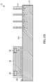
- FIGS. 1 A through 1 I illustrate the cross-sectional views of intermediate stages in the formation of a fan-out package in accordance with some embodiments.
- FIGS. 2 A through 2 I illustrate the cross-sectional views of intermediate stages in the formation of a fan-out package in accordance with some embodiments.
- FIGS. 3 A through 3 J illustrate the cross-sectional views of intermediate stages in the formation of a fan-out package in accordance with some embodiments.
- FIGS. 4 A through 4 J illustrate the cross-sectional views of intermediate stages in the formation of a fan-out package in accordance with some embodiments.
- FIGS. 5 through 10 illustrate the cross-sectional views of fan-out packages in accordance with some embodiments.
- FIG. 11 illustrates a top view of a fan-out package in accordance with some embodiments.
- FIG. 12 illustrates a process flow for forming a fan-out package in accordance with some embodiments.
- FIGS. 13 A through 13 C illustrate some top structures used for connecting the respective device dies to overlying redistribution layers in accordance with some embodiments.
- FIG. 14 illustrates an exemplary notation representing the structures shown in FIGS. 13 A through 13 C in accordance with some embodiments.
- FIGS. 15 A through 15 K illustrate the cross-sectional views of intermediate stages in the formation of a fan-out package in accordance with some embodiments.
- FIGS. 16 A and 16 B illustrate a cross-sectional view and a top view, respectively, of a fan-out package in accordance with some embodiments.
- FIGS. 17 A and 17 B illustrate a cross-sectional view and a top view, respectively, of a fan-out package in accordance with some embodiments.
- FIGS. 18 A through 18 C illustrate the cross-sectional views of fan-out packages including memory cubes in accordance with some embodiments.
- FIG. 19 illustrates a process flow for forming a fan-out package using a single molding process in accordance with some embodiments.
- first and second features are formed in direct contact
- additional features may be formed between the first and second features, such that the first and second features may not be in direct contact
- present disclosure may repeat reference numerals and/or letters in the various examples. This repetition is for the purpose of simplicity and clarity and does not in itself dictate a relationship between the various embodiments and/or configurations discussed.
- spatially relative terms such as “underlying,” “below,” “lower,” “overlying,” “upper” and the like, may be used herein for ease of description to describe one element or feature's relationship to another element(s) or feature(s) as illustrated in the figures.
- the spatially relative terms are intended to encompass different orientations of the device in use or operation in addition to the orientation depicted in the figures.
- the apparatus may be otherwise oriented (rotated 90 degrees or at other orientations) and the spatially relative descriptors used herein may likewise be interpreted accordingly.
- Integrated fan-out packages and the methods of forming the same are provided in accordance with various exemplary embodiments.
- the intermediate stages of forming the fan-out packages are illustrated. Some variations of some embodiments are discussed.
- like reference numbers are used to designate like elements.
- FIGS. 1 A through 1 I illustrate the cross-sectional views of intermediate stages in the formation of a fan-out package in accordance with some embodiments.
- the steps shown in FIGS. 1 A through 1 I are also illustrated schematically in the process flow 200 as shown in FIG. 12 .
- the process steps shown in FIGS. 1 A through 1 I are discussed referring to the process steps in FIG. 12 .
- device die 10 (which is a part of the respective wafer 2 that has a plurality of device dies) is provided.
- device die 10 is a logic die, which may be a Central Processing Unit (CPU) die, a Micro Control Unit (MCU) die, an input-output (IO) die, a BaseBand (BB) die, or an Application processor (AP) die.
- device die 10 may include a semiconductor substrate, wherein active devices such as transistors and/or diodes are formed at a top surface of the semiconductor substrate.
- metal lines and vias (not shown) are formed in an interconnect structure (not shown), which is over the semiconductor substrate, of device die 10 to interconnect the integrated circuit devices in device die 10 .
- Metal pads 12 are formed at the top surface 10 A of device die 10 .
- the top surface 10 A of device die 10 is also referred to as a front surface.
- Device die 10 has back surface 10 B, which may also be the back surface of the respective semiconductor substrate in device die 10 .
- Metal pads 12 may be aluminum pads, copper pads, aluminum copper pads, or the like.
- Metal pads 12 may be formed in a first surface region of device die 10 , and a second surface region of device die 10 has no metal pads formed therein. For example, in accordance with some exemplary embodiments as shown in FIG. 1 A , the right surface region have metal pads 12 therein, and the left surface region have no metal pads.
- FIGS. 1 B and 1 C illustrate the formation of through-vias 14 .
- the respective step is illustrated as step 202 in the process step shown in FIG. 12 .
- photo resist 16 is formed over wafer 2 , and is then patterned to form openings 15 , through which a portion of each of metal pads 12 is exposed. Through-vias 14 are then plated in openings 15 . Photo resist 16 is then removed, resulting in the structure in FIG. 1 C .
- no seed layer is formed on wafer 2 before the plating, and metal pads 12 act as the seed layer.
- a seed layer (not shown) is formed before photo resist 16 is formed, and through-vias 14 are plated on the seed layer. After the removal of photo resist 16 , the portions of the seed layer not directly underlying through-vias 14 are removed in an etching process. The remaining portions of the seed layer thus become the bottom portions of through-vias 14 .
- device die 20 is adhered to device die 10 through Die-Attach Film (DAF) 22 .
- DAF Die-Attach Film
- the respective step is illustrated as step 204 in the process step shown in FIG. 12 .
- the back surface of device die 20 is adhered to the front surface 10 A of device die 10 , and hence the corresponding die stacking is a face-to-back stacking.
- device die 20 is a memory die, which may be a Flash die, a static Random Access Memory (SRAM) die, a low power Double-Data-Rate (DDR) die, or the like.
- SRAM static Random Access Memory
- DDR Low power Double-Data-Rate
- device die 20 may be a single memory die or a stacked memory dies.
- device die 20 may also include a semiconductor substrate, wherein active devices such as transistors and/or diodes are formed at a top surface of the semiconductor substrate. Furthermore, metal lines and vias (not shown) are formed in the interconnect structure of device die 20 to interconnect the integrated circuit devices in device die 20 . The back surface of device die 20 may also be the back surface of the semiconductor substrate in device die 20 .
- FIG. 11 illustrates an exemplary top view of device die 10 and the corresponding overlying device die 20 and through-vias 14 .
- device die 20 overlaps a corner region of device die 10 , with through-vias 14 being adjacent to two sidewalls of device die 20 .
- device die 20 overlaps a center region of device die 10 , and through-vias 14 encircle device die 20 .
- Device die 20 and through-vias 14 may also be laid out using other layout schemes.
- DAF 22 is an adhesive film, and may be formed of a polymer. In accordance with some embodiments of the present disclosure, DAF 22 has a low thermal conductivity, which may be lower than about 0.5 W/m*K.
- device die 20 includes conductive pillars 28 , which may be metal pillars, formed in surface dielectric layer 26 .
- Metal pillars 28 may be formed of copper, nickel, palladium, gold, multi-layers thereof, and/or alloys thereof.
- Surface dielectric layer 26 may be formed of polybenzoxazole (PBO), polyimide, benzocyclobutene (BCB), or the like.
- Underlying metal pillars 28 may reside metal pads 24 , which may be formed of copper, aluminum, or other metals.
- encapsulating material 30 is encapsulated on device die 20 and through-vias 14 .
- the respective step is illustrated as step 206 in the process step shown in FIG. 12 .
- Encapsulating material 30 is dispensed as a fluid and then being compressed and cured, for example, in a thermal curing process.
- Encapsulating material 30 fills the gaps between device die 20 and through-vias 14 .
- Encapsulating material 30 may include a molding compound, a molding underfill, an epoxy, or a resin. After the encapsulating process, the top surface of encapsulating material 30 is higher than the top ends of metal pillars 28 and through-vias 14 .
- a planarization step such as a mechanical grinding, a Chemical Mechanical Polish (CMP) and/or a combination of both is performed to planarize encapsulating material 30 , through-vias 14 , surface dielectric layer 26 , and metal pillars 28 .
- the respective step is also illustrated as step 206 in the process step shown in FIG. 12 .
- the resulting structure is also shown in FIG. 1 E . Due to the planarization, the top surfaces of through-vias 14 are level (coplanar) with the top surfaces of metal pillars 28 , and are level (coplanar) with the top surface of encapsulating material 30 .
- dielectric layer 32 and the respective Redistribution Layers (RDLs) 34 are formed over encapsulating material 30 , through-vias 14 , and metal pillars 28 .
- the respective step is illustrated as step 208 in the process step shown in FIG. 12 .
- dielectric layers 32 are formed of a polymer(s) such as PBO, polyimide, BCB, or the like.
- RDLs 34 are formed to electrically couple to metal pillars 28 and through-vias 14 . It is noted that the illustration of RDLs 34 throughout all figures is schematic. For example, RDLs 34 are actually patterned as a plurality of discrete portions separated from each other by the respective dielectric layer(s). Each of the discrete portions of RDLs 34 is connected to the respective underlying metal pillars 28 and/or through-vias 14 . RDLs 34 may also interconnect some metal pillars 28 to the respective through-vias 14 . RDLs 34 may include metal traces (metal lines) and vias underlying and connected to the metal traces.
- RDLs 34 are formed through plating processes, wherein each of RDLs 34 includes a seed layer (not shown) and a plated metallic material over the seed layer.
- the seed layer and the plated metallic material may be formed of the same material or different materials.
- FIG. 1 G illustrates the backside grinding of device die 10 , which is grinded from its backside (the illustrated bottom side). The respective step is illustrated as step 210 in the process step shown in FIG. 12 . Accordingly, the thickness of device die 10 is reduced from thickness T 1 ( FIG. 1 F ) to thickness T 2 as shown in FIG. 1 G .
- FIG. 1 H illustrates the formation of electrical connectors 36 in accordance with some exemplary embodiments of the present disclosure.
- the respective step is illustrated as step 212 in the process step shown in FIG. 12 .
- Electrical connectors 36 are electrically coupled to RDLs 34 , metal pillars 28 , and/or through-vias 14 .
- the formation of electrical connectors 36 may include placing solder balls over RDLs 34 and then reflowing the solder balls.
- the formation of electrical connectors 36 includes performing a plating step to form solder regions over RDLs 34 , and then reflowing the solder regions.
- Electrical connectors 36 may also include metal pillars, or metal pillars and solder caps, which may also be formed through plating.
- IPD 39 may be bonded to RDLs 34 .
- IPD 39 may be used for tuning the performance of the resulting package, and may include a capacitor, for example. In accordance with alternative embodiments, no IPD 39 is bonded.
- composite wafer 38 the combined structure including device dies 10 and 20 , through-vias 14 , encapsulating material 30 , RDLs 34 , and dielectric layers 32 will be referred to as composite wafer 38 , which is a composite wafer including a plurality of device dies 10 and 20 .
- composite wafer 38 is sawed apart into a plurality of packages 40 , each including one of device dies 10 , one of device dies 20 , and the corresponding through-vias 14 .
- the respective step is illustrated as step 214 in the process step shown in FIG. 12 .
- Package 40 in accordance with some embodiments is thus formed with a single encapsulating (molding) process, although package 40 includes two levels of device dies stacked together. This is different from conventional die stacking processes, wherein two levels of device dies are encapsulated using two encapsulating processes.
- no package substrate is used in package 40 . This causes the advantageous reduction in the thickness of package 40 , and hence package 40 is suitable for mobile applications that require very thin packages.
- package 40 is a fan-out package since RDLs 34 extends beyond the edges of device die 20 , the footprint (the top-view area) of package 40 is the same as the top-view area of device die 10 , providing the top-view area of device die 10 is adequate for disposing all electrical connectors 36 . Accordingly, the top-view area of package 40 is small. In addition, the distance between metal pads 12 and electrical connectors 36 is small, resulting in the improvement in the electrical performance of the resulting package 40 .
- device die 10 which may be a logic die, often generates more heat than memory device dies such as device die 20 . Memory dies suffer from severe performance degradation from heat.
- DAF 22 which has low thermal conductivity, is used to reduce the heat generated in device die 10 from being conducted into device die 20 . Rather, the heat in device die 10 may be conducted through through-vias 14 to electrical connectors 36 . Some of through-vias 14 may also be designed as dummy vias that are not used for electrical connection between device die 10 and electrical connector 36 . The dummy through-vias 14 may be electrically floating, and are used for conducting the heat in device die 10 to electrical connectors 36 .
- FIGS. 2 A through 4 J illustrate cross-sectional views of intermediate stages in the formation of a fan-out package in accordance with some embodiments of the present disclosure.
- the materials and the formation methods of the components in these embodiments are essentially the same as the like components, which are denoted by like reference numerals in the embodiments shown in FIGS. 1 A through 1 I.
- the details regarding the formation process and the materials of the components shown in FIGS. 2 A through 4 J (and the embodiments in FIGS. 5 through 10 ) may thus be found or realized through the discussion of the embodiments shown in FIGS. 1 A through 1 H .
- FIGS. 2 A and 2 B The initial steps of some embodiments are shown in FIGS. 2 A and 2 B , which are essentially the same as the process steps shown in FIGS. 1 A through 1 C .
- Through-vias 14 are formed on metal pads 12 of device dies 10 .
- wafer 2 is sawed into individual device dies 10 .
- device die 10 is adhered to carrier 46 through adhesive film 44 .
- carrier 46 is a glass carrier.
- device die 10 there is a plurality of device dies 10 placed on carrier 46 , and device dies 10 may be laid out as an array.
- Device die 20 is then adhered to the front surface of device die 10 through DAF 22 , as shown in FIG. 2 D .
- encapsulating material 30 is dispensed to encapsulate device dies 10 and 20 .
- device die 10 is also encapsulated.
- dielectric layers 32 and RDLs 34 are formed over encapsulating material 30 , with RDLs 34 electrically coupled to metal pillars 28 and through-vias 14 .
- RDLs 34 expand beyond the edges of both device dies 10 and 20 . Accordingly, the embodiments shown in FIG. 2 F (compared to FIG. 1 F ) may be used in the embodiments in which the top-view area of device die 10 is not large enough to accommodate all of electrical connectors 36 ( FIG. 21 ), and hence RDLs 34 need to fan-out from device die 10 .
- carrier 46 is de-bonded from the overlying structure, resulting in the structure shown in FIG. 2 G .
- a backside grinding may then be performed to remove adhesive film 44 and to thin device die 10 , and the resulting structure is shown in FIG. 2 H .
- IPD 39 may be (or may not be) bonded to RDLs 34 .
- the resulting composite wafer 38 which includes device dies 10 , device dies 20 , encapsulating material 30 , through-vias 14 , RDLs 34 , and dielectric layers 32 , is sawed into individual packages 40 .
- FIGS. 3 A through 3 J illustrate the formation of fan-out packages 40 in accordance with some embodiments.
- wafer 4 is formed, which includes device dies 20 therein.
- Conductive pads (such as metal pads) 24 are formed at the front surface 20 A of device dies 20 .
- Device die 20 has back surface 20 B, which may also be the back surface of the respective semiconductor substrate (not shown) therein.
- through-vias 14 are formed, wherein the formation process may be similar to the process shown in FIGS. 1 B and 1 C . Wafer 4 is then sawed part into individual device dies 20 .
- Adhesive layer 44 may be formed of a Light-to-Heat Conversion (LTHC) material.
- DAFs 50 may be used to adhere device dies 20 to adhesive film 44 .
- the distance between device dies 20 - 1 and 20 - 2 is selected, so that the space between the through-vias 14 over device die 20 - 1 and the through-vias 14 over device die 20 - 2 is big enough to accommodate device die 10 ( FIG. 3 D ).
- device dies 20 - 1 and 20 - 2 are identical to each other, and device die 20 - 1 is rotated by 180 degrees (in a top view) relative to device die 20 - 2 .
- device dies 20 - 1 and 20 - 2 are partially identical to each other, wherein the lower part (of device die 20 - 1 ) 20 - 1 -L such as the active devices and the interconnect structure (not shown) is identical to the lower part 20 - 2 -L of device die 20 - 2 .
- the upper parts 20 - 1 -U and 20 - 2 -U which include the top redistribution layer(s) (not shown), however, are different from each other, so that the conductive pads 24 in device die 20 - 1 are concentrated on the left side of device die 20 - 1 , and the conductive pads 24 in device die 20 - 2 are concentrated on the right side of device die 20 - 2 .
- device dies 20 - 1 and 20 - 2 are different types of dies, and have different structures.
- device dies 20 may include more than two dies, such as four dies, and device die 10 may include more than one die, such as two dies, for the integration of multiple logics and multiple memory chips depending on design needs.
- device dies 20 may include multi-chips stacked cube structure in each individual device dies 20 - 1 , 20 - 2 (not shown). Each stacked cube structure may contain such a plurality of chips such as 2-chips to 9-chips. In each stacked cube structure, each of the stacked chips may be a homogeneous functional chip such as a memory functional chip and/or a heterogeneous functional chip such as a logic functional controller chip.
- the stacked chips may also be multiple homogeneous memory chips (not shown).
- the stacked chips may have Through-Silicon Vias (also known as Through-Substrate Vias, or TSVs), depending on the design needs, such as a high bandwidth memory (HBM) cube.
- TSVs Through-Silicon Vias
- HBM high bandwidth memory
- device die 10 is placed over device dies 20 , and is adhered to the front surfaces of device dies 20 through DAF 22 . A portion of device die 10 also overlaps the gap between device dies 20 .
- device die 10 includes metal pillars 52 over metal pads 12 , with no dielectric layer encircling metal pillars 52 .
- no metal pillars are formed over metal pads 12 , and metal pads 12 are the top conductive features of device die 10 .
- FIG. 3 E illustrates the encapsulation of device dies 10 and 20 and through-vias 14 in encapsulating material 30 , followed by a mechanical grinding, a Chemical Mechanical Polish (CMP) and/or a combination of both to expose metal pillars 52 and through-vias 14 .
- CMP Chemical Mechanical Polish
- dielectric layers 32 and RDLs 34 are formed, and RDLs 34 are electrically coupled to metal pillars 52 and through-vias 14 , as shown in FIG. 3 F .
- device die 41 may be optionally bonded to RDLs 34 ( FIG. 3 G ), and electrical connectors 36 are formed to connect to RDLs 34 ( FIG. 3 H ).
- Device die 41 may include through-vias (sometimes referred to as through-silicon vias or through-substrate vias) penetrating through the semiconductor substrate in device die 41 .
- An IPD may also be bonded to RDLs 34 in accordance with some embodiments.
- Electrical connectors 36 may include a solder ball grid array for bonding to a Printed Circuit Board (PCB).
- Electrical connectors 36 may also be a flip chip bump such as C 4 solder bump, copper pillar bump, and the like for bonding to a package substrate (not shown). This configuration may apply to all embodiments throughout the present disclosure.
- Carrier 46 is then de-bonded from the overlying structure, and the resulting structure is shown in FIG. 31 .
- device dies 20 - 1 and 20 - 2 are grinded from the backside, and DAFs 50 are removed through grinding.
- the resulting structure is shown in FIG. 3 J .
- FIG. 3 J further illustrates the attachment of lid 54 to device dies 20 , for example, through Thermal Interface Material (TIM) 56 .
- TIM 56 has thermal conductivity higher than the thermal conductivity of DAFs 22 ( FIGS. 1 I, 21 , and 3 J).
- the thermal conductivity of TIM 56 may be higher than about 1 W/m * K or even higher.
- Lid 54 may be formed of a material having good thermal conductivity.
- lid 54 includes a metal such as aluminum, copper, an aluminum/copper alloy, stainless steel, or the like.
- FIGS. 4 A through 4 J illustrate the formation of package 40 ( FIG. 4 J ) in accordance with some embodiments. These embodiments are essentially the same as the embodiments shown in FIGS. 3 A through 3 J , except device die 10 does not have the metal pillars 52 ( FIG. 3 J ) that are formed over metal pads 12 . A brief discussion of the formation process is provided below. The details of these embodiments may be found in the embodiments in FIGS. 3 A through 3 J , and are not repeated herein.
- FIGS. 4 A through 4 C are essentially the same as the steps shown in FIGS. 3 A through 3 C .
- device die 10 is adhered to device dies 20 (including 20 - 1 and 20 - 2 ).
- Device die 10 includes metal pads 12 as the top surface conductive features, and no metal pillars are formed over metal pads 12 .
- Device 10 is also placed between the through-vias 14 directly over device die 20 - 1 and the through-vias 14 directly over device die 20 - 2 .
- FIG. 4 E illustrates the direct formation of encapsulating material 30 while exposing metal pads 12 and through-vias 14 without planarization.
- the process steps shown in FIGS. 4 F through 4 J are essentially the same as the process steps shown in FIGS. 3 F through 3 J , and the details are not repeated herein.
- FIGS. 5 through 10 illustrate the packages formed in accordance with some embodiments of the present disclosure.
- the formation process may be understood from the embodiments in FIGS. 1 A through 4 J .
- the package 40 shown in FIG. 5 is similar to the package shown in FIG. 1 I , except in FIG. 5 , no metal pillars are formed, and metal pads 24 are the top conductive features of die 20 .
- RDLs 34 include vias that are in physical contact with metal pads 24 .
- the package 40 shown in FIG. 6 is similar to the package shown in FIG. 2 I , except in FIG. 6 , no metal pillars are formed, and metal pads 24 are the top conductive features of die 20 .
- RDLs 34 include vias that are in physical contact with metal pads 24 .
- FIG. 7 illustrates package 40 , which is similar to the package 40 in FIG. 2 I , except device die 20 is partially offset from device die 10 .
- a first portion of device die 20 overlaps a portion of encapsulating material 30 , and does not overlap any portion of device die 10 .
- a second portion of device die 20 overlaps a portion of device die 10 .
- the first portion of device die 20 is thus suspended with no underlying support of device die 10 .
- the partial offset of device die 20 relative to device die 10 advantageously reduces the overlap area of device dies 10 and 20 . Accordingly, an increased percentage of the top surface area of device die 10 can be used for forming metal pads 12 and through-vias 14 , rather than being overlapped by device die 20 .
- the offset of device die 20 from device die 10 does not result in the undesirable increase in the form factor (the top-view area) of package 40 in accordance with some embodiments.
- the top-view area of package 40 is determined by the area required to fit all electrical connectors 36 , as long as the total footprint area of device dies 10 and 20 does not exceed the area required to fit all electrical connectors 36 , the partial offset of device die 20 from device die 10 will not cause the increase in the form factor (the top view area).
- FIG. 8 illustrates package 40 similar to what is shown in FIG. 7 , except no metal pillars are formed over metal pads 24 .
- FIG. 9 illustrates package 40 in accordance with some embodiments, wherein there are two device dies 10 and two device dies 20 partially offset from the respective device dies 10 .
- Each device die 10 has a first portion overlapping a portion of a respective underlying device die 20 , and a second portion offset from the respective underlying device die 20 .
- Through-vias 14 are formed directly on metal pads 24 of each of device dies 20 .
- FIG. 10 illustrates package 40 in accordance with some embodiments, wherein there are four device dies 20 (including 20 - 3 and 20 - 4 ), and one device die 10 .
- the four device dies 20 includes two higher-level device dies 20 - 4 , and two lower-level device dies 20 - 3 underlying the higher-level device dies 20 - 4 .
- Each of the higher-level device dies 20 - 4 has a first portion overlapping a portion of the respective underlying lower-level device die 20 - 3 , and a second portion offset from the respective underlying lower-level device die 20 - 3 .
- Four device dies 20 are encapsulated in a first encapsulating material 30 A in a first encapsulating process.
- Device die 10 is over higher-level device dies 20 - 4 , and is encapsulated in a second encapsulating material 30 B in a second encapsulating process.
- Device die 10 is partially offset from both higher-level device dies 20 - 4 .
- device die 10 has first portions overlapping portions of higher-level device die 20 - 4 , and a second portion overlapping the gap between higher-level device die 20 - 4 .
- Encapsulating materials 30 A and 30 B may be the same as each other or different from each other.
- Through-vias 14 A are formed directly on metal pads 24 A of lower-level device dies 20 - 3 .
- Some of through-vias 14 B are formed directly on metal pads 24 B of higher-level device dies 20 - 4 .
- the interface of encapsulating materials 30 A and 30 B may be distinguishable from each other due to the CMP performed on the top surface of encapsulating material 30 A, which causes some of the sphere-shaped fillers 58 in encapsulating material 30 A to be grinded to have planar (rather than spherical) top surfaces.
- each of through-vias 14 A and 14 B may have a top width greater than the respective bottom width.
- the transition of through-vias 14 B to the respective underlying through-vias 14 A will also show discontinuity, and the top widths of through-vias 14 A may be greater than the bottom widths of the respective overlying through-vias 14 B.
- the partial offset of higher-level die(s) from the lower-level dies results in the advantageous increase in the surface area of the lower-level dies 20 - 3 that can be used for forming metal pads and through-vias.
- the lower-level dies 20 - 3 occupy the majority top-view area of package 40 , the warpage of package 40 is not severe.
- FIGS. 13 A, 13 B, and 13 C illustrate the structures of top conductive features in device dies in accordance with some embodiments of the present disclosure.
- device die S 1 is illustrated.
- device die S 1 is a logic die, which may be a GPU die, a CPU die, a GPU-CPU combo function die, a MCU die, an IO die, a BB die, or an AP die.
- device die S 1 may include a semiconductor substrate, which may be a silicon substrate in accordance with some embodiments, wherein active devices (not shown) such as transistors and/or diodes are formed at a top surface of the semiconductor substrate.
- active devices such as transistors and/or diodes
- metal lines and vias are formed in an interconnect structure (not shown), which is over the semiconductor substrate to interconnect the integrated circuit devices in device die S 1 .
- Metal pads 104 are formed in device die S 1 .
- metal pads 104 are aluminum pads, which may also include some copper therein.
- Metal pads 104 are electrically coupled to the integrated circuit devices such as active devices in device die S 1 .
- Passivation layer 106 is formed to have some portions covering the edge portions of metal pads 104 . The central portions of metal pads 104 are exposed through the openings in passivation layer 106 .
- Passivation layer 106 may be a single layer or a composite layer, and may be formed of a non-porous material. In accordance with some embodiments of the present disclosure, passivation layer 106 is a composite layer comprising a silicon oxide layer (not shown), and a silicon nitride layer (not shown) over the silicon oxide layer. Passivation layer 106 may also be formed of other non-porous dielectric materials such as Un-doped Silicate Glass (USG), silicon oxynitride, and/or the like.
- USG Un-doped Silicate Glass
- Dielectric layer 108 is formed over passivation layer 106 .
- Dielectric layer 108 may be a polymer layer formed of a polymer such as polyimide, PBO, BCB, or the like. The formation methods may include spin coating, for example.
- Dielectric layer 108 may be dispensed in a liquid form, and then cured.
- Over dielectric layer 108 may reside dielectric layer 110 , which may be formed of a material selected from the same candidate materials for forming dielectric layer 108 , which may include polyimide, PBO, BCB, or the like.
- dielectric layers 108 and 110 are formed of different materials.
- dielectric material 108 may be formed of polyimide
- dielectric layer 110 may be formed of PBO.
- Conductive posts 112 are formed over and connected to metal pads 104 . Conductive posts 112 are sometimes referred to as metal pillars or metal posts. In accordance with some embodiments, conductive posts 112 are formed of metallic materials such as copper, nickel, gold, alloys thereof, or multi-layers thereof. Conductive posts 112 extend into dielectric layers 106 , 108 , and 110 . In accordance with some embodiments, the top surface of dielectric layer 110 is coplanar with the top surfaces of metal posts 112 . In accordance with other embodiments, dielectric layer 110 includes portions covering metal posts 112 . The portions of dielectric layer 110 covering metal posts 112 may be removed in the grinding process after device die S 1 is molded, as will be discussed in subsequent processes.
- FIG. 13 B schematically illustrates the structures of the top conductive features in device die S 1 in accordance with alternative embodiments.
- the top features of device die S 1 include metal pads 104 and passivation layer 106 , wherein the center portions of metal pads 104 are exposed. No metal posts are formed over metal pads 104 . Rather, the subsequent formed RDLs are directly connected to metal pads 104 .
- FIG. 13 C schematically illustrates the structures of the top conductive features in device die S 1 in accordance with alternative embodiments.
- Device die S 1 in accordance with these embodiments are similar to that is shown in FIG. 13 A , except dielectric layer 110 in FIG. 13 A is omitted in FIG. 13 C .
- dielectric layer 108 which is the top dielectric layer in device die S 1 , has a top surface lower than the top surfaces of metal posts 112 .
- FIG. 14 illustrates a symbolic view of device die S 1 .
- the illustrated device die S 1 may actually have the structure as shown in any of FIGS. 13 A, 13 B , or 13 C.
- the illustrated conductive features 114 in device die S 1 may represent the metal posts 112 in FIG. 13 A or 13 C , or the metal pads 114 in FIG. 13 B .
- the illustrated dielectric layer 116 in FIG. 14 may represent dielectric layers 106 , 108 , and 110 in FIG. 13 A , dielectric layer 106 in FIG. 13 B , or dielectric layers 106 and 108 in FIG. 13 C .
- FIGS. 15 A through 15 J illustrate the cross-sectional views of intermediate stages in the formation of a fan-out package in accordance with some embodiments.
- wafer 120 is formed.
- Wafer 120 includes a plurality of device dies M 1 therein.
- device dies M 1 are logic dies including logic circuits, memory dies, analog dies, sensor dies, or the like.
- device dies M 1 may be Flash memory dies, SRAM memory dies, low power DDR dies, or the like.
- device dies M 1 may include semiconductor substrates, wherein active devices such as transistors and/or diodes are formed at the top surfaces of the semiconductor substrates. Furthermore, metal lines and vias (not shown) are formed in the interconnect structures of device dies M 1 to interconnect the integrated circuit devices in the respective device dies M 1 .
- the back surfaces of device dies M 1 may also be the back surfaces of the semiconductor substrates in the respective device dies M 1 . Furthermore, the back surfaces of device dies M 1 are adhered to DAFs 22 .
- Metal pads 122 are formed at the top surfaces (front surfaces) of device dies M 1 .
- Metal pads 122 may be aluminum pads, copper pads, aluminum copper pads, or the like. In each of device dies M 1 , metal pads 122 may be offset from the centers of the respective device dies M 1 .
- metal pads 122 may be formed in the illustrated left sides of the respective device dies M 1 , and the right sides of device dies M 1 have no metal pads formed therein.
- Through-vias 124 are formed on the top surfaces of device dies M 1 .
- the respective step is illustrated as step 302 in the process flow 300 shown in FIG. 19 .
- through-vias 124 are formed using similar methods as illustrated in FIGS. 1 B and 1 C .
- the material of through-vias 124 may be selected from the same candidate materials for forming through-vias 14 in FIG. 1 C . The details are thus not repeated herein. Since Through-vias 124 are formed in a single formation process (such as plating), with each for through-vias 124 formed in a single opening (similar to opening 15 in FIG. 1 B ), there is no visible interface between the upper portions and the respective lower portions of through-vias 124 .
- each of through-vias 124 may be substantially straight, with no abrupt changes in the tilt angle of the edges.
- the side profile of through-vias 124 may be vertical and/or tapered, and the top view cross-section shape of through-vias 124 may be circular and/or non-circular such as oval, hexagon, octagon, and the like.
- the features discussed for through-vias 124 may apply to all other through-vias through out the present disclosure.
- through-vias 124 are formed directly on metal pads 122 . Accordingly, seed layer may be or may not be used in the formation of through-vias 124 , and the materials of through-vias 124 are homogenous.
- RDLs may be formed close to the top surfaces of device dies M 1 , wherein the RDLs are used to reroute electrical connections, for example, to the left sides of the respective device dies M 1 .
- Through-vias 124 are then formed on the top of the RDLs. In a subsequent step, device dies M 1 are singulated from wafer 120 as discrete device dies.
- FIG. 15 B illustrates the formation of wafer 128 , which includes device dies M 2 therein.
- device dies M 1 and M 2 are same type of device dies.
- device dies M 1 and M 2 may both be SRAM dies.
- device dies M 1 and M 2 may have identical structures in the bottom parts.
- the structures and the layouts of device dies M 1 and M 2 including low-k dielectric layers (not shown), the metal lines and vias (not shown) in the low-k dielectric layers, the transistors and memory devices (not shown) may be identical to each other.
- the top routing portions of device dies M 1 may be different from that of device dies M 2 , so that the electrical connections of device dies M 2 are routed to the right sides of the respective device dies M 2 , which is opposite to device dies M 1 .
- the backsides of device dies M 2 may also be adhered to DAFs 22 .
- Device dies M 2 also have metal pads 122 formed therein. Through-vias 124 are formed over metal pads 122 , for example, through plating. The respective step is illustrated as step 304 in the process flow 300 shown in FIG. 19 . The materials and the formation process of metal pads 122 and through-vias 124 may be found referring to the discussion of FIG. 15 A , and hence are not repeated herein.
- Device dies M 2 are then singulated from wafer 128 as discrete device dies.
- Wafer 130 includes a plurality of device dies M 3 therein.
- device dies M 3 are logic dies including logic circuits, memory dies, analog dies, sensor dies, or the like.
- device dies M 3 may be Flash memory dies, SRAM memory dies, low power DDR dies, or the like.
- device dies M 3 may have structures the same as or different from that of device dies M 1 and/or M 2 .
- Metal pads 132 are formed at the top surfaces (front surfaces) of device dies M 3 , and may be aluminum pads, copper pads, aluminum copper pads, or the like. Similar to device dies M 1 , metal pads 132 may also be offset from the center of the respective device dies M 3 . For example, metal pads 132 may be formed in the illustrated left sides of the respective device dies M 3 , and the right sides of device dies M 3 have no metal pads formed therein.
- Through-vias 134 are formed on the top surfaces of device dies M 3 , and may be formed using similar methods (and similar materials) as illustrated in FIGS. 1 B and 1 C . The respective step is illustrated as step 306 in the process flow 300 shown in FIG. 19 .
- through-vias 134 are formed directly on metal pads 132 . Accordingly, seed layer may be or may not be used in the formation of through-vias 134 .
- RDLs (not shown) are formed close to the top surfaces of device dies M 3 , wherein the RDLs are used to reroute electrical connections, for example, to the left sides of the respective device dies M 3 . Through-vias 134 may then be formed over the rerouting RDLs.
- Device dies M 3 are singulated from wafer 130 as discrete device dies.
- FIG. 15 D illustrates the formation of wafer 138 , which includes device dies M 4 therein.
- device dies M 3 and M 4 are the same type of device dies. Furthermore, the relationship between device dies M 3 and M 4 may be similar to the relationship between device dies M 1 and M 2 . The backsides of device dies M 4 may also be adhered to DAFs 22 .
- Device dies M 4 also have metal pads 132 formed therein. Through-vias 134 are formed on metal pads 132 . The respective step is illustrated as step 308 in the process flow 300 shown in FIG. 19 . The materials and the formation process of metal pads 132 and through-vias 134 may be found referring to the discussion of FIG. 15 A , and hence are not repeated herein.
- Device dies M 4 are then singulated from wafer 138 as discrete device dies.
- step 310 in the process flow 300 shown in FIG. 19 .
- Device die M 1 is placed on the left side of device die M 2 , and the through-vias 124 in device die M 1 is further on the left side of device die M 1 .
- the through-vias 124 in device die M 2 is further on the right side of device die M 2 .
- Device dies M 1 and M 2 are spaced apart from each other by distance D 1 .
- device dies M 3 and M 4 are picked and placed, and are adhered to the front sides of device dies M 1 and M 2 , respectively, through DAFs 22 .
- the respective step is illustrated as step 312 in the process flow 300 shown in FIG. 19 .
- device die M 3 overlaps the right portion of the respective underlying device die M 1 , and may or may not overlap the center of device die M 1 .
- through-vias 134 of device die M 3 are on the left side of the respective device die M 3 .
- Device die M 4 overlaps the left portion of the respective underlying device die M 2 , and may or may not overlap the center of device die M 2 .
- through-vias 134 of device die M 4 are on the right side of the respective device die M 4 .
- device die M 3 has a right portion extending beyond the right edge of device die M 1 . Accordingly, the right portion of device die M 3 overhangs. In accordance with alternative embodiments of the present disclosure, an entirety of device die M 3 overlaps device die M 1 with no overhang.
- Device die M 4 may have a left portion extending beyond the left edge of device die M 2 . Accordingly, the left portion of device die M 4 overhangs. In accordance with alternative embodiments of the present disclosure, an entirety of device die M 4 overlaps device die M 2 with no overhang.
- Device dies M 3 and M 4 have distance D 2 , which may be smaller than, equal to, or greater than, distance D 1 between device dies M 1 and M 2 .
- device die S 1 is picked and placed over device dies M 3 and M 4 , and is adhered to the front surfaces of both device dies M 3 and M 4 through DAF 22 .
- the respective step is illustrated as step 314 in the process flow 300 shown in FIG. 19 .
- a portion of device die S 1 also overlaps the gap between device dies M 3 and M 4 .
- device die S 1 includes conductive features 114 and surface dielectric layer 116 , which represent the features shown in FIGS. 13 A, 13 B , or 13 C.
- the top surfaces of through-vias 124 and 134 are higher than, lower than, or level with the top surfaces of device die S 1 .
- FIG. 15 H illustrates the encapsulation of device dies M 1 , M 2 , M 3 , M 4 , S 1 and through-vias 124 and 134 in encapsulating material 30 , followed by a mechanical grinding, a CMP and/or a combination of both to expose conductive features 114 and through-vias 124 and 134 .
- the respective step is illustrated as step 316 in the process flow 300 shown in FIG. 19 . Since device dies M 1 , M 2 , M 3 , M 4 , S 1 and through-vias 124 and 134 are encapsulated through a single encapsulation process, there is no distinguishable interface (such as horizontal interface) in encapsulating material 30 .
- the fillers in encapsulating material 30 which fillers may include spherical particles (such as A 1 2 O 3 particles), will remain to be spherical.
- the spherical particles that are ground in the planarization of encapsulating material 30 will have upper portions removed during the grinding process, and bottom portions remaining to have planar top surfaces and rounded bottom surfaces.
- each of device dies M 3 , M 4 , and S 1 may include a first portion overlapping the respective underlying dies M 1 /M 2 , and M 3 /M 4 , respectively, and a second portion overlapping encapsulating material 30 .
- the second portion may not have any device die directly underlying it.
- the height of through-vias of device dies M 3 and M 4 is smaller than that of device dies M 1 and M 2 due to stacking.
- dielectric layers 32 and RDLs 34 are formed, and RDLs 34 are electrically coupled to conductive features 114 and through-vias 124 and 134 , as shown in FIG. 151 .
- the respective step is illustrated as step 318 in the process flow 300 shown in FIG. 19 .
- device die C 1 may be optionally bonded to RDLs 34 ( FIG. 15 J ), for example, through flip-chip bonding, hybrid bonding, or surface mounting.
- Device die C 1 may be an Integrated Passive Device (IPD), a memory die, an Application Specific Integrated Circuit (ASIC) die, or the like.
- IPD Integrated Passive Device
- ASIC Application Specific Integrated Circuit
- Device die C 1 may include through-vias (sometimes referred to as through-silicon vias or through-substrate vias) penetrating through the semiconductor substrate in device die C 1 .
- An IPD may also be bonded to RDLs 34 in accordance with some embodiments.
- electrical connectors 36 are formed to connect to RDLs 34 .
- the respective step is illustrated as step 320 in the process flow 300 shown in FIG. 19 .
- Heat dissipating lid 54 is attached to the resulting package, for example, through TIM 56 .
- the respective step is illustrated as step 322 in the process flow 300 shown in FIG. 19 .
- Heat dissipating lid 54 may be formed of a material having good thermal conductivity.
- heat dissipating lid 54 includes a metal such as aluminum, copper, an aluminum/copper alloy, stainless steel, or the like.
- Package 40 is thus formed.
- FIGS. 16 A and 16 B illustrate a cross-sectional view and a top view, respectively, of multi-level fan-out package 40 in accordance with some embodiments.
- FIGS. 16 A and 16 B are similar to the embodiments in FIG. 15 K , except that device dies M 3 and M 4 are laid out differently than in FIG. 15 K .
- the formation process of the package 40 shown in FIGS. 16 A and 16 B is essentially the same as shown in FIGS. 15 A through 15 K , and hence is not repeated herein.
- FIG. 16 B a first straight line 140 interconnecting the centers of device dies M 1 and M 2 is in the X-direction.
- a second straight line 142 interconnecting the centers of device dies M 3 and M 4 is in the Y-direction. Accordingly, the aligning directions of device dies M 1 and M 2 is perpendicular to the aligning direction of device dies M 3 and M 4 .
- An advantageous feature of this layout is that there are smaller portions of devices M 3 and M 4 overlapping device dies M 1 and M 2 , which yields more surfaces areas of device dies M 1 and M 2 for forming through-vias 124 . Also such configuration may lead to symmetric package layout for better warpage control and mechanical reliability/stability.
- FIG. 16 A illustrates a cross-sectional view of package 40 , wherein the cross-sectional view is obtained from the line containing 16 A- 16 A in FIG. 16 B .
- a first straight line (not shown) interconnecting the centers of device dies M 1 and M 2 may be parallel to a second straight line (not shown) interconnecting the centers of device dies M 1 and M 2 .
- FIGS. 17 A and 17 B illustrate a cross-sectional view and a top view, respectively, of multi-level fan-out package 40 in accordance with some embodiments. These embodiments are similar to the embodiments in FIGS. 16 A and 16 B , except that additional device dies S 2 and/or S 3 are placed overlapping device dies M 3 and M 4 , respectively.
- the formation process of the package 40 shown in FIGS. 17 A and 17 B is essentially the same as shown in FIGS. 15 A through 15 K , and hence is not repeated herein.
- Each of device dies S 2 and S 3 may be a logic die, a memory die, an IPD, or the like.
- the top conductive features of device dies S 2 and S 3 may be selected from any of the structures shown in FIGS. 13 A, 13 B, and 13 C .
- FIGS. 18 A, 18 B, and 18 C illustrate fan-out packages 40 in accordance with some embodiments. These embodiments are similar to the embodiments shown in FIG. 1 I , except device die 20 in FIG. 1 I is replaced with device cubes 144 in FIGS. 18 A, 18 B, and 18 C .
- through-vias 14 are distributed on the opposite sides of device cube 144 .
- through-vias 14 are distributed on one side (the illustrated right side, for example), but not on the opposite side, of device cube 144 .
- FIGS. 18 A and 18 B and entirety of device cube 144 overlaps device die S 1 .
- FIG. 18 A and 18 B illustrate fan-out packages 40 in accordance with some embodiments. These embodiments are similar to the embodiments shown in FIG. 1 I , except device die 20 in FIG. 1 I is replaced with device cubes 144 in FIGS. 18 A, 18 B, and 18 C .
- through-vias 14 are distributed on the opposite sides of device cube 144 .
- through-vias 14 are distributed on one side (the illustrated right side, for example), but not on the opposite side, of device cube 144 . Furthermore, as shown in FIG. 18 C , device cube 144 extends beyond the left edge of device die S 1 to overlap encapsulating material 30 , and hence yielding more space for forming metal pads 12 and through-vias 14 .
- each of device cubes 144 includes a plurality of device dies MC 1 , which may be memory dies in accordance with some embodiments.
- Device dies MC 1 may have identical or different structures, with through-vias (not shown) penetrating through the semiconductor substrates therein.
- the top conductive features of memory cubes 144 may also adopt any structure shown in FIGS. 13 A, 13 B , and 13 C.
- Device cube 144 may include stacked multi-chips such as 2-chips to 9-chips.
- all stacked chips may be homogeneous functional chips such as a memory function chip and/or heterogeneous functional chips such as a logic functional controller chip and multiple homogeneous memory chips (not shown).
- the stacked chips may have through-silicon vias (TSVs) depending the design needs, and may form, for example a high bandwidth memory (HBM) cube.
- TSVs through-silicon vias
- the embodiments of the present disclosure have some advantageous features.
- package substrate is not used, and the resulting package is thin.
- the thermal decoupling of the logic die and memory die by using DAF prevents the memory die from the performance degradation caused by the heat generated in the logic die.
- the top-view area of the package is minimized.
- a higher-level die and a lower-level die may be encapsulated by a same encapsulation process, and hence the cost and the warpage of the package are reduced.
- a method includes forming a first through-via from a first conductive pad of a first device die, and forming a second through-via from a second conductive pad of a second device die.
- the first and the second conductive pads are at top surfaces of the first and the second device dies, respectively.
- the first and the second conductive pads are used as seed layers.
- the second device die is adhered to the top surface of the first device die.
- the method further includes encapsulating the first and the second device dies and the first and the second through-vias in an encapsulating material, with the first and the second device dies and the first and the second through-vias encapsulated in a same encapsulating process.
- the encapsulating material is planarized to reveal the first and the second through-vias. Redistribution lines are formed to electrically couple to the first and the second through-vias.
- a method includes forming a first through-via on a first conductive pad of a first device die, forming a second through-via on a second conductive pad of a second device die, placing the first device die and the second device die over a carrier, forming a third through-via on a third conductive pad of a third device die, and forming a fourth through-via on a fourth conductive pad of a fourth device die.
- the method further includes adhering the third device die and the fourth device die to top surfaces of the first device die and second device die, respectively, and simultaneously encapsulating the first, the second, the third, and the fourth device dies and the first, the second, the third, and the fourth through-vias in an encapsulating material.
- the encapsulating material is planarized to reveal the first, the second, the third, and the fourth through-vias. Redistribution lines are formed over and electrically coupling to the first, the second, the third, and the fourth through-vias.
- a method includes placing a first device die and a second device die over a carrier, wherein the first device die includes a first through-via, and the second device die includes a second through-via.
- a third device die is placed over the first device die.
- the third device die includes a first portion overlapping a gap between the first device die and the second device die, a second portion overlapping a portion of the first device die, and a third through-via higher than the first portion of the third device die.
- the first, the second, and the third device dies and the first, the second, and the third through-vias are encapsulated in an encapsulating material.
- the encapsulating material is planarized to reveal the first through-via, the second through-via, and the third through-via. Redistribution lines are formed over and electrically coupling to the first through-via, the second through-via, and the third through-via.
- a package includes a first device die, a first through-via having a first bottom surface contacting a top surface of a first conductive pad of the first device die, a second device die having a portion overlapping a portion of the first device die, and a second through-via.
- the second through-via includes a lower portion at a same level as the first device die, and an upper portion at a same level as the second device die.
- the lower portion has a second bottom surface contacting a top surface of a second conductive pad of the second device die.
- a top surface of the upper portion is coplanar with a top surface of the first through-via, and the lower portion is continuously connected to the upper portion with no distinguishable interface therebetween.
- the package further includes an encapsulating material encapsulating the first device die, the second device die, the first through-via, and the second through-via therein, and redistribution lines over and electrically coupling to the first through-via and the second through-via.
Abstract
Description
Claims (20)
Priority Applications (2)
| Application Number | Priority Date | Filing Date | Title |
|---|---|---|---|
| US16/418,298 US11532594B2 (en) | 2015-09-21 | 2019-05-21 | Integrated fan-out package and the methods of manufacturing |
| US18/064,713 US20230114652A1 (en) | 2016-04-15 | 2022-12-12 | Integrated Fan-Out Package and the Methods of Manufacturing |
Applications Claiming Priority (6)
| Application Number | Priority Date | Filing Date | Title |
|---|---|---|---|
| US201562221443P | 2015-09-21 | 2015-09-21 | |
| US15/004,240 US10049953B2 (en) | 2015-09-21 | 2016-01-22 | Method of manufacturing an integrated fan-out package having fan-out redistribution layer (RDL) to accommodate electrical connectors |
| US15/130,211 US9917072B2 (en) | 2015-09-21 | 2016-04-15 | Method of manufacturing an integrated stacked package with a fan-out redistribution layer (RDL) and a same encapsulating process |
| US15/912,039 US10128213B2 (en) | 2015-09-21 | 2018-03-05 | Integrated fan-out stacked package with fan-out redistribution layer (RDL) |
| US16/180,214 US11538788B2 (en) | 2015-09-21 | 2018-11-05 | Integrated fan-out stacked package with fan-out redistribution layer (RDL) |
| US16/418,298 US11532594B2 (en) | 2015-09-21 | 2019-05-21 | Integrated fan-out package and the methods of manufacturing |
Related Parent Applications (1)
| Application Number | Title | Priority Date | Filing Date |
|---|---|---|---|
| US16/180,214 Continuation US11538788B2 (en) | 2015-09-21 | 2018-11-05 | Integrated fan-out stacked package with fan-out redistribution layer (RDL) |
Related Child Applications (1)
| Application Number | Title | Priority Date | Filing Date |
|---|---|---|---|
| US18/064,713 Continuation US20230114652A1 (en) | 2016-04-15 | 2022-12-12 | Integrated Fan-Out Package and the Methods of Manufacturing |
Publications (2)
| Publication Number | Publication Date |
|---|---|
| US20190273064A1 US20190273064A1 (en) | 2019-09-05 |
| US11532594B2 true US11532594B2 (en) | 2022-12-20 |
Family
ID=58283255
Family Applications (4)
| Application Number | Title | Priority Date | Filing Date |
|---|---|---|---|
| US15/130,211 Active US9917072B2 (en) | 2015-09-21 | 2016-04-15 | Method of manufacturing an integrated stacked package with a fan-out redistribution layer (RDL) and a same encapsulating process |
| US15/912,039 Active US10128213B2 (en) | 2015-09-21 | 2018-03-05 | Integrated fan-out stacked package with fan-out redistribution layer (RDL) |
| US16/180,214 Active 2036-04-16 US11538788B2 (en) | 2015-09-21 | 2018-11-05 | Integrated fan-out stacked package with fan-out redistribution layer (RDL) |
| US16/418,298 Active 2036-06-10 US11532594B2 (en) | 2015-09-21 | 2019-05-21 | Integrated fan-out package and the methods of manufacturing |
Family Applications Before (3)
| Application Number | Title | Priority Date | Filing Date |
|---|---|---|---|
| US15/130,211 Active US9917072B2 (en) | 2015-09-21 | 2016-04-15 | Method of manufacturing an integrated stacked package with a fan-out redistribution layer (RDL) and a same encapsulating process |
| US15/912,039 Active US10128213B2 (en) | 2015-09-21 | 2018-03-05 | Integrated fan-out stacked package with fan-out redistribution layer (RDL) |
| US16/180,214 Active 2036-04-16 US11538788B2 (en) | 2015-09-21 | 2018-11-05 | Integrated fan-out stacked package with fan-out redistribution layer (RDL) |
Country Status (1)
| Country | Link |
|---|---|
| US (4) | US9917072B2 (en) |
Families Citing this family (43)
| Publication number | Priority date | Publication date | Assignee | Title |
|---|---|---|---|---|
| US9917072B2 (en) | 2015-09-21 | 2018-03-13 | Taiwan Semiconductor Manufacturing Company, Ltd. | Method of manufacturing an integrated stacked package with a fan-out redistribution layer (RDL) and a same encapsulating process |
| US10049953B2 (en) | 2015-09-21 | 2018-08-14 | Taiwan Semiconductor Manufacturing Company, Ltd. | Method of manufacturing an integrated fan-out package having fan-out redistribution layer (RDL) to accommodate electrical connectors |
| US9935080B2 (en) | 2016-04-29 | 2018-04-03 | Taiwan Semiconductor Manufacturing Company, Ltd. | Three-layer Package-on-Package structure and method forming same |
| US10204884B2 (en) * | 2016-06-29 | 2019-02-12 | Intel Corporation | Multichip packaging for dice of different sizes |
| US9825007B1 (en) * | 2016-07-13 | 2017-11-21 | Taiwan Semiconductor Manufacturing Co., Ltd. | Chip package structure with molding layer and method for forming the same |
| US11469215B2 (en) * | 2016-07-13 | 2022-10-11 | Taiwan Semiconductor Manufacturing Co., Ltd. | Chip package structure with molding layer and method for forming the same |
| KR101973431B1 (en) * | 2016-09-29 | 2019-04-29 | 삼성전기주식회사 | Fan-out semiconductor package |
| WO2018063413A1 (en) * | 2016-10-01 | 2018-04-05 | Intel Corporation | Electronic device package |
| US10475770B2 (en) | 2017-02-28 | 2019-11-12 | Amkor Technology, Inc. | Semiconductor device having stacked dies and stacked pillars and method of manufacturing thereof |
| CN107123645A (en) * | 2017-05-11 | 2017-09-01 | 王家恒 | Fan-out-type integrated encapsulation structure and preparation method thereof, terminal device |
| US10217720B2 (en) * | 2017-06-15 | 2019-02-26 | Invensas Corporation | Multi-chip modules formed using wafer-level processing of a reconstitute wafer |
| JP2019054160A (en) * | 2017-09-15 | 2019-04-04 | 東芝メモリ株式会社 | Semiconductor device |
| JP6892360B2 (en) * | 2017-09-19 | 2021-06-23 | キオクシア株式会社 | Semiconductor device |
| KR102460720B1 (en) * | 2017-11-16 | 2022-10-31 | 삼성전자주식회사 | Electronic device comprising semiconductor device package |
| US10529592B2 (en) | 2017-12-04 | 2020-01-07 | Micron Technology, Inc. | Semiconductor device assembly with pillar array |
| CN111164751A (en) | 2017-12-29 | 2020-05-15 | 英特尔公司 | Microelectronic assembly |
| WO2019132967A1 (en) | 2017-12-29 | 2019-07-04 | Intel Corporation | Microelectronic assemblies |
| WO2019132963A1 (en) | 2017-12-29 | 2019-07-04 | Intel Corporation | Quantum computing assemblies |
| US11342320B2 (en) | 2017-12-29 | 2022-05-24 | Intel Corporation | Microelectronic assemblies |
| EP4235784A3 (en) | 2017-12-29 | 2023-10-04 | INTEL Corporation | Microelectronic assemblies with communication networks |
| US10586795B1 (en) | 2018-04-30 | 2020-03-10 | Micron Technology, Inc. | Semiconductor devices, and related memory devices and electronic systems |
| US11276676B2 (en) * | 2018-05-15 | 2022-03-15 | Invensas Bonding Technologies, Inc. | Stacked devices and methods of fabrication |
| US11469206B2 (en) | 2018-06-14 | 2022-10-11 | Intel Corporation | Microelectronic assemblies |
| US11581287B2 (en) * | 2018-06-29 | 2023-02-14 | Intel Corporation | Chip scale thin 3D die stacked package |
| US11562982B2 (en) * | 2019-04-29 | 2023-01-24 | Taiwan Semiconductor Manufacturing Company, Ltd. | Integrated circuit packages and methods of forming the same |
| DE102019128274A1 (en) * | 2019-05-30 | 2020-12-03 | Taiwan Semiconductor Manufacturing Co., Ltd. | Package-in-package system |
| US11296053B2 (en) | 2019-06-26 | 2022-04-05 | Invensas Bonding Technologies, Inc. | Direct bonded stack structures for increased reliability and improved yield in microelectronics |
| US11088079B2 (en) | 2019-06-27 | 2021-08-10 | Taiwan Semiconductor Manufacturing Co., Ltd. | Package structure having line connected via portions |
| US11239225B2 (en) * | 2019-07-17 | 2022-02-01 | Taiwan Semiconductor Manufacturing Company, Ltd. | Three-dimensional integrated circuit structures and methods of manufacturing the same |
| US11393805B2 (en) * | 2019-08-29 | 2022-07-19 | Taiwan Semiconductor Manufacturing Company, Ltd. | 3D semiconductor packages |
| DE102020106459B4 (en) * | 2019-08-30 | 2023-04-27 | Taiwan Semiconductor Manufacturing Co., Ltd. | CHIP PACKAGE STRUCTURE WITH FORMING LAYER AND METHOD OF FORMING SAME |
| TWI701777B (en) | 2019-10-22 | 2020-08-11 | 財團法人工業技術研究院 | Image sensor package and manufacture method thereof |
| US11626340B2 (en) * | 2019-12-12 | 2023-04-11 | Qorvo Us, Inc. | Integrated circuit (IC) package with embedded heat spreader in a redistribution layer (RDL) |
| KR102643424B1 (en) | 2019-12-13 | 2024-03-06 | 삼성전자주식회사 | Semiconductor package |
| US11373956B2 (en) | 2020-01-14 | 2022-06-28 | Advanced Semiconductor Engineering, Inc. | Semiconductor device package and method of manufacturing the same |
| US11227814B2 (en) * | 2020-03-16 | 2022-01-18 | Nanya Technology Corporation | Three-dimensional semiconductor package with partially overlapping chips and manufacturing method thereof |
| KR20210120221A (en) | 2020-03-26 | 2021-10-07 | 삼성전자주식회사 | Semiconductor stack and manufacturing method thereof |
| KR20220013737A (en) | 2020-07-27 | 2022-02-04 | 삼성전자주식회사 | Semiconductor package |
| KR20220021615A (en) | 2020-08-14 | 2022-02-22 | 삼성전자주식회사 | Semiconductor package |
| KR20220075030A (en) | 2020-11-26 | 2022-06-07 | 삼성전자주식회사 | Semiconductor package |
| KR20220126603A (en) | 2021-03-09 | 2022-09-16 | 에스케이하이닉스 주식회사 | Stack packages and methods of fabricating the same |
| US20230012350A1 (en) * | 2021-07-08 | 2023-01-12 | Taiwan Semiconductor Manufacturing Company, Ltd. | Semiconductor device package having warpage control and method of forming the same |
| US20230060520A1 (en) * | 2021-08-27 | 2023-03-02 | Taiwan Semiconductor Manufacturing Company, Ltd. | Semiconductor package and semiconductor device |
Citations (52)
| Publication number | Priority date | Publication date | Assignee | Title |
|---|---|---|---|---|
| US20060091518A1 (en) * | 2004-10-08 | 2006-05-04 | Jurgen Grafe | Semiconductor module having an internal semiconductor chip stack, and method for producing said semiconductor module |
| US20080164605A1 (en) | 2007-01-08 | 2008-07-10 | United Microelectronics Corp. | Multi-chip package |
| US20080174000A1 (en) * | 2007-01-19 | 2008-07-24 | Yu-Ren Chen | Zigzag-stacked package structure |
| CN101452860A (en) | 2007-12-07 | 2009-06-10 | 矽品精密工业股份有限公司 | Multi-chip stacking structure and preparation thereof |
| US20090166836A1 (en) | 2008-01-02 | 2009-07-02 | Jong Hoon Kim | Stacked wafer level package having a reduced size |
| US20100193930A1 (en) * | 2009-02-02 | 2010-08-05 | Samsung Electronics Co., Ltd. | Multi-chip semiconductor devices having conductive vias and methods of forming the same |
| US20100314740A1 (en) | 2009-06-15 | 2010-12-16 | Samsung Electronics Co., Ltd. | Semiconductor package, stack module, card, and electronic system |
| US20110068427A1 (en) | 2009-09-18 | 2011-03-24 | Amkor Techonology Korea, Inc. | Stackable wafer level package and fabricating method thereof |
| US20110291288A1 (en) | 2010-05-26 | 2011-12-01 | Taiwan Semiconductor Manufacturing Company, Ltd. | Package systems having interposers |
| US20120056316A1 (en) | 2010-09-03 | 2012-03-08 | Stats Chippac, Ltd. | Semiconductor Device and Method of Forming Different Height Conductive Pillars to Electrically Interconnect Stacked Laterally Offset Semiconductor Die |
| US20120139068A1 (en) | 2010-11-26 | 2012-06-07 | Cambridge Silicon Radio Limited | Multi-chip Package |
| US20120211892A1 (en) | 2011-02-22 | 2012-08-23 | Stats Chippac, Ltd. | Semiconductor Device and Method of Forming WLCSP Structure Using Protruded MLP |
| US8361842B2 (en) | 2010-07-30 | 2013-01-29 | Taiwan Semiconductor Manufacturing Company, Ltd. | Embedded wafer-level bonding approaches |
| US20130026468A1 (en) | 2010-04-07 | 2013-01-31 | Shimadzu Corporation | Radiation detector and method of manufacturing the same |
| CN102931102A (en) | 2011-08-10 | 2013-02-13 | 台湾积体电路制造股份有限公司 | Method of multi-chip wafer level packaging |
| US20130062761A1 (en) | 2011-09-09 | 2013-03-14 | Taiwan Semiconductor Manufacturing Company, Ltd. | Packaging Methods and Structures for Semiconductor Devices |
| US20130062760A1 (en) | 2010-10-14 | 2013-03-14 | Taiwan Semiconductor Manufacturing Company, Ltd. | Packaging Methods and Structures Using a Die Attach Film |
| US20130168848A1 (en) | 2011-12-28 | 2013-07-04 | Taiwan Semiconductor Manufacturing Company, Ltd. | Packaged semiconductor device and method of packaging the semiconductor device |
| KR20130077033A (en) | 2011-12-29 | 2013-07-09 | 주식회사 네패스 | Stacked semiconductor package and method of manufacturing the same |
| CN103296009A (en) | 2012-02-22 | 2013-09-11 | 中国科学院微电子研究所 | Shielding structure with EBG, 3D packaging structure and preparing method of shielding structure with EBG and 3D packaging structure |
| US20130307140A1 (en) | 2012-05-18 | 2013-11-21 | Taiwan Semiconductor Manufacturing Company, Ltd. | Packaging with interposer frame |
| US20130343022A1 (en) | 2012-06-25 | 2013-12-26 | Chuan Hu | Single layer low cost wafer level packaging for sff sip |
| CN103579171A (en) | 2013-10-11 | 2014-02-12 | 三星半导体(中国)研究开发有限公司 | Semiconductor packaging piece and manufacturing method thereof |
| US8680647B2 (en) | 2011-12-29 | 2014-03-25 | Taiwan Semiconductor Manufacturing Company, Ltd. | Packages with passive devices and methods of forming the same |
| US8703542B2 (en) | 2012-05-18 | 2014-04-22 | Taiwan Semiconductor Manufacturing Company, Ltd. | Wafer-level packaging mechanisms |
| US8759964B2 (en) | 2007-07-17 | 2014-06-24 | Taiwan Semiconductor Manufacturing Company, Ltd. | Wafer level package structure and fabrication methods |
| US8778738B1 (en) | 2013-02-19 | 2014-07-15 | Taiwan Semiconductor Manufacturing Company, Ltd. | Packaged semiconductor devices and packaging devices and methods |
| US8785299B2 (en) | 2012-11-30 | 2014-07-22 | Taiwan Semiconductor Manufacturing Company, Ltd. | Package with a fan-out structure and method of forming the same |
| US20140203429A1 (en) | 2013-01-18 | 2014-07-24 | Taiwan Semiconductor Manufacturing Company, Ltd. | Fan-out package structure and methods for forming the same |
| US20140225222A1 (en) | 2013-02-11 | 2014-08-14 | Taiwan Semiconductor Manufacturing Company, Ltd. | Package with metal-insulator-metal capacitor and method of manufacturing the same |
| US8809996B2 (en) | 2012-06-29 | 2014-08-19 | Taiwan Semiconductor Manufacturing Company, Ltd. | Package with passive devices and method of forming the same |
| US8829676B2 (en) | 2011-06-28 | 2014-09-09 | Taiwan Semiconductor Manufacturing Company, Ltd. | Interconnect structure for wafer level package |
| US20140252646A1 (en) | 2013-03-06 | 2014-09-11 | Taiwan Semiconductor Manufacturing Company, Ltd. | Interconnect Structure for Package-on-Package Devices |
| US20140264930A1 (en) | 2013-03-15 | 2014-09-18 | Taiwan Semiconductor Manufacturing Company, Ltd. | Fan-Out Interconnect Structure and Method for Forming Same |
| US8877554B2 (en) | 2013-03-15 | 2014-11-04 | Taiwan Semiconductor Manufacturing Company, Ltd. | Packaged semiconductor devices, methods of packaging semiconductor devices, and PoP devices |
| CN104600064A (en) | 2013-10-30 | 2015-05-06 | 台湾积体电路制造股份有限公司 | Chip on Package Structure and Method |
| US20150187705A1 (en) * | 2013-12-31 | 2015-07-02 | SK Hynix Inc. | Semiconductor package having emi shielding and method of fabricating the same |
| US20150200182A1 (en) | 2014-01-16 | 2015-07-16 | Taiwan Semiconductor Manufacturing Company, Ltd. | Packaging Methods for Semiconductor Devices, Packaged Semiconductor Devices, and Design Methods Thereof |
| CN104795386A (en) | 2014-01-16 | 2015-07-22 | 三星电子株式会社 | Semiconductor package including stepwise stacked chips |
| CN104851841A (en) | 2014-02-13 | 2015-08-19 | 台湾积体电路制造股份有限公司 | Semiconductor package including an embedded surface mount device and method of forming the same |
| US20150270232A1 (en) | 2014-03-21 | 2015-09-24 | Taiwan Semiconductor Manufacturing Company, Ltd. | Semiconductor packages and methods of forming the same |
| US20150303174A1 (en) | 2014-04-17 | 2015-10-22 | Taiwan Semiconductor Manufacturing Company, Ltd. | Fan-Out Stacked System in Package (SIP) and the Methods of Making the Same |
| US20150318263A1 (en) | 2014-04-30 | 2015-11-05 | Taiwan Semiconductor Manufacturing Company, Ltd. | 3d stacked-chip package |
| US9190391B2 (en) | 2011-10-26 | 2015-11-17 | Maxim Integrated Products, Inc. | Three-dimensional chip-to-wafer integration |
| US20150333038A1 (en) | 2014-05-12 | 2015-11-19 | Micron Technology, Inc. | Semiconductor device including filling material provided in space defined by three semiconductor chips |
| US20160049385A1 (en) | 2014-08-15 | 2016-02-18 | Taiwan Semiconductor Manufacturing Company, Ltd. | Packages and methods of manufacture thereof |
| US9379074B2 (en) | 2013-11-22 | 2016-06-28 | Invensas Corporation | Die stacks with one or more bond via arrays of wire bond wires and with one or more arrays of bump interconnects |
| US9431367B2 (en) | 2012-08-29 | 2016-08-30 | Taiwan Semiconductor Manufacturing Co., Ltd. | Method of forming a semiconductor package |
| US20160293574A1 (en) * | 2015-03-31 | 2016-10-06 | Qualcomm Incorporated | Stacked package configurations and methods of making the same |
| CN106548948A (en) | 2015-09-21 | 2017-03-29 | 台湾积体电路制造股份有限公司 | Integrated multi output packaging part and manufacture method |
| US9917072B2 (en) | 2015-09-21 | 2018-03-13 | Taiwan Semiconductor Manufacturing Company, Ltd. | Method of manufacturing an integrated stacked package with a fan-out redistribution layer (RDL) and a same encapsulating process |
| US10784178B2 (en) | 2014-11-05 | 2020-09-22 | Amkor Technology, Inc. | Wafer-level stack chip package and method of manufacturing the same |
Family Cites Families (1)
| Publication number | Priority date | Publication date | Assignee | Title |
|---|---|---|---|---|
| US6610560B2 (en) | 2001-05-11 | 2003-08-26 | Siliconware Precision Industries Co., Ltd. | Chip-on-chip based multi-chip module with molded underfill and method of fabricating the same |
-
2016
- 2016-04-15 US US15/130,211 patent/US9917072B2/en active Active
-
2018
- 2018-03-05 US US15/912,039 patent/US10128213B2/en active Active
- 2018-11-05 US US16/180,214 patent/US11538788B2/en active Active
-
2019
- 2019-05-21 US US16/418,298 patent/US11532594B2/en active Active
Patent Citations (65)
| Publication number | Priority date | Publication date | Assignee | Title |
|---|---|---|---|---|
| US20060091518A1 (en) * | 2004-10-08 | 2006-05-04 | Jurgen Grafe | Semiconductor module having an internal semiconductor chip stack, and method for producing said semiconductor module |
| US20080164605A1 (en) | 2007-01-08 | 2008-07-10 | United Microelectronics Corp. | Multi-chip package |
| US20080174000A1 (en) * | 2007-01-19 | 2008-07-24 | Yu-Ren Chen | Zigzag-stacked package structure |
| US8759964B2 (en) | 2007-07-17 | 2014-06-24 | Taiwan Semiconductor Manufacturing Company, Ltd. | Wafer level package structure and fabrication methods |
| CN101452860A (en) | 2007-12-07 | 2009-06-10 | 矽品精密工业股份有限公司 | Multi-chip stacking structure and preparation thereof |
| US20090166836A1 (en) | 2008-01-02 | 2009-07-02 | Jong Hoon Kim | Stacked wafer level package having a reduced size |
| KR20090074508A (en) | 2008-01-02 | 2009-07-07 | 주식회사 하이닉스반도체 | Stacked wafer level package |
| US20100193930A1 (en) * | 2009-02-02 | 2010-08-05 | Samsung Electronics Co., Ltd. | Multi-chip semiconductor devices having conductive vias and methods of forming the same |
| US20100314740A1 (en) | 2009-06-15 | 2010-12-16 | Samsung Electronics Co., Ltd. | Semiconductor package, stack module, card, and electronic system |
| US20110068427A1 (en) | 2009-09-18 | 2011-03-24 | Amkor Techonology Korea, Inc. | Stackable wafer level package and fabricating method thereof |
| US20130026468A1 (en) | 2010-04-07 | 2013-01-31 | Shimadzu Corporation | Radiation detector and method of manufacturing the same |
| US20110291288A1 (en) | 2010-05-26 | 2011-12-01 | Taiwan Semiconductor Manufacturing Company, Ltd. | Package systems having interposers |
| US8361842B2 (en) | 2010-07-30 | 2013-01-29 | Taiwan Semiconductor Manufacturing Company, Ltd. | Embedded wafer-level bonding approaches |
| US20120056316A1 (en) | 2010-09-03 | 2012-03-08 | Stats Chippac, Ltd. | Semiconductor Device and Method of Forming Different Height Conductive Pillars to Electrically Interconnect Stacked Laterally Offset Semiconductor Die |
| US20130062760A1 (en) | 2010-10-14 | 2013-03-14 | Taiwan Semiconductor Manufacturing Company, Ltd. | Packaging Methods and Structures Using a Die Attach Film |
| TW201230266A (en) | 2010-11-26 | 2012-07-16 | Cambridge Silicon Radio Ltd | Multi-chip package |
| US8604568B2 (en) | 2010-11-26 | 2013-12-10 | Cambridge Silicon Radio Limited | Multi-chip package |
| US20120139068A1 (en) | 2010-11-26 | 2012-06-07 | Cambridge Silicon Radio Limited | Multi-chip Package |
| US20120211892A1 (en) | 2011-02-22 | 2012-08-23 | Stats Chippac, Ltd. | Semiconductor Device and Method of Forming WLCSP Structure Using Protruded MLP |
| US8829676B2 (en) | 2011-06-28 | 2014-09-09 | Taiwan Semiconductor Manufacturing Company, Ltd. | Interconnect structure for wafer level package |
| CN102931102A (en) | 2011-08-10 | 2013-02-13 | 台湾积体电路制造股份有限公司 | Method of multi-chip wafer level packaging |
| US9679882B2 (en) | 2011-08-10 | 2017-06-13 | Taiwan Semiconductor Manufacturing Company, Ltd. | Method of multi-chip wafer level packaging |
| US20130062761A1 (en) | 2011-09-09 | 2013-03-14 | Taiwan Semiconductor Manufacturing Company, Ltd. | Packaging Methods and Structures for Semiconductor Devices |
| US9190391B2 (en) | 2011-10-26 | 2015-11-17 | Maxim Integrated Products, Inc. | Three-dimensional chip-to-wafer integration |
| US20130168848A1 (en) | 2011-12-28 | 2013-07-04 | Taiwan Semiconductor Manufacturing Company, Ltd. | Packaged semiconductor device and method of packaging the semiconductor device |
| KR20130077033A (en) | 2011-12-29 | 2013-07-09 | 주식회사 네패스 | Stacked semiconductor package and method of manufacturing the same |
| US8680647B2 (en) | 2011-12-29 | 2014-03-25 | Taiwan Semiconductor Manufacturing Company, Ltd. | Packages with passive devices and methods of forming the same |
| CN103296009A (en) | 2012-02-22 | 2013-09-11 | 中国科学院微电子研究所 | Shielding structure with EBG, 3D packaging structure and preparing method of shielding structure with EBG and 3D packaging structure |
| US8703542B2 (en) | 2012-05-18 | 2014-04-22 | Taiwan Semiconductor Manufacturing Company, Ltd. | Wafer-level packaging mechanisms |
| US20130307140A1 (en) | 2012-05-18 | 2013-11-21 | Taiwan Semiconductor Manufacturing Company, Ltd. | Packaging with interposer frame |
| US20130343022A1 (en) | 2012-06-25 | 2013-12-26 | Chuan Hu | Single layer low cost wafer level packaging for sff sip |
| US8809996B2 (en) | 2012-06-29 | 2014-08-19 | Taiwan Semiconductor Manufacturing Company, Ltd. | Package with passive devices and method of forming the same |
| US9431367B2 (en) | 2012-08-29 | 2016-08-30 | Taiwan Semiconductor Manufacturing Co., Ltd. | Method of forming a semiconductor package |
| US8785299B2 (en) | 2012-11-30 | 2014-07-22 | Taiwan Semiconductor Manufacturing Company, Ltd. | Package with a fan-out structure and method of forming the same |
| US20140203429A1 (en) | 2013-01-18 | 2014-07-24 | Taiwan Semiconductor Manufacturing Company, Ltd. | Fan-out package structure and methods for forming the same |
| US8803306B1 (en) | 2013-01-18 | 2014-08-12 | Taiwan Semiconductor Manufacturing Company, Ltd. | Fan-out package structure and methods for forming the same |
| US20140225222A1 (en) | 2013-02-11 | 2014-08-14 | Taiwan Semiconductor Manufacturing Company, Ltd. | Package with metal-insulator-metal capacitor and method of manufacturing the same |
| US8778738B1 (en) | 2013-02-19 | 2014-07-15 | Taiwan Semiconductor Manufacturing Company, Ltd. | Packaged semiconductor devices and packaging devices and methods |
| US20140252646A1 (en) | 2013-03-06 | 2014-09-11 | Taiwan Semiconductor Manufacturing Company, Ltd. | Interconnect Structure for Package-on-Package Devices |
| US20140264930A1 (en) | 2013-03-15 | 2014-09-18 | Taiwan Semiconductor Manufacturing Company, Ltd. | Fan-Out Interconnect Structure and Method for Forming Same |
| US8877554B2 (en) | 2013-03-15 | 2014-11-04 | Taiwan Semiconductor Manufacturing Company, Ltd. | Packaged semiconductor devices, methods of packaging semiconductor devices, and PoP devices |
| CN103579171A (en) | 2013-10-11 | 2014-02-12 | 三星半导体(中国)研究开发有限公司 | Semiconductor packaging piece and manufacturing method thereof |
| CN104600064A (en) | 2013-10-30 | 2015-05-06 | 台湾积体电路制造股份有限公司 | Chip on Package Structure and Method |
| US9373527B2 (en) | 2013-10-30 | 2016-06-21 | Taiwan Semiconductor Manufacturing Company, Ltd. | Chip on package structure and method |
| US9379074B2 (en) | 2013-11-22 | 2016-06-28 | Invensas Corporation | Die stacks with one or more bond via arrays of wire bond wires and with one or more arrays of bump interconnects |
| US20150187705A1 (en) * | 2013-12-31 | 2015-07-02 | SK Hynix Inc. | Semiconductor package having emi shielding and method of fabricating the same |
| CN104795386A (en) | 2014-01-16 | 2015-07-22 | 三星电子株式会社 | Semiconductor package including stepwise stacked chips |
| US9589930B2 (en) | 2014-01-16 | 2017-03-07 | Samsung Electronics Co., Ltd. | Semiconductor package including stepwise stacked chips |
| US20150200182A1 (en) | 2014-01-16 | 2015-07-16 | Taiwan Semiconductor Manufacturing Company, Ltd. | Packaging Methods for Semiconductor Devices, Packaged Semiconductor Devices, and Design Methods Thereof |
| US9589938B2 (en) | 2014-02-13 | 2017-03-07 | Taiwan Semiconductor Manufacturing Company, Ltd. | Semiconductor device including an embedded surface mount device and method of forming the same |
| CN104851841A (en) | 2014-02-13 | 2015-08-19 | 台湾积体电路制造股份有限公司 | Semiconductor package including an embedded surface mount device and method of forming the same |
| US20150270232A1 (en) | 2014-03-21 | 2015-09-24 | Taiwan Semiconductor Manufacturing Company, Ltd. | Semiconductor packages and methods of forming the same |
| US20150303174A1 (en) | 2014-04-17 | 2015-10-22 | Taiwan Semiconductor Manufacturing Company, Ltd. | Fan-Out Stacked System in Package (SIP) and the Methods of Making the Same |
| US20150318263A1 (en) | 2014-04-30 | 2015-11-05 | Taiwan Semiconductor Manufacturing Company, Ltd. | 3d stacked-chip package |
| US20150333038A1 (en) | 2014-05-12 | 2015-11-19 | Micron Technology, Inc. | Semiconductor device including filling material provided in space defined by three semiconductor chips |
| US20160049385A1 (en) | 2014-08-15 | 2016-02-18 | Taiwan Semiconductor Manufacturing Company, Ltd. | Packages and methods of manufacture thereof |
| US9496196B2 (en) | 2014-08-15 | 2016-11-15 | Taiwan Semiconductor Manufacturing Company, Ltd. | Packages and methods of manufacture thereof |
| US10784178B2 (en) | 2014-11-05 | 2020-09-22 | Amkor Technology, Inc. | Wafer-level stack chip package and method of manufacturing the same |
| US20160293574A1 (en) * | 2015-03-31 | 2016-10-06 | Qualcomm Incorporated | Stacked package configurations and methods of making the same |
| US9917072B2 (en) | 2015-09-21 | 2018-03-13 | Taiwan Semiconductor Manufacturing Company, Ltd. | Method of manufacturing an integrated stacked package with a fan-out redistribution layer (RDL) and a same encapsulating process |
| US10049953B2 (en) | 2015-09-21 | 2018-08-14 | Taiwan Semiconductor Manufacturing Company, Ltd. | Method of manufacturing an integrated fan-out package having fan-out redistribution layer (RDL) to accommodate electrical connectors |
| US10128213B2 (en) | 2015-09-21 | 2018-11-13 | Taiwan Semiconductor Manufacturing Company, Ltd. | Integrated fan-out stacked package with fan-out redistribution layer (RDL) |
| US20190074261A1 (en) * | 2015-09-21 | 2019-03-07 | Taiwan Semiconductor Manufacturing Company, Ltd. | Integrated Fan-Out Package and the Methods of Manufacturing |
| US10269674B2 (en) | 2015-09-21 | 2019-04-23 | Taiwan Semiconductor Manufacturing Company, Ltd. | Method of manufacturing an integrated fan-out package having fan-out redistribution layer (RDL) to accommodate electrical connectors |
| CN106548948A (en) | 2015-09-21 | 2017-03-29 | 台湾积体电路制造股份有限公司 | Integrated multi output packaging part and manufacture method |
Non-Patent Citations (1)
| Title |
|---|
| Bantog, Ely et al., "Wire Bond, Flip-Chip, and Chip-Scale-Package Solution to High Silicon Integration," IEEE Electronic Components and Technology Conference, 56th Proceedings, 2006, DOI: 10.1109/ECTC.2006.1645838; 6 pages. |
Also Published As
| Publication number | Publication date |
|---|---|
| US11538788B2 (en) | 2022-12-27 |
| US9917072B2 (en) | 2018-03-13 |
| US20170084576A1 (en) | 2017-03-23 |
| US20190074261A1 (en) | 2019-03-07 |
| US10128213B2 (en) | 2018-11-13 |
| US20190273064A1 (en) | 2019-09-05 |
| US20180197837A1 (en) | 2018-07-12 |
Similar Documents
| Publication | Publication Date | Title |
|---|---|---|
| US11532594B2 (en) | Integrated fan-out package and the methods of manufacturing | |
| US11532529B2 (en) | Method of manufacturing an integrated fan-out package having fan-out redistribution layer (RDL) to accommodate electrical connectors | |
| US10811394B2 (en) | Devices employing thermal and mechanical enhanced layers and methods of forming same | |
| US10784207B2 (en) | Multi-stacked package-on-package structures | |
| US11152344B2 (en) | Integrated circuit package and methods of forming same | |
| US9496196B2 (en) | Packages and methods of manufacture thereof | |
| US20190096861A1 (en) | Microelectronic package for wafer-level chip scale packaging with fan-out | |
| US20230114652A1 (en) | Integrated Fan-Out Package and the Methods of Manufacturing | |
| US11450581B2 (en) | Integrated circuit package and method | |
| US11854994B2 (en) | Redistribution structure for integrated circuit package and method of forming same | |
| US11967563B2 (en) | Fan-out package having a main die and a dummy die | |
| KR102473590B1 (en) | Semiconductor device and method | |
| US20240071888A1 (en) | Package structure |
Legal Events
| Date | Code | Title | Description |
|---|---|---|---|
| FEPP | Fee payment procedure |
Free format text: ENTITY STATUS SET TO UNDISCOUNTED (ORIGINAL EVENT CODE: BIG.); ENTITY STATUS OF PATENT OWNER: LARGE ENTITY |
|
| STPP | Information on status: patent application and granting procedure in general |
Free format text: DOCKETED NEW CASE - READY FOR EXAMINATION |
|
| STPP | Information on status: patent application and granting procedure in general |
Free format text: NOTICE OF ALLOWANCE MAILED -- APPLICATION RECEIVED IN OFFICE OF PUBLICATIONS |
|
| STPP | Information on status: patent application and granting procedure in general |
Free format text: DOCKETED NEW CASE - READY FOR EXAMINATION |
|
| STPP | Information on status: patent application and granting procedure in general |
Free format text: NON FINAL ACTION MAILED |
|
| STPP | Information on status: patent application and granting procedure in general |
Free format text: RESPONSE TO NON-FINAL OFFICE ACTION ENTERED AND FORWARDED TO EXAMINER |
|
| STPP | Information on status: patent application and granting procedure in general |
Free format text: FINAL REJECTION MAILED |
|
| STPP | Information on status: patent application and granting procedure in general |
Free format text: RESPONSE AFTER FINAL ACTION FORWARDED TO EXAMINER |
|
| STPP | Information on status: patent application and granting procedure in general |
Free format text: ADVISORY ACTION MAILED |
|
| STPP | Information on status: patent application and granting procedure in general |
Free format text: DOCKETED NEW CASE - READY FOR EXAMINATION |
|
| STPP | Information on status: patent application and granting procedure in general |
Free format text: NOTICE OF ALLOWANCE MAILED -- APPLICATION RECEIVED IN OFFICE OF PUBLICATIONS |
|
| STPP | Information on status: patent application and granting procedure in general |
Free format text: PUBLICATIONS -- ISSUE FEE PAYMENT VERIFIED |
|
| STCF | Information on status: patent grant |
Free format text: PATENTED CASE |
|
| CC | Certificate of correction |