US11515404B2 - Semiconductor structure comprising regions having an isolation trench with a stepped bottom surface therebetween and method of forming the same - Google Patents
Semiconductor structure comprising regions having an isolation trench with a stepped bottom surface therebetween and method of forming the same Download PDFInfo
- Publication number
- US11515404B2 US11515404B2 US17/160,427 US202117160427A US11515404B2 US 11515404 B2 US11515404 B2 US 11515404B2 US 202117160427 A US202117160427 A US 202117160427A US 11515404 B2 US11515404 B2 US 11515404B2
- Authority
- US
- United States
- Prior art keywords
- region
- fin structure
- trench
- gate
- layer
- Prior art date
- Legal status (The legal status is an assumption and is not a legal conclusion. Google has not performed a legal analysis and makes no representation as to the accuracy of the status listed.)
- Active, expires
Links
Images


Classifications
-
- H01L29/66795—
-
- H—ELECTRICITY
- H10—SEMICONDUCTOR DEVICES; ELECTRIC SOLID-STATE DEVICES NOT OTHERWISE PROVIDED FOR
- H10D—INORGANIC ELECTRIC SEMICONDUCTOR DEVICES
- H10D84/00—Integrated devices formed in or on semiconductor substrates that comprise only semiconducting layers, e.g. on Si wafers or on GaAs-on-Si wafers
- H10D84/80—Integrated devices formed in or on semiconductor substrates that comprise only semiconducting layers, e.g. on Si wafers or on GaAs-on-Si wafers characterised by the integration of at least one component covered by groups H10D12/00 or H10D30/00, e.g. integration of IGFETs
- H10D84/82—Integrated devices formed in or on semiconductor substrates that comprise only semiconducting layers, e.g. on Si wafers or on GaAs-on-Si wafers characterised by the integration of at least one component covered by groups H10D12/00 or H10D30/00, e.g. integration of IGFETs of only field-effect components
- H10D84/83—Integrated devices formed in or on semiconductor substrates that comprise only semiconducting layers, e.g. on Si wafers or on GaAs-on-Si wafers characterised by the integration of at least one component covered by groups H10D12/00 or H10D30/00, e.g. integration of IGFETs of only field-effect components of only insulated-gate FETs [IGFET]
- H10D84/834—Integrated devices formed in or on semiconductor substrates that comprise only semiconducting layers, e.g. on Si wafers or on GaAs-on-Si wafers characterised by the integration of at least one component covered by groups H10D12/00 or H10D30/00, e.g. integration of IGFETs of only field-effect components of only insulated-gate FETs [IGFET] comprising FinFETs
-
- H01L21/76229—
-
- H01L21/76232—
-
- H01L21/823431—
-
- H01L21/823814—
-
- H01L21/823821—
-
- H01L21/823878—
-
- H01L27/0924—
-
- H01L27/1104—
-
- H01L29/0653—
-
- H01L29/0847—
-
- H01L29/66636—
-
- H01L29/7848—
-
- H01L29/7851—
-
- H—ELECTRICITY
- H10—SEMICONDUCTOR DEVICES; ELECTRIC SOLID-STATE DEVICES NOT OTHERWISE PROVIDED FOR
- H10B—ELECTRONIC MEMORY DEVICES
- H10B10/00—Static random access memory [SRAM] devices
- H10B10/12—Static random access memory [SRAM] devices comprising a MOSFET load element
-
- H—ELECTRICITY
- H10—SEMICONDUCTOR DEVICES; ELECTRIC SOLID-STATE DEVICES NOT OTHERWISE PROVIDED FOR
- H10D—INORGANIC ELECTRIC SEMICONDUCTOR DEVICES
- H10D30/00—Field-effect transistors [FET]
- H10D30/01—Manufacture or treatment
- H10D30/021—Manufacture or treatment of FETs having insulated gates [IGFET]
- H10D30/024—Manufacture or treatment of FETs having insulated gates [IGFET] of fin field-effect transistors [FinFET]
-
- H—ELECTRICITY
- H10—SEMICONDUCTOR DEVICES; ELECTRIC SOLID-STATE DEVICES NOT OTHERWISE PROVIDED FOR
- H10D—INORGANIC ELECTRIC SEMICONDUCTOR DEVICES
- H10D30/00—Field-effect transistors [FET]
- H10D30/60—Insulated-gate field-effect transistors [IGFET]
- H10D30/62—Fin field-effect transistors [FinFET]
- H10D30/6211—Fin field-effect transistors [FinFET] having fin-shaped semiconductor bodies integral with the bulk semiconductor substrates
-
- H—ELECTRICITY
- H10—SEMICONDUCTOR DEVICES; ELECTRIC SOLID-STATE DEVICES NOT OTHERWISE PROVIDED FOR
- H10D—INORGANIC ELECTRIC SEMICONDUCTOR DEVICES
- H10D30/00—Field-effect transistors [FET]
- H10D30/60—Insulated-gate field-effect transistors [IGFET]
- H10D30/791—Arrangements for exerting mechanical stress on the crystal lattice of the channel regions
- H10D30/797—Arrangements for exerting mechanical stress on the crystal lattice of the channel regions being in source or drain regions, e.g. SiGe source or drain
-
- H—ELECTRICITY
- H10—SEMICONDUCTOR DEVICES; ELECTRIC SOLID-STATE DEVICES NOT OTHERWISE PROVIDED FOR
- H10D—INORGANIC ELECTRIC SEMICONDUCTOR DEVICES
- H10D62/00—Semiconductor bodies, or regions thereof, of devices having potential barriers
- H10D62/01—Manufacture or treatment
- H10D62/021—Forming source or drain recesses by etching e.g. recessing by etching and then refilling
-
- H—ELECTRICITY
- H10—SEMICONDUCTOR DEVICES; ELECTRIC SOLID-STATE DEVICES NOT OTHERWISE PROVIDED FOR
- H10D—INORGANIC ELECTRIC SEMICONDUCTOR DEVICES
- H10D62/00—Semiconductor bodies, or regions thereof, of devices having potential barriers
- H10D62/10—Shapes, relative sizes or dispositions of the regions of the semiconductor bodies; Shapes of the semiconductor bodies
- H10D62/113—Isolations within a component, i.e. internal isolations
- H10D62/115—Dielectric isolations, e.g. air gaps
- H10D62/116—Dielectric isolations, e.g. air gaps adjoining the input or output regions of field-effect devices, e.g. adjoining source or drain regions
-
- H—ELECTRICITY
- H10—SEMICONDUCTOR DEVICES; ELECTRIC SOLID-STATE DEVICES NOT OTHERWISE PROVIDED FOR
- H10D—INORGANIC ELECTRIC SEMICONDUCTOR DEVICES
- H10D62/00—Semiconductor bodies, or regions thereof, of devices having potential barriers
- H10D62/10—Shapes, relative sizes or dispositions of the regions of the semiconductor bodies; Shapes of the semiconductor bodies
- H10D62/13—Semiconductor regions connected to electrodes carrying current to be rectified, amplified or switched, e.g. source or drain regions
- H10D62/149—Source or drain regions of field-effect devices
- H10D62/151—Source or drain regions of field-effect devices of IGFETs
-
- H—ELECTRICITY
- H10—SEMICONDUCTOR DEVICES; ELECTRIC SOLID-STATE DEVICES NOT OTHERWISE PROVIDED FOR
- H10D—INORGANIC ELECTRIC SEMICONDUCTOR DEVICES
- H10D64/00—Electrodes of devices having potential barriers
- H10D64/20—Electrodes characterised by their shapes, relative sizes or dispositions
- H10D64/27—Electrodes not carrying the current to be rectified, amplified, oscillated or switched, e.g. gates
- H10D64/311—Gate electrodes for field-effect devices
- H10D64/411—Gate electrodes for field-effect devices for FETs
- H10D64/511—Gate electrodes for field-effect devices for FETs for IGFETs
- H10D64/512—Disposition of the gate electrodes, e.g. buried gates
-
- H—ELECTRICITY
- H10—SEMICONDUCTOR DEVICES; ELECTRIC SOLID-STATE DEVICES NOT OTHERWISE PROVIDED FOR
- H10D—INORGANIC ELECTRIC SEMICONDUCTOR DEVICES
- H10D84/00—Integrated devices formed in or on semiconductor substrates that comprise only semiconducting layers, e.g. on Si wafers or on GaAs-on-Si wafers
- H10D84/01—Manufacture or treatment
- H10D84/0123—Integrating together multiple components covered by H10D12/00 or H10D30/00, e.g. integrating multiple IGBTs
- H10D84/0126—Integrating together multiple components covered by H10D12/00 or H10D30/00, e.g. integrating multiple IGBTs the components including insulated gates, e.g. IGFETs
- H10D84/0158—Integrating together multiple components covered by H10D12/00 or H10D30/00, e.g. integrating multiple IGBTs the components including insulated gates, e.g. IGFETs the components including FinFETs
-
- H—ELECTRICITY
- H10—SEMICONDUCTOR DEVICES; ELECTRIC SOLID-STATE DEVICES NOT OTHERWISE PROVIDED FOR
- H10D—INORGANIC ELECTRIC SEMICONDUCTOR DEVICES
- H10D84/00—Integrated devices formed in or on semiconductor substrates that comprise only semiconducting layers, e.g. on Si wafers or on GaAs-on-Si wafers
- H10D84/01—Manufacture or treatment
- H10D84/0123—Integrating together multiple components covered by H10D12/00 or H10D30/00, e.g. integrating multiple IGBTs
- H10D84/0126—Integrating together multiple components covered by H10D12/00 or H10D30/00, e.g. integrating multiple IGBTs the components including insulated gates, e.g. IGFETs
- H10D84/0165—Integrating together multiple components covered by H10D12/00 or H10D30/00, e.g. integrating multiple IGBTs the components including insulated gates, e.g. IGFETs the components including complementary IGFETs, e.g. CMOS devices
- H10D84/0167—Manufacturing their channels
-
- H—ELECTRICITY
- H10—SEMICONDUCTOR DEVICES; ELECTRIC SOLID-STATE DEVICES NOT OTHERWISE PROVIDED FOR
- H10D—INORGANIC ELECTRIC SEMICONDUCTOR DEVICES
- H10D84/00—Integrated devices formed in or on semiconductor substrates that comprise only semiconducting layers, e.g. on Si wafers or on GaAs-on-Si wafers
- H10D84/01—Manufacture or treatment
- H10D84/0123—Integrating together multiple components covered by H10D12/00 or H10D30/00, e.g. integrating multiple IGBTs
- H10D84/0126—Integrating together multiple components covered by H10D12/00 or H10D30/00, e.g. integrating multiple IGBTs the components including insulated gates, e.g. IGFETs
- H10D84/0165—Integrating together multiple components covered by H10D12/00 or H10D30/00, e.g. integrating multiple IGBTs the components including insulated gates, e.g. IGFETs the components including complementary IGFETs, e.g. CMOS devices
- H10D84/017—Manufacturing their source or drain regions, e.g. silicided source or drain regions
-
- H—ELECTRICITY
- H10—SEMICONDUCTOR DEVICES; ELECTRIC SOLID-STATE DEVICES NOT OTHERWISE PROVIDED FOR
- H10D—INORGANIC ELECTRIC SEMICONDUCTOR DEVICES
- H10D84/00—Integrated devices formed in or on semiconductor substrates that comprise only semiconducting layers, e.g. on Si wafers or on GaAs-on-Si wafers
- H10D84/01—Manufacture or treatment
- H10D84/0123—Integrating together multiple components covered by H10D12/00 or H10D30/00, e.g. integrating multiple IGBTs
- H10D84/0126—Integrating together multiple components covered by H10D12/00 or H10D30/00, e.g. integrating multiple IGBTs the components including insulated gates, e.g. IGFETs
- H10D84/0165—Integrating together multiple components covered by H10D12/00 or H10D30/00, e.g. integrating multiple IGBTs the components including insulated gates, e.g. IGFETs the components including complementary IGFETs, e.g. CMOS devices
- H10D84/0188—Manufacturing their isolation regions
-
- H—ELECTRICITY
- H10—SEMICONDUCTOR DEVICES; ELECTRIC SOLID-STATE DEVICES NOT OTHERWISE PROVIDED FOR
- H10D—INORGANIC ELECTRIC SEMICONDUCTOR DEVICES
- H10D84/00—Integrated devices formed in or on semiconductor substrates that comprise only semiconducting layers, e.g. on Si wafers or on GaAs-on-Si wafers
- H10D84/01—Manufacture or treatment
- H10D84/0123—Integrating together multiple components covered by H10D12/00 or H10D30/00, e.g. integrating multiple IGBTs
- H10D84/0126—Integrating together multiple components covered by H10D12/00 or H10D30/00, e.g. integrating multiple IGBTs the components including insulated gates, e.g. IGFETs
- H10D84/0165—Integrating together multiple components covered by H10D12/00 or H10D30/00, e.g. integrating multiple IGBTs the components including insulated gates, e.g. IGFETs the components including complementary IGFETs, e.g. CMOS devices
- H10D84/0193—Integrating together multiple components covered by H10D12/00 or H10D30/00, e.g. integrating multiple IGBTs the components including insulated gates, e.g. IGFETs the components including complementary IGFETs, e.g. CMOS devices the components including FinFETs
-
- H—ELECTRICITY
- H10—SEMICONDUCTOR DEVICES; ELECTRIC SOLID-STATE DEVICES NOT OTHERWISE PROVIDED FOR
- H10D—INORGANIC ELECTRIC SEMICONDUCTOR DEVICES
- H10D84/00—Integrated devices formed in or on semiconductor substrates that comprise only semiconducting layers, e.g. on Si wafers or on GaAs-on-Si wafers
- H10D84/01—Manufacture or treatment
- H10D84/02—Manufacture or treatment characterised by using material-based technologies
- H10D84/03—Manufacture or treatment characterised by using material-based technologies using Group IV technology, e.g. silicon technology or silicon-carbide [SiC] technology
- H10D84/038—Manufacture or treatment characterised by using material-based technologies using Group IV technology, e.g. silicon technology or silicon-carbide [SiC] technology using silicon technology, e.g. SiGe
-
- H—ELECTRICITY
- H10—SEMICONDUCTOR DEVICES; ELECTRIC SOLID-STATE DEVICES NOT OTHERWISE PROVIDED FOR
- H10D—INORGANIC ELECTRIC SEMICONDUCTOR DEVICES
- H10D84/00—Integrated devices formed in or on semiconductor substrates that comprise only semiconducting layers, e.g. on Si wafers or on GaAs-on-Si wafers
- H10D84/80—Integrated devices formed in or on semiconductor substrates that comprise only semiconducting layers, e.g. on Si wafers or on GaAs-on-Si wafers characterised by the integration of at least one component covered by groups H10D12/00 or H10D30/00, e.g. integration of IGFETs
- H10D84/82—Integrated devices formed in or on semiconductor substrates that comprise only semiconducting layers, e.g. on Si wafers or on GaAs-on-Si wafers characterised by the integration of at least one component covered by groups H10D12/00 or H10D30/00, e.g. integration of IGFETs of only field-effect components
- H10D84/83—Integrated devices formed in or on semiconductor substrates that comprise only semiconducting layers, e.g. on Si wafers or on GaAs-on-Si wafers characterised by the integration of at least one component covered by groups H10D12/00 or H10D30/00, e.g. integration of IGFETs of only field-effect components of only insulated-gate FETs [IGFET]
- H10D84/85—Complementary IGFETs, e.g. CMOS
- H10D84/853—Complementary IGFETs, e.g. CMOS comprising FinFETs
-
- H—ELECTRICITY
- H10—SEMICONDUCTOR DEVICES; ELECTRIC SOLID-STATE DEVICES NOT OTHERWISE PROVIDED FOR
- H10W—GENERIC PACKAGES, INTERCONNECTIONS, CONNECTORS OR OTHER CONSTRUCTIONAL DETAILS OF DEVICES COVERED BY CLASS H10
- H10W10/00—Isolation regions in semiconductor bodies between components of integrated devices
- H10W10/01—Manufacture or treatment
- H10W10/011—Manufacture or treatment of isolation regions comprising dielectric materials
- H10W10/014—Manufacture or treatment of isolation regions comprising dielectric materials using trench refilling with dielectric materials, e.g. shallow trench isolations
- H10W10/0143—Manufacture or treatment of isolation regions comprising dielectric materials using trench refilling with dielectric materials, e.g. shallow trench isolations comprising concurrently refilling multiple trenches having different shapes or dimensions
-
- H—ELECTRICITY
- H10—SEMICONDUCTOR DEVICES; ELECTRIC SOLID-STATE DEVICES NOT OTHERWISE PROVIDED FOR
- H10W—GENERIC PACKAGES, INTERCONNECTIONS, CONNECTORS OR OTHER CONSTRUCTIONAL DETAILS OF DEVICES COVERED BY CLASS H10
- H10W10/00—Isolation regions in semiconductor bodies between components of integrated devices
- H10W10/01—Manufacture or treatment
- H10W10/011—Manufacture or treatment of isolation regions comprising dielectric materials
- H10W10/014—Manufacture or treatment of isolation regions comprising dielectric materials using trench refilling with dielectric materials, e.g. shallow trench isolations
- H10W10/0145—Manufacture or treatment of isolation regions comprising dielectric materials using trench refilling with dielectric materials, e.g. shallow trench isolations of trenches having shapes other than rectangular or V-shape
-
- H—ELECTRICITY
- H10—SEMICONDUCTOR DEVICES; ELECTRIC SOLID-STATE DEVICES NOT OTHERWISE PROVIDED FOR
- H10W—GENERIC PACKAGES, INTERCONNECTIONS, CONNECTORS OR OTHER CONSTRUCTIONAL DETAILS OF DEVICES COVERED BY CLASS H10
- H10W10/00—Isolation regions in semiconductor bodies between components of integrated devices
- H10W10/10—Isolation regions comprising dielectric materials
- H10W10/17—Isolation regions comprising dielectric materials formed using trench refilling with dielectric materials, e.g. shallow trench isolations
-
- H01L27/0207—
-
- H—ELECTRICITY
- H10—SEMICONDUCTOR DEVICES; ELECTRIC SOLID-STATE DEVICES NOT OTHERWISE PROVIDED FOR
- H10D—INORGANIC ELECTRIC SEMICONDUCTOR DEVICES
- H10D62/00—Semiconductor bodies, or regions thereof, of devices having potential barriers
- H10D62/80—Semiconductor bodies, or regions thereof, of devices having potential barriers characterised by the materials
- H10D62/82—Heterojunctions
- H10D62/822—Heterojunctions comprising only Group IV materials heterojunctions, e.g. Si/Ge heterojunctions
-
- H—ELECTRICITY
- H10—SEMICONDUCTOR DEVICES; ELECTRIC SOLID-STATE DEVICES NOT OTHERWISE PROVIDED FOR
- H10D—INORGANIC ELECTRIC SEMICONDUCTOR DEVICES
- H10D89/00—Aspects of integrated devices not covered by groups H10D84/00 - H10D88/00
- H10D89/10—Integrated device layouts
-
- H—ELECTRICITY
- H10—SEMICONDUCTOR DEVICES; ELECTRIC SOLID-STATE DEVICES NOT OTHERWISE PROVIDED FOR
- H10W—GENERIC PACKAGES, INTERCONNECTIONS, CONNECTORS OR OTHER CONSTRUCTIONAL DETAILS OF DEVICES COVERED BY CLASS H10
- H10W10/00—Isolation regions in semiconductor bodies between components of integrated devices
- H10W10/01—Manufacture or treatment
- H10W10/011—Manufacture or treatment of isolation regions comprising dielectric materials
- H10W10/014—Manufacture or treatment of isolation regions comprising dielectric materials using trench refilling with dielectric materials, e.g. shallow trench isolations
Definitions
- the present invention relates to the field of semiconductor technology, in particular to a semiconductor structure and a manufacturing method thereof.
- epitaxial SiGe layers are usually formed in the drain and source regions of the PMOS transistor.
- SiGe bridge may occur, causing short circuit problems.
- One aspect of the invention provides a semiconductor structure including a substrate having a first region and a second region around the first region; at least one first fin structure disposed within the first region; at least one second fin structure disposed within the second region; a first isolation trench disposed within the first region and situated adjacent to the at least one first fin structure; a first trench isolation layer in the first isolation trench; a second isolation trench disposed around the first region and situated between the at least one first fin structure and the at least one second fin structure, wherein a bottom surface of the second isolation trench has a step height; and a second isolation layer in the second isolation trench.
- the bottom surface comprises a first surface within the first region and a second surface within the second region, wherein the first surface is lower than the second surface.
- a top surface of the first trench isolation layer is coplanar with a top surface of the second trench isolation layer.
- the first region is a PMOS region and the second region is an NMOS region.
- the second region surrounds the first region.
- a top surface of the at least one first fin structure is lower than a top surface of the at least one second fin structure.
- the semiconductor structure further comprises: a first gate disposed on the at least one first fin structure; a first source region disposed on the at least one first fin structure and adjacent to the first gate; and a first drain region disposed on the at least one first fin structure and adjacent to the first gate.
- the first source region and the first drain region comprise an epitaxial SiGe layer.
- the semiconductor structure further comprises: a second gate disposed on the at least one second fin structure; a second source region disposed on the at least one second fin structure and adjacent to the second gate; and a second drain region disposed on the at least one second fin structure and adjacent to the second gate.
- the second source region and the second drain region comprise an epitaxial SiP layer.
- a substrate having a first region and a second region around the first region is provided.
- the substrate is etched to form a recess in the first region.
- a trench isolation process is performed to form a first isolation trench within the first region, at least one first fin structure within the first region, a second isolation trench around the first region, at least one second fin structure within the second region, a first trench isolation layer in the first isolation trench, and a second isolation layer in the second isolation trench.
- the second isolation trench is situated between the at least one first fin structure and the at least one second fin structure.
- the bottom surface of the second isolation trench has a step height.
- the bottom surface comprises a first surface within the first region and a second surface within the second region, wherein the first surface is lower than the second surface.
- a top surface of the first trench isolation layer is coplanar with a top surface of the second trench isolation layer.
- the first region is a PMOS region and the second region is an NMOS region.
- the second region surrounds the first region.
- a top surface of the at least one first fin structure is lower than a top surface of the at least one second fin structure.
- the method further comprises: forming a first gate on the at least one first fin structure; forming a first source region on the at least one first fin structure and adjacent to the first gate; and forming a first drain region on the at least one first fin structure and adjacent to the first gate.
- the method further comprises: forming an epitaxial SiGe layer on the first source region and the first drain region.
- the method further comprises: forming a second gate on the at least one second fin structure; forming a second source region on the at least one second fin structure and adjacent to the second gate; and forming a second drain region on the at least one second fin structure and adjacent to the second gate.
- the method further comprises: forming an epitaxial SiP layer on the second source region and the second drain region.
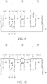
- FIG. 1 is a top view of a semiconductor structure according to an embodiment of the invention.
- FIG. 2 is a schematic cross-sectional view taken along the line I-I′ in FIG. 1 .
- FIG. 3 to FIG. 15 illustrate a method of forming a semiconductor structure.
- FIG. 1 is a top view of a semiconductor structure according to an embodiment of the present invention.
- FIG. 2 is a schematic cross-sectional view taken along the line I-I′ in FIG. 1 .
- the semiconductor structure 1 includes a substrate 100 , for example, a silicon substrate, having a first region R 1 and a second region R 2 around the first region R 1 .
- the second region R 2 may surround the first region R 1 .
- the semiconductor structure 1 may be, for example, a part of a static random access memory, wherein the first region R 1 may be the area as indicated by the dotted line.
- the first region R 1 includes at least two PMOS pull-up transistors PL 1 and PL 2 .
- the first region R 1 may be a PMOS region, that is, only PMOS transistors are provided in the first region R 1
- the second region R 2 may be an NMOS region, that is, only NMOS transistors are provided in the second region R 2 .
- FIG. 1 four active regions AA 1 to AA 4 extending along the reference Y axis and four gates G 1 to G 4 extending along the reference X axis are illustrated.
- the gate G 1 crosses the active area AA 2 to form a PMOS pull-up transistor PL 1
- the gate G 2 crosses the active area AA 3 to form a PMOS pull-up transistor PL 2 .
- STI shallow trench isolation
- the semiconductor structure 1 includes at least one first fin structure F 1 disposed in the first region R 1 , and at least one second fin structure F 2 disposed in the second region R 2 .
- a first isolation trench T 1 is provided adjacent to the first fin structure F 1 .
- a first trench isolation layer IM 1 such as a silicon oxide layer, is provided in the first isolation trench T 1 .
- a second isolation trench T 2 is provided around the first region R 1 .
- the second isolation trench T 2 is located between the first fin structure F 1 and the second fin structure F 2 .
- a second trench isolation layer IM 2 such as a silicon oxide layer, is provided in the second isolation trench T 2 .
- the bottom surface S of the second isolation trench T 2 has a step height H.
- the bottom surface S of the second isolation trench T 2 includes a first surface S 1 in the first region R 1 and a second surface S 2 in the second region R 2 , and the first surface S 1 is lower than the second surface S 2 , thereby constituting the step height H at the interface between the first region R 1 and the second region R 2 .
- the step height H is about 30-100 angstroms, but it is not limited thereto.
- the top surface ST 1 of the first trench isolation layer IM 1 and the top surface ST 2 of the second trench isolation layer IM 2 are coplanar. According to an embodiment of the present invention, the top surface FST 1 of the first fin structure F 1 is lower than the top surface FST 2 of the second fin structure F 2 .
- the gate G 1 of the semiconductor structure 1 may be disposed on the first fin structure F 1 .
- a first source region SD 1 adjacent to the gate G 1 for example, a P + doped region, is provided on the first fin structure F 1 .
- a first drain region DD 1 adjacent to the gate G 1 for example, a P + doped region, is provided on the first fin structure F 1 .
- the gate G 1 , the first source region SD 1 and the first drain region DD 1 may constitute the PMOS pull-up transistor PL 1 .
- the first source region SD 1 and the first drain region DD 1 include an epitaxial SiGe layer SG 1 , which has a height h of about 5-25 nm above the top surface ST 1 of the first trench isolation layer EVIL but not limited to this.
- the distance W between the epitaxial SiGe layer SG 1 and the adjacent epitaxial SiGe layer SG 2 on the top surface ST 1 of the first trench isolation layer IM 1 is at least 20 nm, for example, between 20 and 60 nm. Therefore, the semiconductor structure 1 of the present invention can effectively avoid the short circuit problem caused by the SiGe bridge.
- the gate G 2 of the semiconductor structure 1 may be disposed on the second fin structure F 2 .
- a second source region SD 2 adjacent to the gate G 2 is provided on the second fin structure F 2 .
- a second drain region DD 2 adjacent to the gate G 2 is provided on the second fin structure F 2 .
- the gate G 2 , the second source region SD 2 and the second drain region DD 2 can constitute an NMOS transistor.
- the second source region SD 2 and the second drain region DD 2 include an epitaxial SiP layer SPE.
- FIG. 3 to FIG. 15 illustrate a method of forming a semiconductor structure.
- a substrate 100 such as a silicon substrate, is provided with a first region R 1 and a second region R 2 around the first region R 1 .
- the second region R 2 may surround the first region R 1 .
- the first region R 1 may be a PMOS region, that is, only PMOS transistors are provided in the first region R 1
- the second region R 2 may be an NMOS region, that is, only NMOS transistors are provide in the second region R 2 .
- the substrate 100 in the first region R 1 is etched to form a recess RA in the first region R 1 , and a step height RH is formed at the interface between the first region R 1 and the second region R 2 .
- the step height RH is about 30-100 angstroms, but it is not limited thereto.
- a hard mask layer HM is then deposited on the substrate 100 in a blanket manner.
- the hard mask layer HM may include a silicon nitride layer, but is not limited thereto.
- a trench isolation process is performed.
- a lithographic process and an etching process may be performed to etch the hard mask layer HM and the substrate 100 in the predetermined area, and a first isolation trench T 1 is formed in the first area R 1 , and a second isolation trench T 2 is formed around the first area R 1 .
- at least one first fin structure F 1 is formed in the first region R 1
- at least one second fin structure F 2 is formed in the second region R 2 .
- the second isolation trench T 2 is located between the first fin structure F 1 and the second fin structure F 2 .
- Between two fin-like structures F 2 for example, the top surface FST 1 of the first fin structure F 1 is lower than the top surface FST 2 of the second fin structure F 2 by about 30-100 angstroms.
- the bottom surface S of the second isolation trench T 2 has a step height H.
- the bottom surface S of the second isolation trench T 2 includes a first surface S 1 in the first region R 1 and a second surface S 2 in the second region R 2 , and the first surface S 1 is lower than the first surface S 1 , thereby forming a step height H at the interface between the first region R 1 and the second region R 2 .
- the step height H is about 30-100 angstroms, but it is not limited thereto.
- a chemical vapor deposition (CVD) process is then performed to deposit an insulating layer 102 , such as a silicon oxide layer, on the substrate 100 in a blanket manner.
- the insulating layer 102 covers the hard mask layer HM, and fills the first isolation trench T 1 and the second isolation trench T 2 .
- the insulating layer 102 is then subjected to a planarization process, for example, a chemical mechanical polishing (CMP) process, to polish the insulating layer 102 until the top surface of the hard mask layer HM in the second region R 2 is first exposed. At this point, the top surface of the hard mask layer HM in the first region R 1 may still be covered by the insulating layer 102 .
- CMP chemical mechanical polishing
- an etch-back process is then performed, using dry etching or wet etching to etch away the insulating layer 102 of a predetermined thickness, revealing the top surface of the hard mask layer HM in the first region R 1 , so that a first trench isolation layer IM 1 is formed in the first isolation trench T 1 , and a second trench isolation layer IM 2 is formed in the second isolation trench T 2 .
- the top surface ST 1 of the first trench isolation layer IM 1 and the top surface ST 2 of the second trench isolation layer IM 2 are coplanar.
- an etching process such as wet etching, is then used to remove the hard mask layer HM to reveal the top surface FST 1 of the first fin structure F 1 and the top surface FST 2 of the second fin structure F 2 .
- the top surface ST 1 of the first trench isolation layer IM 1 and the top surface ST 2 of the second trench isolation layer IM 2 are higher than the top surface FST 2 of the second fin structure F 2
- the top surface FST 2 of the second fin structure F 2 is higher than the top surface FST 1 of the first fin structure F 1
- the height difference ht between the top surface FST 2 of the second fin structure F 2 and the top surface FST 1 of the first fin structure F 1 is about 30-100 angstroms, but is not limited thereto.
- an ion implantation process is then performed to form ion wells, such as P-type wells or N-type wells (not shown) in the substrate 100 .
- a cleaning process is performed. The above cleaning process may consume part of the thickness of the first trench isolation layer IM 1 and the second trench isolation layer IM 2 , so that the top surface ST 1 of the first trench isolation layer IM 1 and the top surface ST 2 of the second trench isolation layer IM 2 will be closer to the top surface FST 2 of the second fin structure F 2 , but still higher than the top surface FST 1 of the first fin structure F 1 .
- the height difference ht between the top surface ST 1 of the first trench isolation layer IM 1 and the top surface FST 1 of the first fin structure F 1 is about 30-100 angstroms, but is not limited thereto.
- the upper corners of the first trench isolation layer IM 1 will be rounded.
- an oxidation process is then performed to form a gate oxide layer GOX 1 and a gate oxide layer GOX 2 on the top surface FST 1 of the first fin structure F 1 and the top surface FST 2 of the second fin structure F 2 , respectively.
- the gate oxide layer GOX 1 and the gate oxide layer GOX 2 may include silicon oxide layers, but are not limited thereto.
- the gate oxide layer GOX 1 and the gate oxide layer GOX 2 may be formed of the same material.
- the gate oxide layer GOX 1 and the gate oxide layer GOX 2 may be formed of different materials.
- a polysilicon layer POL is then deposited on the substrate 100 in a blanket manner.
- the polysilicon layer POL is patterned by using a lithographic process and an etching processes to form a gate G 1 on the first fin structure F 1 and a gate G 2 on the second fin structure F 2 (as shown in FIG. 1 ). Since the polysilicon layer POL on this cross-section is removed, only the outline of the gate G 2 is shown by dotted lines in the figure. Subsequently, spacers (not shown) can be formed on the gate G 1 and the gate G 2 .
- a recessed region RE 1 and a recessed region RE 2 adjacent to the gate G 1 are then formed on the first fin structures F 1 in the first region R 1 .
- the method of forming the recessed region RE 1 and the recessed region RE 2 on the first fin structures F 1 may comprise wet etching, but is not limited thereto.
- the recessed region RE 1 and the recessed region RE 2 are separated by the first trench isolation layer IM 1 .
- the top surface ST 1 of the first trench isolation layer IM 1 and the top surface ST 2 of the second trench isolation layer IM 2 are still coplanar.
- an epitaxial process is then performed to form an epitaxial SiGe layer SG 1 and an epitaxial SiGe layer SG 2 in the recessed region RE 1 and the recessed region RE 2 in the first region R 1 , respectively.
- the epitaxial SiGe layer SG 1 and the epitaxial SiGe layer SG 2 can be formed by an organometallic vapor phase epitaxy method, but are not limited thereto.
- the second region R 2 can be masked.
- the distance W between the epitaxial SiGe layer SG 1 and the adjacent epitaxial SiGe layer SG 2 on the top surface ST 1 of the first trench isolation layer IM 1 is at least 20 nm, for example, between 20 and 60 nm. Therefore, the semiconductor structure 1 of the present invention can effectively avoid the short circuit problem caused by the SiGe bridge.
- the epitaxy process is performed to form an epitaxial SiP layer SPE on the second fin structure F 2 in the second region R 2 .
Landscapes
- Insulated Gate Type Field-Effect Transistor (AREA)
Abstract
Description
Claims (18)
Applications Claiming Priority (2)
| Application Number | Priority Date | Filing Date | Title |
|---|---|---|---|
| CN202110047083.XA CN114765171B (en) | 2021-01-14 | 2021-01-14 | Semiconductor structure and manufacturing method thereof |
| CN202110047083.X | 2021-01-14 |
Publications (2)
| Publication Number | Publication Date |
|---|---|
| US20220223720A1 US20220223720A1 (en) | 2022-07-14 |
| US11515404B2 true US11515404B2 (en) | 2022-11-29 |
Family
ID=82323328
Family Applications (1)
| Application Number | Title | Priority Date | Filing Date |
|---|---|---|---|
| US17/160,427 Active 2041-03-06 US11515404B2 (en) | 2021-01-14 | 2021-01-28 | Semiconductor structure comprising regions having an isolation trench with a stepped bottom surface therebetween and method of forming the same |
Country Status (2)
| Country | Link |
|---|---|
| US (1) | US11515404B2 (en) |
| CN (1) | CN114765171B (en) |
Families Citing this family (1)
| Publication number | Priority date | Publication date | Assignee | Title |
|---|---|---|---|---|
| US12040219B2 (en) | 2021-03-19 | 2024-07-16 | Taiwan Semiconductor Manufacturing Company, Ltd. | Etch profile control of isolation trench |
Citations (12)
| Publication number | Priority date | Publication date | Assignee | Title |
|---|---|---|---|---|
| KR101153158B1 (en) | 2010-03-01 | 2012-07-03 | 타이완 세미콘덕터 매뉴팩쳐링 컴퍼니 리미티드 | Dual epitaxial process for a finfet device |
| US20160211168A1 (en) * | 2015-01-21 | 2016-07-21 | Sunhom Steve Paak | Semiconductor Devices Including Active Patterns Having Different Pitches and Methods of Fabricating the Same |
| US9443962B2 (en) | 2012-11-09 | 2016-09-13 | Taiwan Semiconductor Manufacturing Company, Ltd. | Recessing STI to increase fin height in fin-first process |
| US9595611B2 (en) | 2013-08-01 | 2017-03-14 | Samsung Electronics Co., Ltd. | FinFET with a single contact to multiple fins bridged together to form a source/drain region of the transistor |
| US9735158B2 (en) | 2014-05-13 | 2017-08-15 | Samsung Electronics Co., Ltd. | Semiconductor devices having bridge layer and methods of manufacturing the same |
| US9793174B1 (en) | 2016-08-05 | 2017-10-17 | United Microelectronics Corp. | FinFET device on silicon-on-insulator and method of forming the same |
| US20180342607A1 (en) * | 2017-05-24 | 2018-11-29 | Semiconductor Manufacturing International (Shanghai) Corporation | Semiconductor structure and fabrication method thereof |
| US20190097056A1 (en) * | 2017-09-28 | 2019-03-28 | Taiwan Semiconductor Manufacturing Co., Ltd. | Semiconductor device having fins and method of fabricating the same |
| US10541253B2 (en) | 2017-01-10 | 2020-01-21 | International Business Machines Corporation | FinFETs with various fin height |
| US20200194440A1 (en) * | 2018-12-14 | 2020-06-18 | Qualcomm Incorporated | Sram source-drain structure |
| US20210265224A1 (en) * | 2020-02-26 | 2021-08-26 | Taiwan Semiconductor Manufacturing Co., Ltd. | Semiconductor Device with Dual Isolation Liner and Method of Forming the Same |
| US20210313181A1 (en) * | 2020-04-01 | 2021-10-07 | Taiwan Semiconductor Manufacturing Company, Ltd. | Cut metal gate refill with void |
Family Cites Families (8)
| Publication number | Priority date | Publication date | Assignee | Title |
|---|---|---|---|---|
| KR20150015187A (en) * | 2013-07-31 | 2015-02-10 | 삼성전자주식회사 | Semiconductor device and method for fabricating the same |
| KR102231208B1 (en) * | 2014-07-21 | 2021-03-24 | 삼성전자주식회사 | Method of manufacturing semiconductor device |
| CN106711213B (en) * | 2015-07-20 | 2021-02-26 | 联华电子股份有限公司 | Semiconductor element and manufacturing method thereof |
| US10529712B2 (en) * | 2017-11-07 | 2020-01-07 | Samsung Electronics Co., Ltd. | Semiconductor device |
| KR102532118B1 (en) * | 2018-03-20 | 2023-05-11 | 삼성전자주식회사 | Semiconductor device and method for fabricating the same |
| US10665697B2 (en) * | 2018-06-15 | 2020-05-26 | Taiwan Semiconductor Manufacturing Company, Ltd. | Semiconductor device and method |
| KR102453022B1 (en) * | 2018-09-04 | 2022-10-07 | 삼성전자주식회사 | Semiconductor device and method for fabricating the same |
| CN111341847B (en) * | 2018-12-19 | 2023-03-28 | 联华电子股份有限公司 | Semiconductor structure and manufacturing method thereof |
-
2021
- 2021-01-14 CN CN202110047083.XA patent/CN114765171B/en active Active
- 2021-01-28 US US17/160,427 patent/US11515404B2/en active Active
Patent Citations (12)
| Publication number | Priority date | Publication date | Assignee | Title |
|---|---|---|---|---|
| KR101153158B1 (en) | 2010-03-01 | 2012-07-03 | 타이완 세미콘덕터 매뉴팩쳐링 컴퍼니 리미티드 | Dual epitaxial process for a finfet device |
| US9443962B2 (en) | 2012-11-09 | 2016-09-13 | Taiwan Semiconductor Manufacturing Company, Ltd. | Recessing STI to increase fin height in fin-first process |
| US9595611B2 (en) | 2013-08-01 | 2017-03-14 | Samsung Electronics Co., Ltd. | FinFET with a single contact to multiple fins bridged together to form a source/drain region of the transistor |
| US9735158B2 (en) | 2014-05-13 | 2017-08-15 | Samsung Electronics Co., Ltd. | Semiconductor devices having bridge layer and methods of manufacturing the same |
| US20160211168A1 (en) * | 2015-01-21 | 2016-07-21 | Sunhom Steve Paak | Semiconductor Devices Including Active Patterns Having Different Pitches and Methods of Fabricating the Same |
| US9793174B1 (en) | 2016-08-05 | 2017-10-17 | United Microelectronics Corp. | FinFET device on silicon-on-insulator and method of forming the same |
| US10541253B2 (en) | 2017-01-10 | 2020-01-21 | International Business Machines Corporation | FinFETs with various fin height |
| US20180342607A1 (en) * | 2017-05-24 | 2018-11-29 | Semiconductor Manufacturing International (Shanghai) Corporation | Semiconductor structure and fabrication method thereof |
| US20190097056A1 (en) * | 2017-09-28 | 2019-03-28 | Taiwan Semiconductor Manufacturing Co., Ltd. | Semiconductor device having fins and method of fabricating the same |
| US20200194440A1 (en) * | 2018-12-14 | 2020-06-18 | Qualcomm Incorporated | Sram source-drain structure |
| US20210265224A1 (en) * | 2020-02-26 | 2021-08-26 | Taiwan Semiconductor Manufacturing Co., Ltd. | Semiconductor Device with Dual Isolation Liner and Method of Forming the Same |
| US20210313181A1 (en) * | 2020-04-01 | 2021-10-07 | Taiwan Semiconductor Manufacturing Company, Ltd. | Cut metal gate refill with void |
Also Published As
| Publication number | Publication date |
|---|---|
| CN114765171A (en) | 2022-07-19 |
| US20220223720A1 (en) | 2022-07-14 |
| CN114765171B (en) | 2025-09-05 |
Similar Documents
| Publication | Publication Date | Title |
|---|---|---|
| US7176084B2 (en) | Self-aligned conductive spacer process for sidewall control gate of high-speed random access memory | |
| US10079290B2 (en) | Semiconductor device having asymmetric spacer structures | |
| US8790991B2 (en) | Method and structure for shallow trench isolation to mitigate active shorts | |
| US8962430B2 (en) | Method for the formation of a protective dual liner for a shallow trench isolation structure | |
| US11792981B2 (en) | Two dimensional structure to control flash operation and methods for forming the same | |
| TW202523071A (en) | Memory structure | |
| KR100642754B1 (en) | Semiconductor device having etch resistant L shape spacer and fabrication method thereof | |
| US10573753B1 (en) | Oxide spacer in a contact over active gate finFET and method of production thereof | |
| US10347541B1 (en) | Active gate contacts and method of fabrication thereof | |
| US20190013204A1 (en) | Method of fabricating buried word line and gate on finfet | |
| US11515404B2 (en) | Semiconductor structure comprising regions having an isolation trench with a stepped bottom surface therebetween and method of forming the same | |
| CN114121663B (en) | Method for forming semiconductor device | |
| US10580684B2 (en) | Self-aligned single diffusion break for fully depleted silicon-on-insulator and method for producing the same | |
| CN112687622B (en) | Single diffusion region cutting structure of fin field effect transistor and forming method thereof | |
| US20130146966A1 (en) | Semiconductor structure with enhanced cap and fabrication method thereof | |
| US20070170511A1 (en) | Method for fabricating a recessed-gate mos transistor device | |
| US10707225B2 (en) | Semiconductor memory device and fabrication method thereof | |
| US10186524B2 (en) | Fully depleted silicon-on-insulator (FDSOI) transistor device and self-aligned active area in FDSOI bulk exposed regions | |
| KR100481987B1 (en) | (Method for fabricating MOS capacitor of semiconductor device | |
| CN113809008A (en) | Semiconductor structure and method of forming the same | |
| US20260047127A1 (en) | Semiconductor device and method for fabricating the same | |
| US11699730B2 (en) | Semiconductor memory device and fabrication method thereof | |
| CN110707086B (en) | Semiconductor device with a plurality of semiconductor chips | |
| US10141194B1 (en) | Manufacturing method of semiconductor structure | |
| KR100266028B1 (en) | Semiconductor device and method for fabricating the same |
Legal Events
| Date | Code | Title | Description |
|---|---|---|---|
| AS | Assignment |
Owner name: UNITED MICROELECTRONICS CORP., TAIWAN Free format text: ASSIGNMENT OF ASSIGNORS INTEREST;ASSIGNORS:YANG, TSUNG-YU;LI, SHIN-HUNG;TSAO, RUEI-JHE;AND OTHERS;REEL/FRAME:055070/0673 Effective date: 20201230 |
|
| FEPP | Fee payment procedure |
Free format text: ENTITY STATUS SET TO UNDISCOUNTED (ORIGINAL EVENT CODE: BIG.); ENTITY STATUS OF PATENT OWNER: LARGE ENTITY |
|
| STPP | Information on status: patent application and granting procedure in general |
Free format text: RESPONSE TO NON-FINAL OFFICE ACTION ENTERED AND FORWARDED TO EXAMINER |
|
| STPP | Information on status: patent application and granting procedure in general |
Free format text: NOTICE OF ALLOWANCE MAILED -- APPLICATION RECEIVED IN OFFICE OF PUBLICATIONS |
|
| STPP | Information on status: patent application and granting procedure in general |
Free format text: PUBLICATIONS -- ISSUE FEE PAYMENT VERIFIED |
|
| STCF | Information on status: patent grant |
Free format text: PATENTED CASE |
|
| MAFP | Maintenance fee payment |
Free format text: PAYMENT OF MAINTENANCE FEE, 4TH YEAR, LARGE ENTITY (ORIGINAL EVENT CODE: M1551); ENTITY STATUS OF PATENT OWNER: LARGE ENTITY Year of fee payment: 4 |