US11515404B2 - Semiconductor structure comprising regions having an isolation trench with a stepped bottom surface therebetween and method of forming the same - Google Patents
Semiconductor structure comprising regions having an isolation trench with a stepped bottom surface therebetween and method of forming the same Download PDFInfo
- Publication number
- US11515404B2 US11515404B2 US17/160,427 US202117160427A US11515404B2 US 11515404 B2 US11515404 B2 US 11515404B2 US 202117160427 A US202117160427 A US 202117160427A US 11515404 B2 US11515404 B2 US 11515404B2
- Authority
- US
- United States
- Prior art keywords
- region
- fin structure
- trench
- gate
- layer
- Prior art date
- Legal status (The legal status is an assumption and is not a legal conclusion. Google has not performed a legal analysis and makes no representation as to the accuracy of the status listed.)
- Active, expires
Links
- 238000002955 isolation Methods 0.000 title claims abstract description 88
- 239000004065 semiconductor Substances 0.000 title claims abstract description 31
- 238000000034 method Methods 0.000 title claims description 42
- 239000000758 substrate Substances 0.000 claims abstract description 17
- 229910000577 Silicon-germanium Inorganic materials 0.000 claims description 17
- 238000005530 etching Methods 0.000 claims description 5
- 101100281682 Danio rerio fsta gene Proteins 0.000 description 8
- 102100038837 2-Hydroxyacid oxidase 1 Human genes 0.000 description 4
- 101001015570 Arabidopsis thaliana Glycolate oxidase 1 Proteins 0.000 description 4
- 101000887873 Arabidopsis thaliana Glycolate oxidase 2 Proteins 0.000 description 4
- 101001031589 Homo sapiens 2-Hydroxyacid oxidase 1 Proteins 0.000 description 4
- VYPSYNLAJGMNEJ-UHFFFAOYSA-N Silicium dioxide Chemical compound O=[Si]=O VYPSYNLAJGMNEJ-UHFFFAOYSA-N 0.000 description 4
- 229910052814 silicon oxide Inorganic materials 0.000 description 4
- 238000004140 cleaning Methods 0.000 description 3
- 238000004519 manufacturing process Methods 0.000 description 3
- 229910021420 polycrystalline silicon Inorganic materials 0.000 description 3
- 229920005591 polysilicon Polymers 0.000 description 3
- 238000001039 wet etching Methods 0.000 description 3
- XUIMIQQOPSSXEZ-UHFFFAOYSA-N Silicon Chemical compound [Si] XUIMIQQOPSSXEZ-UHFFFAOYSA-N 0.000 description 2
- 238000005229 chemical vapour deposition Methods 0.000 description 2
- 239000000463 material Substances 0.000 description 2
- 229910052710 silicon Inorganic materials 0.000 description 2
- 239000010703 silicon Substances 0.000 description 2
- 230000003068 static effect Effects 0.000 description 2
- 229910052581 Si3N4 Inorganic materials 0.000 description 1
- 230000004075 alteration Effects 0.000 description 1
- 230000007812 deficiency Effects 0.000 description 1
- 238000001312 dry etching Methods 0.000 description 1
- 238000005516 engineering process Methods 0.000 description 1
- 238000000407 epitaxy Methods 0.000 description 1
- 238000005468 ion implantation Methods 0.000 description 1
- 150000002500 ions Chemical class 0.000 description 1
- 238000012986 modification Methods 0.000 description 1
- 230000004048 modification Effects 0.000 description 1
- 125000002524 organometallic group Chemical group 0.000 description 1
- 230000003647 oxidation Effects 0.000 description 1
- 238000007254 oxidation reaction Methods 0.000 description 1
- 238000005498 polishing Methods 0.000 description 1
- HQVNEWCFYHHQES-UHFFFAOYSA-N silicon nitride Chemical compound N12[Si]34N5[Si]62N3[Si]51N64 HQVNEWCFYHHQES-UHFFFAOYSA-N 0.000 description 1
- 125000006850 spacer group Chemical group 0.000 description 1
- 239000000126 substance Substances 0.000 description 1
- 238000000927 vapour-phase epitaxy Methods 0.000 description 1
Images


Classifications
-
- H—ELECTRICITY
- H01—ELECTRIC ELEMENTS
- H01L—SEMICONDUCTOR DEVICES NOT COVERED BY CLASS H10
- H01L29/00—Semiconductor devices adapted for rectifying, amplifying, oscillating or switching, or capacitors or resistors with at least one potential-jump barrier or surface barrier, e.g. PN junction depletion layer or carrier concentration layer; Details of semiconductor bodies or of electrodes thereof ; Multistep manufacturing processes therefor
- H01L29/66—Types of semiconductor device ; Multistep manufacturing processes therefor
- H01L29/66007—Multistep manufacturing processes
- H01L29/66075—Multistep manufacturing processes of devices having semiconductor bodies comprising group 14 or group 13/15 materials
- H01L29/66227—Multistep manufacturing processes of devices having semiconductor bodies comprising group 14 or group 13/15 materials the devices being controllable only by the electric current supplied or the electric potential applied, to an electrode which does not carry the current to be rectified, amplified or switched, e.g. three-terminal devices
- H01L29/66409—Unipolar field-effect transistors
- H01L29/66477—Unipolar field-effect transistors with an insulated gate, i.e. MISFET
- H01L29/66787—Unipolar field-effect transistors with an insulated gate, i.e. MISFET with a gate at the side of the channel
- H01L29/66795—Unipolar field-effect transistors with an insulated gate, i.e. MISFET with a gate at the side of the channel with a horizontal current flow in a vertical sidewall of a semiconductor body, e.g. FinFET, MuGFET
-
- H—ELECTRICITY
- H01—ELECTRIC ELEMENTS
- H01L—SEMICONDUCTOR DEVICES NOT COVERED BY CLASS H10
- H01L27/00—Devices consisting of a plurality of semiconductor or other solid-state components formed in or on a common substrate
- H01L27/02—Devices consisting of a plurality of semiconductor or other solid-state components formed in or on a common substrate including semiconductor components specially adapted for rectifying, oscillating, amplifying or switching and having at least one potential-jump barrier or surface barrier; including integrated passive circuit elements with at least one potential-jump barrier or surface barrier
- H01L27/04—Devices consisting of a plurality of semiconductor or other solid-state components formed in or on a common substrate including semiconductor components specially adapted for rectifying, oscillating, amplifying or switching and having at least one potential-jump barrier or surface barrier; including integrated passive circuit elements with at least one potential-jump barrier or surface barrier the substrate being a semiconductor body
- H01L27/08—Devices consisting of a plurality of semiconductor or other solid-state components formed in or on a common substrate including semiconductor components specially adapted for rectifying, oscillating, amplifying or switching and having at least one potential-jump barrier or surface barrier; including integrated passive circuit elements with at least one potential-jump barrier or surface barrier the substrate being a semiconductor body including only semiconductor components of a single kind
- H01L27/085—Devices consisting of a plurality of semiconductor or other solid-state components formed in or on a common substrate including semiconductor components specially adapted for rectifying, oscillating, amplifying or switching and having at least one potential-jump barrier or surface barrier; including integrated passive circuit elements with at least one potential-jump barrier or surface barrier the substrate being a semiconductor body including only semiconductor components of a single kind including field-effect components only
- H01L27/088—Devices consisting of a plurality of semiconductor or other solid-state components formed in or on a common substrate including semiconductor components specially adapted for rectifying, oscillating, amplifying or switching and having at least one potential-jump barrier or surface barrier; including integrated passive circuit elements with at least one potential-jump barrier or surface barrier the substrate being a semiconductor body including only semiconductor components of a single kind including field-effect components only the components being field-effect transistors with insulated gate
- H01L27/0886—Devices consisting of a plurality of semiconductor or other solid-state components formed in or on a common substrate including semiconductor components specially adapted for rectifying, oscillating, amplifying or switching and having at least one potential-jump barrier or surface barrier; including integrated passive circuit elements with at least one potential-jump barrier or surface barrier the substrate being a semiconductor body including only semiconductor components of a single kind including field-effect components only the components being field-effect transistors with insulated gate including transistors with a horizontal current flow in a vertical sidewall of a semiconductor body, e.g. FinFET, MuGFET
-
- H—ELECTRICITY
- H01—ELECTRIC ELEMENTS
- H01L—SEMICONDUCTOR DEVICES NOT COVERED BY CLASS H10
- H01L21/00—Processes or apparatus adapted for the manufacture or treatment of semiconductor or solid state devices or of parts thereof
- H01L21/70—Manufacture or treatment of devices consisting of a plurality of solid state components formed in or on a common substrate or of parts thereof; Manufacture of integrated circuit devices or of parts thereof
- H01L21/71—Manufacture of specific parts of devices defined in group H01L21/70
- H01L21/76—Making of isolation regions between components
- H01L21/762—Dielectric regions, e.g. EPIC dielectric isolation, LOCOS; Trench refilling techniques, SOI technology, use of channel stoppers
- H01L21/76224—Dielectric regions, e.g. EPIC dielectric isolation, LOCOS; Trench refilling techniques, SOI technology, use of channel stoppers using trench refilling with dielectric materials
- H01L21/76229—Concurrent filling of a plurality of trenches having a different trench shape or dimension, e.g. rectangular and V-shaped trenches, wide and narrow trenches, shallow and deep trenches
-
- H—ELECTRICITY
- H01—ELECTRIC ELEMENTS
- H01L—SEMICONDUCTOR DEVICES NOT COVERED BY CLASS H10
- H01L21/00—Processes or apparatus adapted for the manufacture or treatment of semiconductor or solid state devices or of parts thereof
- H01L21/70—Manufacture or treatment of devices consisting of a plurality of solid state components formed in or on a common substrate or of parts thereof; Manufacture of integrated circuit devices or of parts thereof
- H01L21/71—Manufacture of specific parts of devices defined in group H01L21/70
- H01L21/76—Making of isolation regions between components
- H01L21/762—Dielectric regions, e.g. EPIC dielectric isolation, LOCOS; Trench refilling techniques, SOI technology, use of channel stoppers
- H01L21/76224—Dielectric regions, e.g. EPIC dielectric isolation, LOCOS; Trench refilling techniques, SOI technology, use of channel stoppers using trench refilling with dielectric materials
- H01L21/76232—Dielectric regions, e.g. EPIC dielectric isolation, LOCOS; Trench refilling techniques, SOI technology, use of channel stoppers using trench refilling with dielectric materials of trenches having a shape other than rectangular or V-shape, e.g. rounded corners, oblique or rounded trench walls
-
- H—ELECTRICITY
- H01—ELECTRIC ELEMENTS
- H01L—SEMICONDUCTOR DEVICES NOT COVERED BY CLASS H10
- H01L21/00—Processes or apparatus adapted for the manufacture or treatment of semiconductor or solid state devices or of parts thereof
- H01L21/70—Manufacture or treatment of devices consisting of a plurality of solid state components formed in or on a common substrate or of parts thereof; Manufacture of integrated circuit devices or of parts thereof
- H01L21/77—Manufacture or treatment of devices consisting of a plurality of solid state components or integrated circuits formed in, or on, a common substrate
- H01L21/78—Manufacture or treatment of devices consisting of a plurality of solid state components or integrated circuits formed in, or on, a common substrate with subsequent division of the substrate into plural individual devices
- H01L21/82—Manufacture or treatment of devices consisting of a plurality of solid state components or integrated circuits formed in, or on, a common substrate with subsequent division of the substrate into plural individual devices to produce devices, e.g. integrated circuits, each consisting of a plurality of components
- H01L21/822—Manufacture or treatment of devices consisting of a plurality of solid state components or integrated circuits formed in, or on, a common substrate with subsequent division of the substrate into plural individual devices to produce devices, e.g. integrated circuits, each consisting of a plurality of components the substrate being a semiconductor, using silicon technology
- H01L21/8232—Field-effect technology
- H01L21/8234—MIS technology, i.e. integration processes of field effect transistors of the conductor-insulator-semiconductor type
- H01L21/823431—MIS technology, i.e. integration processes of field effect transistors of the conductor-insulator-semiconductor type with a particular manufacturing method of transistors with a horizontal current flow in a vertical sidewall of a semiconductor body, e.g. FinFET, MuGFET
-
- H—ELECTRICITY
- H01—ELECTRIC ELEMENTS
- H01L—SEMICONDUCTOR DEVICES NOT COVERED BY CLASS H10
- H01L21/00—Processes or apparatus adapted for the manufacture or treatment of semiconductor or solid state devices or of parts thereof
- H01L21/70—Manufacture or treatment of devices consisting of a plurality of solid state components formed in or on a common substrate or of parts thereof; Manufacture of integrated circuit devices or of parts thereof
- H01L21/77—Manufacture or treatment of devices consisting of a plurality of solid state components or integrated circuits formed in, or on, a common substrate
- H01L21/78—Manufacture or treatment of devices consisting of a plurality of solid state components or integrated circuits formed in, or on, a common substrate with subsequent division of the substrate into plural individual devices
- H01L21/82—Manufacture or treatment of devices consisting of a plurality of solid state components or integrated circuits formed in, or on, a common substrate with subsequent division of the substrate into plural individual devices to produce devices, e.g. integrated circuits, each consisting of a plurality of components
- H01L21/822—Manufacture or treatment of devices consisting of a plurality of solid state components or integrated circuits formed in, or on, a common substrate with subsequent division of the substrate into plural individual devices to produce devices, e.g. integrated circuits, each consisting of a plurality of components the substrate being a semiconductor, using silicon technology
- H01L21/8232—Field-effect technology
- H01L21/8234—MIS technology, i.e. integration processes of field effect transistors of the conductor-insulator-semiconductor type
- H01L21/8238—Complementary field-effect transistors, e.g. CMOS
- H01L21/823807—Complementary field-effect transistors, e.g. CMOS with a particular manufacturing method of the channel structures, e.g. channel implants, halo or pocket implants, or channel materials
-
- H—ELECTRICITY
- H01—ELECTRIC ELEMENTS
- H01L—SEMICONDUCTOR DEVICES NOT COVERED BY CLASS H10
- H01L21/00—Processes or apparatus adapted for the manufacture or treatment of semiconductor or solid state devices or of parts thereof
- H01L21/70—Manufacture or treatment of devices consisting of a plurality of solid state components formed in or on a common substrate or of parts thereof; Manufacture of integrated circuit devices or of parts thereof
- H01L21/77—Manufacture or treatment of devices consisting of a plurality of solid state components or integrated circuits formed in, or on, a common substrate
- H01L21/78—Manufacture or treatment of devices consisting of a plurality of solid state components or integrated circuits formed in, or on, a common substrate with subsequent division of the substrate into plural individual devices
- H01L21/82—Manufacture or treatment of devices consisting of a plurality of solid state components or integrated circuits formed in, or on, a common substrate with subsequent division of the substrate into plural individual devices to produce devices, e.g. integrated circuits, each consisting of a plurality of components
- H01L21/822—Manufacture or treatment of devices consisting of a plurality of solid state components or integrated circuits formed in, or on, a common substrate with subsequent division of the substrate into plural individual devices to produce devices, e.g. integrated circuits, each consisting of a plurality of components the substrate being a semiconductor, using silicon technology
- H01L21/8232—Field-effect technology
- H01L21/8234—MIS technology, i.e. integration processes of field effect transistors of the conductor-insulator-semiconductor type
- H01L21/8238—Complementary field-effect transistors, e.g. CMOS
- H01L21/823814—Complementary field-effect transistors, e.g. CMOS with a particular manufacturing method of the source or drain structures, e.g. specific source or drain implants or silicided source or drain structures or raised source or drain structures
-
- H—ELECTRICITY
- H01—ELECTRIC ELEMENTS
- H01L—SEMICONDUCTOR DEVICES NOT COVERED BY CLASS H10
- H01L21/00—Processes or apparatus adapted for the manufacture or treatment of semiconductor or solid state devices or of parts thereof
- H01L21/70—Manufacture or treatment of devices consisting of a plurality of solid state components formed in or on a common substrate or of parts thereof; Manufacture of integrated circuit devices or of parts thereof
- H01L21/77—Manufacture or treatment of devices consisting of a plurality of solid state components or integrated circuits formed in, or on, a common substrate
- H01L21/78—Manufacture or treatment of devices consisting of a plurality of solid state components or integrated circuits formed in, or on, a common substrate with subsequent division of the substrate into plural individual devices
- H01L21/82—Manufacture or treatment of devices consisting of a plurality of solid state components or integrated circuits formed in, or on, a common substrate with subsequent division of the substrate into plural individual devices to produce devices, e.g. integrated circuits, each consisting of a plurality of components
- H01L21/822—Manufacture or treatment of devices consisting of a plurality of solid state components or integrated circuits formed in, or on, a common substrate with subsequent division of the substrate into plural individual devices to produce devices, e.g. integrated circuits, each consisting of a plurality of components the substrate being a semiconductor, using silicon technology
- H01L21/8232—Field-effect technology
- H01L21/8234—MIS technology, i.e. integration processes of field effect transistors of the conductor-insulator-semiconductor type
- H01L21/8238—Complementary field-effect transistors, e.g. CMOS
- H01L21/823821—Complementary field-effect transistors, e.g. CMOS with a particular manufacturing method of transistors with a horizontal current flow in a vertical sidewall of a semiconductor body, e.g. FinFET, MuGFET
-
- H—ELECTRICITY
- H01—ELECTRIC ELEMENTS
- H01L—SEMICONDUCTOR DEVICES NOT COVERED BY CLASS H10
- H01L21/00—Processes or apparatus adapted for the manufacture or treatment of semiconductor or solid state devices or of parts thereof
- H01L21/70—Manufacture or treatment of devices consisting of a plurality of solid state components formed in or on a common substrate or of parts thereof; Manufacture of integrated circuit devices or of parts thereof
- H01L21/77—Manufacture or treatment of devices consisting of a plurality of solid state components or integrated circuits formed in, or on, a common substrate
- H01L21/78—Manufacture or treatment of devices consisting of a plurality of solid state components or integrated circuits formed in, or on, a common substrate with subsequent division of the substrate into plural individual devices
- H01L21/82—Manufacture or treatment of devices consisting of a plurality of solid state components or integrated circuits formed in, or on, a common substrate with subsequent division of the substrate into plural individual devices to produce devices, e.g. integrated circuits, each consisting of a plurality of components
- H01L21/822—Manufacture or treatment of devices consisting of a plurality of solid state components or integrated circuits formed in, or on, a common substrate with subsequent division of the substrate into plural individual devices to produce devices, e.g. integrated circuits, each consisting of a plurality of components the substrate being a semiconductor, using silicon technology
- H01L21/8232—Field-effect technology
- H01L21/8234—MIS technology, i.e. integration processes of field effect transistors of the conductor-insulator-semiconductor type
- H01L21/8238—Complementary field-effect transistors, e.g. CMOS
- H01L21/823878—Complementary field-effect transistors, e.g. CMOS isolation region manufacturing related aspects, e.g. to avoid interaction of isolation region with adjacent structure
-
- H—ELECTRICITY
- H01—ELECTRIC ELEMENTS
- H01L—SEMICONDUCTOR DEVICES NOT COVERED BY CLASS H10
- H01L27/00—Devices consisting of a plurality of semiconductor or other solid-state components formed in or on a common substrate
- H01L27/02—Devices consisting of a plurality of semiconductor or other solid-state components formed in or on a common substrate including semiconductor components specially adapted for rectifying, oscillating, amplifying or switching and having at least one potential-jump barrier or surface barrier; including integrated passive circuit elements with at least one potential-jump barrier or surface barrier
- H01L27/0203—Particular design considerations for integrated circuits
- H01L27/0207—Geometrical layout of the components, e.g. computer aided design; custom LSI, semi-custom LSI, standard cell technique
-
- H—ELECTRICITY
- H01—ELECTRIC ELEMENTS
- H01L—SEMICONDUCTOR DEVICES NOT COVERED BY CLASS H10
- H01L27/00—Devices consisting of a plurality of semiconductor or other solid-state components formed in or on a common substrate
- H01L27/02—Devices consisting of a plurality of semiconductor or other solid-state components formed in or on a common substrate including semiconductor components specially adapted for rectifying, oscillating, amplifying or switching and having at least one potential-jump barrier or surface barrier; including integrated passive circuit elements with at least one potential-jump barrier or surface barrier
- H01L27/04—Devices consisting of a plurality of semiconductor or other solid-state components formed in or on a common substrate including semiconductor components specially adapted for rectifying, oscillating, amplifying or switching and having at least one potential-jump barrier or surface barrier; including integrated passive circuit elements with at least one potential-jump barrier or surface barrier the substrate being a semiconductor body
- H01L27/08—Devices consisting of a plurality of semiconductor or other solid-state components formed in or on a common substrate including semiconductor components specially adapted for rectifying, oscillating, amplifying or switching and having at least one potential-jump barrier or surface barrier; including integrated passive circuit elements with at least one potential-jump barrier or surface barrier the substrate being a semiconductor body including only semiconductor components of a single kind
- H01L27/085—Devices consisting of a plurality of semiconductor or other solid-state components formed in or on a common substrate including semiconductor components specially adapted for rectifying, oscillating, amplifying or switching and having at least one potential-jump barrier or surface barrier; including integrated passive circuit elements with at least one potential-jump barrier or surface barrier the substrate being a semiconductor body including only semiconductor components of a single kind including field-effect components only
- H01L27/088—Devices consisting of a plurality of semiconductor or other solid-state components formed in or on a common substrate including semiconductor components specially adapted for rectifying, oscillating, amplifying or switching and having at least one potential-jump barrier or surface barrier; including integrated passive circuit elements with at least one potential-jump barrier or surface barrier the substrate being a semiconductor body including only semiconductor components of a single kind including field-effect components only the components being field-effect transistors with insulated gate
- H01L27/092—Devices consisting of a plurality of semiconductor or other solid-state components formed in or on a common substrate including semiconductor components specially adapted for rectifying, oscillating, amplifying or switching and having at least one potential-jump barrier or surface barrier; including integrated passive circuit elements with at least one potential-jump barrier or surface barrier the substrate being a semiconductor body including only semiconductor components of a single kind including field-effect components only the components being field-effect transistors with insulated gate complementary MIS field-effect transistors
- H01L27/0924—Devices consisting of a plurality of semiconductor or other solid-state components formed in or on a common substrate including semiconductor components specially adapted for rectifying, oscillating, amplifying or switching and having at least one potential-jump barrier or surface barrier; including integrated passive circuit elements with at least one potential-jump barrier or surface barrier the substrate being a semiconductor body including only semiconductor components of a single kind including field-effect components only the components being field-effect transistors with insulated gate complementary MIS field-effect transistors including transistors with a horizontal current flow in a vertical sidewall of a semiconductor body, e.g. FinFET, MuGFET
-
- H01L27/1104—
-
- H—ELECTRICITY
- H01—ELECTRIC ELEMENTS
- H01L—SEMICONDUCTOR DEVICES NOT COVERED BY CLASS H10
- H01L29/00—Semiconductor devices adapted for rectifying, amplifying, oscillating or switching, or capacitors or resistors with at least one potential-jump barrier or surface barrier, e.g. PN junction depletion layer or carrier concentration layer; Details of semiconductor bodies or of electrodes thereof ; Multistep manufacturing processes therefor
- H01L29/02—Semiconductor bodies ; Multistep manufacturing processes therefor
- H01L29/06—Semiconductor bodies ; Multistep manufacturing processes therefor characterised by their shape; characterised by the shapes, relative sizes, or dispositions of the semiconductor regions ; characterised by the concentration or distribution of impurities within semiconductor regions
- H01L29/0603—Semiconductor bodies ; Multistep manufacturing processes therefor characterised by their shape; characterised by the shapes, relative sizes, or dispositions of the semiconductor regions ; characterised by the concentration or distribution of impurities within semiconductor regions characterised by particular constructional design considerations, e.g. for preventing surface leakage, for controlling electric field concentration or for internal isolations regions
- H01L29/0642—Isolation within the component, i.e. internal isolation
- H01L29/0649—Dielectric regions, e.g. SiO2 regions, air gaps
- H01L29/0653—Dielectric regions, e.g. SiO2 regions, air gaps adjoining the input or output region of a field-effect device, e.g. the source or drain region
-
- H—ELECTRICITY
- H01—ELECTRIC ELEMENTS
- H01L—SEMICONDUCTOR DEVICES NOT COVERED BY CLASS H10
- H01L29/00—Semiconductor devices adapted for rectifying, amplifying, oscillating or switching, or capacitors or resistors with at least one potential-jump barrier or surface barrier, e.g. PN junction depletion layer or carrier concentration layer; Details of semiconductor bodies or of electrodes thereof ; Multistep manufacturing processes therefor
- H01L29/02—Semiconductor bodies ; Multistep manufacturing processes therefor
- H01L29/06—Semiconductor bodies ; Multistep manufacturing processes therefor characterised by their shape; characterised by the shapes, relative sizes, or dispositions of the semiconductor regions ; characterised by the concentration or distribution of impurities within semiconductor regions
- H01L29/08—Semiconductor bodies ; Multistep manufacturing processes therefor characterised by their shape; characterised by the shapes, relative sizes, or dispositions of the semiconductor regions ; characterised by the concentration or distribution of impurities within semiconductor regions with semiconductor regions connected to an electrode carrying current to be rectified, amplified or switched and such electrode being part of a semiconductor device which comprises three or more electrodes
- H01L29/0843—Source or drain regions of field-effect devices
- H01L29/0847—Source or drain regions of field-effect devices of field-effect transistors with insulated gate
-
- H—ELECTRICITY
- H01—ELECTRIC ELEMENTS
- H01L—SEMICONDUCTOR DEVICES NOT COVERED BY CLASS H10
- H01L29/00—Semiconductor devices adapted for rectifying, amplifying, oscillating or switching, or capacitors or resistors with at least one potential-jump barrier or surface barrier, e.g. PN junction depletion layer or carrier concentration layer; Details of semiconductor bodies or of electrodes thereof ; Multistep manufacturing processes therefor
- H01L29/40—Electrodes ; Multistep manufacturing processes therefor
- H01L29/41—Electrodes ; Multistep manufacturing processes therefor characterised by their shape, relative sizes or dispositions
- H01L29/423—Electrodes ; Multistep manufacturing processes therefor characterised by their shape, relative sizes or dispositions not carrying the current to be rectified, amplified or switched
- H01L29/42312—Gate electrodes for field effect devices
- H01L29/42316—Gate electrodes for field effect devices for field-effect transistors
- H01L29/4232—Gate electrodes for field effect devices for field-effect transistors with insulated gate
- H01L29/42356—Disposition, e.g. buried gate electrode
-
- H—ELECTRICITY
- H01—ELECTRIC ELEMENTS
- H01L—SEMICONDUCTOR DEVICES NOT COVERED BY CLASS H10
- H01L29/00—Semiconductor devices adapted for rectifying, amplifying, oscillating or switching, or capacitors or resistors with at least one potential-jump barrier or surface barrier, e.g. PN junction depletion layer or carrier concentration layer; Details of semiconductor bodies or of electrodes thereof ; Multistep manufacturing processes therefor
- H01L29/66—Types of semiconductor device ; Multistep manufacturing processes therefor
- H01L29/66007—Multistep manufacturing processes
- H01L29/66075—Multistep manufacturing processes of devices having semiconductor bodies comprising group 14 or group 13/15 materials
- H01L29/66227—Multistep manufacturing processes of devices having semiconductor bodies comprising group 14 or group 13/15 materials the devices being controllable only by the electric current supplied or the electric potential applied, to an electrode which does not carry the current to be rectified, amplified or switched, e.g. three-terminal devices
- H01L29/66409—Unipolar field-effect transistors
- H01L29/66477—Unipolar field-effect transistors with an insulated gate, i.e. MISFET
- H01L29/66568—Lateral single gate silicon transistors
- H01L29/66636—Lateral single gate silicon transistors with source or drain recessed by etching or first recessed by etching and then refilled
-
- H—ELECTRICITY
- H01—ELECTRIC ELEMENTS
- H01L—SEMICONDUCTOR DEVICES NOT COVERED BY CLASS H10
- H01L29/00—Semiconductor devices adapted for rectifying, amplifying, oscillating or switching, or capacitors or resistors with at least one potential-jump barrier or surface barrier, e.g. PN junction depletion layer or carrier concentration layer; Details of semiconductor bodies or of electrodes thereof ; Multistep manufacturing processes therefor
- H01L29/66—Types of semiconductor device ; Multistep manufacturing processes therefor
- H01L29/68—Types of semiconductor device ; Multistep manufacturing processes therefor controllable by only the electric current supplied, or only the electric potential applied, to an electrode which does not carry the current to be rectified, amplified or switched
- H01L29/76—Unipolar devices, e.g. field effect transistors
- H01L29/772—Field effect transistors
- H01L29/78—Field effect transistors with field effect produced by an insulated gate
- H01L29/7842—Field effect transistors with field effect produced by an insulated gate means for exerting mechanical stress on the crystal lattice of the channel region, e.g. using a flexible substrate
- H01L29/7848—Field effect transistors with field effect produced by an insulated gate means for exerting mechanical stress on the crystal lattice of the channel region, e.g. using a flexible substrate the means being located in the source/drain region, e.g. SiGe source and drain
-
- H—ELECTRICITY
- H01—ELECTRIC ELEMENTS
- H01L—SEMICONDUCTOR DEVICES NOT COVERED BY CLASS H10
- H01L29/00—Semiconductor devices adapted for rectifying, amplifying, oscillating or switching, or capacitors or resistors with at least one potential-jump barrier or surface barrier, e.g. PN junction depletion layer or carrier concentration layer; Details of semiconductor bodies or of electrodes thereof ; Multistep manufacturing processes therefor
- H01L29/66—Types of semiconductor device ; Multistep manufacturing processes therefor
- H01L29/68—Types of semiconductor device ; Multistep manufacturing processes therefor controllable by only the electric current supplied, or only the electric potential applied, to an electrode which does not carry the current to be rectified, amplified or switched
- H01L29/76—Unipolar devices, e.g. field effect transistors
- H01L29/772—Field effect transistors
- H01L29/78—Field effect transistors with field effect produced by an insulated gate
- H01L29/785—Field effect transistors with field effect produced by an insulated gate having a channel with a horizontal current flow in a vertical sidewall of a semiconductor body, e.g. FinFET, MuGFET
- H01L29/7851—Field effect transistors with field effect produced by an insulated gate having a channel with a horizontal current flow in a vertical sidewall of a semiconductor body, e.g. FinFET, MuGFET with the body tied to the substrate
-
- H—ELECTRICITY
- H10—SEMICONDUCTOR DEVICES; ELECTRIC SOLID-STATE DEVICES NOT OTHERWISE PROVIDED FOR
- H10B—ELECTRONIC MEMORY DEVICES
- H10B10/00—Static random access memory [SRAM] devices
- H10B10/12—Static random access memory [SRAM] devices comprising a MOSFET load element
-
- H—ELECTRICITY
- H01—ELECTRIC ELEMENTS
- H01L—SEMICONDUCTOR DEVICES NOT COVERED BY CLASS H10
- H01L21/00—Processes or apparatus adapted for the manufacture or treatment of semiconductor or solid state devices or of parts thereof
- H01L21/70—Manufacture or treatment of devices consisting of a plurality of solid state components formed in or on a common substrate or of parts thereof; Manufacture of integrated circuit devices or of parts thereof
- H01L21/71—Manufacture of specific parts of devices defined in group H01L21/70
- H01L21/76—Making of isolation regions between components
- H01L21/762—Dielectric regions, e.g. EPIC dielectric isolation, LOCOS; Trench refilling techniques, SOI technology, use of channel stoppers
- H01L21/76224—Dielectric regions, e.g. EPIC dielectric isolation, LOCOS; Trench refilling techniques, SOI technology, use of channel stoppers using trench refilling with dielectric materials
-
- H—ELECTRICITY
- H01—ELECTRIC ELEMENTS
- H01L—SEMICONDUCTOR DEVICES NOT COVERED BY CLASS H10
- H01L29/00—Semiconductor devices adapted for rectifying, amplifying, oscillating or switching, or capacitors or resistors with at least one potential-jump barrier or surface barrier, e.g. PN junction depletion layer or carrier concentration layer; Details of semiconductor bodies or of electrodes thereof ; Multistep manufacturing processes therefor
- H01L29/02—Semiconductor bodies ; Multistep manufacturing processes therefor
- H01L29/12—Semiconductor bodies ; Multistep manufacturing processes therefor characterised by the materials of which they are formed
- H01L29/16—Semiconductor bodies ; Multistep manufacturing processes therefor characterised by the materials of which they are formed including, apart from doping materials or other impurities, only elements of Group IV of the Periodic System
- H01L29/161—Semiconductor bodies ; Multistep manufacturing processes therefor characterised by the materials of which they are formed including, apart from doping materials or other impurities, only elements of Group IV of the Periodic System including two or more of the elements provided for in group H01L29/16, e.g. alloys
- H01L29/165—Semiconductor bodies ; Multistep manufacturing processes therefor characterised by the materials of which they are formed including, apart from doping materials or other impurities, only elements of Group IV of the Periodic System including two or more of the elements provided for in group H01L29/16, e.g. alloys in different semiconductor regions, e.g. heterojunctions
Definitions
- the present invention relates to the field of semiconductor technology, in particular to a semiconductor structure and a manufacturing method thereof.
- epitaxial SiGe layers are usually formed in the drain and source regions of the PMOS transistor.
- SiGe bridge may occur, causing short circuit problems.
- One aspect of the invention provides a semiconductor structure including a substrate having a first region and a second region around the first region; at least one first fin structure disposed within the first region; at least one second fin structure disposed within the second region; a first isolation trench disposed within the first region and situated adjacent to the at least one first fin structure; a first trench isolation layer in the first isolation trench; a second isolation trench disposed around the first region and situated between the at least one first fin structure and the at least one second fin structure, wherein a bottom surface of the second isolation trench has a step height; and a second isolation layer in the second isolation trench.
- the bottom surface comprises a first surface within the first region and a second surface within the second region, wherein the first surface is lower than the second surface.
- a top surface of the first trench isolation layer is coplanar with a top surface of the second trench isolation layer.
- the first region is a PMOS region and the second region is an NMOS region.
- the second region surrounds the first region.
- a top surface of the at least one first fin structure is lower than a top surface of the at least one second fin structure.
- the semiconductor structure further comprises: a first gate disposed on the at least one first fin structure; a first source region disposed on the at least one first fin structure and adjacent to the first gate; and a first drain region disposed on the at least one first fin structure and adjacent to the first gate.
- the first source region and the first drain region comprise an epitaxial SiGe layer.
- the semiconductor structure further comprises: a second gate disposed on the at least one second fin structure; a second source region disposed on the at least one second fin structure and adjacent to the second gate; and a second drain region disposed on the at least one second fin structure and adjacent to the second gate.
- the second source region and the second drain region comprise an epitaxial SiP layer.
- a substrate having a first region and a second region around the first region is provided.
- the substrate is etched to form a recess in the first region.
- a trench isolation process is performed to form a first isolation trench within the first region, at least one first fin structure within the first region, a second isolation trench around the first region, at least one second fin structure within the second region, a first trench isolation layer in the first isolation trench, and a second isolation layer in the second isolation trench.
- the second isolation trench is situated between the at least one first fin structure and the at least one second fin structure.
- the bottom surface of the second isolation trench has a step height.
- the bottom surface comprises a first surface within the first region and a second surface within the second region, wherein the first surface is lower than the second surface.
- a top surface of the first trench isolation layer is coplanar with a top surface of the second trench isolation layer.
- the first region is a PMOS region and the second region is an NMOS region.
- the second region surrounds the first region.
- a top surface of the at least one first fin structure is lower than a top surface of the at least one second fin structure.
- the method further comprises: forming a first gate on the at least one first fin structure; forming a first source region on the at least one first fin structure and adjacent to the first gate; and forming a first drain region on the at least one first fin structure and adjacent to the first gate.
- the method further comprises: forming an epitaxial SiGe layer on the first source region and the first drain region.
- the method further comprises: forming a second gate on the at least one second fin structure; forming a second source region on the at least one second fin structure and adjacent to the second gate; and forming a second drain region on the at least one second fin structure and adjacent to the second gate.
- the method further comprises: forming an epitaxial SiP layer on the second source region and the second drain region.
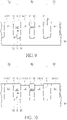
- FIG. 1 is a top view of a semiconductor structure according to an embodiment of the invention.
- FIG. 2 is a schematic cross-sectional view taken along the line I-I′ in FIG. 1 .
- FIG. 3 to FIG. 15 illustrate a method of forming a semiconductor structure.
- FIG. 1 is a top view of a semiconductor structure according to an embodiment of the present invention.
- FIG. 2 is a schematic cross-sectional view taken along the line I-I′ in FIG. 1 .
- the semiconductor structure 1 includes a substrate 100 , for example, a silicon substrate, having a first region R 1 and a second region R 2 around the first region R 1 .
- the second region R 2 may surround the first region R 1 .
- the semiconductor structure 1 may be, for example, a part of a static random access memory, wherein the first region R 1 may be the area as indicated by the dotted line.
- the first region R 1 includes at least two PMOS pull-up transistors PL 1 and PL 2 .
- the first region R 1 may be a PMOS region, that is, only PMOS transistors are provided in the first region R 1
- the second region R 2 may be an NMOS region, that is, only NMOS transistors are provided in the second region R 2 .
- FIG. 1 four active regions AA 1 to AA 4 extending along the reference Y axis and four gates G 1 to G 4 extending along the reference X axis are illustrated.
- the gate G 1 crosses the active area AA 2 to form a PMOS pull-up transistor PL 1
- the gate G 2 crosses the active area AA 3 to form a PMOS pull-up transistor PL 2 .
- STI shallow trench isolation
- the semiconductor structure 1 includes at least one first fin structure F 1 disposed in the first region R 1 , and at least one second fin structure F 2 disposed in the second region R 2 .
- a first isolation trench T 1 is provided adjacent to the first fin structure F 1 .
- a first trench isolation layer IM 1 such as a silicon oxide layer, is provided in the first isolation trench T 1 .
- a second isolation trench T 2 is provided around the first region R 1 .
- the second isolation trench T 2 is located between the first fin structure F 1 and the second fin structure F 2 .
- a second trench isolation layer IM 2 such as a silicon oxide layer, is provided in the second isolation trench T 2 .
- the bottom surface S of the second isolation trench T 2 has a step height H.
- the bottom surface S of the second isolation trench T 2 includes a first surface S 1 in the first region R 1 and a second surface S 2 in the second region R 2 , and the first surface S 1 is lower than the second surface S 2 , thereby constituting the step height H at the interface between the first region R 1 and the second region R 2 .
- the step height H is about 30-100 angstroms, but it is not limited thereto.
- the top surface ST 1 of the first trench isolation layer IM 1 and the top surface ST 2 of the second trench isolation layer IM 2 are coplanar. According to an embodiment of the present invention, the top surface FST 1 of the first fin structure F 1 is lower than the top surface FST 2 of the second fin structure F 2 .
- the gate G 1 of the semiconductor structure 1 may be disposed on the first fin structure F 1 .
- a first source region SD 1 adjacent to the gate G 1 for example, a P + doped region, is provided on the first fin structure F 1 .
- a first drain region DD 1 adjacent to the gate G 1 for example, a P + doped region, is provided on the first fin structure F 1 .
- the gate G 1 , the first source region SD 1 and the first drain region DD 1 may constitute the PMOS pull-up transistor PL 1 .
- the first source region SD 1 and the first drain region DD 1 include an epitaxial SiGe layer SG 1 , which has a height h of about 5-25 nm above the top surface ST 1 of the first trench isolation layer EVIL but not limited to this.
- the distance W between the epitaxial SiGe layer SG 1 and the adjacent epitaxial SiGe layer SG 2 on the top surface ST 1 of the first trench isolation layer IM 1 is at least 20 nm, for example, between 20 and 60 nm. Therefore, the semiconductor structure 1 of the present invention can effectively avoid the short circuit problem caused by the SiGe bridge.
- the gate G 2 of the semiconductor structure 1 may be disposed on the second fin structure F 2 .
- a second source region SD 2 adjacent to the gate G 2 is provided on the second fin structure F 2 .
- a second drain region DD 2 adjacent to the gate G 2 is provided on the second fin structure F 2 .
- the gate G 2 , the second source region SD 2 and the second drain region DD 2 can constitute an NMOS transistor.
- the second source region SD 2 and the second drain region DD 2 include an epitaxial SiP layer SPE.
- FIG. 3 to FIG. 15 illustrate a method of forming a semiconductor structure.
- a substrate 100 such as a silicon substrate, is provided with a first region R 1 and a second region R 2 around the first region R 1 .
- the second region R 2 may surround the first region R 1 .
- the first region R 1 may be a PMOS region, that is, only PMOS transistors are provided in the first region R 1
- the second region R 2 may be an NMOS region, that is, only NMOS transistors are provide in the second region R 2 .
- the substrate 100 in the first region R 1 is etched to form a recess RA in the first region R 1 , and a step height RH is formed at the interface between the first region R 1 and the second region R 2 .
- the step height RH is about 30-100 angstroms, but it is not limited thereto.
- a hard mask layer HM is then deposited on the substrate 100 in a blanket manner.
- the hard mask layer HM may include a silicon nitride layer, but is not limited thereto.
- a trench isolation process is performed.
- a lithographic process and an etching process may be performed to etch the hard mask layer HM and the substrate 100 in the predetermined area, and a first isolation trench T 1 is formed in the first area R 1 , and a second isolation trench T 2 is formed around the first area R 1 .
- at least one first fin structure F 1 is formed in the first region R 1
- at least one second fin structure F 2 is formed in the second region R 2 .
- the second isolation trench T 2 is located between the first fin structure F 1 and the second fin structure F 2 .
- Between two fin-like structures F 2 for example, the top surface FST 1 of the first fin structure F 1 is lower than the top surface FST 2 of the second fin structure F 2 by about 30-100 angstroms.
- the bottom surface S of the second isolation trench T 2 has a step height H.
- the bottom surface S of the second isolation trench T 2 includes a first surface S 1 in the first region R 1 and a second surface S 2 in the second region R 2 , and the first surface S 1 is lower than the first surface S 1 , thereby forming a step height H at the interface between the first region R 1 and the second region R 2 .
- the step height H is about 30-100 angstroms, but it is not limited thereto.
- a chemical vapor deposition (CVD) process is then performed to deposit an insulating layer 102 , such as a silicon oxide layer, on the substrate 100 in a blanket manner.
- the insulating layer 102 covers the hard mask layer HM, and fills the first isolation trench T 1 and the second isolation trench T 2 .
- the insulating layer 102 is then subjected to a planarization process, for example, a chemical mechanical polishing (CMP) process, to polish the insulating layer 102 until the top surface of the hard mask layer HM in the second region R 2 is first exposed. At this point, the top surface of the hard mask layer HM in the first region R 1 may still be covered by the insulating layer 102 .
- CMP chemical mechanical polishing
- an etch-back process is then performed, using dry etching or wet etching to etch away the insulating layer 102 of a predetermined thickness, revealing the top surface of the hard mask layer HM in the first region R 1 , so that a first trench isolation layer IM 1 is formed in the first isolation trench T 1 , and a second trench isolation layer IM 2 is formed in the second isolation trench T 2 .
- the top surface ST 1 of the first trench isolation layer IM 1 and the top surface ST 2 of the second trench isolation layer IM 2 are coplanar.
- an etching process such as wet etching, is then used to remove the hard mask layer HM to reveal the top surface FST 1 of the first fin structure F 1 and the top surface FST 2 of the second fin structure F 2 .
- the top surface ST 1 of the first trench isolation layer IM 1 and the top surface ST 2 of the second trench isolation layer IM 2 are higher than the top surface FST 2 of the second fin structure F 2
- the top surface FST 2 of the second fin structure F 2 is higher than the top surface FST 1 of the first fin structure F 1
- the height difference ht between the top surface FST 2 of the second fin structure F 2 and the top surface FST 1 of the first fin structure F 1 is about 30-100 angstroms, but is not limited thereto.
- an ion implantation process is then performed to form ion wells, such as P-type wells or N-type wells (not shown) in the substrate 100 .
- a cleaning process is performed. The above cleaning process may consume part of the thickness of the first trench isolation layer IM 1 and the second trench isolation layer IM 2 , so that the top surface ST 1 of the first trench isolation layer IM 1 and the top surface ST 2 of the second trench isolation layer IM 2 will be closer to the top surface FST 2 of the second fin structure F 2 , but still higher than the top surface FST 1 of the first fin structure F 1 .
- the height difference ht between the top surface ST 1 of the first trench isolation layer IM 1 and the top surface FST 1 of the first fin structure F 1 is about 30-100 angstroms, but is not limited thereto.
- the upper corners of the first trench isolation layer IM 1 will be rounded.
- an oxidation process is then performed to form a gate oxide layer GOX 1 and a gate oxide layer GOX 2 on the top surface FST 1 of the first fin structure F 1 and the top surface FST 2 of the second fin structure F 2 , respectively.
- the gate oxide layer GOX 1 and the gate oxide layer GOX 2 may include silicon oxide layers, but are not limited thereto.
- the gate oxide layer GOX 1 and the gate oxide layer GOX 2 may be formed of the same material.
- the gate oxide layer GOX 1 and the gate oxide layer GOX 2 may be formed of different materials.
- a polysilicon layer POL is then deposited on the substrate 100 in a blanket manner.
- the polysilicon layer POL is patterned by using a lithographic process and an etching processes to form a gate G 1 on the first fin structure F 1 and a gate G 2 on the second fin structure F 2 (as shown in FIG. 1 ). Since the polysilicon layer POL on this cross-section is removed, only the outline of the gate G 2 is shown by dotted lines in the figure. Subsequently, spacers (not shown) can be formed on the gate G 1 and the gate G 2 .
- a recessed region RE 1 and a recessed region RE 2 adjacent to the gate G 1 are then formed on the first fin structures F 1 in the first region R 1 .
- the method of forming the recessed region RE 1 and the recessed region RE 2 on the first fin structures F 1 may comprise wet etching, but is not limited thereto.
- the recessed region RE 1 and the recessed region RE 2 are separated by the first trench isolation layer IM 1 .
- the top surface ST 1 of the first trench isolation layer IM 1 and the top surface ST 2 of the second trench isolation layer IM 2 are still coplanar.
- an epitaxial process is then performed to form an epitaxial SiGe layer SG 1 and an epitaxial SiGe layer SG 2 in the recessed region RE 1 and the recessed region RE 2 in the first region R 1 , respectively.
- the epitaxial SiGe layer SG 1 and the epitaxial SiGe layer SG 2 can be formed by an organometallic vapor phase epitaxy method, but are not limited thereto.
- the second region R 2 can be masked.
- the distance W between the epitaxial SiGe layer SG 1 and the adjacent epitaxial SiGe layer SG 2 on the top surface ST 1 of the first trench isolation layer IM 1 is at least 20 nm, for example, between 20 and 60 nm. Therefore, the semiconductor structure 1 of the present invention can effectively avoid the short circuit problem caused by the SiGe bridge.
- the epitaxy process is performed to form an epitaxial SiP layer SPE on the second fin structure F 2 in the second region R 2 .
Abstract
Description
Claims (18)
Applications Claiming Priority (2)
| Application Number | Priority Date | Filing Date | Title |
|---|---|---|---|
| CN202110047083.XA CN114765171A (en) | 2021-01-14 | 2021-01-14 | Semiconductor structure and manufacturing method thereof |
| CN202110047083.X | 2021-01-14 |
Publications (2)
| Publication Number | Publication Date |
|---|---|
| US20220223720A1 US20220223720A1 (en) | 2022-07-14 |
| US11515404B2 true US11515404B2 (en) | 2022-11-29 |
Family
ID=82323328
Family Applications (1)
| Application Number | Title | Priority Date | Filing Date |
|---|---|---|---|
| US17/160,427 Active 2041-03-06 US11515404B2 (en) | 2021-01-14 | 2021-01-28 | Semiconductor structure comprising regions having an isolation trench with a stepped bottom surface therebetween and method of forming the same |
Country Status (2)
| Country | Link |
|---|---|
| US (1) | US11515404B2 (en) |
| CN (1) | CN114765171A (en) |
Families Citing this family (1)
| Publication number | Priority date | Publication date | Assignee | Title |
|---|---|---|---|---|
| US20220301922A1 (en) * | 2021-03-19 | 2022-09-22 | Taiwan Semiconductor Manufacturing Company, Ltd. | Etch profile control of isolation trench |
Citations (12)
| Publication number | Priority date | Publication date | Assignee | Title |
|---|---|---|---|---|
| KR101153158B1 (en) | 2010-03-01 | 2012-07-03 | 타이완 세미콘덕터 매뉴팩쳐링 컴퍼니 리미티드 | Dual epitaxial process for a finfet device |
| US20160211168A1 (en) * | 2015-01-21 | 2016-07-21 | Sunhom Steve Paak | Semiconductor Devices Including Active Patterns Having Different Pitches and Methods of Fabricating the Same |
| US9443962B2 (en) | 2012-11-09 | 2016-09-13 | Taiwan Semiconductor Manufacturing Company, Ltd. | Recessing STI to increase fin height in fin-first process |
| US9595611B2 (en) | 2013-08-01 | 2017-03-14 | Samsung Electronics Co., Ltd. | FinFET with a single contact to multiple fins bridged together to form a source/drain region of the transistor |
| US9735158B2 (en) | 2014-05-13 | 2017-08-15 | Samsung Electronics Co., Ltd. | Semiconductor devices having bridge layer and methods of manufacturing the same |
| US9793174B1 (en) | 2016-08-05 | 2017-10-17 | United Microelectronics Corp. | FinFET device on silicon-on-insulator and method of forming the same |
| US20180342607A1 (en) * | 2017-05-24 | 2018-11-29 | Semiconductor Manufacturing International (Shanghai) Corporation | Semiconductor structure and fabrication method thereof |
| US20190097056A1 (en) * | 2017-09-28 | 2019-03-28 | Taiwan Semiconductor Manufacturing Co., Ltd. | Semiconductor device having fins and method of fabricating the same |
| US10541253B2 (en) | 2017-01-10 | 2020-01-21 | International Business Machines Corporation | FinFETs with various fin height |
| US20200194440A1 (en) * | 2018-12-14 | 2020-06-18 | Qualcomm Incorporated | Sram source-drain structure |
| US20210265224A1 (en) * | 2020-02-26 | 2021-08-26 | Taiwan Semiconductor Manufacturing Co., Ltd. | Semiconductor Device with Dual Isolation Liner and Method of Forming the Same |
| US20210313181A1 (en) * | 2020-04-01 | 2021-10-07 | Taiwan Semiconductor Manufacturing Company, Ltd. | Cut metal gate refill with void |
-
2021
- 2021-01-14 CN CN202110047083.XA patent/CN114765171A/en active Pending
- 2021-01-28 US US17/160,427 patent/US11515404B2/en active Active
Patent Citations (12)
| Publication number | Priority date | Publication date | Assignee | Title |
|---|---|---|---|---|
| KR101153158B1 (en) | 2010-03-01 | 2012-07-03 | 타이완 세미콘덕터 매뉴팩쳐링 컴퍼니 리미티드 | Dual epitaxial process for a finfet device |
| US9443962B2 (en) | 2012-11-09 | 2016-09-13 | Taiwan Semiconductor Manufacturing Company, Ltd. | Recessing STI to increase fin height in fin-first process |
| US9595611B2 (en) | 2013-08-01 | 2017-03-14 | Samsung Electronics Co., Ltd. | FinFET with a single contact to multiple fins bridged together to form a source/drain region of the transistor |
| US9735158B2 (en) | 2014-05-13 | 2017-08-15 | Samsung Electronics Co., Ltd. | Semiconductor devices having bridge layer and methods of manufacturing the same |
| US20160211168A1 (en) * | 2015-01-21 | 2016-07-21 | Sunhom Steve Paak | Semiconductor Devices Including Active Patterns Having Different Pitches and Methods of Fabricating the Same |
| US9793174B1 (en) | 2016-08-05 | 2017-10-17 | United Microelectronics Corp. | FinFET device on silicon-on-insulator and method of forming the same |
| US10541253B2 (en) | 2017-01-10 | 2020-01-21 | International Business Machines Corporation | FinFETs with various fin height |
| US20180342607A1 (en) * | 2017-05-24 | 2018-11-29 | Semiconductor Manufacturing International (Shanghai) Corporation | Semiconductor structure and fabrication method thereof |
| US20190097056A1 (en) * | 2017-09-28 | 2019-03-28 | Taiwan Semiconductor Manufacturing Co., Ltd. | Semiconductor device having fins and method of fabricating the same |
| US20200194440A1 (en) * | 2018-12-14 | 2020-06-18 | Qualcomm Incorporated | Sram source-drain structure |
| US20210265224A1 (en) * | 2020-02-26 | 2021-08-26 | Taiwan Semiconductor Manufacturing Co., Ltd. | Semiconductor Device with Dual Isolation Liner and Method of Forming the Same |
| US20210313181A1 (en) * | 2020-04-01 | 2021-10-07 | Taiwan Semiconductor Manufacturing Company, Ltd. | Cut metal gate refill with void |
Also Published As
| Publication number | Publication date |
|---|---|
| CN114765171A (en) | 2022-07-19 |
| US20220223720A1 (en) | 2022-07-14 |
Similar Documents
| Publication | Publication Date | Title |
|---|---|---|
| US10510884B2 (en) | Method for fabricating a semiconductor device | |
| US7176084B2 (en) | Self-aligned conductive spacer process for sidewall control gate of high-speed random access memory | |
| KR100642754B1 (en) | Semiconductor device having etch resistant L shape spacer and fabrication method thereof | |
| US8790991B2 (en) | Method and structure for shallow trench isolation to mitigate active shorts | |
| US8962430B2 (en) | Method for the formation of a protective dual liner for a shallow trench isolation structure | |
| US20070170511A1 (en) | Method for fabricating a recessed-gate mos transistor device | |
| US20190013204A1 (en) | Method of fabricating buried word line and gate on finfet | |
| US11515404B2 (en) | Semiconductor structure comprising regions having an isolation trench with a stepped bottom surface therebetween and method of forming the same | |
| US10347541B1 (en) | Active gate contacts and method of fabrication thereof | |
| US20200083363A1 (en) | Oxide spacer in a contact over active gate finfet and method of production thereof | |
| US10580684B2 (en) | Self-aligned single diffusion break for fully depleted silicon-on-insulator and method for producing the same | |
| US20130146966A1 (en) | Semiconductor structure with enhanced cap and fabrication method thereof | |
| US11903193B2 (en) | Two dimensional structure to control flash operation and methods for forming the same | |
| CN112687622B (en) | Single diffusion region cutting structure of fin field effect transistor and forming method thereof | |
| US10707225B2 (en) | Semiconductor memory device and fabrication method thereof | |
| US10186524B2 (en) | Fully depleted silicon-on-insulator (FDSOI) transistor device and self-aligned active area in FDSOI bulk exposed regions | |
| US11699730B2 (en) | Semiconductor memory device and fabrication method thereof | |
| CN111477590B (en) | Grid manufacturing method | |
| CN113223948B (en) | Method for forming self-aligned metal silicide | |
| KR100481987B1 (en) | (Method for fabricating MOS capacitor of semiconductor device | |
| CN110707086B (en) | Semiconductor device with a plurality of semiconductor chips | |
| US10141194B1 (en) | Manufacturing method of semiconductor structure | |
| KR100266028B1 (en) | Semiconductor device and method for fabricating the same | |
| KR20090000461A (en) | Semiconductor device and manufacturing method thereof |
Legal Events
| Date | Code | Title | Description |
|---|---|---|---|
| AS | Assignment |
Owner name: UNITED MICROELECTRONICS CORP., TAIWAN Free format text: ASSIGNMENT OF ASSIGNORS INTEREST;ASSIGNORS:YANG, TSUNG-YU;LI, SHIN-HUNG;TSAO, RUEI-JHE;AND OTHERS;REEL/FRAME:055070/0673 Effective date: 20201230 |
|
| FEPP | Fee payment procedure |
Free format text: ENTITY STATUS SET TO UNDISCOUNTED (ORIGINAL EVENT CODE: BIG.); ENTITY STATUS OF PATENT OWNER: LARGE ENTITY |
|
| STPP | Information on status: patent application and granting procedure in general |
Free format text: RESPONSE TO NON-FINAL OFFICE ACTION ENTERED AND FORWARDED TO EXAMINER |
|
| STPP | Information on status: patent application and granting procedure in general |
Free format text: NOTICE OF ALLOWANCE MAILED -- APPLICATION RECEIVED IN OFFICE OF PUBLICATIONS |
|
| STPP | Information on status: patent application and granting procedure in general |
Free format text: PUBLICATIONS -- ISSUE FEE PAYMENT VERIFIED |
|
| STCF | Information on status: patent grant |
Free format text: PATENTED CASE |