US11474343B2 - Tunable MEMS etalon device - Google Patents
Tunable MEMS etalon device Download PDFInfo
- Publication number
- US11474343B2 US11474343B2 US16/461,808 US201716461808A US11474343B2 US 11474343 B2 US11474343 B2 US 11474343B2 US 201716461808 A US201716461808 A US 201716461808A US 11474343 B2 US11474343 B2 US 11474343B2
- Authority
- US
- United States
- Prior art keywords
- mirror
- gap
- actuated
- tunable etalon
- etalon device
- Prior art date
- Legal status (The legal status is an assumption and is not a legal conclusion. Google has not performed a legal analysis and makes no representation as to the accuracy of the status listed.)
- Active, expires
Links
- BJQHLKABXJIVAM-UHFFFAOYSA-N bis(2-ethylhexyl) phthalate Chemical compound CCCCC(CC)COC(=O)C1=CC=CC=C1C(=O)OCC(CC)CCCC BJQHLKABXJIVAM-UHFFFAOYSA-N 0.000 title claims abstract description 124
- 239000011521 glass Substances 0.000 claims abstract description 46
- 125000006850 spacer group Chemical group 0.000 claims abstract description 23
- 239000010410 layer Substances 0.000 claims description 75
- 239000000463 material Substances 0.000 claims description 38
- 238000003384 imaging method Methods 0.000 claims description 20
- 229910052710 silicon Inorganic materials 0.000 claims description 16
- 239000010703 silicon Substances 0.000 claims description 16
- 230000007246 mechanism Effects 0.000 claims description 11
- 239000012780 transparent material Substances 0.000 claims description 11
- 239000002356 single layer Substances 0.000 claims description 5
- 239000012212 insulator Substances 0.000 claims description 3
- 230000003595 spectral effect Effects 0.000 description 37
- 235000012431 wafers Nutrition 0.000 description 37
- 230000003287 optical effect Effects 0.000 description 21
- 230000005540 biological transmission Effects 0.000 description 20
- XUIMIQQOPSSXEZ-UHFFFAOYSA-N Silicon Chemical compound [Si] XUIMIQQOPSSXEZ-UHFFFAOYSA-N 0.000 description 15
- 238000000034 method Methods 0.000 description 15
- 230000005496 eutectics Effects 0.000 description 11
- 238000004519 manufacturing process Methods 0.000 description 10
- 238000006073 displacement reaction Methods 0.000 description 9
- 239000000758 substrate Substances 0.000 description 9
- 230000008569 process Effects 0.000 description 7
- 239000000725 suspension Substances 0.000 description 7
- 239000011248 coating agent Substances 0.000 description 6
- 238000000576 coating method Methods 0.000 description 6
- 238000001914 filtration Methods 0.000 description 6
- 229910052751 metal Inorganic materials 0.000 description 6
- 239000002184 metal Substances 0.000 description 6
- 239000004033 plastic Substances 0.000 description 6
- 239000006117 anti-reflective coating Substances 0.000 description 5
- 230000008901 benefit Effects 0.000 description 5
- 239000003086 colorant Substances 0.000 description 5
- 229910052732 germanium Inorganic materials 0.000 description 5
- GNPVGFCGXDBREM-UHFFFAOYSA-N germanium atom Chemical compound [Ge] GNPVGFCGXDBREM-UHFFFAOYSA-N 0.000 description 5
- 238000000701 chemical imaging Methods 0.000 description 3
- 238000004891 communication Methods 0.000 description 3
- 238000005516 engineering process Methods 0.000 description 3
- 230000010354 integration Effects 0.000 description 3
- 229910021421 monocrystalline silicon Inorganic materials 0.000 description 3
- VYPSYNLAJGMNEJ-UHFFFAOYSA-N Silicium dioxide Chemical compound O=[Si]=O VYPSYNLAJGMNEJ-UHFFFAOYSA-N 0.000 description 2
- GWEVSGVZZGPLCZ-UHFFFAOYSA-N Titan oxide Chemical compound O=[Ti]=O GWEVSGVZZGPLCZ-UHFFFAOYSA-N 0.000 description 2
- 238000005452 bending Methods 0.000 description 2
- 230000015572 biosynthetic process Effects 0.000 description 2
- 230000007423 decrease Effects 0.000 description 2
- 238000000708 deep reactive-ion etching Methods 0.000 description 2
- 238000010586 diagram Methods 0.000 description 2
- 238000005530 etching Methods 0.000 description 2
- 230000035939 shock Effects 0.000 description 2
- 238000005476 soldering Methods 0.000 description 2
- 238000001228 spectrum Methods 0.000 description 2
- 229910003086 Ti–Pt Inorganic materials 0.000 description 1
- 230000004075 alteration Effects 0.000 description 1
- 238000003491 array Methods 0.000 description 1
- 239000003990 capacitor Substances 0.000 description 1
- 230000008859 change Effects 0.000 description 1
- 229910052802 copper Inorganic materials 0.000 description 1
- 238000013016 damping Methods 0.000 description 1
- 230000003247 decreasing effect Effects 0.000 description 1
- 238000000151 deposition Methods 0.000 description 1
- 230000008021 deposition Effects 0.000 description 1
- 230000008713 feedback mechanism Effects 0.000 description 1
- 229910052737 gold Inorganic materials 0.000 description 1
- 238000002513 implantation Methods 0.000 description 1
- 239000002346 layers by function Substances 0.000 description 1
- 239000012528 membrane Substances 0.000 description 1
- 238000001465 metallisation Methods 0.000 description 1
- 238000002156 mixing Methods 0.000 description 1
- 238000004806 packaging method and process Methods 0.000 description 1
- 238000000059 patterning Methods 0.000 description 1
- 238000002310 reflectometry Methods 0.000 description 1
- 238000000926 separation method Methods 0.000 description 1
- 239000000377 silicon dioxide Substances 0.000 description 1
- 229910000679 solder Inorganic materials 0.000 description 1
- 230000003068 static effect Effects 0.000 description 1
- OGIDPMRJRNCKJF-UHFFFAOYSA-N titanium oxide Inorganic materials [Ti]=O OGIDPMRJRNCKJF-UHFFFAOYSA-N 0.000 description 1
- 238000000411 transmission spectrum Methods 0.000 description 1
- 238000010200 validation analysis Methods 0.000 description 1
Images


Classifications
-
- G—PHYSICS
- G02—OPTICS
- G02B—OPTICAL ELEMENTS, SYSTEMS OR APPARATUS
- G02B26/00—Optical devices or arrangements for the control of light using movable or deformable optical elements
- G02B26/007—Optical devices or arrangements for the control of light using movable or deformable optical elements the movable or deformable optical element controlling the colour, i.e. a spectral characteristic, of the light
-
- G—PHYSICS
- G02—OPTICS
- G02B—OPTICAL ELEMENTS, SYSTEMS OR APPARATUS
- G02B26/00—Optical devices or arrangements for the control of light using movable or deformable optical elements
- G02B26/001—Optical devices or arrangements for the control of light using movable or deformable optical elements based on interference in an adjustable optical cavity
-
- B—PERFORMING OPERATIONS; TRANSPORTING
- B81—MICROSTRUCTURAL TECHNOLOGY
- B81B—MICROSTRUCTURAL DEVICES OR SYSTEMS, e.g. MICROMECHANICAL DEVICES
- B81B3/00—Devices comprising flexible or deformable elements, e.g. comprising elastic tongues or membranes
- B81B3/0035—Constitution or structural means for controlling the movement of the flexible or deformable elements
- B81B3/0056—Adjusting the distance between two elements, at least one of them being movable, e.g. air-gap tuning
-
- G—PHYSICS
- G01—MEASURING; TESTING
- G01J—MEASUREMENT OF INTENSITY, VELOCITY, SPECTRAL CONTENT, POLARISATION, PHASE OR PULSE CHARACTERISTICS OF INFRARED, VISIBLE OR ULTRAVIOLET LIGHT; COLORIMETRY; RADIATION PYROMETRY
- G01J3/00—Spectrometry; Spectrophotometry; Monochromators; Measuring colours
- G01J3/12—Generating the spectrum; Monochromators
- G01J3/26—Generating the spectrum; Monochromators using multiple reflection, e.g. Fabry-Perot interferometer, variable interference filters
-
- G—PHYSICS
- G01—MEASURING; TESTING
- G01J—MEASUREMENT OF INTENSITY, VELOCITY, SPECTRAL CONTENT, POLARISATION, PHASE OR PULSE CHARACTERISTICS OF INFRARED, VISIBLE OR ULTRAVIOLET LIGHT; COLORIMETRY; RADIATION PYROMETRY
- G01J3/00—Spectrometry; Spectrophotometry; Monochromators; Measuring colours
- G01J3/28—Investigating the spectrum
- G01J3/2823—Imaging spectrometer
-
- G—PHYSICS
- G01—MEASURING; TESTING
- G01J—MEASUREMENT OF INTENSITY, VELOCITY, SPECTRAL CONTENT, POLARISATION, PHASE OR PULSE CHARACTERISTICS OF INFRARED, VISIBLE OR ULTRAVIOLET LIGHT; COLORIMETRY; RADIATION PYROMETRY
- G01J3/00—Spectrometry; Spectrophotometry; Monochromators; Measuring colours
- G01J3/28—Investigating the spectrum
- G01J3/30—Measuring the intensity of spectral lines directly on the spectrum itself
- G01J3/32—Investigating bands of a spectrum in sequence by a single detector
-
- G—PHYSICS
- G01—MEASURING; TESTING
- G01J—MEASUREMENT OF INTENSITY, VELOCITY, SPECTRAL CONTENT, POLARISATION, PHASE OR PULSE CHARACTERISTICS OF INFRARED, VISIBLE OR ULTRAVIOLET LIGHT; COLORIMETRY; RADIATION PYROMETRY
- G01J3/00—Spectrometry; Spectrophotometry; Monochromators; Measuring colours
- G01J3/46—Measurement of colour; Colour measuring devices, e.g. colorimeters
- G01J3/50—Measurement of colour; Colour measuring devices, e.g. colorimeters using electric radiation detectors
- G01J3/51—Measurement of colour; Colour measuring devices, e.g. colorimeters using electric radiation detectors using colour filters
-
- G—PHYSICS
- G02—OPTICS
- G02B—OPTICAL ELEMENTS, SYSTEMS OR APPARATUS
- G02B5/00—Optical elements other than lenses
- G02B5/20—Filters
- G02B5/28—Interference filters
- G02B5/284—Interference filters of etalon type comprising a resonant cavity other than a thin solid film, e.g. gas, air, solid plates
-
- B—PERFORMING OPERATIONS; TRANSPORTING
- B81—MICROSTRUCTURAL TECHNOLOGY
- B81B—MICROSTRUCTURAL DEVICES OR SYSTEMS, e.g. MICROMECHANICAL DEVICES
- B81B2201/00—Specific applications of microelectromechanical systems
- B81B2201/04—Optical MEMS
- B81B2201/042—Micromirrors, not used as optical switches
Definitions
- the presently disclosed subject matter relates generally to Micro-Electro-Mechanical systems (MEMS) and more particularly to tunable MEMS-based spectral filters.
- MEMS Micro-Electro-Mechanical systems
- Color imaging is known and performed in general using digital cameras having pixelated image sensors covered with color filter arrays (CFAs), for example Bayer-type CFAs.
- CFAs color filter arrays
- Recently, systems and methods for color imaging using sequential imaging have been proposed, see e.g. co-assigned international patent application publication WO 2014/207742. Such systems and methods allow capture of colorful images with improved color fidelity and/or with hyper spectral color information.
- sequential imaging utilizes a tunable spectral filter placed along a line of sight of the camera image sensor.
- the image sensor is operated to acquire a series of images in a short time sequence while the spectral transmission of the tunable spectral filter is varied. Accordingly each image of the series corresponds to a different color content of the captured scene, in accordance with the state/profile of spectral transmission of the filter set when the respective image was taken.
- An example of a tunable spectral filter that can be used for sequential imaging as above is an etalon.
- An etalon comprises two parallel mirrors. The spectral transmission profile is determined by the gap between the mirrors. The tuning of a voltage applied to etalon tunes the gap between the mirrors (which provides a so called “optical cavity”) and, in turn, tunes the spectral transmission profile.
- the two mirrors may be for example a semi-transparent front mirror and a semi-transparent back mirror.
- the back mirror may be, for example, stationary while the front mirror may be movable toward/away from the back mirror in order to change the distance (optical cavity) between them, and thereby tune the spectral transmission profile.
- Etalons are widely used in optical communication to filter, modulate and/or control the properties of optical signals, such as laser light beams, transmitted along the optical communication channels. Yet when considering optical communication, often the filter is required to operate accurately and efficiently in only a limited spectral band (e.g. of several nanometers), and is not required to provide specific/wide transmission profiles as in many cases required for sequential spectral imaging applications (see e.g. WO 2014/207742).
- a limited spectral band e.g. of several nanometers
- regular (e.g. RGB) color image data acquisition, IR image data acquisition and/or high spectral imaging not only is the etalon often required to have a wide spectral transmission profile and wide free spectral range (which may impose a short distance between the etalon mirrors), but also it may be required to be laterally wide enough so as to cover the entire field of view of the image sensor in front of which it is positioned.
- tunable etalons for use in sequential spectral color imaging have often very high aspect ratio between their width and the distance between their mirrors.
- the displacement/gap and parallelism between the front mirror and the back mirror may be adjusted by applying electric potential difference between two or more regions of electrodes formed on an actuation layer (including for example, the actuation substrate carrying the actuation mechanism, being part of the functional mechanical layer) which are substantially electrically insulated from one another, and an approximately parallel set of electrodes formed on a functional mechanical layer to thereby cause electrostatic forces between them.
- the functional layer is considered here as the layer which experiences a displacement upon applying the actuation force.
- the electrodes are formed in the handle layer of a silicon-on-insulator (SOI) wafer, they may be electrically insulated from one another by trenches in the layer.
- SOI silicon-on-insulator
- Embodiments disclosed herein teach several tunable MEMS etalon architectures and actuation paradigms.
- a common feature in all the embodiments is that the front mirror (of the two mirrors the one facing incoming light) is attached to a MEMS functional mechanical layer.
- MEMS actuators allows low-cost mass fabrication of the proposed etalons and renders them suitable for implementation in consumer electronics devices.
- attachment of the front mirror to the functional mechanical layer is done by pick and place technique as known in the art.
- the method according to this aspect of the presently disclosed subject matter can optionally comprise one or more of features (i) to (xix) listed below, in any technically possible combination or permutation:
- a tunable etalon device comprising a front mirror and a back mirror, the front and back mirrors separated in an initial un-actuated etalon state by a gap having a pre-stressed un-actuated gap size, the etalon configured to assume at least one actuated state in which the gap has an actuated gap size greater than the pre-stressed un-actuated gap size.
- the presently disclosed subject matter can further comprise one or more of features (i) to (xxxiv) listed below, in any technically possible combination or permutation:
- the pre-stressed un-actuated gap size is determined by a back stopper structure in physical contact with the front and back mirrors.
- the back stopper structure may be formed initially on either mirror.
- the tunable etalon devices disclosed herein are fabricated using MEMS technologies and are therefore also referred to as tunable MEMS etalon devices.
- the tunable etalon device disclosed herein further comprises an anchor structure, a frame structure fixedly coupled to the front mirror, and a flexure structure attached to the anchor structure and to the frame structure but not attached to the front mirror.
- the tunable etalon device disclosed herein further comprises a spacer structure separating the anchor structure from the back mirror, and wherein the front mirror and the spacer structure are formed in a same single layer.
- the back mirror is included in a layer made of a transparent or semi-transparent material.
- the transparent or semi-transparent material can be anyone of the following materials: glass; plastic; silicon; and germanium.
- the transparent or semi-transparent layer further includes a recess for assisting in pre-stressing the flexure structure to enhance the pre-stressed un-actuated state.
- the anchor structure, the frame structure and the flexure structure are made of silicon (Si).
- the tunable etalon device wherein the anchor structure, the frame structure and the flexure structure are formed in a same single layer.
- the tunable etalon device wherein the single layer is made of anyone of the following materials: glass; plastic; silicon; and germanium.
- the tunable etalon device wherein the back mirror is integrated in a layer made of a transparent or semi-transparent material (including for example: anyone of the following materials: glass; plastic; silicon; and germanium.
- a transparent or semi-transparent material including for example: anyone of the following materials: glass; plastic; silicon; and germanium.
- the tunable etalon device wherein the back mirror is included in a hybrid structure comprising a combination of at least two materials wherein a first material of the at least two materials is transparent or semi-transparent, and a second material of the at least two materials is stiffer than the first material.
- the tunable etalon device wherein the different materials include for example glass and silicon.
- the tunable etalon device further comprising a cap plate located at object side relative to the front mirror.
- the tunable etalon device further comprising a front stopper structure that determines a minimal gap between the front mirror and a cap plate.
- the tunable etalon device wherein the cap plate accommodates at least part of an actuation mechanism configured for controlling a gap size between the front mirror and the back mirror.
- the tunable etalon device wherein the cap plate includes at least one first electrode formed on a cap surface facing the frame structure, wherein the frame structure is configured to act as a second electrode, and wherein the frame structure is movable by electrostatic actuation using the first and second electrodes.
- the tunable etalon device wherein the at least one first electrode includes a plurality of electrodes insulated electrically from each other.
- the tunable etalon device further comprising a front stopper structure that determines a minimal electrostatic gap between the frame structure and the at least one first electrode.
- the tunable etalon device wherein the cap plate includes a transparent or semi-transparent material, thereby providing a tunable etalon enclosed between two transparent or semi-transparent plates.
- the tunable etalon device further comprising a Si layer serving as the at least one first electrode, wherein the frame structure is configured to act as a second electrode, and wherein the frame structure is movable by electrostatic actuation using the first and second electrodes.
- the tunable etalon device wherein the Si layer is a handle layer of a silicon-on-insulator (SOT) wafer, the device being an “SOT device”.
- SOT silicon-on-insulator
- the tunable etalon device wherein the at least one first electrode includes a plurality of first electrodes formed in the handle layer of the SOT wafer, the first electrodes connected mechanically and insulated electrically from each other.
- the tunable etalon device further comprising a buried oxide (BOX) layer separating the Si layer from the frame structure, the BOX layer having a thickness that determines an electrostatic gap between the front mirror and the first electrode in the pre-stressed un-actuated device state.
- BOX buried oxide
- the tunable etalon device further comprising an opening in the handle layer of the SOT wafer to allow light passage to the front and back mirrors.
- the tunable etalon device further comprising a first lens integrated with the back mirror and a second lens integrated with the cap.
- the tunable etalon device of any of claims 19 - 22 or 24 - 27 further comprising a respective lens integrated with each of the front and back mirrors.
- the tunable etalon device of any of claims 19 - 22 or 24 - 27 further comprising a respective lens integrated with the back mirror and the cap.
- the tunable etalon device of claim 25 wherein the actuated gap size between the front mirror and the back mirror is defined by front stoppers that separate between a frame structure and a cap.
- the actuation mechanism includes a piezoelectric actuator.
- the actuation mechanism includes Kelvin force actuation electrodes.
- the tunable etalon device of any one of claims is designed to assume one of a first state and a second state, wherein the gap in each of the first and the second state allows light in a certain wavelength range to pass through the etalon; wherein the first state is the initial pre-stressed un-actuated state having an un-actuated gap size between the front mirror and the back mirror, which is defined by the back stoppers; and the second state is an actuated state in which the gap size between the front mirror and the back mirror has an actuated gap size greater than the pre-stressed un-actuated gap size.
- actuated gap size between the front mirror and the back mirror is defined by front stoppers.
- an imaging device comprising:
- a tunable etalon device comprising a front mirror and a back mirror, the front and back mirrors separated in an initial pre-stressed un-actuated state by a gap having a pre-stressed un-actuated gap size, the etalon configured to assume at least one actuated state in which the gap has an actuated gap size gap greater than the pre-stressed un-actuated gap size;
- a controller configured and operable to tune the tunable etalon device and to capture image data through the image sensor.
- the imaging device accordance with the presently disclosed subject matter can optionally comprise one or more of features (i) to (xxxiv) listed above, mutatis mutandis, in any desired combination or permutation.
- FIG. 1A shows schematically in an isomeric view a tunable MEMS etalon device, according to an example of the presently disclosed subject matter
- FIG. 1B shows schematically the device of FIG. 1A with a cross section, according to an example of the presently disclosed subject matter
- FIG. 2A shows the device of FIG. 1B in an initial as-fabricated, non-stressed un-actuated state, according to an example of the presently disclosed subject matter
- FIG. 2B shows the device of FIG. 2A in an initial pre-stressed un-actuated state, according to an example of the presently disclosed subject matter
- FIG. 2C shows the device of FIG. 2B in an actuated state, according to an example of the presently disclosed subject matter
- FIG. 3 shows schematically a top view of the functional mechanical layer in the device of FIG. 1A or FIG. 1B , according to an example of the presently disclosed subject matter;
- FIG. 4 shows schematically a top view of the cap in the device of FIG. 1A or FIG. 1B with multiple electrodes formed thereon, according to an example of the presently disclosed subject matter;
- FIG. 5A shows schematically a tunable MEMS etalon device, in a cross-sectional view and in an initial as-fabricated, non-stressed un-actuated state, according to another example of the presently disclosed subject matter;
- FIG. 5B shows the device of FIG. 5A in an initial pre-stressed un-actuated state, according to an example of the presently disclosed subject matter
- FIG. 5C shows the device of FIG. 5B in an actuated state, according to an example of the presently disclosed subject matter
- FIG. 6 shows a bottom view of the handle layer of the SOI wafer in the device of FIG. 5A or 5B , according to an example of the presently disclosed subject matter
- FIG. 7 shows an assembly comprising a device disclosed herein with integrated optics, according to an example of the presently disclosed subject matter
- FIG. 8 illustrates schematically in a block diagram a sequential imaging system configured according to an example of the presently disclosed subject matter
- FIG. 9 shows schematically stages in a fabrication process of a GSG tunable MEMS etalon device disclosed herein, according to an example of the presently disclosed subject matter
- FIG. 10A shows schematically a tunable MEMS etalon device, in a cross-sectional view and in an initial as-fabricated, non-stressed un-actuated state, according to another example of the presently disclosed subject matter;
- FIG. 10B shows the device of FIG. 10A in an initial pre-stressed un-actuated state, according to an example of the presently disclosed subject matter.
- FIG. 10C shows the device of FIG. 10B in an actuated state, according to an example of the presently disclosed subject matter
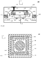
- FIG. 1A shows schematically in an isomeric view a first example of a tunable MEMS etalon device disclosed herein and numbered 100 .
- FIG. 1B shows an isomeric cross section of device 100 along a plane marked A-A.
- Device 100 is shown in conjunction with a XYZ coordinate system, which also holds for all following drawings.
- FIGS. 2A, 2B and 2C show cross sections of device 100 in plane A-A in three configurations (states): an as-fabricated (non-stressed) un-actuated state ( FIG. 2A ), a pre-stressed un-actuated state ( FIG. 2B ), and an actuated state ( FIG. 2C ).
- Device 100 comprises two substantially flat and parallel mirrors/reflective-surfaces, a bottom (or “back”) mirror 102 and a top (or “aperture”) mirror 104 separated by a “back” gap.
- a bottom (or “back”) mirror 102 and a top (or “aperture”) mirror 104 separated by a “back” gap.
- the terms “front” and “back” reflect the orientation of the device toward light rays.
- the front (top) mirror is the first mirror in the path of light rays entering the etalon.
- the mirrors are formed in flat plates or wafers made of transparent or semi-transparent material to light in a desired wavelength range transmitted by the tunable etalon filter (e.g. glass).
- the tunable etalon filter e.g. glass
- glass is used as a general non-limiting example. It is noted that the term glass should not be construed as limiting and other materials are also contemplated including any material or combination of materials with suitable transparency to light in a required wavelength range for the etalon and the image sensor to function in a desired way, for example plastic, silica, germanium, or silicon (silicon is transparent to wavelengths of roughly 1-8 ⁇ m).
- plate refers to a substantially two-dimensional structure with a thickness defined by two parallel planes and having a width and a length substantially larger that the thickness. “Layer” may also refer to a much thinner structure (down to nanometers-thick, as opposed to a typical thickness of micrometers for the other layers).
- back mirror 102 is formed in a glass layer that also serves as a substrate of the device.
- back mirror 102 may be formed in a “hybrid” plate or hybrid material such that a central section (“aperture”) through which the light rays pass is transparent to the wavelength of the light (made e.g. of a glass), while plate sections surrounding the aperture are made of a different material, for example silicon.
- the hybrid aspect may increase the stiffness and strength of the mirror.
- the back gap between the front and back mirrors has a size marked by g 0 .
- the back gap has a size marked by g 1 .
- the back gap has a size marked by g 2 .
- the mirrors are movable with respect to each other so that back gap can be tuned between certain minimal (g Mn ) and maximal (g Mx ) gap sizes. The movement is in the Z direction in the particular coordinate system shown.
- back mirror 102 facing sensor side relative to front mirror
- front mirror 104 facing object side relative to back mirror
- the maximal back gap size g Mx corresponds to a “maximal” actuated state. There are of course many actuated states (and even a continuous range of states) in which the back gap has a value g 2 between g Mn and g Mx .
- Device 100 further comprises a first stopper structure (also referred to as “back stoppers”) 106 positioned between mirrors 102 and 104 in a way such as not to block light rays designed to reach an image sensor.
- Back stoppers 106 may be formed on either mirror.
- the two mirrors are located in a close proximity to each other, the minimal gap distance g Mn being defined by back stoppers 106 which function as displacement limiters.
- An additional function of stoppers 106 is to prevent undesirable displacement of the front mirror due to external shock and vibration.
- Back stoppers 106 are designed to prevent contact between the mirrors and ensure that g Mn is never zero.
- back stoppers 106 are made of a metal such as patterned Cr—Au layer, Ti—Au layer or Ti—Pt layer.
- the degrees of reflectivity/transparency of the top and back mirrors are selected in accordance with the desired spectral transmission properties of the etalon. According to some examples, each mirror is at least semi-reflective to some degree.
- Device 100 further comprises a mounting frame structure (or simply “frame”) 108 with an opening (“aperture”) 110 .
- Frame 108 is made of a transparent or semi-transparent material (for example single crystal silicon) and is fixedly attached (e.g. by bonding) to front mirror 104 . That is, mirror 104 is “mounted” on frame 108 and therefore moves together with frame 108 . Opening 110 allows light rays to enter the etalon through the front mirror. Therefore, the front mirror is also referred to sometimes as “aperture mirror”.
- back mirror 102 and optionally front mirror 104 include a Titanium Oxide (TiO 2 ) layer deposited on a glass layer/substrate.
- a device disclosed herein may comprise one or more electrodes (not shown) formed on back mirror 102 on the surface facing frame 108 , to enable actuation of the frame structure (and thereby cause movement of the front mirror) toward the back mirror.
- Alternative actuation mechanisms may be applied, e.g. piezoelectric actuation, Kelvin force, etc.
- the movement of the front mirror towards or away from the back mirror tunes the spectral transmission band profile of the etalon.
- Device 100 further comprises an anchor structure (or simply “anchor”) 112 , made of a transparent or semi-transparent material (for example single crystal silicon).
- Anchor 112 and frame 108 are attached to each other by a flexure/suspension structure.
- the suspension structure may be for example a region of anchor structure 112 patterned in the form of a bending or torsional spring, a combination of such springs, or as a thin doughnut-shaped membrane adapted to carry the front mirror.
- the suspension structure includes a plurality of suspension springs/flexures.
- the plurality of suspension springs/flexures includes four springs, 114 a , 114 b , 114 C and 114 d , made of transparent or semi-transparent material (for example single crystal silicon. Together, frame 108 , anchor 112 and springs 114 form a “functional mechanical layer” 300 , shown in a top view in FIG. 3 .
- silicon is used as a general non-limiting example. It is noted that the term silicon should not be construed as limiting and other materials are also contemplated including any material or combination of materials with suitable flexibility and durability required for the flexure structure to function in a desired way, for example plastic or glass.
- FIGS. 2A-2C show that a surface of front mirror 104 facing incoming light is attached to frame 108 .
- a different configuration of front mirror 104 and frame 108 is described below with reference to FIG. 10 .
- a flexure structure comprising four springs 114 a , 114 b , 114 C and 114 d (see FIG. 3 ), is attached to anchor 112 and to frame structure 108 but not attached to the front mirror.
- frame 108 is spaced apart from back mirror 102 by a spacer structure (or simply “spacers”) 116 .
- spacers 116 can be formed of a glass material. Spacers 116 are used to separate the frame and springs from the plate in which mirror 102 is formed. While in principle silicon anchors 112 could be attached to the bottom plate directly without spacers 116 , this requires very large deformation of the springs. For the adopted geometry, this deformation is beyond the strength limit of the spring material, which requires the presence of spacer layer 116 .
- both movable front mirror 104 and spacers 116 are fabricated from the same glass plate (wafer). This simplifies fabrication, since the glass and silicon wafers are bonded at wafer level. For this reason, device 100 is referred to herein as a glass-silicon-glass (GSG) device.
- GSG glass-silicon-glass
- Device 100 further comprises a cap plate (or simply “cap”) 118 accommodating at least part of an actuation mechanism configured for controlling gap size between the front mirror and the back mirror.
- cap 118 is located at object side relative to front mirror 104 at the direction of incoming light.
- cap 118 accommodates electrodes 120 formed on or attached thereto (see FIGS. 2A to 2C ). Electrodes 120 can be positioned for example at a bottom side (facing the mirrors) of cap 118 . Electrodes 120 are in permanent electrical contact through one or more through-glass vias 124 with one or more bonding pads 126 positioned on the opposite (top) side of cap 118 .
- Electrodes 120 are used for actuation of frame 108 (thereby causing movement of front mirror 104 ).
- the cap comprises a first recess (cavity) 119 to provide a “front” (also referred to as “electrostatic”) gap d between frame 108 and electrodes 120 .
- gap d In the as-fabricated configuration (before the bonding of the device to the back mirror), FIG. 2A , gap d has a size d 0 .
- gap d After bonding, in the pre-stressed un-actuated state shown in FIG. 2B , gap d has a maximal size d Mx . In any actuated state (as in FIG. 2C ), gap d has a size d 2 .
- Device 100 further comprises front stoppers 122 that separate between frame 108 and cap 118 .
- front stoppers 122 isolate electrically (prevent electrical shorts between) frame 108 from cap electrodes 120 .
- front stoppers 122 defines a maximal gap between front mirror 104 and back mirror 102 .
- the cap is made of a glass material.
- cap 118 may be made of a “hybrid” plate or hybrid material such that a central section (“aperture”) through which the light rays pass is transparent to the wavelength of the light (made e.g. of a glass), while plate sections surrounding the aperture are made of a different material, for example silicon.
- the hybrid aspect may increase the stiffness and strength of the cap.
- the length L and width W ( FIG. 1A ) of mirrors 102 and 104 should on one hand be large enough (e.g. on the order of several hundred micrometers ( ⁇ m) to several millimeters (mm)) to allow light passage to a relatively wide multi-pixel image sensor.
- the minimal gap g Mn should be small enough (e.g. a few tens of nanometers (nm)) to allow desired spectral transmission properties of the etalon. This results in a large aspect ratio of the optical cavity between the mirrors (e.g.
- g Mn may have a value of down to 20 nanometers (nm), while g Mx may have a value of up to 2 ⁇ m. According to one example, the value of g Mx may be between 300 to 400 nm. Specific values depend on the required optical wavelength and are dictated by a specific application. Thus, g Mx may be greater than g Mx by one to two orders of magnitude.
- L and W may each be about 2 millimeter (mm) and springs 114 may be each about 50 ⁇ m thick, about 30 ⁇ m wide and about 1.4 mm long.
- the thicknesses of the glass layers of the cap 118 , the back mirror 102 and the front mirror 104 may be about 200 ⁇ m.
- L W.
- FIGS. 2A-2C provide additional information on the structure of device 100 as well as on the function of some of its elements.
- FIG. 2A shows device 100 in an initial as-fabricated and un-actuated, non-stressed state. As-fabricated, front mirror 104 does not touch back stoppers 106 .
- FIG. 2B shows the device of FIG. 2A in an initial pre-stressed un-actuated state, with front mirror 104 physically touching back stoppers 106 .
- the physical contact is induced by stress applied on the frame through the springs when spacer layer 116 is forced into contact with the glass wafer substrate (which includes back mirror 102 ) for eutectic bonding of spacers 116 to the glass plate of back mirror 102 , see FIG.
- FIG. 2C shows the device in an actuated state, with front mirror 104 in an intermediate position between back stoppers 106 and front stoppers 122 , moved away from back mirror 102 .
- back mirror 102 includes a second recess 128 with a depth t designed to provide pre-stress of the springs after assembly/bonding.
- recess depth t is chosen on one hand such that the contact force arising due to the deformation of the springs and the attachment of front movable mirror 104 to back stoppers 106 is high enough to preserve the contact in the case of shocks and vibrations during the normal handling of the device.
- the combined value of recess depth t plus the maximal required travel distance (maximal back gap size) g Mx is smaller than one third of an as-fabricated (“electrostatic”) gap size d 0 of a gap between electrodes 120 and frame 108 ( FIG.
- the as-fabricated electrostatic gap d 0 may have a value of about 3-4 ⁇ m and t may have a value of about 0.5-1 ⁇ m.
- the requirement for stable operation is t+g Mx ⁇ d 0 /3, since the stable travel distance of a capacitive actuator is 1 ⁇ 3 of the as-fabricated electrostatic gap, i.e. is d o /3.
- an un-actuated state may include a configuration in which movable mirror 104 is suspended and does not touch either back stoppers 106 or front stoppers 122 .
- the mounting ring and the front mirror are displaced away from the back mirror. This is achieved by applying a voltage V between the one or more regions/electrodes 120 of the actuation substrate serving as an actuating electrode and the one or more regions frame 108 .
- device 100 is fully transparent. It includes a transparent back mirror ( 102 ), a transparent front mirror ( 104 ) and a transparent cap ( 118 ) as well as transparent functional mechanical layer 300 .
- One advantage of the full transparency is that the device can be observed optically from two sides. Another advantage is that this architecture may be useful for many other optical devices incorporating movable mechanical/optical elements, such as mirrors, diffractive gratings or lenses.
- device 100 is configured as a full glass structure, where the functional mechanical layer includes a glass substrate that is pattered to accommodate/define the suspension structure carrying the top mirror, the suspension structure including a plurality of glass springs/flexures.
- FIG. 3 shows schematically a top view of functional mechanical layer 300 .
- the figure also shows an external contour 302 of front mirror 104 , aperture 110 , anchor structure 112 , springs 114 a - d (flexure structure) and a contour 304 enclosing a eutectic bond frame 121 and cap spacers 122 as further described in more detail with reference to FIG. 4 below.
- FIG. 4 shows schematically a top view of cap 118 with a plurality of electrodes 120 , marked here 120 a , 120 b , 120 c and 120 d .
- the number and shape of electrodes 120 shown are shown by way of example only and should not be construed as limiting. According to some examples, three electrodes 120 are required to control both the displacement of the frame in the Z direction and the tilting of the frame about X and Y axes.
- Multiple electrode regions e.g. as shown in FIG. 4 , may be fabricated on cap 118 such that front mirror 104 can be actuated with an up-down degree of freedom (DOF) along the Z direction and can also be tilted (e.g.
- DOF up-down degree of freedom
- cap 118 may include a deposited eutectic bonding material 121 .
- spacers 122 may be used to precisely control the electrostatic gap between the cap electrodes 120 and the actuator frame 108 serving as the second electrode.
- the eutectic bonding material 121 can be made to assume the shape of a frame. In such case, spacers 122 can be placed on both sides of the frame (inner and outer) and thereby minimize bending moments acting on the cap as a result of the eutectic bonding shrinkage during the bonding process.
- Device 100 is actuated to bring the etalon from the initial pre-stressed un-actuated state ( FIG. 2B ) to an actuated state (e.g. as in FIG. 2C ).
- the actuation moves frame 108 and front mirror 104 away from back mirror 102 , increasing the back gap between the mirrors.
- An advantageously stable control of the back gap is enabled by the innovative design with an initial as-fabricated (and non-stressed) state. More specifically, this design includes an initial maximal as-fabricated (and non-stressed) front gap size d 0 ( FIG. 2A ), which is about three times larger than the combined recess depth t and the maximal required travel (back gap) size g Mx . This is because the stable range of the parallel capacitor electrostatic actuator is one third of the initial distance between the electrodes.
- device 100 may be used as a pre-configured filter for specific applications.
- the device may be pre-configured to assume two different states, where the gap between the mirrors in each one of the two states (as set by the stoppers) is according to the desired wavelength.
- one state provides a filter that allows a first wavelength range to pass through the etalon, while the other state allows a second wavelength range to pass through the etalon.
- the design for such a “binary mode” filter is related to a simple and accurate displacement of the mirrors between the two states, and allows simplified manufacturing.
- one state is the initial un-actuated etalon state g 1 (where the gap size between the mirrors is defined by stoppers 106 ) selected to allow a first wavelength range to pass through the etalon and the other state is one actuated state in which the gap has an actuated gap size g 2 , greater than the pre-stressed un-actuated gap size and resulting in electrical gap d 2 which is equal to the height of front stoppers 122 , selected to allow a second wavelength range to pass through the etalon.
- frame 108 is in contact with front stoppers 112 .
- FIGS. 5A-5C show schematically in cross-sectional views a second example of a tunable MEMS etalon device disclosed herein and numbered 500 .
- FIG. 5A shows device 500 in an as-fabricated (non-stressed) configuration, before the bonding of spacers 116 to the back mirror 102 .
- FIG. 5B shows device 500 in an initial pre-stressed un-actuated state, while FIG. 5C shows device 500 in an actuated state.
- Device 500 uses a SOI wafer and SOI fabrication technology and is therefore referred to herein a “SOI device”, in contrast with GSG device 100 .
- Device 500 has a similar structure to that of device 100 and includes many of its elements (which are therefore numbered the same). Since both SOI wafers and technology are known, the following uses SOI terminology known in the art.
- front mirror 104 is not in physical contact with the back stoppers 106 on back mirror 102
- the pre-stress brings front mirror 104 and back stoppers 106 into physical contact
- front mirror 104 has moved away from back mirror 102 and is in an intermediate position between the back stoppers 106 and electrodes 520 , which in the SOI device are made of a handle layer 502 of the SOI wafer.
- the SOI wafer is used such that the handle layer serves as a substrate as well as for fabrication of electrodes 520 .
- Frame 108 includes regions that serve as the opposite electrode.
- An anchor structure (layer) 112 in the device Si layer of the SOI wafer is connected to frame 108 through springs 114 a - d .
- Anchor structure 112 is attached to handle layer 502 through a BOX layer 510 .
- a gap between the Si device and handle layers is indicated by 530 .
- Gap 530 is created by etching the BOX layer 510 under the frame and under the springs.
- An opening 540 is formed in handle layer 502 , exposing front mirror 104 and back mirror 102 to light rays in the ⁇ Z direction.
- gap 530 between the frame and the handle layer has a size d 0 and is equal to the thickness of the BOX layer, FIG. 5A .
- gap 530 has a size d Mx equal to the thickness of BOX layer 510 minus the depth t of recess 128 and minus the height of back stoppers 106 .
- d Mx is smaller than d 0 due to the pre-stress, since when front mirror 104 contacts back stoppers 106 the springs are deformed and the size of released gap 530 decreases.
- frame 108 pulls front mirror 104 away from back mirror 102 , further decreasing the size of gap 530 to d 2 and increasing the size of the back gap (at most, up to a maximal size g Mx ).
- FIG. 6 shows a schematic illustration of a bottom view of the handle layer of the SOI wafer.
- the figure shows an insulating trench 602 between electrodes 520 .
- one or more regions/electrodes of the handle layer 520 may include two or more regions that are substantially electrically insulated from one another. Accordingly, application of different electric potentials between these two or more regions of handle layer 520 and of frame 108 allows adjusting parallelism between the front mirror and the back mirror.
- the two or more regions of the handle layer may include at least three regions, arranged such that parallelism between the front and back mirrors can be adjusted two-dimensionally with respect to two axes.
- FIG. 7 shows a schematic illustration of an assembly comprising a device 700 with a lens 702 formed in, on, or attached to the cap, and a lens 704 formed in, on, or attached to the back mirror.
- This allows integration of optics with the etalon to provide an “integrated optics” tunable etalon device.
- the addition of such lenses improves the stiffness and decreases deformation of the back mirror and of the cap.
- Other elements are as marked in device 100 .
- Tunable etalons disclosed herein in devices 100 and 500 may be used for imaging applications.
- these devices may be designed and used as a wide dynamic filter tunable over a wide spectral band (e.g. extending from infra-red [IR] or near-IR (NIR) wavelengths in the long wavelength side of the spectrum, through the visible (VIS) range down to the violet and/or ultra-violet (UV) wavelengths at the short wavelength side of the spectrum.
- IR infra-red
- NIR near-IR
- UV ultra-violet
- such devices may be designed to have a wide spectral transmission profile (e.g.
- FWHM full width half maximum
- FSR free spectral range
- Electrostatic actuation is used to refer to close gap actuation provided by a parallel plate electrostatic force between one or more electrodes on each of two layers of a device.
- the electrostatic actuation is performed by applying voltage between one or more regions of frame 108 and one or more electrodes 120 formed/deposited on the bottom surface of cap 118 .
- the electrostatic actuation is performed by applying voltage between one or more regions of frame 108 and one or more regions of handle layer 502 . This provides tunability of the displacement between the mirrors and therefore of the etalon.
- One of the central challenges of the electrostatic actuation is the presence of so-called pull-in instability, which limits the stable displacement of the approaching electrode (e.g. mounting frame 108 in both device 100 and device 500 ) towards the static electrode (e.g. electrodes 120 or 520 ) to one-third of the initial gap between them.
- the initial gap between the handle layer and the mounting frame or between the electrodes 120 and the mounting frame is significantly larger (at least 4-5 times) than the required maximal optical gap g Mx . Therefore, the gap between the front and back mirrors in the range g Mn to g Mx is in a stable range of the actuator and the pull-in instability is eliminated.
- electrostatic actuation is merely one example of an actuation mechanism used for tuning the gap between the front and back mirrors, which is applicable in MEMS etalon devices as disclosed herein and should not be construed as limiting.
- the presently disclosed subject matter further contemplates other types of actuation mechanisms such as piezo-electric actuation and Kelvin force actuation.
- the etalon system includes a piezoelectric actuation structure that is attached to the frame or flexure structures such that application of electric voltage enables actuation of the frame structure (and thereby causes movement of the front mirror) away from the back mirror.
- frame 108 pulls front mirror 104 away from back mirror 102 , thereby increasing the size of gap between them and thus increasing the size of the back gap.
- FIG. 8 illustrates schematically, in a block diagram, a sequential imaging system 800 configured according to an embodiment disclosed herein.
- System 800 includes an image sensor 802 (for example a multi-pixel sensor) and a tunable MEMS etalon device 804 configured according to the present invention as described above.
- Tunable MEMS etalon device 804 serves as tunable spectral filter and is placed in the general optical path of light propagation towards sensor 802 (e.g. intersecting the Z axis in the figure).
- optics 806 e.g. imaging lens(es)
- Color image acquisition can be carried out by the device 800 in similar way as described for example in patent application publication WO 2014/207742, which is assigned to the assignee of the present application and which is incorporated herein by reference.
- Tunable MEMS etalon device 804 when used in imaging system 800 is configured to provide a spectral filtering profile suitable for sequential color imaging with high color fidelity.
- the materials of the back mirror 102 and front mirror 108 of the etalon and the tunable back gap size are configured such that the spectral filtration profile of the etalon is tunable in the spectral ranges in the visible and possibly also in the IR/near-IR ranges which are suitable for imaging of color images (for example with colors corresponding to the RGB space or to a hyper spectral color space).
- the front and back mirrors and the tunable back gap size may be configured such that the transmission profile properties (including for example, FWHM and FSM) of the etalon are also suitable for sequential color imaging.
- the materials of the front and back mirrors and the tunable back gap size may be selected such that the FWHM of the spectral transmission profile of the etalon is sufficiently wide to match the FWHM of the colors in the conventional RGB space, and also that the FSR between successive transmission peaks in the spectral transmission profile is sufficiently large to avoid color mixing (to avoid simultaneous transmission to the sensor of different colors/spectral-regimes to which the sensor is sensitive).
- the etalon may be relatively laterally wide (relative to the back gap size), such that it is wide enough to interpose in the optical path between optics 806 and all the pixels of the sensor 802 , and on the other hand the gap between its mirrors is small enough to provide the desired spectral transmission properties and the tunability of the etalon.
- System 800 may also include a control circuitry (controller) 808 operatively connected to the image sensor 802 and to the tunable MEMS etalon device 804 and configured and operable to tune the filter and to capture image data.
- the capture of colored image data may include sequential acquisition of monochromatic frames corresponding to different colors (different spectral profiles) from the sensor.
- controller 808 may be adapted for creating/capturing colored image data by sequentially operating tunable MEMS etalon device 804 for sequentially filtering light incident thereon with three or more different spectral filtering curves/profiles, and operating sensor 802 for acquiring three or more images (monochromatic images/frames) of the light filtered by the three or more spectral curves respectively.
- Tunable spectral filter (etalon device) 804 is operated to maintain each of the spectral filtering curves for corresponding time slot durations, during which sensor 802 is operated for capturing the respective monochrome images with respective integration times fitting in these time slots. Accordingly each of the captured monochrome images corresponds to light filtered by a different respective spectral filtering curve and captured by sensor 802 over a predetermined integration time.
- the control circuitry e.g. controller
- controller as used herein might be expansively construed to include any kind of electronic device with data processing circuitry, which includes a computer processor (including for example one or more of: central processing unit (CPU), a microprocessor, an electronic circuit, an integrated circuit (IC), firmware written for or ported to a specific processor such as digital signal processor (DSP), a microcontroller, a field programmable gate array (FPGA), an application specific integrated circuit (ASIC), etc.) adapted for executing instruction, stored for example on a computer memory operatively connected to the controller, as disclosed herein below.
- a computer processor including for example one or more of: central processing unit (CPU), a microprocessor, an electronic circuit, an integrated circuit (IC), firmware written for or ported to a specific processor such as digital signal processor (DSP), a microcontroller, a field programmable gate array (FPGA), an application specific integrated circuit (ASIC), etc.
- DSP digital signal processor
- FPGA field programmable gate array
- ASIC application specific integrated circuit
- FIGS. 9( a ) to 9( s ) show schematically stages in a fabrication process of a GSG tunable MEMS etalon device such as device 100 , according to one example of the presently disclosed subject matter.
- the process starts with a silicon-on-glass (SOG) wafer, FIG. 9( a ) that includes a glass plate (also referred to as “glass wafer” or “glass layer”) 902 and a silicon device layer 904 .
- the glass plate which will be used to form an upper movable mirror 104 and spacers 116 , is first coated by an optical coating 906 (e.g. Titanium oxide), FIG. 9( b ) .
- an optical coating 906 e.g. Titanium oxide
- a metal layer is deposited and lithographically patterned to serve as a soldering material for eutectic bonding of spacers 116 to bottom mirror 102 , FIG. 9( c ) .
- the SOG wafer is then flipped over and the Si device layer 904 is etched using deep reactive ion etching (DRIE) with the glass wafer used as an etch stop.
- Frame structure 108 with the aperture 110 , anchor structure 112 and springs 114 are then formed in Si device layer 904 , FIG. 9( d ) .
- An antireflective coating (AR) 908 is deposited on the front (movable) mirror within the aperture area 110 , FIG. 9( e ) . This is followed by the removal of the metal layer outside of the area of back stoppers 116 and etching of the glass, forming the front movable mirror 104 and stoppers 116 , FIG. 9( f ) .
- the processing of the cap wafer starts with the deposition of the AR coating on the surface of a cap glass wafer 118 facing the frame 108 , FIG. 9( g ) .
- This step is followed by the patterning of front stoppers 126 on the same surface of the cap wafer, FIG. 9( h ) .
- the AR coating and the glass of the cap wafer are partially etched as a part of through-glass vias 124 formation, FIG. 9( i ) .
- a metal e.g. Cr—Au or Cu
- bottom stoppers 106 are lithographically formed on the surface of coating 916 , FIG. 9( k ) .
- bottom stoppers 106 may be lithographically formed on a surface of mirror 104 .
- recess 128 in the glass wafer is formed in two stages—a shallow etch, FIG. 9( l ) , and then a deep etch, FIG. 9( m ) .
- the shallow etch is aimed at the formation of a precise recess which defines the pre-stress of the springs, whereas the deep etch is needed to provide a room for the soldering metal for the eutectic bonding.
- the metal for the eutectic bonding is deposited and patterned within the deep-etched glass area, FIG. 9( n ) .
- spacers 116 formed on the glass layer of the SOG wafer are bonded to the bottom glass wafer and then the cap wafer is bonded to the Si layer of the SOG wafer, FIG. 9( o ) .
- the cap wafer is then chemo-mechanically thinned to expose the partially etched vias 124 , FIG. 9( p ) .
- Metallic bonding pads 126 are lithographically formed at the top surface of the cap wafer, FIG. 9( r ) .
- an additional AR coating is deposited and patterned within the aperture area on top of the cap wafer. The cross-section of the finished, pre-stressed un-actuated device is shown schematically in FIG. 9( s ) .
- FIGS. 10A-10C show schematically in cross-sectional views a third example of a tunable MEMS etalon device disclosed herein and numbered 200 .
- FIG. 10A shows device 200 in an as-fabricated (non-stressed) configuration, before the bonding of anchor structure 112 to the back mirror 102 .
- FIG. 10B shows device 200 in an initial pre-stressed un-actuated state, while FIG. 10C shows device 200 in an actuated state.
- Device 200 has a similar structure to that of device 100 and includes many of its elements (which are therefore numbered the same).
- front mirror 104 is formed in a hybrid layer in which the front mirror is made of a transparent or semi-transparent material (to light wavelengths in a desired range transmitted by the tunable etalon filter), and the anchor 112 , flexure 114 , and frame 108 structures are made of a relatively stiffer material.
- front mirror is fabricated in alignment (e.g. from a single wafer) with frame 108 rather than being attached thereto from one side.
- front mirror is made of anyone of the following materials: glass; plastic; or germanium, while the anchor 112 , flexure 114 , and frame 108 structures are made of silicon. It is noted that this list of material is not exhaustive and should not be construed as limiting.
- front mirror 104 is not in physical contact with the back stoppers 106 on back mirror 102
- the pre-stress brings front mirror 104 and back stoppers 106 into physical contact
- front mirror 104 has moved away from back mirror 102 , due to actuation, and is in an intermediate position between the back stoppers 106 and electrodes 120 ,
- FIG. 10B shows the device of FIG. 10A in an initial pre-stressed un-actuated state, with front mirror 104 physically touching back stoppers 106 .
- the physical contact is induced by stress applied on the frame through the springs when anchor structure 112 is forced into contact with the glass wafer substrate (which includes back mirror 102 ) for eutectic bonding to the glass plate of back mirror 102 , see FIG. 9( c ) below.
- height difference between back stoppers 106 and anchors assists in attaining the required stress.
- the configuration shown in FIG. 10B is said to be “pre-stressed”.
- FIG. 10C shows the device in an actuated state, with front mirror 104 in an intermediate position between back stoppers 106 and front stoppers 122 , moved away from back mirror 102 .
- actuation is achieved by applying a voltage V between the one or more regions/electrodes 120 of the actuation substrate serving as an actuating electrode and the one or more regions frame 108 .
- the combined value of the maximal required travel distance (maximal back gap size) g Mx is smaller than one third of an as-fabricated (“electrostatic”) gap size d 0 of a gap between electrodes 120 and frame 108 ( FIG. 10A ), to provide stable controllable electrostatic operation of the frame by the electrodes located on the cap.
- the as-fabricated electrostatic gap d 0 may have a value of about 2-4 ⁇ m.
- the requirement for stable operation is g Mx ⁇ d 0 /3, since the stable travel distance of a capacitive actuator is 1 ⁇ 3 of the as-fabricated electrostatic gap, i.e. is d 0 /3.
- an un-actuated state may include a configuration in which movable mirror 104 is suspended and does not touch either back stoppers 106 or front stoppers 122 .
- device 200 is fully transparent. It includes a transparent back mirror ( 102 ), a transparent front mirror ( 104 ) and a transparent cap ( 118 ) as well as transparent anchor 112 , flexure 114 , and frame 108 structures.
- a transparent back mirror 102
- a transparent front mirror 104
- a transparent cap 118
- transparent anchor 112 flexure 114
- frame 108 frame 108 structures.
- One advantage of the full transparency is that the device can be observed optically from two sides.
- this architecture may be useful for many other optical devices incorporating movable mechanical/optical elements, such as mirrors, diffractive gratings or lenses.
Abstract
Description
Claims (20)
Priority Applications (1)
| Application Number | Priority Date | Filing Date | Title |
|---|---|---|---|
| US16/461,808 US11474343B2 (en) | 2016-11-20 | 2017-11-20 | Tunable MEMS etalon device |
Applications Claiming Priority (3)
| Application Number | Priority Date | Filing Date | Title |
|---|---|---|---|
| US201662424472P | 2016-11-20 | 2016-11-20 | |
| PCT/IB2017/057261 WO2018092104A1 (en) | 2016-11-20 | 2017-11-20 | Tunable mems etalon devices |
| US16/461,808 US11474343B2 (en) | 2016-11-20 | 2017-11-20 | Tunable MEMS etalon device |
Publications (2)
| Publication Number | Publication Date |
|---|---|
| US20190361220A1 US20190361220A1 (en) | 2019-11-28 |
| US11474343B2 true US11474343B2 (en) | 2022-10-18 |
Family
ID=62145284
Family Applications (1)
| Application Number | Title | Priority Date | Filing Date |
|---|---|---|---|
| US16/461,808 Active 2038-07-08 US11474343B2 (en) | 2016-11-20 | 2017-11-20 | Tunable MEMS etalon device |
Country Status (6)
| Country | Link |
|---|---|
| US (1) | US11474343B2 (en) |
| EP (1) | EP3542205A4 (en) |
| JP (1) | JP7269882B2 (en) |
| KR (1) | KR102564636B1 (en) |
| CN (1) | CN110383138B (en) |
| WO (1) | WO2018092104A1 (en) |
Families Citing this family (1)
| Publication number | Priority date | Publication date | Assignee | Title |
|---|---|---|---|---|
| CN112313303B (en) | 2018-05-18 | 2022-12-30 | 尤尼斯拜特罗有限责任公司 | Optical device with expansion compensation function |
Citations (38)
| Publication number | Priority date | Publication date | Assignee | Title |
|---|---|---|---|---|
| US6424466B1 (en) | 2001-05-02 | 2002-07-23 | Axsun Technologies, Inc | Dual cavity MEMS tunable Fabry-Perot filter |
| US20030011864A1 (en) | 2001-07-16 | 2003-01-16 | Axsun Technologies, Inc. | Tilt mirror fabry-perot filter system, fabrication process therefor, and method of operation thereof |
| JP2005017468A (en) | 2003-06-24 | 2005-01-20 | Myotoku Ltd | Interference detector and detecting method |
| JP2005024825A (en) | 2003-07-01 | 2005-01-27 | Seiko Epson Corp | Interference filter, variable wavelength interference filter and method of manufacturing the filters |
| US6961182B2 (en) | 2003-08-04 | 2005-11-01 | Seiko Epson Corporation | Micro electro mechanical systems device, method of manufacturing the same and micro electro mechanical systems module |
| US7177505B2 (en) | 2004-03-04 | 2007-02-13 | Rosemount Inc. | MEMS-based actuator devices using electrets |
| US20070211257A1 (en) * | 2006-03-09 | 2007-09-13 | Kearl Daniel A | Fabry-Perot Interferometer Composite and Method |
| US20080013145A1 (en) | 2004-09-27 | 2008-01-17 | Idc, Llc | Microelectromechanical device with optical function separated from mechanical and electrical function |
| US7420738B2 (en) | 2003-12-22 | 2008-09-02 | Axsun Technologies, Inc. | Dual membrane single cavity Fabry-Perot MEMS filter |
| US7564612B2 (en) | 2004-09-27 | 2009-07-21 | Idc, Llc | Photonic MEMS and structures |
| JP2010008644A (en) | 2008-06-26 | 2010-01-14 | Seiko Epson Corp | Optical filter, method of manufacturing the same, and optical filter device module |
| CN101718910A (en) | 2009-11-12 | 2010-06-02 | 北京大学 | Static vibrating mirror and manufacturing method thereof |
| US7733553B2 (en) | 2005-09-21 | 2010-06-08 | Hewlett-Packard Development Company, L.P. | Light modulator with tunable optical state |
| US7760197B2 (en) | 2005-10-31 | 2010-07-20 | Hewlett-Packard Development Company, L.P. | Fabry-perot interferometric MEMS electromagnetic wave modulator with zero-electric field |
| US7936056B2 (en) | 2007-01-25 | 2011-05-03 | Olympus Corporation | Airtight package comprising a pressure adjustment unit |
| CN102053361A (en) | 2010-11-24 | 2011-05-11 | 福州高意通讯有限公司 | Adjustable etalon |
| US8164757B2 (en) | 2007-04-03 | 2012-04-24 | Yamachi Electronics Co., Ltd. | Fabry-Perot type tunable filter and fabrication method thereof |
| CN102608689A (en) | 2011-01-24 | 2012-07-25 | 精工爱普生株式会社 | Variable wavelength interference filter, optical module, and optical analysis device |
| JP2013007828A (en) | 2011-06-23 | 2013-01-10 | Nippon Telegr & Teleph Corp <Ntt> | Optical circuit |
| CN102902039A (en) | 2012-10-23 | 2013-01-30 | 无锡微奥科技有限公司 | Auto-focusing lens based on micro-electromechanical system |
| US8378434B2 (en) | 2006-12-14 | 2013-02-19 | Ramot At Tel-Aviv University Ltd. | Tilting actuator with close-gap electrodes |
| US8384905B2 (en) | 2009-11-10 | 2013-02-26 | Corning Incorporated | Tunable light source for label-independent optical reader |
| CN103048781A (en) | 2011-10-11 | 2013-04-17 | 福州高意通讯有限公司 | MEMS (Micro-Electro Mechanical System) adjustable etalon |
| CN203069504U (en) | 2012-11-23 | 2013-07-17 | 姜利军 | Adjustable filter and non-dispersive gas detector |
| JP2013224995A (en) | 2012-04-20 | 2013-10-31 | Seiko Epson Corp | Wavelength variable interference filter, optical filter device, optical module and electronic apparatus |
| US20140069232A1 (en) | 2012-07-05 | 2014-03-13 | Technion Research And Development Foundation Ltd. | Motion conversion mechanisms |
| US20140165724A1 (en) | 2011-05-09 | 2014-06-19 | Ramot At Tel-Aviv University Ltd. | Bistable force and/or acceleration sensor |
| US20140204461A1 (en) * | 2013-01-22 | 2014-07-24 | Seiko Epson Corporation | Optical device storage package, optical filter device, optical module, and electronic apparatus |
| US8848197B2 (en) | 2009-03-23 | 2014-09-30 | The United States Of America, As Represented By The Secretary Of The Navy | Cavity opto-mechanical sensor array |
| WO2014207742A2 (en) | 2013-06-24 | 2014-12-31 | Technology Innovation Momentum Fund (Israel) Limited Partnership | A system and method for color image acquisition |
| JP2015031904A (en) | 2013-08-06 | 2015-02-16 | セイコーエプソン株式会社 | Optical module, electronic equipment, and wavelength variable interference filter |
| US20150103343A1 (en) * | 2012-05-04 | 2015-04-16 | Isis Innovation Limited | Tunable optical filter |
| US20150153563A1 (en) | 2013-11-26 | 2015-06-04 | Inphenix, Inc. | Wavelength tunable mems-fabry perot filter |
| US20150298322A1 (en) | 2013-06-26 | 2015-10-22 | U.S. Army Research Laboratory Attn: Rdrl-Loc-I | Optically-actuated mechanical devices |
| CN105242395A (en) | 2015-08-31 | 2016-01-13 | 西北工业大学 | Electromagnetic-driving micro-mechanical tunable Fabry-Perot filters and manufacturing method thereof |
| CN105425384A (en) | 2015-11-11 | 2016-03-23 | 西北工业大学 | Electromagnetic driving type micromechanical tunable Fabry Perot filter and manufacturing method thereof |
| WO2017009850A1 (en) | 2015-07-15 | 2017-01-19 | Technology Innovation Momentum Fund (Israel) Limited Partnership | Tunable mems etalon |
| US10854662B2 (en) * | 2016-11-20 | 2020-12-01 | Unispectral Ltd. | Multi-band imaging systems |
Family Cites Families (1)
| Publication number | Priority date | Publication date | Assignee | Title |
|---|---|---|---|---|
| CN103293660B (en) * | 2013-05-31 | 2015-06-10 | 华中科技大学 | Miniature F-P (Fabry-Perot) cavity tunable filter and method for manufacturing same |
-
2017
- 2017-11-20 WO PCT/IB2017/057261 patent/WO2018092104A1/en active Application Filing
- 2017-11-20 EP EP17872192.4A patent/EP3542205A4/en active Pending
- 2017-11-20 JP JP2019547797A patent/JP7269882B2/en active Active
- 2017-11-20 CN CN201780084039.8A patent/CN110383138B/en active Active
- 2017-11-20 KR KR1020197017303A patent/KR102564636B1/en active IP Right Grant
- 2017-11-20 US US16/461,808 patent/US11474343B2/en active Active
Patent Citations (46)
| Publication number | Priority date | Publication date | Assignee | Title |
|---|---|---|---|---|
| US6424466B1 (en) | 2001-05-02 | 2002-07-23 | Axsun Technologies, Inc | Dual cavity MEMS tunable Fabry-Perot filter |
| US20030011864A1 (en) | 2001-07-16 | 2003-01-16 | Axsun Technologies, Inc. | Tilt mirror fabry-perot filter system, fabrication process therefor, and method of operation thereof |
| US6594059B2 (en) | 2001-07-16 | 2003-07-15 | Axsun Technologies, Inc. | Tilt mirror fabry-perot filter system, fabrication process therefor, and method of operation thereof |
| JP2005017468A (en) | 2003-06-24 | 2005-01-20 | Myotoku Ltd | Interference detector and detecting method |
| JP2005024825A (en) | 2003-07-01 | 2005-01-27 | Seiko Epson Corp | Interference filter, variable wavelength interference filter and method of manufacturing the filters |
| US6961182B2 (en) | 2003-08-04 | 2005-11-01 | Seiko Epson Corporation | Micro electro mechanical systems device, method of manufacturing the same and micro electro mechanical systems module |
| US7420738B2 (en) | 2003-12-22 | 2008-09-02 | Axsun Technologies, Inc. | Dual membrane single cavity Fabry-Perot MEMS filter |
| US7177505B2 (en) | 2004-03-04 | 2007-02-13 | Rosemount Inc. | MEMS-based actuator devices using electrets |
| US20080013145A1 (en) | 2004-09-27 | 2008-01-17 | Idc, Llc | Microelectromechanical device with optical function separated from mechanical and electrical function |
| US7564612B2 (en) | 2004-09-27 | 2009-07-21 | Idc, Llc | Photonic MEMS and structures |
| US20090279162A1 (en) | 2004-09-27 | 2009-11-12 | Idc, Llc | Photonic mems and structures |
| CN102902060A (en) | 2004-09-27 | 2013-01-30 | 高通Mems科技公司 | Photonic MEMS and structures |
| US7733553B2 (en) | 2005-09-21 | 2010-06-08 | Hewlett-Packard Development Company, L.P. | Light modulator with tunable optical state |
| US7760197B2 (en) | 2005-10-31 | 2010-07-20 | Hewlett-Packard Development Company, L.P. | Fabry-perot interferometric MEMS electromagnetic wave modulator with zero-electric field |
| US20070211257A1 (en) * | 2006-03-09 | 2007-09-13 | Kearl Daniel A | Fabry-Perot Interferometer Composite and Method |
| US8378434B2 (en) | 2006-12-14 | 2013-02-19 | Ramot At Tel-Aviv University Ltd. | Tilting actuator with close-gap electrodes |
| US7936056B2 (en) | 2007-01-25 | 2011-05-03 | Olympus Corporation | Airtight package comprising a pressure adjustment unit |
| US8164757B2 (en) | 2007-04-03 | 2012-04-24 | Yamachi Electronics Co., Ltd. | Fabry-Perot type tunable filter and fabrication method thereof |
| JP2010008644A (en) | 2008-06-26 | 2010-01-14 | Seiko Epson Corp | Optical filter, method of manufacturing the same, and optical filter device module |
| US8848197B2 (en) | 2009-03-23 | 2014-09-30 | The United States Of America, As Represented By The Secretary Of The Navy | Cavity opto-mechanical sensor array |
| US8384905B2 (en) | 2009-11-10 | 2013-02-26 | Corning Incorporated | Tunable light source for label-independent optical reader |
| CN101718910A (en) | 2009-11-12 | 2010-06-02 | 北京大学 | Static vibrating mirror and manufacturing method thereof |
| CN102053361A (en) | 2010-11-24 | 2011-05-11 | 福州高意通讯有限公司 | Adjustable etalon |
| US20120188646A1 (en) | 2011-01-24 | 2012-07-26 | Seiko Epson Corporation | Variable wavelength interference filter, optical module, and optical analysis device |
| CN102608689A (en) | 2011-01-24 | 2012-07-25 | 精工爱普生株式会社 | Variable wavelength interference filter, optical module, and optical analysis device |
| US20180129035A1 (en) | 2011-01-24 | 2018-05-10 | Seiko Epson Corporation | Variable wavelength interference filter, optical module, and optical analysis device |
| US20140165724A1 (en) | 2011-05-09 | 2014-06-19 | Ramot At Tel-Aviv University Ltd. | Bistable force and/or acceleration sensor |
| JP2013007828A (en) | 2011-06-23 | 2013-01-10 | Nippon Telegr & Teleph Corp <Ntt> | Optical circuit |
| CN103048781A (en) | 2011-10-11 | 2013-04-17 | 福州高意通讯有限公司 | MEMS (Micro-Electro Mechanical System) adjustable etalon |
| JP2013224995A (en) | 2012-04-20 | 2013-10-31 | Seiko Epson Corp | Wavelength variable interference filter, optical filter device, optical module and electronic apparatus |
| US20150103343A1 (en) * | 2012-05-04 | 2015-04-16 | Isis Innovation Limited | Tunable optical filter |
| US20140069232A1 (en) | 2012-07-05 | 2014-03-13 | Technion Research And Development Foundation Ltd. | Motion conversion mechanisms |
| CN102902039A (en) | 2012-10-23 | 2013-01-30 | 无锡微奥科技有限公司 | Auto-focusing lens based on micro-electromechanical system |
| CN203069504U (en) | 2012-11-23 | 2013-07-17 | 姜利军 | Adjustable filter and non-dispersive gas detector |
| US20140204461A1 (en) * | 2013-01-22 | 2014-07-24 | Seiko Epson Corporation | Optical device storage package, optical filter device, optical module, and electronic apparatus |
| US20160171653A1 (en) | 2013-06-24 | 2016-06-16 | Technology Innovation Momentum Fund (Israel) Limited Partnership | A system and method for color image acquisition |
| WO2014207742A2 (en) | 2013-06-24 | 2014-12-31 | Technology Innovation Momentum Fund (Israel) Limited Partnership | A system and method for color image acquisition |
| US20150298322A1 (en) | 2013-06-26 | 2015-10-22 | U.S. Army Research Laboratory Attn: Rdrl-Loc-I | Optically-actuated mechanical devices |
| JP2015031904A (en) | 2013-08-06 | 2015-02-16 | セイコーエプソン株式会社 | Optical module, electronic equipment, and wavelength variable interference filter |
| US20150153563A1 (en) | 2013-11-26 | 2015-06-04 | Inphenix, Inc. | Wavelength tunable mems-fabry perot filter |
| CN107850771A (en) | 2015-07-15 | 2018-03-27 | 科技创新动量基金(以色列)有限责任合伙公司 | Adjustable micro electronmechanical etalon |
| WO2017009850A1 (en) | 2015-07-15 | 2017-01-19 | Technology Innovation Momentum Fund (Israel) Limited Partnership | Tunable mems etalon |
| US20180205915A1 (en) | 2015-07-15 | 2018-07-19 | Technology Innovation Momentum Fund (Israel) Limited Partnership | Tunable mems etalon |
| CN105242395A (en) | 2015-08-31 | 2016-01-13 | 西北工业大学 | Electromagnetic-driving micro-mechanical tunable Fabry-Perot filters and manufacturing method thereof |
| CN105425384A (en) | 2015-11-11 | 2016-03-23 | 西北工业大学 | Electromagnetic driving type micromechanical tunable Fabry Perot filter and manufacturing method thereof |
| US10854662B2 (en) * | 2016-11-20 | 2020-12-01 | Unispectral Ltd. | Multi-band imaging systems |
Non-Patent Citations (14)
| Title |
|---|
| A. Engel and R. Friedrichs, "On the electromagnetic force on a polarizable body," Am. J. Phys. 70, 428-432, 2002. |
| A. Ya'akobovitz, S. Krylov, and Y. Hanein, "A MEMS Nano-extensometer with Integrated De-amplification Mechanism," Microsystem Technologies, 17(3) pp. 337-345, 2011. |
| A. Ya'akobovitz, S. Krylov, Influence of Perforation on Electrostatic and Damping Forces inThick SOI MEMS Structures, J. Micromech. Microeng. 22, pap. 115006, 2012. |
| Baglio, S., et al. "Optical SOI micro-gravimeters with bulk PZT excitation." Sensors, 2004 IEEE. IEEE, 2004. (cited under A, can submit abstract). |
| C. G. Agudelo, M. Packirisamy, G. Zhu, L. Saydy, "Nonlinear control of an electrostatic micromirror beyond pull-in with experimental validation," J. MEMS 18, 914-923 (2009). |
| H. Ræder, F. Tyholdt, W. Booij, F. Calame, N. P. Østbø, R. Bredesen, K. Prume, G. Rijnders, P. Muralt, Taking piezoelectric microsystems from the laboratory to production, J. Electroceram., 19, 2007, 357-362. |
| J. Wei "Wafer Bonding Techniques for Microsystem Packaging," Journal of Physics: Conference Series 34 (2006) 943-948. |
| N. M. Elman, S. Krylov, M. Sternheim , Y. Shacham-Diamand, "Multiple Aspect-Ratio Structural Integration in Single Crystal Silicon (MASIS) for fabrication of Transmissive MOEMS Modulators," Microsystem Technologies, 14 (2), 287-293, 2008. |
| S. Krylov and Y. Bernstein, "Large Displacement Parallel Plate Electrostatic Actuator with Saturation Type Characteristic," Sensors and Actuators A—Physical, 130-131, 497-512, 2006. |
| S. Rabanim, E. Amir, S. Krylov, "Bistable Threshold Sensor With Mechanically Nonlinear Self-Limiting Suspension and Electrostatic Actuation," Proc. of the ASME 2011 International Design Engineering Technical Conferences & Computers and Information in Engineering Conference IDETC/CIE 2011 Aug. 28-31, 2011, Washington, DC, USA. |
| S. Schmid, C. Hierold, and A. Boisen, "Modeling the Kelvin polarization force actuation of micro- and nanomechanical systems," Journal of Applied Physics 107, 054510, 2010. |
| T. Shmilovich and S. Krylov, "Single Layer Tilting Actuator with Multiple Close-Gap Electrodes," Journal of Micromechanics and Microengineering, 19(8), paper 085001, 2009. |
| Y. Gerson, S. Krylov and B. Ilic, "Electrothermal Bistability Tuning in a Large Displacement Micro Actuator," Journal of Micromechanics and Microengineering, 20, paper 112001, 2010. |
| Zavracky, Paul M., et al. "Micromachined scanning Fabry-Perot interferometer." Micromachined Devices and Components IV. vol. 3514. International Society for Optics and Photonics, 1998. |
Also Published As
| Publication number | Publication date |
|---|---|
| US20190361220A1 (en) | 2019-11-28 |
| WO2018092104A1 (en) | 2018-05-24 |
| JP7269882B2 (en) | 2023-05-09 |
| KR102564636B1 (en) | 2023-08-07 |
| JP2020500337A (en) | 2020-01-09 |
| EP3542205A1 (en) | 2019-09-25 |
| CN110383138A (en) | 2019-10-25 |
| EP3542205A4 (en) | 2020-07-01 |
| CN110383138B (en) | 2021-12-28 |
| KR20190105571A (en) | 2019-09-17 |
Similar Documents
| Publication | Publication Date | Title |
|---|---|---|
| CN107850771B (en) | Tunable MEMS etalon | |
| US7911623B2 (en) | Fabry-Perot piezoelectric tunable filter | |
| US10854662B2 (en) | Multi-band imaging systems | |
| US6353492B2 (en) | Method of fabrication of a torsional micro-mechanical mirror system | |
| US6747784B2 (en) | Compliant mechanism and method of forming same | |
| US10377625B2 (en) | Scanning mirror device and a method for manufacturing it | |
| US11474343B2 (en) | Tunable MEMS etalon device | |
| US11860441B2 (en) | Optical device with expansion compensation | |
| US20210255376A1 (en) | Optical device and a method for bonding | |
| US20230341743A1 (en) | Tunable optical filter device | |
| WO2018061679A1 (en) | Light modulation element and light detection element | |
| KR20200105883A (en) | Interposer substrate, MEMS-device and corresponding manufacturing method |
Legal Events
| Date | Code | Title | Description |
|---|---|---|---|
| FEPP | Fee payment procedure |
Free format text: ENTITY STATUS SET TO UNDISCOUNTED (ORIGINAL EVENT CODE: BIG.); ENTITY STATUS OF PATENT OWNER: SMALL ENTITY |
|
| FEPP | Fee payment procedure |
Free format text: ENTITY STATUS SET TO SMALL (ORIGINAL EVENT CODE: SMAL); ENTITY STATUS OF PATENT OWNER: SMALL ENTITY |
|
| AS | Assignment |
Owner name: UNISPECTRAL LTD., ISRAEL Free format text: ASSIGNMENT OF ASSIGNORS INTEREST;ASSIGNORS:RAZ, ARIEL;KRYLOV, SLAVA;ASHKENAZI, ELI;AND OTHERS;SIGNING DATES FROM 20191208 TO 20200102;REEL/FRAME:051422/0656 |
|
| STPP | Information on status: patent application and granting procedure in general |
Free format text: APPLICATION DISPATCHED FROM PREEXAM, NOT YET DOCKETED |
|
| STPP | Information on status: patent application and granting procedure in general |
Free format text: DOCKETED NEW CASE - READY FOR EXAMINATION |
|
| AS | Assignment |
Owner name: UNISPECTRAL LTD., ISRAEL Free format text: ASSIGNMENT OF ASSIGNORS INTEREST;ASSIGNORS:RAZ, ARIEL;KRYLOV, VIACHESLAV;ASHKENAZI, ELIAHU CHAIM;AND OTHERS;SIGNING DATES FROM 20191118 TO 20191128;REEL/FRAME:053152/0453 |
|
| STPP | Information on status: patent application and granting procedure in general |
Free format text: NON FINAL ACTION MAILED |
|
| STPP | Information on status: patent application and granting procedure in general |
Free format text: RESPONSE TO NON-FINAL OFFICE ACTION ENTERED AND FORWARDED TO EXAMINER |
|
| STPP | Information on status: patent application and granting procedure in general |
Free format text: FINAL REJECTION MAILED |
|
| STPP | Information on status: patent application and granting procedure in general |
Free format text: RESPONSE AFTER FINAL ACTION FORWARDED TO EXAMINER |
|
| STPP | Information on status: patent application and granting procedure in general |
Free format text: ADVISORY ACTION MAILED |
|
| STPP | Information on status: patent application and granting procedure in general |
Free format text: RESPONSE AFTER FINAL ACTION FORWARDED TO EXAMINER |
|
| STPP | Information on status: patent application and granting procedure in general |
Free format text: NOTICE OF ALLOWANCE MAILED -- APPLICATION RECEIVED IN OFFICE OF PUBLICATIONS |
|
| STPP | Information on status: patent application and granting procedure in general |
Free format text: NOTICE OF ALLOWANCE MAILED -- APPLICATION RECEIVED IN OFFICE OF PUBLICATIONS |
|
| STPP | Information on status: patent application and granting procedure in general |
Free format text: AWAITING TC RESP., ISSUE FEE NOT PAID |
|
| STPP | Information on status: patent application and granting procedure in general |
Free format text: AWAITING TC RESP, ISSUE FEE PAYMENT RECEIVED |
|
| STPP | Information on status: patent application and granting procedure in general |
Free format text: PUBLICATIONS -- ISSUE FEE PAYMENT VERIFIED |
|
| STCF | Information on status: patent grant |
Free format text: PATENTED CASE |