US11340645B2 - Power conversion apparatus for tracking maximum power point and control method thereof - Google Patents
Power conversion apparatus for tracking maximum power point and control method thereof Download PDFInfo
- Publication number
- US11340645B2 US11340645B2 US16/730,940 US201916730940A US11340645B2 US 11340645 B2 US11340645 B2 US 11340645B2 US 201916730940 A US201916730940 A US 201916730940A US 11340645 B2 US11340645 B2 US 11340645B2
- Authority
- US
- United States
- Prior art keywords
- power
- signal
- voltage
- sensing
- circuit
- Prior art date
- Legal status (The legal status is an assumption and is not a legal conclusion. Google has not performed a legal analysis and makes no representation as to the accuracy of the status listed.)
- Active, expires
Links
Images


Classifications
-
- H—ELECTRICITY
- H02—GENERATION; CONVERSION OR DISTRIBUTION OF ELECTRIC POWER
- H02M—APPARATUS FOR CONVERSION BETWEEN AC AND AC, BETWEEN AC AND DC, OR BETWEEN DC AND DC, AND FOR USE WITH MAINS OR SIMILAR POWER SUPPLY SYSTEMS; CONVERSION OF DC OR AC INPUT POWER INTO SURGE OUTPUT POWER; CONTROL OR REGULATION THEREOF
- H02M3/00—Conversion of dc power input into dc power output
- H02M3/02—Conversion of dc power input into dc power output without intermediate conversion into ac
- H02M3/04—Conversion of dc power input into dc power output without intermediate conversion into ac by static converters
- H02M3/10—Conversion of dc power input into dc power output without intermediate conversion into ac by static converters using discharge tubes with control electrode or semiconductor devices with control electrode
- H02M3/145—Conversion of dc power input into dc power output without intermediate conversion into ac by static converters using discharge tubes with control electrode or semiconductor devices with control electrode using devices of a triode or transistor type requiring continuous application of a control signal
- H02M3/155—Conversion of dc power input into dc power output without intermediate conversion into ac by static converters using discharge tubes with control electrode or semiconductor devices with control electrode using devices of a triode or transistor type requiring continuous application of a control signal using semiconductor devices only
- H02M3/156—Conversion of dc power input into dc power output without intermediate conversion into ac by static converters using discharge tubes with control electrode or semiconductor devices with control electrode using devices of a triode or transistor type requiring continuous application of a control signal using semiconductor devices only with automatic control of output voltage or current, e.g. switching regulators
-
- G—PHYSICS
- G05—CONTROLLING; REGULATING
- G05F—SYSTEMS FOR REGULATING ELECTRIC OR MAGNETIC VARIABLES
- G05F1/00—Automatic systems in which deviations of an electric quantity from one or more predetermined values are detected at the output of the system and fed back to a device within the system to restore the detected quantity to its predetermined value or values, i.e. retroactive systems
- G05F1/66—Regulating electric power
- G05F1/67—Regulating electric power to the maximum power available from a generator, e.g. from solar cell
-
- H—ELECTRICITY
- H02—GENERATION; CONVERSION OR DISTRIBUTION OF ELECTRIC POWER
- H02M—APPARATUS FOR CONVERSION BETWEEN AC AND AC, BETWEEN AC AND DC, OR BETWEEN DC AND DC, AND FOR USE WITH MAINS OR SIMILAR POWER SUPPLY SYSTEMS; CONVERSION OF DC OR AC INPUT POWER INTO SURGE OUTPUT POWER; CONTROL OR REGULATION THEREOF
- H02M1/00—Details of apparatus for conversion
- H02M1/42—Circuits or arrangements for compensating for or adjusting power factor in converters or inverters
- H02M1/4208—Arrangements for improving power factor of AC input
- H02M1/4258—Arrangements for improving power factor of AC input using a single converter stage both for correction of AC input power factor and generation of a regulated and galvanically isolated DC output voltage
-
- H—ELECTRICITY
- H02—GENERATION; CONVERSION OR DISTRIBUTION OF ELECTRIC POWER
- H02M—APPARATUS FOR CONVERSION BETWEEN AC AND AC, BETWEEN AC AND DC, OR BETWEEN DC AND DC, AND FOR USE WITH MAINS OR SIMILAR POWER SUPPLY SYSTEMS; CONVERSION OF DC OR AC INPUT POWER INTO SURGE OUTPUT POWER; CONTROL OR REGULATION THEREOF
- H02M3/00—Conversion of dc power input into dc power output
- H02M3/02—Conversion of dc power input into dc power output without intermediate conversion into ac
- H02M3/04—Conversion of dc power input into dc power output without intermediate conversion into ac by static converters
- H02M3/10—Conversion of dc power input into dc power output without intermediate conversion into ac by static converters using discharge tubes with control electrode or semiconductor devices with control electrode
-
- H—ELECTRICITY
- H02—GENERATION; CONVERSION OR DISTRIBUTION OF ELECTRIC POWER
- H02M—APPARATUS FOR CONVERSION BETWEEN AC AND AC, BETWEEN AC AND DC, OR BETWEEN DC AND DC, AND FOR USE WITH MAINS OR SIMILAR POWER SUPPLY SYSTEMS; CONVERSION OF DC OR AC INPUT POWER INTO SURGE OUTPUT POWER; CONTROL OR REGULATION THEREOF
- H02M3/00—Conversion of dc power input into dc power output
- H02M3/22—Conversion of dc power input into dc power output with intermediate conversion into ac
- H02M3/24—Conversion of dc power input into dc power output with intermediate conversion into ac by static converters
- H02M3/28—Conversion of dc power input into dc power output with intermediate conversion into ac by static converters using discharge tubes with control electrode or semiconductor devices with control electrode to produce the intermediate ac
-
- H—ELECTRICITY
- H02—GENERATION; CONVERSION OR DISTRIBUTION OF ELECTRIC POWER
- H02M—APPARATUS FOR CONVERSION BETWEEN AC AND AC, BETWEEN AC AND DC, OR BETWEEN DC AND DC, AND FOR USE WITH MAINS OR SIMILAR POWER SUPPLY SYSTEMS; CONVERSION OF DC OR AC INPUT POWER INTO SURGE OUTPUT POWER; CONTROL OR REGULATION THEREOF
- H02M7/00—Conversion of ac power input into dc power output; Conversion of dc power input into ac power output
- H02M7/42—Conversion of dc power input into ac power output without possibility of reversal
- H02M7/44—Conversion of dc power input into ac power output without possibility of reversal by static converters
- H02M7/48—Conversion of dc power input into ac power output without possibility of reversal by static converters using discharge tubes with control electrode or semiconductor devices with control electrode
-
- H—ELECTRICITY
- H02—GENERATION; CONVERSION OR DISTRIBUTION OF ELECTRIC POWER
- H02M—APPARATUS FOR CONVERSION BETWEEN AC AND AC, BETWEEN AC AND DC, OR BETWEEN DC AND DC, AND FOR USE WITH MAINS OR SIMILAR POWER SUPPLY SYSTEMS; CONVERSION OF DC OR AC INPUT POWER INTO SURGE OUTPUT POWER; CONTROL OR REGULATION THEREOF
- H02M1/00—Details of apparatus for conversion
- H02M1/0067—Converter structures employing plural converter units, other than for parallel operation of the units on a single load
- H02M1/007—Plural converter units in cascade
Definitions
- the present invention relates to a power conversion apparatus.
- the present invention relates to a power conversion apparatus for tracking maximum power point.
- the present invention also relates to a control method for a power conversion apparatus for tracking maximum power point.
- U.S. Pat. No. 6,984,970 discloses a conventional power conversion apparatus (i.e., power conversion apparatus 501 ).
- the power conversion apparatus 501 senses an input voltage Vin and an input current Ic supplied from a power retrieval source 7 (e.g., a photovoltaic battery), and calculates power by a calculation circuit 29 , to thereby control a converter circuit 14 to track a maximum power point of the power retrieval source 7 .
- a power retrieval source 7 e.g., a photovoltaic battery
- the prior art shown in FIG. 1 has a drawback that: the prior art needs to sense both the input voltage Vin and the input current Ic supplied from the power retrieval source 7 , and to calculate power by the calculation circuit 29 , whereby the circuitry of this prior art is complicated and not cost-effective.
- U.S. Pat. No. 4,604,567 discloses another conventional power conversion apparatus (i.e., power conversion apparatus 502 ).
- the power conversion apparatus 502 turns OFF a power switch 23 to sample-and-hold an open-circuit voltage of a photovoltaic battery 10 , thereby tracking a maximum power point of the photovoltaic battery 10 .
- the prior art shown in FIG. 2 has a drawback that: to track a maximum power point of the photovoltaic battery 10 , the prior art needs to keep turning ON and OFF the circuit loop of the whole power conversion apparatus 502 ; such operation will adversely affect the operation of downstream circuits such as prolonging the charging period of a downstream storage battery 15 or impacting the operation of a downstream load circuit 12 .
- the present invention provides a power conversion apparatus for tracking maximum power point to overcome the drawbacks in the prior art.
- the present invention has merits of simpler circuit configuration and lower cost.
- the present invention does not require turning OFF the circuit loop and can provide uninterrupted charging operation.
- the present invention provides a power conversion apparatus for tracking maximum power point, which is configured to receive an input power supplied by a power retrieval source; the power conversion apparatus comprising: a signal processing circuit coupled to the input power, wherein the signal processing circuit is configured to operably generate a first sensing signal at a sensing node; a first comparison circuit, which is configured to operably generate a first control signal according to a difference between the first sensing signal and a first reference voltage; a converter circuit, which is configured to operably convert the input power to an output power according to the first control signal, so as to supply the output power to a load circuit; and a second comparison circuit, which is configured to operably sense a second sensing signal generated by the converter circuit, the second comparison circuit being configured to operably generate a second control signal according to a difference between the second sensing signal and a reference signal, wherein the second sensing signal includes one of the following or a combination thereof: (1) an input voltage related signal of the input power; (2) an output voltage related signal of the output power; (3) an
- the bias sensing circuit includes: a sensing capacitor coupled between the input power and the sensing node; and a discharge device, which is configured to operably control whether the sensing capacitor is discharged according to the second control signal, so as to adjust a level of the first sensing signal; wherein the sensing capacitor and the discharge device are connected in parallel between the input power and the sensing node.
- the discharge device includes one of the following or a combination thereof: (1) a transistor switch, wherein the second control signal controls a control terminal of the transistor switch, to thereby control whether the sensing capacitor is discharged; (2) a transistor switch and a single pulse generation circuit, wherein the single pulse generation circuit is coupled between the second comparison circuit and the transistor switch, the single pulse generation circuit being configured to operably generate a single pulse signal according to the second control signal, wherein the single pulse signal controls a control terminal of the transistor switch, to turn ON the transistor switch for a single pulse period of the single pulse signal, thereby discharging the sensing capacitor; (3) a transistor switch and a resistor, wherein the second control signal controls a control terminal of the transistor switch, to thereby control whether the sensing capacitor is discharged; and/or (4) a transistor switch, a single pulse generation circuit and a resistor, wherein the single pulse generation circuit is coupled between the second comparison circuit and the transistor switch, the single pulse generation circuit being configured to operably generate a single pulse signal according to the second control signal
- the single pulse generation circuit when the input voltage or the output voltage rises to be higher than a voltage threshold or when the input voltage related signal or the output voltage related signal rises to be higher than a second reference voltage, the single pulse generation circuit generates the single pulse signal according to the second control signal, so that the transistor switch is turned ON by the single pulse signal, thereby discharging the sensing capacitor to adjust the level of the first control signal, so that the power retrieval source operates near the maximum power point; wherein the second reference voltage is a signal related to the voltage threshold.
- the single pulse generation circuit when the input current or the output current drops to be lower than a current threshold or when the input current related signal or the output current related signal drops to be lower than a reference current, the single pulse generation circuit generates the single pulse signal according to the second control signal, so that the transistor switch is turned ON by the single pulse signal, thereby discharging the sensing capacitor to adjust the level of the first control signal, so that the power retrieval source operates near the maximum power point; wherein the reference current is a signal related to the current threshold.
- the single pulse generation circuit when a power of the input power or a power of the output power drops to be lower than a power threshold or when the power related signal of the input power or the power related signal of the output power drops to be lower than a reference power, the single pulse generation circuit generates the single pulse signal according to the second control signal, so that the transistor switch is turned ON by the single pulse signal, thereby discharging the sensing capacitor to adjust the level of the first control signal, so that the power retrieval source operates near the maximum power point; wherein the reference power is a signal related to the power threshold.
- the converter circuit when the first sensing signal exceeds the first reference voltage, the converter circuit raises up the output voltage and/or the output current; and wherein when the first sensing signal does not exceed the first reference voltage, the converter circuit lowers down the output voltage and/or the output current, so that the power retrieval source operates near the maximum power point.
- the voltage threshold is greater than a maximum power point voltage where the power conversion apparatus is in normal operation.
- the current threshold is smaller than a maximum power point current where the power conversion apparatus is in normal operation.
- the clamp voltage is greater than the first reference voltage.
- the first reference voltage is any value between the clamp voltage and zero.
- the first reference voltage is not correlated to an operation parameter of the maximum power point of the power retrieval source.
- the clamp circuit includes one of the following or a combination thereof: (1) a diode, wherein the clamp voltage is related to a forward bias voltage of the diode; (2) a Zener diode, wherein the clamp voltage is related to a Zener voltage of the Zener diode; and/or (3) a transistor having a control terminal coupled to a bias voltage and having a same-phase voltage input end coupled to the sensing node, wherein the clamp voltage is related to the bias voltage and an ON-threshold voltage of the transistor.
- the signal processing circuit further includes: an offset device, wherein the offset device and the bias sensing circuit are connected in series between the input power and the sensing node, the offset device being configured to operably supply an offset voltage, so as to generate the first sensing signal.
- the offset device includes an offset diode, and the offset voltage is related to a forward bias voltage of the offset diode.
- the converter circuit includes a power calculation circuit, the power calculation circuit being configured to operably obtain a power of the input power according to the input voltage and the input current or the power calculation circuit being configured to operably obtain a power of the output power according to the output voltage and the output current.
- the sensing capacitor samples a voltage difference between the input voltage and the clamp voltage; and when the input voltage decreases whereby the clamp circuit does not function, the sensing capacitor holds the voltage difference such that the first sensing signal is lower than the clamp voltage and the sensing signal is positively correlated with the input voltage.
- the power retrieval source includes a photovoltaic battery, which is configured to operably retrieve a solar power to supply the input power.
- the power retrieval source and the clamp circuit include semiconductor junctions of same characteristics, such that a variation of the clamp voltage and a variation of the input voltage with respect to a temperature change are positively correlated to each other.
- the present invention provides a control method for a power conversion apparatus for tracking maximum power point, wherein the power conversion apparatus is configured to receive an input power supplied by a power retrieval source, and the power conversion apparatus includes a converter circuit; the control method comprising: generating a first sensing signal at a sensing node; generating a first control signal according to a difference between the first sensing signal and a first reference voltage; controlling the converter circuit according to the first control signal, to convert the input power to an output power and to supply the output power to a load circuit; sensing a second sensing signal generated by the converter circuit and generating a second control signal according to a difference between the second sensing signal and a reference signal, wherein the second sensing signal includes one of the following or a combination thereof: (1) an input voltage related signal of the input power; (2) an output voltage related signal of the output power; (3) an input current related signal of the input power; (4) an output current related signal of the output power; (5) a power related signal of the input power; and/or (6)
- the step for adjusting the first sensing signal includes: controlling whether a sensing capacitor is discharged according to the second control signal via a discharge device, so as to adjust a level of the first sensing signal; wherein the sensing capacitor and the discharge device are connected in parallel between the input power and the sensing node.
- the step for adjusting the level of the first sensing signal further includes: when the input voltage or the output voltage rises to be higher than a voltage threshold or when the input voltage related signal or the output voltage related signal rises to be higher than a second reference voltage, the single pulse generation circuit generates the single pulse signal according to the second control signal, so that the transistor switch is turned ON by the single pulse signal, thereby discharging the sensing capacitor to adjust the level of the first control signal, so that the power retrieval source operates near the maximum power point; wherein the second reference voltage is a signal related to the voltage threshold.
- the step for adjusting the level of the first sensing signal further includes: when the input current or the output current drops to be lower than a current threshold or when the input current related signal or the output current related signal drops to be lower than a reference current, the single pulse generation circuit generates the single pulse signal according to the second control signal, so that the transistor switch is turned ON by the single pulse signal, thereby discharging the sensing capacitor to adjust the level of the first control signal, so that the power retrieval source operates near the maximum power point; wherein the reference current is a signal related to the current threshold.
- the step for adjusting the level of the first sensing signal further includes: when a power of the input power or a power of the output power drops to be lower than a power threshold or when the power related signal of the input power or the power related signal of the output power drops to be lower than a reference power, the single pulse generation circuit generates the single pulse signal according to the second control signal, so that the transistor switch is turned ON by the single pulse signal, thereby discharging the sensing capacitor to adjust the level of the first control signal, so that the power retrieval source operates near the maximum power point; wherein the reference power is a signal related to the power threshold.
- the first sensing signal is clamped by one of the following or a combination thereof: (1) a diode, wherein the clamp voltage is related to a forward bias voltage of the diode; (2) a Zener diode, wherein the clamp voltage is related to a Zener voltage of the Zener diode; and/or (3) a transistor having a control terminal coupled to a bias voltage and having a same-phase voltage input end coupled to the sensing node, wherein the clamp voltage is related to the bias voltage and an ON-threshold voltage of the transistor.
- FIG. 1 shows a schematic block diagram of a conventional power conversion apparatus 501 for tracking maximum power point.
- FIG. 2 shows a schematic block diagram of another conventional power conversion apparatus 502 for tracking maximum power point.
- FIG. 3A shows a schematic diagram of a current-voltage characteristic curve of a photovoltaic battery.
- FIG. 3B shows a schematic diagram of a current-voltage characteristic curve of a photovoltaic battery at low illumination intensities.
- FIG. 3C shows a schematic diagram of a current-voltage characteristic curve of a photovoltaic battery at different temperatures.
- FIG. 4 shows a schematic block diagram of a power conversion apparatus 504 for tracking maximum power point according to an embodiment of the present invention.
- FIG. 5 shows an embodiment of a bias sensing circuit 21 of the present invention.
- FIG. 6 shows an embodiment of a sensing signal DS and an embodiment of a reference signal REF 2 of the present invention.
- FIG. 7 shows another embodiment of a sensing signal DS and another embodiment of a reference signal REF 2 of the present invention.
- FIG. 8 shows yet another embodiment of a sensing signal DS and yet another embodiment of a reference signal REF 2 of the present invention and shows an embodiment of a power calculation circuit 412 of a converter circuit 40 of the present invention.
- FIG. 9 shows an embodiment of a discharge device 25 of the present invention.
- FIG. 10 shows another embodiment of a discharge device 25 of the present invention.
- FIG. 11 shows yet another embodiment of a discharge device 25 of the present invention.
- FIG. 12 shows still another embodiment of a discharge device 25 of the present invention.
- FIG. 13A shows a schematic diagram of a relationship between a voltage threshold VTH and a maximum power point voltage where the power conversion apparatus is in normal operation.
- FIG. 13B shows a schematic diagram of signal waveforms of the power conversion apparatus according to an embodiment of the present invention.
- FIG. 14A shows a schematic diagram of a relationship between a current threshold ITH and a maximum power point current where the power conversion apparatus is in normal operation.
- FIG. 14B shows a schematic diagram of signal waveforms of the power conversion apparatus according to another embodiment of the present invention.
- FIG. 15 shows a schematic diagram of signal waveforms of the power conversion apparatus according to yet another embodiment of the present invention.
- FIG. 16 shows a schematic diagram of a relationship between a sensing signal VA and an input voltage VIN, wherein a relationship between a clamp voltage VCP and a reference voltage VREF 1 is shown.
- FIG. 17 shows an embodiment of a clamp circuit 22 of the present invention.
- FIG. 18 shows another embodiment of a clamp circuit 22 of the present invention.
- FIGS. 19-20 show two other embodiments of the clamp circuit 22 of the present invention.
- FIG. 21 shows an embodiment of a signal processing circuit 20 ′ of the present invention.
- FIG. 3A shows a schematic diagram of a current-voltage characteristic curve of a photovoltaic battery.
- FIG. 3B shows a schematic diagram of a current-voltage characteristic curve of a photovoltaic battery at low illumination intensities.
- FIG. 3A and FIG. 3B show schematic diagrams of current-voltage characteristic curves of a photovoltaic battery at different illumination intensities, respectively.
- a certain value e.g., equal to or greater than the value 100 W/m2 as shown in FIG.
- FIG. 3A is an enlarged view, demonstrating a schematic diagram of a current-voltage characteristic curve of a photovoltaic battery at low illumination intensities. As shown in FIG. 3B , under a circumstance where the illumination intensity is very low, at different illumination intensities, the MPP voltage varies greatly in correlation with the changes in illumination intensities.
- FIG. 3C shows a schematic diagram of a current-voltage characteristic curve of a photovoltaic battery at different temperatures.
- the MPP voltage of a photovoltaic battery varies in correlation with the changes in temperature.
- the illumination intensity is very low
- the MPP voltage at different illumination intensities varies greatly.
- the present invention also solves the problem of the variation of the MPP voltage at different low illumination intensities or different temperatures.
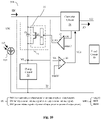
- FIG. 4 shows a schematic block diagram of a power conversion apparatus (i.e., the power conversion apparatus 504 ) for tracking maximum power point according to an embodiment of the present invention.
- a photovoltaic battery 101 which functions as a power retrieval source retrieves photo energy LP and supplies an input power.
- the power conversion apparatus 504 comprises: a signal processing circuit 20 , a comparison circuit 30 , a comparison circuit 35 and a converter circuit 40 .
- the signal processing circuit 20 is coupled to the input power and is configured to operably generate a sensing signal VA at a sensing node NS according to an input voltage VIN of the input power.
- the comparison circuit 30 is configured to operably generate a control signal VCT according to a difference between the sensing signal VA and a reference voltage VREF 1 .
- the converter circuit 40 is configured to operably convert the input power to an output power according to the control signal VCT, so as to supply the output power to a load circuit 50 .
- the comparison circuit 35 is configured to operably sense a sensing signal DS generated by the converter circuit 40 . And, the comparison circuit 35 is configured to operably generate a control signal CPO according to a difference between the sensing signal DS and a reference signal REF 2 .
- the power retrieval source is not limited to a photovoltaic battery 101 ; it is also practicable and within the scope of the present invention that the power retrieval source can be any other type of power retrieval source. That is, the input power can come from any form of power source, not limited to the photo energy LP.
- the converter circuit 40 for example can be a low dropout regulator (LDO).
- the converter circuit 40 for example can be a boost, buck, buck-boost, flyback or inverting switching regulator.
- the load circuit 50 for example can be a rechargeable battery or any other type of application circuit.
- FIG. 16 shows a schematic diagram of a relationship between the sensing signal VA and the input voltage VIN, wherein a relationship between the clamp voltage VCP and the reference voltage VREF 1 is shown.
- the signal processing circuit 20 includes a bias sensing circuit 21 and a clamp circuit 22 .
- the bias sensing circuit 21 is coupled between the input power and the sensing node NS.
- the bias sensing circuit 21 is configured to operably generate the sensing signal VA at the sensing node NS according to the input voltage VIN.
- the clamp circuit 22 is coupled to the sensing node NS.
- the clamp circuit 22 is configured to operably clamp the sensing signal VA, so that the sensing signal VA is not greater than the clamp voltage VCP (for example, FIG. 16 shows that the sensing signal VA is not greater than the clamp voltage VCP).
- the present invention is characterized in that: the comparison circuit 35 senses the sensing signal DS generated by the converter circuit 40 and generates the control signal CPO according to the difference between the sensing signal DS and the reference signal REF 2 , and the control signal CPO generated by the comparison circuit 35 controls the bias sensing circuit 21 .
- FIG. 6 shows an embodiment of the sensing signal DS and an embodiment of the reference signal REF 2 of the present invention.
- the sensing signal DS can be, for example but not limited to, an input voltage related signal DSV (which is related to the input voltage VIN of the input power) and/or an output voltage related signal DSV (which is related to the output voltage VO of the output power).
- the reference signal REF 2 can correspondingly be, for example but not limited to, a reference voltage VREF 2 .
- FIG. 7 shows another embodiment of the sensing signal DS and another embodiment of the reference signal REF 2 of the present invention.
- the sensing signal DS can be, for example but not limited to, an input current related signal DSI (which is related to the input current IIN of the input power) and/or an output current related signal DSI (which is related to the output current IO of the output power).
- the reference signal REF 2 can correspondingly be, for example but not limited to, a reference current IREF.
- FIG. 8 shows yet another embodiment of the sensing signal DS and yet another embodiment of the reference signal REF 2 of the present invention, and shows an embodiment of a power calculation circuit 412 of a converter circuit 40 of the present invention.
- the sensing signal DS can be, for example but not limited to, a power related signal DSP which is related to the input power and/or a power related signal DSP which is related to the output power.
- the reference signal REF 2 can correspondingly be, for example but not limited to, a reference power PREF.
- the converter circuit 40 can include a power calculation circuit 412 .
- the sensing signal DS can include, for example but not limited to, a combination of two or more of the above-mentioned three embodiments.
- the present invention is characterized in that: on one hand, the comparison circuit 30 generates the control signal VCT according to the difference between the sensing signal VA and the reference voltage VREF 1 , whereby the power conversion apparatus 504 can control the converter circuit 40 according to the control signal VCT, to convert the input power to an output power.
- the power conversion apparatus 504 senses the sensing signal DS generated by the converter circuit 40 via the comparison circuit 35 , and the comparison circuit 35 generates the control signal CPO according to the difference between the sensing signal DS and the reference signal REF 2 ; the control signal CPO generated by the comparison circuit 35 controls the bias sensing circuit 21 .
- the power conversion apparatus 504 can further control the bias sensing circuit 21 via the control signal CPO, so that the bias sensing circuit 21 can adjust the sensing signal VA according to the control signal CPO (the features and the details as to how the control signal CPO controls the bias sensing circuit 21 to adjust the sensing signal VA will be described later).
- the power conversion apparatus 504 can adjust the control signal VCT, so that the converter circuit 40 is controlled via an “adjusted” control signal VCT to adjust the output voltage VO and/or the output current IO of the output power, whereby the photovoltaic battery 101 can operate substantially near the maximum power point (MMP).
- MMP maximum power point
- the present invention is characterized and advantageous in that: first, the power conversion apparatus 504 controls the converter circuit 40 via the control signal VCT, wherein the generation of the control signal VCT is in correlation with the sensing signal VA generated by the signal processing circuit 20 . Second, the power conversion apparatus 504 senses the sensing signal DS generated by the converter circuit 40 via the comparison circuit 35 and the comparison circuit 35 generates the control signal CPO according to the sensing signal DS, wherein he generation of the control signal CPO is in correlation with the sensing signal DS. Because the power conversion apparatus 504 can control the bias sensing circuit 21 via the control signal CPO, the bias sensing circuit 21 can adjust the sensing signal VA according to the control signal CPO.
- the comparison circuit 30 of the power conversion apparatus 504 can generate an adjusted control signal VCT according to the difference between the adjusted sensing signal VA and the reference voltage VREF 1 .
- the power conversion apparatus 504 can control the converter circuit 40 via the adjusted control signal VCT to adjust the output voltage VO and/or the output current IO of the output power, so that the photovoltaic battery 101 can operate substantially near the maximum power point (MMP).
- the term “operate substantially near” does require the photovoltaic battery 101 to operate precisely at the maximum power point (MPP); instead, a tolerable error is acceptable.
- control signal CPO controls the bias sensing circuit 21 to adjust the sensing signal VA.
- the bias sensing circuit 21 includes: a sensing capacitor CS and a discharge device 25 .
- the sensing capacitor CS is coupled between the input power and the sensing node NS.
- the sensing capacitor CS and the discharge device 25 are connected in parallel between the input power and the sensing node NS.
- the discharge device 25 is configured to operably control whether the sensing capacitor CS is discharged according to the control signal CPO, so as to adjust a level of the sensing signal VA.
- the present invention is advantageous in that: the present invention can control the bias sensing circuit 21 via the control signal CPO, so as to adjust the sensing signal VA.
- the present invention can control the discharge device 25 of the bias sensing circuit 21 via the control signal CPO; the discharge device 25 controls the sensing capacitor CS of the bias sensing circuit 21 according to the control signal CPO, so as to adjust the level of the sensing signal VA.
- the discharge device 25 can discharge the sensing capacitor CS according to the control signal CPO, so as to raise up the level of the sensing signal VA.
- FIG. 9 shows an embodiment of a discharge device 25 of the present invention.
- the discharge device 25 can be, for example but not limited to, a transistor switch M.
- the control signal CPO can be arranged to control a control terminal of the transistor switch M, to control the conduction of the transistor switch M, thereby controlling whether the sensing capacitor CS is discharged.
- the present invention can control the bias sensing circuit 21 via the control signal CPO, so as to adjust the sensing signal VA.
- the present invention can control the discharge device 25 (the transistor switch M in FIG. 9 ) of the bias sensing circuit 21 via the control signal CPO, to discharge the sensing capacitor CS of the bias sensing circuit 21 according to the control signal CPO, so as to adjust the level of the sensing signal VA.
- the transistor switch M is turned ON according to the control signal CPO to discharge the sensing capacitor CS, so as to raise up the level of the sensing signal VA.
- FIG. 10 shows another embodiment of a discharge device 25 of the present invention.
- the discharge device 25 can include, for example but not limited to, a transistor switch M and a single pulse generation circuit 26 .
- the single pulse generation circuit 26 is coupled between the comparison circuit 35 and the transistor switch M.
- the single pulse generation circuit 26 is configured to operably generate a single pulse signal S 1 according to the control signal CPO.
- the single pulse signal S 1 controls a control terminal of the transistor switch M, to turn ON the transistor switch M for a single pulse period PS (e.g., as shown in FIGS. 13B ′ 14 B and 15 ) corresponding to the single pulse signal S 1 , thereby discharging the sensing capacitor CS.
- PS e.g., as shown in FIGS. 13B ′ 14 B and 15
- the present invention can control the bias sensing circuit 21 via the control signal CPO, so as to adjust the sensing signal VA.
- the present invention can control the discharge device 25 (the transistor switch M and the single pulse generation circuit 26 in FIG. 10 ) of the bias sensing circuit 21 via the control signal CPO, wherein the single pulse generation circuit 26 can control the conduction of the transistor switch M to discharge the sensing capacitor CS of the bias sensing circuit 21 according to the control signal CPO, so as to adjust the level of the sensing signal VA.
- the single pulse generation circuit 26 can generate the single pulse signal S 1 according to the control signal CPO.
- the single pulse signal S 1 turns ON the transistor switch M for the single pulse period PS, to discharge the sensing capacitor CS according to the control signal CPO, so as to raise up the level of the sensing signal VA.
- FIG. 11 shows yet another embodiment of a discharge device 25 of the present invention.
- the discharge device 25 can include, for example but not limited to, a transistor switch M and a resistor RP.
- This embodiment of FIG. 11 is similar to the embodiment of FIG. 9 , but is different in that the embodiment of FIG. 11 further includes a resistor RP.
- the transistor switch M and the resistor RP are connected in parallel between the input power and the sensing node NS.
- the transistor switch M in the embodiment of FIG. 11 operates in the same way as the transistor switch M in the embodiment of FIG. 9 , so the details thereof are not redundantly repeated here, and only the implementation details of the resistor RP are explained below.
- the resistance of the resistor RP and the capacitance of the sensing capacitor CS are so arranged that the sensing capacitor CS can hold the voltage difference (i.e., VIN-VCP) for at least a predetermined holding period (the features and the details of the clamp voltage VCP will be described later).
- the predetermined holding period is related to an operation bandwidth of the power conversion apparatus.
- the resistor RP can be a parasitic resistor of the sensing capacitor CS; in this case, because an actual resistor device is not required, the cost can be reduced.
- the operation point of the photovoltaic battery 101 can be adjusted by selecting or adjusting the resistance of the resistor RP.
- the photovoltaic battery 101 can be adjusted to operate at a relatively low voltage (i.e., a relatively low MPP voltage); by selecting or adjusting the resistance of the resistor RP to be a relatively high resistance, the photovoltaic battery 101 can be adjusted to operate at a relatively high voltage (i.e., a relatively high MPP voltage).
- FIG. 12 shows still another embodiment of a discharge device 25 of the present invention.
- the discharge device 25 can include, for example but not limited to, a transistor switch M, a single pulse generation circuit 26 and a resistor RP.
- This embodiment of FIG. 12 is similar to the embodiment of FIG. 10 , but is different in that: the embodiment of FIG. 12 further includes a resistor RP.
- the transistor switch M single and the single pulse generation circuit 26 in the embodiment of FIG. 12 operate in the same way as the transistor switch M and the single pulse generation circuit 26 in the embodiment of FIG. 10 , so the details thereof are not redundantly repeated here.
- the resistor RP in the embodiment of FIG. 12 operates in the same way as the resistor RP in the embodiment of FIG. 11 , so the details thereof are not redundantly repeated here.
- FIGS. 9 to 12 illustrate exemplary features and details of the discharge device 25 .
- the present invention can control the discharge device 25 of the bias sensing circuit 21 via the control signal CPO, thereby controlling whether the sensing capacitor CS of the bias sensing circuit 21 is discharged, so as to adjust the level of the sensing signal VA.
- Those skilled in this art can readily conceive to modify the discharge device 25 of the above-mentioned four embodiments shown in FIGS. 9 to 12 by a combination of two or more of the above-mentioned embodiments, which should fall within the scope of the present invention.
- the above description explains how the bias sensing circuit 21 of the signal processing circuit 20 functions so that the power conversion apparatus 504 can control the bias sensing circuit 21 via the control signal CPO to adjust the sensing signal VA, and thereby to adjust the control signal VCT, so that the power conversion apparatus 504 can control the converter circuit 40 via the adjusted control signal VCT.
- the comparison circuit 30 is configured to operably generate the control signal VCT according to the difference between the sensing signal VA generated by the signal processing circuit 20 and the reference voltage VREF 1 .
- the power conversion apparatus 504 can control the converter circuit 40 via the control signal VCT, such that the converter circuit 40 can convert the input power to the output power according to the control signal VCT, so as to supply the output power to a load circuit 50 .
- the clamp circuit 22 of the signal processing circuit 20 functions to assist the above mechanism will be explained in the following paragraphs.
- the clamp circuit 22 clamps the sensing signal VA at the clamp voltage VCP, and the sensing capacitor CS samples a voltage difference (i.e., VIN-VCP) between the input voltage VIN and the clamp voltage VCP; when the input voltage VIN decreases below a certain level whereby the clamp circuit 22 does not function, the sensing capacitor CS holds the voltage difference (i.e., VIN-VCP) such that the sensing signal VA is lower than the clamp voltage VCP and the sensing signal VA is positively correlated with the input voltage VIN.
- the sensing capacitor CS can be regarded as high pass filter, by which the sensing signal VA is configured to respond to the high-frequency changes in the input voltage VIN.
- the clamp circuit 22 “functions” or “does not function” should be understood as thus.
- the sensing signal VA generated by the bias sensing circuit 21 according to the input voltage VIN will be greater than the clamp voltage VCP; however, if a clamp circuit 22 is provided as taught by the present invention, the clamp circuit 22 will clamp the sensing signal VA to be at the clamp voltage VCP, so that the sensing signal VA is not greater than the clamp voltage VCP, and this means that the clamp circuit 22 functions.
- the clamp circuit 22 when the sensing signal VA generated by the bias sensing circuit 21 according to the input voltage VIN is lower than the clamp voltage VCP, because the sensing signal VA is lower than the clamp voltage VCP, the clamp circuit 22 does not control the level of the sensing signal VA and this means that the clamp circuit 22 does not function (to clamp the sensing signal VA). From one perspective, when the clamp circuit 22 does not function, the clamp circuit 22 has a high output resistance, and when the clamp circuit 22 functions, the clamp circuit 22 has a low output resistance.
- the converter circuit 40 when the sensing signal VA exceeds the reference voltage VREF 1 , the converter circuit 40 raises up the output voltage VO and/or the output current IO. When the sensing signal VA does not exceed the reference voltage VREF, the converter circuit 40 lowers down the output voltage VO and/or the output current IO. Thus, the photovoltaic battery 101 is controlled to operate substantially near the MPP. According to the present invention, under a dynamic steady state, the sensing signal VA will be at a level which is substantially near the reference voltage VREF 1 by the above-mentioned loop control.
- the clamp voltage VCP can be set to be greater than the reference voltage VREF 1 ; in one preferred embodiment, the clamp voltage VCP is set to be slightly greater than the reference voltage VREF 1 , such that when the input voltage VIN varies (e.g. because of changes in load condition, changes in illumination intensities or changes in temperatures), the power conversion apparatus can respond to the variation within a short time, to control the operation loop such that the photovoltaic battery 101 can rapidly track the updated MPP in response to the changes.
- the reference voltage VREF 1 is not required to be directly correlated to operation parameters of the photovoltaic battery 10 such as the voltage, current or MPP of the photovoltaic battery 10 . That is, as shown in FIG. 16 , in one embodiment, the reference voltage VREF 1 can be any value between the clamp voltage VCP and zero.
- FIG. 3B Please refer to FIG. 3B in in conjugation with FIG. 5 .
- the illumination intensity is very low (e.g., equal to or lower than the value 100 W/m 2 shown in FIG. 3B )
- the MPP voltage of the photovoltaic battery 101 varies greatly in accordance with the changes in the illumination intensities or temperatures.
- the setting of the reference voltage VREF 1 has a great flexibility (i.e., the reference voltage VREF 1 is not required to be directly correlated to operation parameters of the photovoltaic battery 101 such as the voltage, current or MPP of the photovoltaic battery 101 ), and from one perspective, this means that even under a very low illumination intensity, it is not required to adjust the reference voltage VREF 1 in correspondence to different illumination intensities, and via the above-mentioned operation, the power conversion apparatus of the present invention can automatically track the MPP of the photovoltaic battery 101 and operate near the MPP.
- the MPP voltage in normal operation has a trackable range, that is, there is a minimum trackable voltage (VMIN) and there is a maximum trackable voltage (VMAX) for the MPP voltage.
- VMIN minimum trackable voltage
- VMAX maximum trackable voltage
- the minimum trackable voltage VMIN of the power conversion apparatus in correspondence to the same reference voltage VREF 1 , can be equal to or lower than 1 ⁇ 2 of the maximum trackable voltage VMAX. In one preferred embodiment, in correspondence to the same reference voltage VREF 1 , the minimum trackable voltage VMIN of the power conversion apparatus can be equal to or lower than 1 ⁇ 5 of the maximum trackable voltage VMAX.
- the minimum trackable voltage VMIN of the power conversion apparatus can be equal to or lower than 1/10 of the maximum trackable voltage VMAX.
- the MPP voltage of the power conversion apparatus will be greatly decreased as the illumination intensity decreases.
- the power conversion apparatus of the present invention by the same reference voltage VREF 1 , has a very broad range of tractable MPP voltage. As thus, the present invention is advantageous in an environment having low illumination intensity, such as for retrieving indoor illumination energy and converting such indoor illumination energy to electricity.
- FIG. 13A shows a schematic diagram of a relationship between a voltage threshold VTH and a maximum power point voltage where the power conversion apparatus is in normal operation.
- FIG. 13B shows a schematic diagram of signal waveforms of the power conversion apparatus according to an embodiment of the present invention.
- the input voltage VIN or the output voltage VO rises to be higher than the voltage threshold VTH (e.g., as shown by the period from the timing point t 1 to the timing point t 3 in FIG. 13B ) or when the input voltage related signal DSV or the output voltage related signal DSV rises to be higher than the reference voltage VREF 2 (e.g., as shown by the period from the timing point t 1 to the timing point t 3 in FIG.
- the single pulse generation circuit 26 generates the single pulse signal S 1 according to the control signal CPO, so that the transistor switch M is turned ON by the single pulse signal S 1 for the single pulse period PS (e.g., as shown by the period from the timing point t 1 to the timing point t 2 in FIG. 13B ), thereby discharging the sensing capacitor CS; and thus, the level of the control signal VA is raised up.
- the comparison circuit 30 can generate the adjusted control signal VCT according to the difference between the raised sensing signal VA and the reference voltage VREF 1 .
- the power conversion apparatus 510 can control the converter circuit 40 via the adjusted control signal VCT, to raise up the output voltage VO and/or the output current IO of the output power according to the adjusted control signal VCT, so that the photovoltaic battery 101 can operate substantially near the maximum power point (MMP).
- MMP maximum power point
- the voltage threshold VTH can be set to be greater than the MPP voltage where the power conversion apparatus is in normal operation.
- the level of the input voltage related signal DSV can be, for example but not limited to, equal to the level of the input voltage VIN
- the level of the output voltage related signal DSV can be, for example but not limited to, equal to the level of the output voltage VO.
- the level of the input voltage related signal DSV can be, for example but not limited to, positively correlated to the level of the input voltage VIN
- the level of the output voltage related signal DSV can be, for example but not limited to, positively correlated to the level of the output voltage VO.
- the reference voltage VREF 2 is a signal related to the voltage threshold VTH.
- the level of the reference voltage VREF 2 can be, for example but not limited to, equal to the level of the voltage threshold VTH.
- the level of the reference voltage VREF 2 can be, for example but not limited to, positively correlated to the level of the voltage threshold VTH.
- FIG. 14A shows a schematic diagram of a relationship between a current threshold ITH and a maximum power point current where the power conversion apparatus is in normal operation.
- FIG. 14B shows a schematic diagram of signal waveforms of the power conversion apparatus according to an embodiment of the present invention.
- the input current IIN or the output current IO drops to be lower than the current threshold ITH (e.g., as shown by the period from the timing point t 1 to the timing point t 3 in FIG. 14B ) or when the input current related signal DSI or the output current related signal DSI drops to be lower than the reference current IREF (e.g., as shown by the period from the timing point t 1 to the timing point t 3 in FIG.
- the single pulse generation circuit 26 generates the single pulse signal S 1 according to the control signal CPO, so that the transistor switch M is turned ON by the single pulse signal S 1 for the single pulse period PS (e.g., as shown by the period from the timing point t 1 to the timing point t 2 in FIG. 14B ), thereby discharging the sensing capacitor CS; accordingly, the level of the control signal VA is raised up.
- the comparison circuit 30 can generate the adjusted control signal VCT according to the difference between the raised sensing signal VA and the reference voltage VREF 1 .
- the power conversion apparatus 510 can control the converter circuit 40 via the adjusted control signal VCT, to raise up the output voltage VO and/or the output current IO of the output power according to the adjusted control signal VCT, so that the photovoltaic battery 101 can operate substantially near the maximum power point (MMP).
- MMP maximum power point
- the current threshold ITH can be set to be greater than the MPP current where the power conversion apparatus is in normal operation.
- the level of the input current related signal DSI can be, for example but not limited to, equal to the level of the input current IIN
- the level of the output current related signal DSI can be, for example but not limited to, equal to the level of the output current IO.
- the level of the input current related signal DSI can be, for example but not limited to, positively correlated to the level of the input current IIN
- the level of the output current related signal DSI can be, for example but not limited to, positively correlated to the level of the output current IO.
- the reference current IREF is a signal related to the current threshold ITH.
- the level of the reference current IREF can be, for example but not limited to, equal to the level of the current threshold ITH.
- the level of the reference current IREF can be, for example but not limited to, positively correlated to the level of the current threshold ITH.
- FIG. 15 shows a schematic diagram of signal waveforms of the power conversion apparatus according to an embodiment of the present invention.
- the power threshold PTH e.g., as shown by the period from the timing point t 1 to the timing point t 3 in FIG. 15
- the power related signal DSP of the power PIN of the input power or the power related signal DSP of the power PO of the output power drops to be lower than the reference power PREF (e.g., as shown by the period from the timing point t 1 to the timing point t 3 in FIG.
- the single pulse generation circuit 26 generates the single pulse signal S 1 according to the control signal CPO, so that the transistor switch M is turned ON by the single pulse signal S 1 for the single pulse period PS (e.g., as shown by the period from the timing point t 1 to the timing point t 2 in FIG. 15 ), thereby discharging the sensing capacitor CS; accordingly, the level of the control signal VA is raised up.
- the comparison circuit 30 can generate the adjusted control signal VCT according to the difference between the raised sensing signal VA and the reference voltage VREF 1 .
- the power conversion apparatus 510 can control the converter circuit 40 via the adjusted control signal VCT, to raise up the output voltage VO and/or the output current IO of the output power according to the adjusted control signal VCT, so that the photovoltaic battery 101 can operate substantially near the maximum power point (MMP).
- MMP maximum power point
- the level of the power related signal DSP of the power PIN of the input power can be, for example but not limited to, equal to the level of the power PIN of the input power
- the level of the power related signal DSP of the power PO of the output power can be, for example but not limited to, equal to the level of the power PO of the output power.
- the level of the power related signal DSP of the power PIN of the input power can be, for example but not limited to, positively correlated to the level of the power PIN of the input power
- the level of the power related signal DSP of the power PO of the output power can be, for example but not limited to, positively correlated to the level of the power PO of the output power.
- the reference power PREF is a signal related to the power threshold PTH.
- the level of the reference power PREF can be, for example but not limited to, equal to the level of the power threshold PTH.
- the level of the reference power PREF can be, for example but not limited to, positively correlated to the level of the power threshold PTH.
- the power conversion apparatus of the present invention can automatically track the MPP of the photovoltaic battery 101 and operate near the MPP.
- the power conversion apparatus of the present invention can control the bias sensing circuit 21 via the control signal CPO generated by the comparison circuit 35 , to adjust the sensing signal VA, to thereby adjust the control signal VCT generated by the comparison circuit 30 .
- the power conversion apparatus of the present invention can control the converter circuit 40 via an adjusted control signal VCT, such that the converter circuit 40 can adjust the output voltage VO and/or the output current IO of the output power according to the adjusted control signal VCT, so that the photovoltaic battery 101 can operate substantially near the maximum power point (MMP).
- VCT adjusted control signal
- MMP maximum power point
- FIG. 17 shows an embodiment of a clamp circuit 22 of the present invention.
- the clamp circuit 22 for example includes a diode D 1 .
- the clamp voltage VCP is related to the forward bias voltage of the diode D 1 .
- the clamp circuit 22 for example can include plural diodes, such as a diode group consisting of diodes connected in series. Under such situation, the clamp voltage VCP is related to a sum of the forward bias voltages of the diode group.
- FIG. 18 shows another embodiment of the clamp circuit 22 of the present invention.
- the clamp circuit 22 for example can include a Zener diode DZ, wherein the clamp voltage VCP is related to the Zener voltage of the Zener diode DZ.
- the clamp circuit 22 for example can include a transistor (as shown by P 1 in FIG. 19 or as shown by Q 1 in FIG. 20 ) having a control terminal coupled to a bias voltage VB and having a same-phase voltage input end coupled to the sensing node NS.
- the clamp voltage VCP is related to the bias voltage VB and the ON-threshold voltage of the transistor.
- the transistor P 1 can be, for example but not limited to, a PMOS transistor (as shown in FIG. 19 ).
- the transistor Q 1 can be, for example but not limited to, a PNP BJT transistor (as shown in FIG. 20 ).
- the term “same-phase voltage input end” refers to an input end of a transistor which has a same-phase change as the control terminal of the transistor, which is a source of the PMOS transistor P 1 in FIG. 19 , or an emitter of the PNP BJT transistor Q 1 in FIG. 20 .
- FIG. 21 shows another embodiment of a signal processing circuit of the present invention (i.e., signal processing circuit 20 ′).
- the signal processing circuit 20 ′ further includes an offset device 24 .
- the offset device 24 and the bias sensing circuit 21 are connected in series between the input power and the sensing node NS.
- the offset device 24 is configured to operably provide an offset voltage, so as to generate the sensing signal VA.
- the location of offset device 24 with respect to the bias sensing circuit 21 is not limited to be as shown in the figure.
- the location of the offset device 24 and the location of the bias sensing circuit 21 can be interchanged, that is, the offset device 24 can be directly coupled to the input voltage VIN.
- the offset device 24 includes an offset diode DOS.
- the offset voltage is related to the forward bias voltage of the offset diode DOS.
- the MPP of the photovoltaic battery 101 varies in accordance with changes in temperatures.
- the photovoltaic battery 101 (or any other type of power retrieval source) and the clamp circuit 22 include semiconductor junctions of the same characteristics, such that the variation of the clamp voltage VCP and the variation of the input voltage VIN with respect to a temperature change are positively correlated to each other.
- both of the photovoltaic battery 101 and the clamp circuit 22 e.g., diode D 1
- both of the photovoltaic battery 101 and the clamp circuit 22 include a P-N semiconductor junction, so that the variations of the clamp voltage VCP and the input voltage VIN with respect to a temperature change are positively correlated to each other.
- the clamp device can be a combination of two or more of the above-mentioned diode, Zener diode and transistor. Under such circumstance, the clamp voltage will be a sum of parameters of the respective devices (forward bias voltage, Zener voltage and/or ON-threshold voltage).
- a certain signal as described in the context of the present invention is not limited to performing an action strictly according to the signal itself, but can be performing an action according to a converted form or a scaled-up or down form of the signal, i.e., the signal can be processed by a voltage-to-current conversion, a current-to-voltage conversion, and/or a ratio conversion, etc. before an action is performed. It is not limited for each of the embodiments described herein before to be used alone; under the spirit of the present invention, two or more of the embodiments described hereinbefore can be used in combination.
Landscapes
- Engineering & Computer Science (AREA)
- Power Engineering (AREA)
- Life Sciences & Earth Sciences (AREA)
- Sustainable Development (AREA)
- Sustainable Energy (AREA)
- Physics & Mathematics (AREA)
- Electromagnetism (AREA)
- General Physics & Mathematics (AREA)
- Radar, Positioning & Navigation (AREA)
- Automation & Control Theory (AREA)
- Dc-Dc Converters (AREA)
- Control Of Electrical Variables (AREA)
Priority Applications (1)
| Application Number | Priority Date | Filing Date | Title |
|---|---|---|---|
| US16/730,940 US11340645B2 (en) | 2019-03-06 | 2019-12-30 | Power conversion apparatus for tracking maximum power point and control method thereof |
Applications Claiming Priority (4)
| Application Number | Priority Date | Filing Date | Title |
|---|---|---|---|
| US201962814720P | 2019-03-06 | 2019-03-06 | |
| TW108125970A TWI695249B (zh) | 2019-03-06 | 2019-07-23 | 可追蹤最大功率點的電源轉換裝置及其中之控制方法 |
| TW108125970 | 2019-07-23 | ||
| US16/730,940 US11340645B2 (en) | 2019-03-06 | 2019-12-30 | Power conversion apparatus for tracking maximum power point and control method thereof |
Publications (2)
| Publication Number | Publication Date |
|---|---|
| US20200285263A1 US20200285263A1 (en) | 2020-09-10 |
| US11340645B2 true US11340645B2 (en) | 2022-05-24 |
Family
ID=72176086
Family Applications (1)
| Application Number | Title | Priority Date | Filing Date |
|---|---|---|---|
| US16/730,940 Active 2040-10-20 US11340645B2 (en) | 2019-03-06 | 2019-12-30 | Power conversion apparatus for tracking maximum power point and control method thereof |
Country Status (3)
| Country | Link |
|---|---|
| US (1) | US11340645B2 (zh) |
| CN (1) | CN111669051B (zh) |
| TW (1) | TWI695249B (zh) |
Citations (3)
| Publication number | Priority date | Publication date | Assignee | Title |
|---|---|---|---|---|
| US3566143A (en) * | 1969-03-11 | 1971-02-23 | Nasa | Maximum power point tracker |
| US4272806A (en) * | 1979-06-08 | 1981-06-09 | Eastman Kodak Company | DC to DC Converter adjustable dynamically to battery condition |
| US4390940A (en) * | 1980-06-26 | 1983-06-28 | Societe Nationale Industrielle Aerospatiale | Process and system for producing photovoltaic power |
Family Cites Families (17)
| Publication number | Priority date | Publication date | Assignee | Title |
|---|---|---|---|---|
| US4604567A (en) * | 1983-10-11 | 1986-08-05 | Sundstrand Corporation | Maximum power transfer system for a solar cell array |
| DE3725476A1 (de) * | 1987-07-31 | 1989-02-09 | Siemens Ag | Schaltungsanordnung zur speisung einer elektrischen last aus einer elektrischen energiequelle mit schwankender leistungsfaehigkeit |
| FR2844890B1 (fr) * | 2002-09-19 | 2005-01-14 | Cit Alcatel | Circuit de conditionnement pour une source de puissance au point de puissance maximum, generateur solaire et procede de conditionnement |
| CN101211192B (zh) * | 2006-12-31 | 2011-08-24 | 立锜科技股份有限公司 | 模拟光能电路 |
| CN101694942B (zh) * | 2009-10-16 | 2011-03-02 | 山东电力研究院 | 最大功率追踪方法 |
| US8922185B2 (en) * | 2011-07-11 | 2014-12-30 | Solarbridge Technologies, Inc. | Device and method for global maximum power point tracking |
| WO2014062167A1 (en) * | 2012-10-16 | 2014-04-24 | Volterra Semiconductor Corporation | Maximum power point tracking controllers and associated systems and methods |
| CN102880224A (zh) * | 2012-10-26 | 2013-01-16 | 天津理工大学 | 基于改进步长的双模式最大功率点跟踪方法 |
| US9804627B2 (en) * | 2013-12-06 | 2017-10-31 | Sparq Systems Inc. | Multi-input PV inverter with independent MPPT and minimum energy storage |
| TWI553440B (zh) * | 2015-02-26 | 2016-10-11 | 國立中山大學 | 太陽光伏發電之最大功率追蹤方法 |
| TW201643589A (zh) * | 2015-06-02 | 2016-12-16 | 群光電能科技股份有限公司 | 最大功率追蹤電路及發電系統及最大功率追蹤方法 |
| MY194129A (en) * | 2015-11-19 | 2022-11-14 | Sigmagen Inc | Multi-modal maximum power point tracking optimzation solar photovoltaic system |
| JP6894219B2 (ja) * | 2016-11-28 | 2021-06-30 | トヨタ自動車株式会社 | 太陽光発電制御装置 |
| JP6799502B2 (ja) * | 2017-06-06 | 2020-12-16 | 株式会社日立インダストリアルプロダクツ | 太陽光発電用電力変換装置および太陽光発電用電力変換装置の制御方法 |
| CN109144162A (zh) * | 2018-08-03 | 2019-01-04 | 东泰高科装备科技有限公司 | 光伏电池的最大功率点跟踪方法及装置、存储介质 |
| CN108983864B (zh) * | 2018-10-15 | 2020-06-30 | 西安许继电力电子技术有限公司 | 一种光伏最大功率点的跟踪方法及其跟踪装置 |
| CN109270982A (zh) * | 2018-11-20 | 2019-01-25 | 西安科技大学 | 一种太阳能光伏最大功率跟踪控制方法 |
-
2019
- 2019-07-23 TW TW108125970A patent/TWI695249B/zh active
- 2019-08-02 CN CN201910711228.4A patent/CN111669051B/zh active Active
- 2019-12-30 US US16/730,940 patent/US11340645B2/en active Active
Patent Citations (3)
| Publication number | Priority date | Publication date | Assignee | Title |
|---|---|---|---|---|
| US3566143A (en) * | 1969-03-11 | 1971-02-23 | Nasa | Maximum power point tracker |
| US4272806A (en) * | 1979-06-08 | 1981-06-09 | Eastman Kodak Company | DC to DC Converter adjustable dynamically to battery condition |
| US4390940A (en) * | 1980-06-26 | 1983-06-28 | Societe Nationale Industrielle Aerospatiale | Process and system for producing photovoltaic power |
Also Published As
| Publication number | Publication date |
|---|---|
| CN111669051B (zh) | 2021-07-23 |
| CN111669051A (zh) | 2020-09-15 |
| US20200285263A1 (en) | 2020-09-10 |
| TW202034111A (zh) | 2020-09-16 |
| TWI695249B (zh) | 2020-06-01 |
Similar Documents
| Publication | Publication Date | Title |
|---|---|---|
| US10581332B2 (en) | Dimmer and power converter | |
| US9081401B2 (en) | Switching regulator and control circuit and control method thereof | |
| US8018741B2 (en) | Adjusting for conductor loss to regulate constant output voltage in a primary feedback converter | |
| US7071630B1 (en) | Closed loop magnetic boost LED driver system and method | |
| US7307390B2 (en) | Primary side constant output voltage controller | |
| TWI441427B (zh) | 並聯調節器、返馳轉換器及其輸出回授的控制方法 | |
| US20080149167A1 (en) | Analog photovoltaic power circuit | |
| US20190146532A1 (en) | Feedback circuit for regulation loops | |
| US20110025283A1 (en) | Dc-dc converter, control circuit, and power supply control method | |
| US8300381B2 (en) | Low cost high speed spark voltage and flame drive signal generator | |
| US20140285109A1 (en) | Light emitting device driver circuit and control circuit and control method thereof | |
| US20130088169A1 (en) | Constant-current led driver circuit and output voltage adjustable circuit and method thereof | |
| US9167648B2 (en) | Lighting device and luminaire | |
| US10536082B2 (en) | Power supply device, semiconductor integrated circuit, and method for suppressing ripple component | |
| KR20110046926A (ko) | 역률 보상 회로 및 역률보상 회로의 구동 방법 | |
| CN115378413B (zh) | 控制电路及控制方法 | |
| US20160344212A1 (en) | Power generation system of renewable-energy-based electric power generator and dc power source combiner provided with reverse current prevention device capable of preventing power loss in power generation system | |
| WO2006046731A1 (ja) | 電源装置、および携帯機器 | |
| US10642301B2 (en) | Power conversion apparatus for tracking maximum power point and control method thereof | |
| US11340645B2 (en) | Power conversion apparatus for tracking maximum power point and control method thereof | |
| US8853994B2 (en) | Analog photovoltaic power circuit | |
| CN110377098B (zh) | 可追踪最大功率点的电源转换装置及其中的控制方法 | |
| US20190386556A1 (en) | Multi-source energy harvester system and power conversion apparatus and method thereof | |
| US11139670B2 (en) | Charger circuit with temperature compensation function and controller circuit thereof | |
| US20220329154A1 (en) | Switch mode power supply with improved transient performance and control circuit thereof |
Legal Events
| Date | Code | Title | Description |
|---|---|---|---|
| AS | Assignment |
Owner name: RICHTEK TECHNOLOGY CORPORATION, TAIWAN Free format text: ASSIGNMENT OF ASSIGNORS INTEREST;ASSIGNOR:LIU, KUO-CHI;REEL/FRAME:051390/0124 Effective date: 20190717 |
|
| FEPP | Fee payment procedure |
Free format text: ENTITY STATUS SET TO UNDISCOUNTED (ORIGINAL EVENT CODE: BIG.); ENTITY STATUS OF PATENT OWNER: LARGE ENTITY |
|
| STPP | Information on status: patent application and granting procedure in general |
Free format text: DOCKETED NEW CASE - READY FOR EXAMINATION |
|
| STPP | Information on status: patent application and granting procedure in general |
Free format text: EX PARTE QUAYLE ACTION MAILED |
|
| STPP | Information on status: patent application and granting procedure in general |
Free format text: RESPONSE TO EX PARTE QUAYLE ACTION ENTERED AND FORWARDED TO EXAMINER |
|
| STPP | Information on status: patent application and granting procedure in general |
Free format text: NOTICE OF ALLOWANCE MAILED -- APPLICATION RECEIVED IN OFFICE OF PUBLICATIONS |
|
| STPP | Information on status: patent application and granting procedure in general |
Free format text: PUBLICATIONS -- ISSUE FEE PAYMENT VERIFIED |
|
| STCF | Information on status: patent grant |
Free format text: PATENTED CASE |