US11233144B2 - Nitride semiconductor device and nitride semiconductor package - Google Patents
Nitride semiconductor device and nitride semiconductor package Download PDFInfo
- Publication number
- US11233144B2 US11233144B2 US16/405,417 US201916405417A US11233144B2 US 11233144 B2 US11233144 B2 US 11233144B2 US 201916405417 A US201916405417 A US 201916405417A US 11233144 B2 US11233144 B2 US 11233144B2
- Authority
- US
- United States
- Prior art keywords
- layer
- nitride semiconductor
- gate
- electron
- electron supply
- Prior art date
- Legal status (The legal status is an assumption and is not a legal conclusion. Google has not performed a legal analysis and makes no representation as to the accuracy of the status listed.)
- Active, expires
Links
Images


Classifications
-
- H01L29/7787—
-
- H—ELECTRICITY
- H10—SEMICONDUCTOR DEVICES; ELECTRIC SOLID-STATE DEVICES NOT OTHERWISE PROVIDED FOR
- H10D—INORGANIC ELECTRIC SEMICONDUCTOR DEVICES
- H10D30/00—Field-effect transistors [FET]
- H10D30/40—FETs having zero-dimensional [0D], one-dimensional [1D] or two-dimensional [2D] charge carrier gas channels
- H10D30/47—FETs having zero-dimensional [0D], one-dimensional [1D] or two-dimensional [2D] charge carrier gas channels having 2D charge carrier gas channels, e.g. nanoribbon FETs or high electron mobility transistors [HEMT]
- H10D30/471—High electron mobility transistors [HEMT] or high hole mobility transistors [HHMT]
- H10D30/475—High electron mobility transistors [HEMT] or high hole mobility transistors [HHMT] having wider bandgap layer formed on top of lower bandgap active layer, e.g. undoped barrier HEMTs such as i-AlGaN/GaN HEMTs
- H10D30/4755—High electron mobility transistors [HEMT] or high hole mobility transistors [HHMT] having wider bandgap layer formed on top of lower bandgap active layer, e.g. undoped barrier HEMTs such as i-AlGaN/GaN HEMTs having wide bandgap charge-carrier supplying layers, e.g. modulation doped HEMTs such as n-AlGaAs/GaAs HEMTs
-
- H—ELECTRICITY
- H01—ELECTRIC ELEMENTS
- H01L—SEMICONDUCTOR DEVICES NOT COVERED BY CLASS H10
- H01L23/00—Details of semiconductor or other solid state devices
- H01L23/28—Encapsulations, e.g. encapsulating layers, coatings, e.g. for protection
- H01L23/31—Encapsulations, e.g. encapsulating layers, coatings, e.g. for protection characterised by the arrangement or shape
- H01L23/3107—Encapsulations, e.g. encapsulating layers, coatings, e.g. for protection characterised by the arrangement or shape the device being completely enclosed
- H01L23/3114—Encapsulations, e.g. encapsulating layers, coatings, e.g. for protection characterised by the arrangement or shape the device being completely enclosed the device being a chip scale package, e.g. CSP
-
- H—ELECTRICITY
- H01—ELECTRIC ELEMENTS
- H01L—SEMICONDUCTOR DEVICES NOT COVERED BY CLASS H10
- H01L23/00—Details of semiconductor or other solid state devices
- H01L23/48—Arrangements for conducting electric current to or from the solid state body in operation, e.g. leads, terminal arrangements ; Selection of materials therefor
- H01L23/488—Arrangements for conducting electric current to or from the solid state body in operation, e.g. leads, terminal arrangements ; Selection of materials therefor consisting of soldered or bonded constructions
- H01L23/495—Lead-frames or other flat leads
- H01L23/49541—Geometry of the lead-frame
- H01L23/49562—Geometry of the lead-frame for individual devices of subclass H10D
-
- H01L29/2003—
-
- H01L29/205—
-
- H01L29/475—
-
- H01L29/66462—
-
- H01L29/7786—
-
- H—ELECTRICITY
- H10—SEMICONDUCTOR DEVICES; ELECTRIC SOLID-STATE DEVICES NOT OTHERWISE PROVIDED FOR
- H10D—INORGANIC ELECTRIC SEMICONDUCTOR DEVICES
- H10D30/00—Field-effect transistors [FET]
- H10D30/01—Manufacture or treatment
- H10D30/015—Manufacture or treatment of FETs having heterojunction interface channels or heterojunction gate electrodes, e.g. HEMT
-
- H—ELECTRICITY
- H10—SEMICONDUCTOR DEVICES; ELECTRIC SOLID-STATE DEVICES NOT OTHERWISE PROVIDED FOR
- H10D—INORGANIC ELECTRIC SEMICONDUCTOR DEVICES
- H10D30/00—Field-effect transistors [FET]
- H10D30/40—FETs having zero-dimensional [0D], one-dimensional [1D] or two-dimensional [2D] charge carrier gas channels
- H10D30/47—FETs having zero-dimensional [0D], one-dimensional [1D] or two-dimensional [2D] charge carrier gas channels having 2D charge carrier gas channels, e.g. nanoribbon FETs or high electron mobility transistors [HEMT]
- H10D30/471—High electron mobility transistors [HEMT] or high hole mobility transistors [HHMT]
- H10D30/475—High electron mobility transistors [HEMT] or high hole mobility transistors [HHMT] having wider bandgap layer formed on top of lower bandgap active layer, e.g. undoped barrier HEMTs such as i-AlGaN/GaN HEMTs
-
- H—ELECTRICITY
- H10—SEMICONDUCTOR DEVICES; ELECTRIC SOLID-STATE DEVICES NOT OTHERWISE PROVIDED FOR
- H10D—INORGANIC ELECTRIC SEMICONDUCTOR DEVICES
- H10D30/00—Field-effect transistors [FET]
- H10D30/60—Insulated-gate field-effect transistors [IGFET]
- H10D30/67—Thin-film transistors [TFT]
- H10D30/6729—Thin-film transistors [TFT] characterised by the electrodes
- H10D30/6737—Thin-film transistors [TFT] characterised by the electrodes characterised by the electrode materials
- H10D30/6738—Schottky barrier electrodes
-
- H—ELECTRICITY
- H10—SEMICONDUCTOR DEVICES; ELECTRIC SOLID-STATE DEVICES NOT OTHERWISE PROVIDED FOR
- H10D—INORGANIC ELECTRIC SEMICONDUCTOR DEVICES
- H10D30/00—Field-effect transistors [FET]
- H10D30/60—Insulated-gate field-effect transistors [IGFET]
- H10D30/67—Thin-film transistors [TFT]
- H10D30/674—Thin-film transistors [TFT] characterised by the active materials
- H10D30/675—Group III-V materials, Group II-VI materials, Group IV-VI materials, selenium or tellurium
-
- H—ELECTRICITY
- H10—SEMICONDUCTOR DEVICES; ELECTRIC SOLID-STATE DEVICES NOT OTHERWISE PROVIDED FOR
- H10D—INORGANIC ELECTRIC SEMICONDUCTOR DEVICES
- H10D62/00—Semiconductor bodies, or regions thereof, of devices having potential barriers
- H10D62/80—Semiconductor bodies, or regions thereof, of devices having potential barriers characterised by the materials
- H10D62/82—Heterojunctions
- H10D62/824—Heterojunctions comprising only Group III-V materials heterojunctions, e.g. GaN/AlGaN heterojunctions
-
- H—ELECTRICITY
- H10—SEMICONDUCTOR DEVICES; ELECTRIC SOLID-STATE DEVICES NOT OTHERWISE PROVIDED FOR
- H10D—INORGANIC ELECTRIC SEMICONDUCTOR DEVICES
- H10D62/00—Semiconductor bodies, or regions thereof, of devices having potential barriers
- H10D62/80—Semiconductor bodies, or regions thereof, of devices having potential barriers characterised by the materials
- H10D62/85—Semiconductor bodies, or regions thereof, of devices having potential barriers characterised by the materials being Group III-V materials, e.g. GaAs
- H10D62/8503—Nitride Group III-V materials, e.g. AlN or GaN
-
- H—ELECTRICITY
- H10—SEMICONDUCTOR DEVICES; ELECTRIC SOLID-STATE DEVICES NOT OTHERWISE PROVIDED FOR
- H10D—INORGANIC ELECTRIC SEMICONDUCTOR DEVICES
- H10D64/00—Electrodes of devices having potential barriers
- H10D64/60—Electrodes characterised by their materials
- H10D64/64—Electrodes comprising a Schottky barrier to a semiconductor
-
- H10W70/481—
-
- H10W74/129—
-
- H—ELECTRICITY
- H01—ELECTRIC ELEMENTS
- H01L—SEMICONDUCTOR DEVICES NOT COVERED BY CLASS H10
- H01L2224/00—Indexing scheme for arrangements for connecting or disconnecting semiconductor or solid-state bodies and methods related thereto as covered by H01L24/00
- H01L2224/01—Means for bonding being attached to, or being formed on, the surface to be connected, e.g. chip-to-package, die-attach, "first-level" interconnects; Manufacturing methods related thereto
- H01L2224/26—Layer connectors, e.g. plate connectors, solder or adhesive layers; Manufacturing methods related thereto
- H01L2224/31—Structure, shape, material or disposition of the layer connectors after the connecting process
- H01L2224/32—Structure, shape, material or disposition of the layer connectors after the connecting process of an individual layer connector
- H01L2224/321—Disposition
- H01L2224/32151—Disposition the layer connector connecting between a semiconductor or solid-state body and an item not being a semiconductor or solid-state body, e.g. chip-to-substrate, chip-to-passive
- H01L2224/32221—Disposition the layer connector connecting between a semiconductor or solid-state body and an item not being a semiconductor or solid-state body, e.g. chip-to-substrate, chip-to-passive the body and the item being stacked
- H01L2224/32245—Disposition the layer connector connecting between a semiconductor or solid-state body and an item not being a semiconductor or solid-state body, e.g. chip-to-substrate, chip-to-passive the body and the item being stacked the item being metallic
-
- H—ELECTRICITY
- H01—ELECTRIC ELEMENTS
- H01L—SEMICONDUCTOR DEVICES NOT COVERED BY CLASS H10
- H01L2224/00—Indexing scheme for arrangements for connecting or disconnecting semiconductor or solid-state bodies and methods related thereto as covered by H01L24/00
- H01L2224/01—Means for bonding being attached to, or being formed on, the surface to be connected, e.g. chip-to-package, die-attach, "first-level" interconnects; Manufacturing methods related thereto
- H01L2224/42—Wire connectors; Manufacturing methods related thereto
- H01L2224/47—Structure, shape, material or disposition of the wire connectors after the connecting process
- H01L2224/48—Structure, shape, material or disposition of the wire connectors after the connecting process of an individual wire connector
- H01L2224/4805—Shape
- H01L2224/4809—Loop shape
- H01L2224/48091—Arched
-
- H—ELECTRICITY
- H01—ELECTRIC ELEMENTS
- H01L—SEMICONDUCTOR DEVICES NOT COVERED BY CLASS H10
- H01L2224/00—Indexing scheme for arrangements for connecting or disconnecting semiconductor or solid-state bodies and methods related thereto as covered by H01L24/00
- H01L2224/01—Means for bonding being attached to, or being formed on, the surface to be connected, e.g. chip-to-package, die-attach, "first-level" interconnects; Manufacturing methods related thereto
- H01L2224/42—Wire connectors; Manufacturing methods related thereto
- H01L2224/47—Structure, shape, material or disposition of the wire connectors after the connecting process
- H01L2224/48—Structure, shape, material or disposition of the wire connectors after the connecting process of an individual wire connector
- H01L2224/481—Disposition
- H01L2224/48151—Connecting between a semiconductor or solid-state body and an item not being a semiconductor or solid-state body, e.g. chip-to-substrate, chip-to-passive
- H01L2224/48221—Connecting between a semiconductor or solid-state body and an item not being a semiconductor or solid-state body, e.g. chip-to-substrate, chip-to-passive the body and the item being stacked
- H01L2224/48245—Connecting between a semiconductor or solid-state body and an item not being a semiconductor or solid-state body, e.g. chip-to-substrate, chip-to-passive the body and the item being stacked the item being metallic
- H01L2224/48247—Connecting between a semiconductor or solid-state body and an item not being a semiconductor or solid-state body, e.g. chip-to-substrate, chip-to-passive the body and the item being stacked the item being metallic connecting the wire to a bond pad of the item
-
- H—ELECTRICITY
- H01—ELECTRIC ELEMENTS
- H01L—SEMICONDUCTOR DEVICES NOT COVERED BY CLASS H10
- H01L2224/00—Indexing scheme for arrangements for connecting or disconnecting semiconductor or solid-state bodies and methods related thereto as covered by H01L24/00
- H01L2224/01—Means for bonding being attached to, or being formed on, the surface to be connected, e.g. chip-to-package, die-attach, "first-level" interconnects; Manufacturing methods related thereto
- H01L2224/42—Wire connectors; Manufacturing methods related thereto
- H01L2224/47—Structure, shape, material or disposition of the wire connectors after the connecting process
- H01L2224/48—Structure, shape, material or disposition of the wire connectors after the connecting process of an individual wire connector
- H01L2224/481—Disposition
- H01L2224/48151—Connecting between a semiconductor or solid-state body and an item not being a semiconductor or solid-state body, e.g. chip-to-substrate, chip-to-passive
- H01L2224/48221—Connecting between a semiconductor or solid-state body and an item not being a semiconductor or solid-state body, e.g. chip-to-substrate, chip-to-passive the body and the item being stacked
- H01L2224/48245—Connecting between a semiconductor or solid-state body and an item not being a semiconductor or solid-state body, e.g. chip-to-substrate, chip-to-passive the body and the item being stacked the item being metallic
- H01L2224/48257—Connecting between a semiconductor or solid-state body and an item not being a semiconductor or solid-state body, e.g. chip-to-substrate, chip-to-passive the body and the item being stacked the item being metallic connecting the wire to a die pad of the item
-
- H—ELECTRICITY
- H01—ELECTRIC ELEMENTS
- H01L—SEMICONDUCTOR DEVICES NOT COVERED BY CLASS H10
- H01L2224/00—Indexing scheme for arrangements for connecting or disconnecting semiconductor or solid-state bodies and methods related thereto as covered by H01L24/00
- H01L2224/01—Means for bonding being attached to, or being formed on, the surface to be connected, e.g. chip-to-package, die-attach, "first-level" interconnects; Manufacturing methods related thereto
- H01L2224/42—Wire connectors; Manufacturing methods related thereto
- H01L2224/47—Structure, shape, material or disposition of the wire connectors after the connecting process
- H01L2224/49—Structure, shape, material or disposition of the wire connectors after the connecting process of a plurality of wire connectors
- H01L2224/491—Disposition
- H01L2224/49105—Connecting at different heights
- H01L2224/49107—Connecting at different heights on the semiconductor or solid-state body
-
- H—ELECTRICITY
- H01—ELECTRIC ELEMENTS
- H01L—SEMICONDUCTOR DEVICES NOT COVERED BY CLASS H10
- H01L2224/00—Indexing scheme for arrangements for connecting or disconnecting semiconductor or solid-state bodies and methods related thereto as covered by H01L24/00
- H01L2224/73—Means for bonding being of different types provided for in two or more of groups H01L2224/10, H01L2224/18, H01L2224/26, H01L2224/34, H01L2224/42, H01L2224/50, H01L2224/63, H01L2224/71
- H01L2224/732—Location after the connecting process
- H01L2224/73251—Location after the connecting process on different surfaces
- H01L2224/73265—Layer and wire connectors
-
- H01L29/1066—
-
- H01L29/402—
-
- H01L29/41766—
-
- H01L29/432—
-
- H01L29/452—
-
- H01L29/4966—
-
- H—ELECTRICITY
- H01—ELECTRIC ELEMENTS
- H01L—SEMICONDUCTOR DEVICES NOT COVERED BY CLASS H10
- H01L2924/00—Indexing scheme for arrangements or methods for connecting or disconnecting semiconductor or solid-state bodies as covered by H01L24/00
-
- H—ELECTRICITY
- H01—ELECTRIC ELEMENTS
- H01L—SEMICONDUCTOR DEVICES NOT COVERED BY CLASS H10
- H01L2924/00—Indexing scheme for arrangements or methods for connecting or disconnecting semiconductor or solid-state bodies as covered by H01L24/00
- H01L2924/0001—Technical content checked by a classifier
- H01L2924/00012—Relevant to the scope of the group, the symbol of which is combined with the symbol of this group
-
- H—ELECTRICITY
- H01—ELECTRIC ELEMENTS
- H01L—SEMICONDUCTOR DEVICES NOT COVERED BY CLASS H10
- H01L2924/00—Indexing scheme for arrangements or methods for connecting or disconnecting semiconductor or solid-state bodies as covered by H01L24/00
- H01L2924/0001—Technical content checked by a classifier
- H01L2924/00014—Technical content checked by a classifier the subject-matter covered by the group, the symbol of which is combined with the symbol of this group, being disclosed without further technical details
-
- H—ELECTRICITY
- H01—ELECTRIC ELEMENTS
- H01L—SEMICONDUCTOR DEVICES NOT COVERED BY CLASS H10
- H01L2924/00—Indexing scheme for arrangements or methods for connecting or disconnecting semiconductor or solid-state bodies as covered by H01L24/00
- H01L2924/15—Details of package parts other than the semiconductor or other solid state devices to be connected
- H01L2924/181—Encapsulation
-
- H—ELECTRICITY
- H10—SEMICONDUCTOR DEVICES; ELECTRIC SOLID-STATE DEVICES NOT OTHERWISE PROVIDED FOR
- H10D—INORGANIC ELECTRIC SEMICONDUCTOR DEVICES
- H10D62/00—Semiconductor bodies, or regions thereof, of devices having potential barriers
- H10D62/10—Shapes, relative sizes or dispositions of the regions of the semiconductor bodies; Shapes of the semiconductor bodies
- H10D62/17—Semiconductor regions connected to electrodes not carrying current to be rectified, amplified or switched, e.g. channel regions
- H10D62/343—Gate regions of field-effect devices having PN junction gates
-
- H—ELECTRICITY
- H10—SEMICONDUCTOR DEVICES; ELECTRIC SOLID-STATE DEVICES NOT OTHERWISE PROVIDED FOR
- H10D—INORGANIC ELECTRIC SEMICONDUCTOR DEVICES
- H10D64/00—Electrodes of devices having potential barriers
- H10D64/111—Field plates
-
- H—ELECTRICITY
- H10—SEMICONDUCTOR DEVICES; ELECTRIC SOLID-STATE DEVICES NOT OTHERWISE PROVIDED FOR
- H10D—INORGANIC ELECTRIC SEMICONDUCTOR DEVICES
- H10D64/00—Electrodes of devices having potential barriers
- H10D64/20—Electrodes characterised by their shapes, relative sizes or dispositions
- H10D64/23—Electrodes carrying the current to be rectified, amplified, oscillated or switched, e.g. sources, drains, anodes or cathodes
- H10D64/251—Source or drain electrodes for field-effect devices
- H10D64/256—Source or drain electrodes for field-effect devices for lateral devices wherein the source or drain electrodes are recessed in semiconductor bodies
-
- H—ELECTRICITY
- H10—SEMICONDUCTOR DEVICES; ELECTRIC SOLID-STATE DEVICES NOT OTHERWISE PROVIDED FOR
- H10D—INORGANIC ELECTRIC SEMICONDUCTOR DEVICES
- H10D64/00—Electrodes of devices having potential barriers
- H10D64/60—Electrodes characterised by their materials
- H10D64/602—Heterojunction gate electrodes for FETs
-
- H—ELECTRICITY
- H10—SEMICONDUCTOR DEVICES; ELECTRIC SOLID-STATE DEVICES NOT OTHERWISE PROVIDED FOR
- H10D—INORGANIC ELECTRIC SEMICONDUCTOR DEVICES
- H10D64/00—Electrodes of devices having potential barriers
- H10D64/60—Electrodes characterised by their materials
- H10D64/62—Electrodes ohmically coupled to a semiconductor
-
- H—ELECTRICITY
- H10—SEMICONDUCTOR DEVICES; ELECTRIC SOLID-STATE DEVICES NOT OTHERWISE PROVIDED FOR
- H10D—INORGANIC ELECTRIC SEMICONDUCTOR DEVICES
- H10D64/00—Electrodes of devices having potential barriers
- H10D64/60—Electrodes characterised by their materials
- H10D64/66—Electrodes having a conductor capacitively coupled to a semiconductor by an insulator, e.g. MIS electrodes
- H10D64/667—Electrodes having a conductor capacitively coupled to a semiconductor by an insulator, e.g. MIS electrodes the conductor comprising a layer of alloy material, compound material or organic material contacting the insulator, e.g. TiN workfunction layers
-
- H10W72/07554—
-
- H10W72/547—
-
- H10W72/884—
-
- H10W74/00—
-
- H10W90/736—
-
- H10W90/756—
Definitions
- the present invention relates to a nitride semiconductor device, having an HEMT (High Electron Mobility Transistor) structure, and a package thereof.
- HEMT High Electron Mobility Transistor
- Japanese Patent Publication No. 4705412 discloses a field effect transistor including a sapphire substrate, an AlN butter layer on the sapphire substrate, an undoped GaN layer on the AlN buffer layer, an undoped AlGaN layer on the undoped GaN layer, a p type GaN layer provided on a portion of the undoped AlGaN layer, a high concentration p type GaN layer on the p type GaN layer, and a gate electrode on the high concentration p type GaN layer.
- the transistor of Patent Document 1 is of the normally-off type
- the layers below the gate electrode contain a p type impurity and therefore whereas holes are implanted from the p type GaN gate layer when the transistor is on, a time corresponding to the carrier life is required when turning off the transistor because the implanted holes must be annihilated by recombination with the electrons, thus making the turnoff time long and making the transistor unsuitable for high speed switching operations.
- An object of the present invention is to provide a normally-off type nitride semiconductor device and a package thereof, with which high speed switching can be achieved.
- the AlGaN layer electron supply layer
- a decrease in gate threshold voltage occurs and in some cases, the transistor becomes normally on. That is, the sheet carrier density outside a gate region directly below the gate electrode and the gate threshold voltage are in a tradeoff relationship.
- An object of the present invention is to provide a nitride semiconductor device and a package thereof, with which both high sheet carrier density and high gate threshold voltage can be realized at the same time.
- a nitride semiconductor device includes an electron transit layer, an electron supply layer, in contact with the electron transit layer and constituted of a nitride semiconductor composition differing from that of the electron transit layer, a gate layer, formed selectively on the electron supply layer and constituted of a nitride semiconductor composition effectively not containing an acceptor type impurity, and a gate electrode, formed on the gate layer, and satisfies the following formula (1):
- the electron transit layer and the gate layer may contain GaN and the electron supply layer may contain AlGaN.
- the effective acceptor concentration N DA +N A ⁇ N DD ⁇ N D of the electron transit layer may be not less than 5 ⁇ 10 16 cm ⁇ 3
- the thickness d G of the gate layer may be not less than 80 nm
- Al composition of the electron supply layer may be not more than 25%
- the thickness d B of the electron supply layer may be not more than 20 nm.
- the electron transit layer may contain Mg in a region with 150 nm from an interface with the electron supply layer.
- the electron transit layer may contain C as a deep acceptor.
- the concentration of the acceptor type impurity in the gate layer may be less than 1 ⁇ 10 16 cm ⁇ 3 .
- the Al composition x of the electron supply layer constituted of Al x Ga 1-x N (x ⁇ 1), is such that x ⁇ 0.3, and therefore both high sheet carrier density and high gate threshold voltage can be realized at the same time.
- the nitride semiconductor device may further include an etching stop layer, constituted of Al x′ Ga 1-x′ N (x′ ⁇ 1) on the electron supply layer, and a relationship x ⁇ x′ may hold between the electron supply layer and the etching stop layer.
- an etching stop layer constituted of Al x′ Ga 1-x′ N (x′ ⁇ 1) on the electron supply layer, and a relationship x ⁇ x′ may hold between the electron supply layer and the etching stop layer.
- the nitride semiconductor device may include a source electrode and a drain electrode disposed to sandwich the gate electrode, and portions or entireties of the electron supply layer and the etching stop layer may be removed selectively in formation regions of the source electrode and the drain electrode.
- the electron supply layer may further contain In.
- the electron transit layer may contain Mg as an impurity.
- a concentration of Mg in the electron transit layer may be not less than 1 ⁇ 10 16 cm ⁇ 3 and not more than 1 ⁇ 10 17 cm ⁇ 3 .
- the gate electrode may contain Ni, Pt, Mo, W, or TiN.
- a nitride semiconductor package includes the nitride semiconductor device, a terminal frame, on which the nitride semiconductor device is installed, and a resin package, sealing the nitride semiconductor device and the terminal frame.
- FIG. 1 is an external view of a semiconductor package that includes a nitride semiconductor device according to a preferred embodiment of the present invention.
- FIG. 2 is a schematic sectional view of the nitride semiconductor device of FIG. 1 .
- FIG. 4 is a graph of a relationship of Al composition and polarization charge of the electron supply layer (AlGaN).
- FIG. 7 is a diagram of a relationship of film thickness and sheet carrier density of the electron supply layer.
- FIG. 9 is a diagram of relationships of physical properties of the electron supply layer and d G ⁇ square root over (N DA +N A ⁇ N DD ⁇ N D ) ⁇ .
- FIG. 11 is an energy band diagram of a nitride semiconductor device.
- FIG. 21C is a diagram of a process subsequent that of FIG. 21B .
- FIG. 21E is a diagram of a process subsequent that of FIG. 21D .
- FIG. 21F is a diagram of a process subsequent that of FIG. 21E .
- FIG. 22 is a diagram of GaN Fermi level dependence of the gate threshold voltage.
- FIG. 23 is a diagram of the GaN Fermi level dependence of the gate threshold voltage.
- FIG. 24 is a diagram of the GaN Fermi level dependence of the gate threshold voltage.
- FIG. 25 is a diagram of the GaN Fermi level dependence of the gate threshold voltage.
- FIG. 26 is a diagram showing the GaN Fermi level dependence of the gate threshold voltage according to acceptor concentration of an electron transit layer.
- FIG. 27 is a sectional view for describing the arrangement of a nitride semiconductor device according to a preferred embodiment of a second invention.
- FIG. 28D is a diagram of a process subsequent that of FIG. 23C .
- FIG. 28E is a diagram of a process subsequent that of FIG. 28D .
- FIG. 28G is a diagram of a process subsequent that of FIG. 28F .
- FIG. 29 is a sectional view of the arrangement of a nitride semiconductor device according to a comparative example.
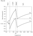
- FIG. 32 is an energy band diagram showing an energy distribution of the preferred embodiment.
- FIG. 35 is an electric field intensity distribution diagram showing an electric field intensity distribution in the case where the gate insulating film is constituted of SiO 2 .
- the terminal frame 2 has the form of a plate made of a metal.
- the terminal frame 2 includes a base portion 5 (island), supporting the nitride semiconductor device 3 , a drain terminal 6 , a source terminal 7 , and a gate terminal 8 .
- the drain terminal 6 is formed integral to the base portion 5 .
- the drain terminal 6 , the source terminal 7 , and the gate terminal 8 are electrically connected respectively by bonding wires 9 to 11 to a drain, a source, and a gate of the nitride semiconductor device 3 .
- the source terminal 7 and the gate terminal 8 are disposed so as to sandwich the drain terminal 6 at a center.
- the resin package 4 is constituted, for example, of a known molding resin, such as an epoxy resin, etc., and seals the nitride semiconductor device 3 .
- the resin package 4 covers the nitride semiconductor device 3 together with the base portion 5 of the terminal frame 2 and the bonding wires 9 to 11 . Portions of the three terminals 6 to 8 are exposed from the resin package 4 .
- FIG. 2 is a schematic sectional view of the nitride semiconductor device 3 of FIG. 1 .
- FIG. 2 does not show a section plane at a specific position of FIG. 1 but shows an assembly of elements, considered necessary for describing the present preferred embodiment, in a single section.
- the nitride semiconductor device 3 includes a substrate 12 , an electron transit layer 13 on the substrate 12 , and an electron supply layer 14 on the electron transit layer 13 .
- the electron transit layer 13 and the electron supply layer 14 are formed on the substrate 12 , for example, by an epitaxial growth method.
- a buffer layer constituted of AlN or AlGaN, etc., may be interposed as necessary between the substrate 12 and the electron transit layer 13 .
- the substrate 12 may, for example, be a conductive silicon substrate.
- the conductive silicon substrate may have an impurity concentration, for example, of 1 ⁇ 10 17 cm ⁇ 3 to 1 ⁇ 10 20 cm ⁇ 3 (and more specifically, approximately 1 ⁇ 10 18 cm ⁇ 3 ).
- the gate layer 15 may, for example, be an undoped GaN layer.
- undoped GaN signifies GaN that effectively does not contain an acceptor type impurity and is specifically GaN with which an impurity is not intentionally introduced when forming the gate layer 15 and is more specifically GaN with a concentration of, for example, less than 1 ⁇ 10 17 cm ⁇ 3 and more preferably less than 1 ⁇ 10 16 cm ⁇ 3 . This is because if the impurity concentration contained in the gate layer 15 is of approximately such level, the impurity will not function as an acceptor.
- the impurity concentrations may be determined by performing SIMS (secondary ion mass spectroscope) analysis on the gate layer 15 .
- the electron transit layer 13 is constituted of a GaN layer
- the electron supply layer 14 is constituted of an Al x Ga 1-x N layer (0 ⁇ x ⁇ 1).
- the electron transit layer 13 and the electron supply layer 14 are thus constituted of nitride semiconductors that differ mutually in composition and form a heterojunction. Therefore, as shown in FIG. 3 , in addition to spontaneous polarizations P sp(GaN) and P sp(AlGaN) occurring in the layers 13 and 14 due to configurations of respective atoms in interiors of crystal structures, a piezo polarization P px(AlGaN) , due to lattice mismatch of the two, occurs in the electron supply layer 14 .
- positive polarization charges 20 Due to these polarizations positive polarization charges 20 , shown in FIG. 3 , are generated in a portion of the electron supply layer 14 near an interface (GaN/AlGaN heterointerface) with the electron transit layer 13 .
- the magnitude (P) of the polarization charges 20 is expressed by the following formula (2) using the abovementioned spontaneous polarizations and the piezo polarization and, as shown in FIG. 4 , increases substantially linearly in proportion to an Al composition of the electronic supply layer 14 (AlGaN).
- P P sp(AlGaN) +P pz(AlGaN) ⁇ P sp(GaN) (2)
- a large internal electric field is generated due to the polarization charges 20 and a two-dimensional electron gas 21 spreads as shown in FIG. 2 .
- the source electrode 18 and the drain electrode 19 are ohmic electrodes, containing, for example, Ti and Al, and are electrically connected to the two-dimensional electron gas 21 via the electron supply layer 14 .
- the bonding wires 9 to 11 are connected respectively to the drain electrode 19 , the source electrode 18 , and the gate electrode 16 .
- a rear surface electrode 22 is formed on a rear surface of the substrate 12 and the substrate 12 is connected to the base portion 5 via the rear surface electrode 22 . Therefore, with the present preferred embodiment, the substrate 12 is electrically connected to the drain electrode 19 via the bonding wire 9 and thereby set at a drain potential.
- FIG. 5 is an energy band diagram of the nitride semiconductor device 3 .
- FIG. 6 is a diagram of electric field intensity distribution of the nitride semiconductor device 3 .
- the positive polarization charges 20 are generated in the portion of the electron supply layer 14 near the interface (GaN/AlGaN heterointerface) with the electron transit layer 13 .
- the entire system of the junction (AlGaN/GaN junction) of the electron supply layer 14 and the electron transit layer 13 positive spatial charges are canceled out by negative spatial charges so that the total of the spatial charges is zero and therefore in correspondence to the positive polarization charges 20 inside the electron supply layer 14 , the two-dimensional electron gas 21 , constituted of negative spatial charges, is generated in the electron transit layer 13 (GaN) that has a bandgap smaller than the electron supply layer 14 (AlGaN).
- the two-dimensional electron gas 21 serves as a passage (channel) for electrons between the source and the drain.
- a so-called normally-on type arrangement is realized in which a current flows between the source and the drain due to a potential difference between the source and the drain even when a voltage is not applied to the gate electrode 16 .
- the gate layer 15 constituted of GaN, which has a smaller bandgap than the electron supply layer 14 (AlGaN), and effectively not containing an acceptor type impurity, is interposed between the electron supply layer 14 and the gate electrode 16 to realize a normally-off type device.
- the mechanism by which a normally-off arrangement is realized in the present invention is as follows. That is, in principle, the positive polarization charges 20 are canceled out by a spontaneous polarization P sp(GaN-Gate) occurring inside the gate layer 15 and consequently, the two-dimensional electron gas 21 is eliminated selectively from a gate region Ga in which the gate electrode 16 is disposed. That is, it suffices to provide an arrangement where the spontaneous polarization (—P sp(GaN-Gate) ) of the gate layer 15 is added to the formula (2) above and the magnitude P of the polarization charges 20 is as indicated by the following formula (3).
- the conditions are set so that in FIG. 5 , (P2)+(P3) ⁇ (P1)>0 is satisfied for increments/decrements (P1), (P2), and (P3) of the potential of a conduction band E C between the gate electrode 16 and a potential well 23 , formed at the junction interface (GaN/AlGaN interface) of the electron transit layer 13 and the electron supply layer 14 .
- This is because it will thereby become necessary to apply a positive voltage to the gate electrode 16 to lower the potential of the conduction band E C of the potential well 23 to a position lower than a Fermi level (at the position of 0.0 eV in FIG. 5 ) and make the drain current flow.
- FIG. 5 shows an energy band when a threshold voltage Vth of 1.0 V is applied to the gate electrode 16 and by setting the gate voltage ⁇ 1.0 V (gate on), the potential of the conduction band E C of the potential well 23 becomes equivalent to the Fermi level so that electrons fall into the potential well 23 (the two-dimensional electron gas 21 begins to be generated in the gate region Ga) and the drain current begins to flow. That is, in a state where a voltage is not applied to the gate electrode 16 (gate off), the potential of the conduction band E C of the potential well 23 ′ is at a position higher than the Fermi level as indicated by an alternate long and short dashed line in FIG. 5 and is in a state where the drain current does not flow.
- the ordinate indicates the potential with respect to electrons.
- FIG. 6 when expressed as an electric field intensity distribution, the conditions of FIG. 5 will be as shown in FIG. 6 .
- a black solid line indicates the electric field intensities at the respective layers when the threshold voltage Vth of 1.0 V is applied to the gate electrode 16 .
- an electric field intensity integration value A (hatched portion in FIG. 6 ) of the AlGaN electron supply layer 14 and an electric field intensity integration value B (cross-hatched portion in FIG. 6 ) of the GaN gate layer 15 satisfy B>A to realize a normally-off arrangement.
- the internal electric field of the electron supply layer 14 is thereby canceled out by the internal electric field of the gate layer 15 and therefore the generation of the two-dimensional electron gas 21 is suppressed.
- the first term, the second term, and the third term from the left respectively correspond to the decrement (P2), the decrement (P3), and the increment (P1) of the potential of the conduction band E C .
- the definitions of the respective symbols in the formula (1) are as follows.
- ⁇ B work function (eV) of the gate electrode 16 —electron affinity (3.6 eV) of GaN
- E F energy difference (eV) between the Fermi level and a lower end of conduction band (E C ) of the electron transit layer 13
- d B P/ ⁇ 0 ⁇ B corresponding to the increment (P1) of the potential of the conduction band E C .
- d B P/ ⁇ 0 ⁇ B which is the increment (P1) of the potential of the conduction band E C , increases proportionally with an increase in the thickness d B of the electron supply layer 14 and therefore in regard to d B P/ ⁇ 0 ⁇ B , it is preferable for the thickness d B to be as small as possible. Therefore, although when the thickness d B exceeds 20 nm, a satisfactory sheet carrier density can be achieved, the increment (P1) of the potential of the conduction band E C becomes large, and it is thus preferable for the thickness d B of the electron supply layer 14 to be not more than 20 nm and not more than 30 nm at the most.
- the sheet carrier density is in a vicinity of 8.0 ⁇ 10 12 (cm ⁇ 2 ) or less.
- the sheet carrier density is approximately 8.0 ⁇ 10 12 (cm ⁇ 2 ) if the Al composition is approximately 0.25, and it is therefore preferable for the Al composition to be not more than 0.25 (not more than 25%).
- the sheet carrier density can be made 8.0 ⁇ 10 12 (cm ⁇ 2 ) as long as the film thickness d B of the AlGaN electron supply layer 14 is small.
- the upper side is a range in which a normally-off arrangement can be realized and the lower side is a range in which a normally-on arrangement is realized. Therefore, for each thickness d B and Al composition of the electron supply layer 14 , the value of d G ⁇ square root over (N DA +N A ⁇ N DD ⁇ N D ) ⁇ is set as suited so as to be included in the range higher than the corresponding graph in FIG. 9 .
- a shallow donor level E D a deep donor level E DD , a shallow acceptor level E A , and a deep acceptor level E DA are formed.
- the deep donor level E DD is, for example, an energy level at a position separated by not less than 0.025 eV from the lower end (bottom) energy level E C of the conduction band of the electron transit layer 13 . That is, the deep donor level E DD is formed by doping of a donor, with which an ionization energy necessary for excitation is greater than the thermal energy at room temperature. Therefore, ordinarily, the donor electrons doped at this position are not excited to the conduction band and are in a state of being captured by the donor at room temperature.
- the deep donor level E DD may, for example, be that due to a crystal defect occurring spontaneously in GaN during epitaxial growth of the electron transit layer 13 .
- the shallow acceptor level E A is, for example, an energy level at a position separated by not more than 0.025 eV from an upper end (top) energy level E V of valence electrons of the electron transit layer 13 and may be referred to simply as the “acceptor level E A ” as long as distinction can be made with respect to the deep acceptor level E DA .
- acceptor level E A an energy level at a position separated by not more than 0.025 eV from an upper end (top) energy level E V of valence electrons of the electron transit layer 13 and may be referred to simply as the “acceptor level E A ” as long as distinction can be made with respect to the deep acceptor level E DA .
- an impurity doped into the electron transit layer 13 constituted of GaN, to form the deep acceptor level E DA
- at least one type selected from the group consisting of C, Be, Cd, Ca, Cu, Ag, Au, Sr, Ba, Li, Na, K, Sc, Zr, Fe, Co, Mi, Mg, Ar, and He can be cited.
- C may also be used as the deep acceptor.
- C When C is used for the deep acceptor level, it is known to form, for example, a level of 0.9 eV from the upper end (top) energy E V of the valence band of the electron transit layer 13 .
- E V the upper end (top) energy
- Mg Mg
- it is known to form a level of 0.1 to 0.2 eV from E V .
- Concentrations of the impurities (dopants) forming the shallow donor level E D , the deep donor level E DD , the shallow acceptor level E A , and the deep acceptor level E DA described above shall be referred to respectively as a shallow donor concentration N D , a deep donor concentration N DD , a shallow acceptor concentration N A , and a deep acceptor concentration N DA .
- a shallow donor concentration N D a deep donor concentration
- N DD a deep donor concentration
- N A shallow acceptor concentration
- N DA a deep acceptor concentration N DA
- concentrations N D , N DD , N A , and N DA may be measured, for example, by SIMS (Secondary ion Mass Spectrometry).
- FIG. 10A when a voltage is not applied across both electrodes (unbiased state), the acceptors and the deep acceptors capture electrons emitted by the donors and the deep donors. In this state, positive charges, due to the donors and the deep donors that emitted the electrons, and negative charges, due to the acceptors and the deep acceptors that captured the electrons, are equal in number and therefore the GaN layer is electrically neutral as a whole.
- the preferable ranges of d G ⁇ square root over (N DA +N A ⁇ N DD ⁇ N D ) ⁇ for the respective thicknesses d B and Al compositions of the electron supply layer 14 are as shown in FIG. 9 , and preferable ranges of d G and (N DA +N A ⁇ N DD ⁇ N D ) that constitute d G ⁇ square root over (N DA +N A ⁇ N DD ⁇ N D ) ⁇ are, for example, as indicated below.
- the preferable ranges indicated below differ according to the respective thicknesses d B and Al compositions of the electron supply layer 14 and may therefore be set as suited in accordance with the respective thicknesses d B and Al compositions of the electron supply layer 14 .
- the thickness d G of the gate layer 15 is preferably, for example, 50 nm to 100 nm.
- (N DA +N A ⁇ N DD ⁇ N D ) is not less than 5 ⁇ 10 16 cm ⁇ 3 . This preferable range of (N DA +N A ⁇ N DD ⁇ N D ) can be explained with reference to FIG. 11 .
- the threshold voltage in this state is 0.3 eV and a normally-off operation is narrowly realized. From this, it can be understood that for a normally-off operation, (N DA +N A ⁇ N DD ⁇ N D ) of at least 5 ⁇ 10 16 cm ⁇ 3 is necessary.
- ⁇ B work function (eV) of the gate electrode 16 —electron affinity (3.6 eV) of GaN
- ⁇ B work function (eV) of the gate electrode 16 —electron affinity (3.6 eV) of GaN
- the electron transit layer 13 is constituted of GaN and the electron supply layer 14 is constituted of AlGaN was described, it suffices that the electron transit layer 13 and the electron supply layer 14 differ in Al composition and other combinations are also possible.
- the electron supply layer/electron transit layer combination may be any of AlGaN layer/GaN layer, AlGaN layer/AlGaN layer (with the layers differing in Al composition), AlInN layer/AlGaN layer, AlInN layer/GaN layer, AlN layer/GaN layer, and AlN layer/AlGaN layer.
- the electron supply layer contains Al and N in its composition.
- the electron transit layer contains Ga and N in its composition and differs in Al composition from the electron supply layer.
- the electron supply layer and the electron transit layer differing in Al composition a lattice mismatch arises between the two and carriers due to polarization are thereby made to contribute to the forming of a two-dimensional electron gas.
- silicon was taken up as an example of the material of the substrate 12 , besides this, any substrate material, such as a sapphire substrate, a GaN substrate, etc., may be applied.
- a second preferred embodiment and a third preferred embodiment of the first invention shall now be described in detail with reference to FIG. 1 to FIG. 8 , FIG. 10 , and FIG. 18 to FIG. 24 .
- An external view of a semiconductor package 1 that includes a nitride semiconductor device 3 according to the second preferred embodiment is the same as the external view of the semiconductor package 1 that includes the nitride semiconductor device 3 according to the first preferred embodiment of the first invention described using FIG. 1 .
- the semiconductor package 1 which includes the nitride semiconductor device 3 according to the second preferred embodiment, includes a terminal frame 2 , the nitride semiconductor device 3 (chip), and a resin package 4 .
- a schematic sectional view of the nitride semiconductor device 3 according to the second preferred embodiment is the same as the schematic sectional view of the nitride semiconductor device 3 according to the first preferred embodiment described using FIG. 2 .
- the nitride semiconductor device 3 includes a substrate 12 , an electron transit layer 13 on the substrate 12 , and an electron supply layer 14 on the electron transit layer 13 .
- the electron transit layer 13 and the electron supply layer 14 are formed on the substrate 12 , for example, by an epitaxial growth method.
- a buffer layer constituted of AlN or AlGaN, etc., may be interposed as necessary between the substrate 12 and the electron transit layer 13 .
- the nitride semiconductor device 3 further includes a gate layer 15 , formed selectively on the electron supply layer 14 , and a gate electrode 16 , formed on the gate layer 15 .
- the gate electrode 16 faces the electron supply layer 14 via the gate layer 15 .
- a surface insulating film 17 is formed on the electron supply layer 14 so as to cover the gate electrode 16 .
- the source electrode 18 and the drain electrode 19 are disposed across an interval and the gate electrode 16 is disposed therebetween. Also, the source electrode 18 is formed in a pattern that covers the gate electrode 16 via the surface insulating film 17 .
- the substrate 12 may, for example, be a conductive silicon substrate.
- the conductive silicon substrate may have an impurity concentration, for example, of 1 ⁇ 10 17 cm ⁇ 3 to 1 ⁇ 10 20 cm ⁇ 3 (and more specifically, approximately 1 ⁇ 10 18 cm ⁇ 3 ).
- the gate layer 15 may, for example, be an undoped GaN layer or may be a GaN layer containing an acceptor type level.
- undoped GaN signifies GaN that effectively does not contain an acceptor type impurity.
- it is GaN with which an impurity is not intentionally introduced when forming the gate layer 15 and is more specifically GaN with a concentration of, for example, less than 1 ⁇ 10 17 cm ⁇ 3 and more preferably less than 1 ⁇ 10 16 cm ⁇ 3 . This is because if the impurity concentration contained in the gate layer 15 is of approximately such level, the impurity will not function as an acceptor.
- the impurity concentrations may be determined by performing SIMS (secondary ion mass spectroscope) analysis on the gate layer 15 .
- the GaN layer that includes the acceptor type level may contain, for example, Mg or C as the acceptor or may have a hole defect formed therein.
- the electron transit layer 13 is constituted of a GaN layer
- the electron supply layer 14 is constituted of an Al x Ga 1-x N layer (0 ⁇ x ⁇ 1) and may contain In as necessary.
- the electron transit layer 13 and the electron supply layer 14 are thus constituted of nitride semiconductors that differ mutually in composition and form a heterojunction. Therefore, as shown in FIG. 3 , in addition to spontaneous polarizations P sp(GaN) and P sp(AlGaN) occurring in the layers 13 and 14 due to configurations of respective atoms in interiors of crystal structures, a piezo polarization P pz(AlGaN) , due to lattice mismatch of the two, occurs in the electron supply layer 14 .
- positive polarization charges 20 are generated in a portion of the electron supply layer 14 near an interface (GaN/AlGaN heterointerface) with the electron transit layer 13 .
- the magnitude (P) of the polarization charges 20 is expressed by the following formula (2) using the spontaneous polarizations and the piezo polarization and, as shown in FIG. 4 , increases substantially linearly in proportion to the Al composition of the electronic supply layer 14 (AlGaN).
- P P sp(AlGaN) +P pz(AlGaN) ⁇ P sp(GaN) (2)
- a large internal electric field is generated due to the polarization charges 20 and a two-dimensional electron gas 21 spreads as shown in FIG. 2 .
- the source electrode 18 and the drain electrode 19 are ohmic electrodes, containing, for example, Ti and Al, and are electrically connected to the two-dimensional electron gas 21 .
- the bonding wires 9 to 11 are connected respectively to the drain electrode 19 , the source electrode 18 , and the gate electrode 16 .
- a rear surface electrode 22 is formed on a rear surface of the substrate 12 and the substrate 12 is connected to the base portion 5 via the rear surface electrode 22 . Therefore, with the present preferred embodiment, the substrate 12 is electrically connected to the drain electrode 19 via the bonding wire 9 and thereby set at the drain potential.
- FIG. 5 is an energy band diagram of the nitride semiconductor device 3 .
- FIG. 6 is a diagram of the electric field intensity distribution of the nitride semiconductor device 3 .
- the positive polarization charges 20 are generated in the portion of the electron supply layer 14 near the interface (GaN/AlGaN heterointerface) with the electron transit layer 13 .
- the entire system of the junction (AlGaN/GaN junction) of the electron supply layer 14 and the electron transit layer 13 positive spatial charges are canceled out by negative spatial charges so that the total of the spatial charges is zero and therefore in correspondence to the positive polarization charges 20 inside the electron supply layer 14 , the two-dimensional electron gas 21 , constituted of negative spatial charges, is generated in the electron transit layer 13 (GaN) that has a bandgap smaller than the electron supply layer 14 (AlGaN).
- the two-dimensional electron gas 21 serves as a passage (channel) for electrons between the source and the drain.
- a so-called normally-on type arrangement is realized in which a current flows between the source and the drain due to the potential difference between the source and the drain even when a voltage is not applied to the gate electrode 16 .
- the gate layer 15 constituted of GaN, which has a smaller bandgap than the electron supply layer 14 (AlGaN), and effectively not containing an acceptor type impurity, is interposed between the electron supply layer 14 and the gate electrode 16 to realize a normally-off type device.
- the magnitude of the polarization charges 20 is dependent on the Al composition of the electron supply layer 14 (AlGaN) as shown in FIG. 4 .
- the ordinate indicates the potential with respect to electrons.
- FIG. 6 when expressed as an electric field intensity distribution, the conditions of FIG. 5 will be as shown in FIG. 6 .
- the black solid line indicates the electric field intensities at the respective layers when the threshold voltage Vth of 1.0 V is applied to the gate electrode 16 .
- an electric field intensity integration value A (hatched portion in FIG. 6 ) of the AlGaN electron supply layer 14 and an electric field intensity integration value B (cross-hatched portion in FIG. 6 ) of the GaN gate layer 14 satisfy B>A to realize a normally-off arrangement.
- the internal electric field of the electron supply layer 14 is thereby canceled out by the internal electric field of the gate layer 15 and therefore the generation of the two-dimensional electron gas 21 is suppressed.
- the first term, the second term, and the third term from the left respectively correspond to the decrement (P2), the decrement (P3), and the increment (P1) of the potential of the conduction band E C .
- the definitions of the respective symbols in the formula (1) are as follows.
- ⁇ B work function (eV) of the gate electrode 16 —electron affinity (3.6 eV) of GaN
- E F energy difference (eV) between the Fermi level and a lower end of conduction band (E C ) of the electron transit layer 13
- N DA +N A ⁇ N DD ⁇ N D of d G ⁇ square root over (N DA +N A ⁇ N DD ⁇ N D ) ⁇ , which, in the formula (1), is a portion of the decrement (P2) of the potential of the conduction band E C , may be determined as follows.
- a shallow donor level E D a deep donor level E DD , a shallow acceptor level E A , and a deep acceptor level E DA are formed.
- the shallow donor level E D is, for example, an energy level at a position separated by not more than 0.025 eV from the lower end (bottom) energy level E C of the conduction band of the electron transit layer 13 and may be referred to simply as the “donor level E D ” as long as distinction can be made with respect to the deep donor level E DD .
- As an impurity forming the shallow donor level E D for example, at least one type selected from the group consisting of Si and O can be cited. These may be incorporated into the film during epitaxial growth of the electron transit layer 13 or may be doped intentionally. For example, oxygen (O) maybe incorporated from a raw material gas or a carrier gas.
- the deep donor level E DD is, for example, an energy level at a position separated by not less than 0.025 eV from the lower end (bottom) energy level E C of the conduction band of the electron transit layer 13 . That is, the deep donor level E DD is formed by doping of a donor, with which an ionization energy necessary for excitation is greater than the thermal energy at room temperature. Therefore, ordinarily, the donor electrons doped at this position are not excited to the conduction band and are in a state of being captured by the donor at room temperature.
- the deep donor level E DD may, for example, be that due to a crystal defect occurring spontaneously in GaN during epitaxial growth of the electron transit layer 13 .
- the shallow acceptor level E A is, for example, an energy level at a position separated by not more than 0.025 eV from an upper end (top) energy level E V of valence electrons of the electron transit ever 13 and may be referred to simply as the “acceptor level E A ” as long as distinction can be made with respect to the deep acceptor level E DA .
- the deep acceptor level E DA is, for example, an energy level at a position separated by not less than 0.025 eV from the upper end (top) energy level E V of the valence electrons of the electron transit layer 13 . That is, the deep acceptor level E DA is formed by doping of an acceptor, with which an ionization energy necessary for excitation is greater than the thermal energy at room temperature. Therefore ordinarily, the acceptor holes doped at this position are not excited to the valence band and are in a state of being captured by the acceptor at room temperature.
- an impurity doped into the electron transit layer 13 constituted of GaN, to form the deep acceptor level E DA
- at least one type selected from the group consisting of C, Be, Cd, Ca, Cu, Ag, Au, Sr, Ba, Li, Na, K, Sc, Zr, Fe, Co, Ni, Mg, Ar, and He can be cited.
- C and Mg can be cited mainly, carbon (C) functions as a deep acceptor when incorporated in a nitrogen site inside GaN and functions as a shallow donor when incorporated in a Ga site, and therefore, to increase (N DA +N A ⁇ N DD ⁇ N D ) reliably, it is preferable to use Mg.
- a region of the electron transit layer 13 in which the energy band is curved depends on the type (Fermi level) of impurity and (N DA +N A ⁇ N DD ⁇ N D ).
- the region of the electron transit layer 13 in which Mg is cont fined depends on the Mg concentration. For example, in FIG.
- the impurity is Mg and (N DA +N A ⁇ N DD ⁇ N D ) is 1 ⁇ 10 17 cm ⁇ 3
- the region of the GaN electron transit layer 13 in which the energy band is curved is approximately 150 nm from the AlGaN electron supply layer 14 /GaN electron transit layer 13 interface.
- the impurity is Mg and (N DA +N A ⁇ N DD ⁇ N D ) is 4 ⁇ 10 16 cm ⁇ 3
- the region in which the energy band is curved is approximately 250 nm from the AlGaN electron supply layer 14 /GaN electron transit layer 13 interface. That is, this is because the region within the abovementioned upper limit from the AlGaN electron supply layer 14 /GaN electron transit layer 13 interface contributes to the threshold voltage and the concentrations and types of impurities in this region are important.
- the leak current is increased by the formed hole acting as a carrier.
- Concentrations of the impurities (dopants) forming the shallow donor level E D , the deep donor level E DD , the shallow acceptor level E A , and the deep acceptor level E DA described above shall be referred to respectively as a shallow donor concentration N D , a deep donor concentration N DD , a shallow acceptor concentration N A , and a deep acceptor concentration N DA .
- a shallow donor concentration N D a deep donor concentration
- N DD a deep donor concentration
- N A shallow acceptor concentration
- N DA a deep acceptor concentration N DA
- concentrations N D , N DD , N A , and N DA may be measured, for example, by SIMS (Secondary Ion Mass Spectrometry).
- FIG. 10A when a voltage is not applied across both electrodes (unbiased state), the acceptors and the deep acceptors capture electrons emitted by the donors and the deep donors. In this state, positive charges, due to the donors and the deep donors that emitted the electrons, and negative charges, due to the acceptors and the deep acceptors that captured the electrons, are equal in number and therefore the GaN layer is electrically neutral as a whole.
- Preferable ranges of d G and (N DA +N A ⁇ N DD ⁇ N D ) that constitute d G ⁇ square root over (N DA +N A ⁇ N DD ⁇ N D ) ⁇ are, for example, as indicated below.
- the preferable ranges indicated below differ according to the respective thicknesses d B and Al compositions of the electron supply layer 14 and may therefore be set as suited in accordance with the respective thicknesses d B and Al compositions of the electron supply layer 14 .
- the thickness d G of the gate layer 15 is preferably, for example, 50 nm to 200 nm.
- (N DA +N A ⁇ N DD ⁇ N D ) of the electron transit layer 13 is, for example, 1 ⁇ 10 16 cm ⁇ 3 to 5 ⁇ 10 17 cm ⁇ 3 and preferably, the Mg concentration is not less than 1 ⁇ 10 16 cm ⁇ 3 and more preferably, the Mg concentration is not more than 1 ⁇ 10 17 cm ⁇ 3 .
- ⁇ B work function (eV) of the gate electrode 16 —electron affinity (3.6 V) of GaN
- ⁇ B work function (eV) of the gate electrode 16 —electron affinity (3.6 V) of GaN
- d B P/ ⁇ 0 ⁇ B corresponding to the increment (P1) of the potential of the conduction band E C .
- d B P/ ⁇ 0 ⁇ B which is the increment (P1) of the potential of the conduction band E C , increases proportionally with an increase in the thickness d B of the electron supply layer 14 and therefore if making d B P/ ⁇ 0 ⁇ B small is considered with priority, it is preferable for the thickness d B to be as small as possible. It is thus preferable for the thickness d B of the electron supply layer 14 to be as small as possible within a range of not more than 10 nm.
- the sheet carrier density decreases.
- the decrease is especially significant in a region of d B ⁇ 5 nm.
- the sheet carrier density is preferably, for example, not less than 6.0 ⁇ 10 12 cm ⁇ 2 because if it is too low, channel mobility decreases.
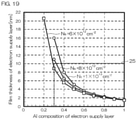
- the Al composition of the electron supply layer 14 should thus be set in a range of not more than 10 nm along the abscissa and not less than 6.0 ⁇ 10 12 cm ⁇ 2 along the ordinate in FIG. 7 .
- the Al composition is in a proportional relationship with the variable P in d B P/ ⁇ 0 ⁇ B , which corresponds to the increment (P1) of the potential of the conduction band E C and, depending on the case, influences the gate threshold voltage. Relationships of the Al composition of the electron supply layer 14 and the gate threshold voltage were thus examined.
- FIG. 18 is a diagram showing relationships of the Al composition of the electron supply layer 14 and the gate threshold voltage according to sheet carrier density.
- FIG. 19 is a diagram showing relationships of the Al composition of the electron supply layer 14 and the film thickness of the electron supply layer 14 according to sheet carrier density. In FIG. 18 and FIG. 19 , calculations were made with the deep acceptor concentration of the gate layer 15 being set to 2 ⁇ 10 17 cm ⁇ 3 and the deep acceptor concentration of the electron transit layer 13 being set to 4 ⁇ 10 16 cm ⁇ 3 .
- the electron supply layer 14 is to be made an AlN layer, it is preferable to dispose an etching stop layer 24 , constituted of Al x′ GA 1-x′ N (x′ ⁇ 1), on the electron supply layer 14 as shown in FIG. 20 .
- the AlN electron supply layer 14 is thereby covered by etching stop layer 24 in the process of etching the gate layer 15 and the oxidation of the AlN electron supply layer 14 can thus be suppressed.
- the effect of suppressing the oxidation of the electron supply layer 14 such as described above is not restricted to an AlN layer and can be achieved when the etching stop layer 24 , constituted of Al x′ Ga 1-x′ N (x′ ⁇ 1), is formed on an electron supply layer 14 constituted of Al x′ Ga 1-x N (x ⁇ 1) and a relationship, x ⁇ x′, is further established in regard to the Al composition.
- the etching stop layer 24 and the electron supply layer 14 are further removed selectively so as to be continuous with the contact holes 18 a and 19 a, and the source electrode 18 and the drain electrode 19 are out in ohmic contact with the electron transit layer 13 via the contact holes 18 a and 19 a.
- the electron transit layer 13 , the electron supply layer 14 , the etching stop layer 24 , and the gate layer 15 are formed on the substrate 12 , for example, by an epitaxial growth method.
- an electrode material 26 of the gate electrode 16 is formed on the gate layer 15 .
- the electrode material 26 is etched selectively to form the gate electrode 16 .
- the gate layer 15 is etched selectively using, for example, a Cl 2 /O 2 plasma. The etching stops at the AlGaN etching stop layer 24 .
- the surface insulating film 17 constituted, for example, of SiN, is formed so as to cover the etching stop layer 24 , the gate layer 15 , and the gate electrode 16 .
- the surface insulating film 17 , the etching stop layer 24 , and the electron supply layer 14 are continuously etched selectively to form the contact holes 18 a and 19 a.
- contact resistances of the source electrode 18 and the drain electrode 19 can be reduced by etching the electron supply layer 14 as well to expose the electron transit layer 13 .
- the source electrode 18 and the drain electrode 19 are formed By thereafter forming the rear surface electrode 22 , etc., the nitride semiconductor device 3 is obtained.
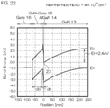
- FIG. 22 to FIG. 26 are diagrams of GaN Fermi level dependence of the gate threshold voltage.
- FIG. 24 is an energy band diagram of a turn-on state under conditions that are the same as those of FIG. 22 with the exception that N DA +N A ⁇ N DD ⁇ N D of the electron transit layer 13 is 1 ⁇ 10 17 cm ⁇ 3 .
- FIG. 25 is an energy band diagram of a turn-on state under conditions that are the same as those of FIG. 23 with the exception that N DA +N A ⁇ N DD ⁇ N D of the electron transit layer 13 i s 1 ⁇ 10 17 cm ⁇ 3 .
- N DA +N A ⁇ N DD ⁇ N D in this case is preferably not less than 1 ⁇ 10 16 cm ⁇ 3 and not more than 1 ⁇ 10 18 cm ⁇ 3 .
- the electron transit layer 13 is constituted of GaN and the electron supply layer 14 is constituted of AlGaN or AlN was described, it suffices that the electron transit layer 13 and the electron supply layer 14 differ in Al composition and other combinations are also possible.
- the electron supply layer/electron transit layer combination may be any of AlGaN layer/GaN layer, AlGaN layer/AlGaN layer (with the layers differing in Al composition), AlInN layer/AlGaN layer, AlInN layer/GaN layer, AlN layer/GaN layer, and AlN layer/AlGaN layer.
- the electron supply layer contains Al and N in its composition.
- the electron transit layer contains Ga and N in its composition and differs in Al composition from the electron supply layer.
- the electron supply layer and the electron transit layer differing in Al composition a lattice mismatch arises between the two and carriers due to polarization are thereby made to contribute to the forming of a two-dimensional electron gas.
- the electron supply layer 14 is Al x Ga 1-x N (x ⁇ 1) was mainly described, in a case where the electron supply layer 14 contains.
- x, and y may be such that x ⁇ 0.3, 0.02 ⁇ y ⁇ 0, and 1 ⁇ x+y.
- silicon was taken up as an example of the material of the substrate 12 , besides this, any substrate material, such as a sapphire substrate, a GaN substrate, etc., may be applied.
- the second invention relates to a nitride semiconductor device constituted of a group III nitride semiconductor (may hereinafter be referred to simply as “nitride semiconductor” in some cases).
- a group III nitride semiconductor is a semiconductor with which nitrogen is used as a group V element in a group III-V semiconductor.
- Representative examples are aluminum nitride (AlN), gallium nitride (GaN), and indium nitride (InN).
- AlN aluminum nitride
- GaN gallium nitride
- InN indium nitride
- the semiconductor can be expressed generally as Al x In y Ga 1-x-y N (0 ⁇ x ⁇ 1, 0 ⁇ y ⁇ 1, 0 ⁇ x+y ⁇ 1).
- Such an HEMT includes, for example, an electron transit layer, constituted of GaN, and an electron supply layer, constituted of AlGaN that is grown epitaxially on the electron transit layer.
- a pair of source electrode and drain electrode are formed to be in contact with the electron supply layer and a gate electrode is disposed therebetween. Due to polarization caused by lattice mismatch of GaN and AlGaN, a two-dimensional electron gas is formed inside the electron transit layer at a position located only a few ⁇ inward from an interface of the electron transit layer and the electron supply layer.
- the source and the crain are connected to each other with the two-dimensional electron gas as a channel.
- the source and the drain are cut off from each other.
- the source and the drain are continuous to each other in a state where the control voltage is not applied to the gate electrode and therefore the device is of the normally-on type.
- Devices using a nitride semiconductor have features of high withstand voltage, high temperature operation, high current density, high speed switching, and low on resistance and are thus being examined for application to power devices.
- a device for use as a power device, a device must be of the normally-off type, in which current is cut off in a zero bias state, and therefore an HEMT such as described above cannot be applied to a power device.
- Japanese Patent Application Publication No. 2006-339561 discloses an arrangement where p type GaN gate layer (nitride semiconductor gate layer ) is laminated on an AlGaN electron supply layer, a gate electrode is disposed thereon, and the channel is eliminated by a depletion layer spreading from the p type GaN gate layer to realize a normally-off arrangement.
- a gate electrode constituted of Pd (palladium) in ohmic junction with the p type GaN gate layer, is used as the gate electrode.
- a gate electrode constituted of TiN (titanium nitride) or other metal in Schottky junction with the p type GaN gate layer, as the gate electrode may be considered.
- a nitride semiconductor device of such an arrangement may be referred to in some cases as a compared device. With the compared device, there is a problem in that due to the nitride semiconductor gate layer and the gate electrode being in Schottky junction, a gate leak current becomes large and the nitride semiconductor gate layer degrades readily.
- An object of the second invention is to provide a nitride semiconductor device with which the gate leak current can be reduced in comparison to the compared device.
- the second invention has the following features.
- a nitride semiconductor device including a first nitride semiconductor layer, constituting an electron transit layer, a second nitride semiconductor layer, formed on the first nitride semiconductor layer, being larger in bandgap than the first nitride semiconductor layer, and constituting an electron supply layer, and a gate portion, disposed on the second nitride semiconductor layer, and where the gate portion includes a nitride semiconductor gate layer, disposed on the second nitride semiconductor layer and containing an acceptor type impurity, a gate insulating formed on the nitride semiconductor gate layer, and a gate electrode, formed on the gate insulating film.
- the gate insulating film is interposed between the nitride semiconductor gate layer and the gate electrode, and the gate leak current can thus be reduced in comparison to the compared device.
- A4 The nitride semiconductor device according to any one of “A1.” to “A3.,” where the gate leak current is not more than 1 nA/mm.
- A5. The nitride semiconductor device according to any one of “A1.” to “A3., ” where the nitride semiconductor gate layer has a film thickness of not more than 100 nm and the gate insulating film has a film thickness of not less than 3 nm.
- the nitride semiconductor device according to any one of “A1.”to “A5.,” further including a third nitride semiconductor layer, disposed at a side of the first nitride semiconductor layer opposite the second nitride semiconductor layer side and constituting a buffer layer.
- A7 The nitride semiconductor device according to “A1.,” where a carbon concentration of an interface of the nitride semiconductor gate layer and the gate insulating film is not more than 1 ⁇ 10 13 cm ⁇ 2 .
- A8 The nitride semiconductor device according to any one of “A1.” to “A7.,” where the first nitride semiconductor layer is constituted of a GaN layer, the second nitride semiconductor layer is constituted of an AlGaN layer, and the nitride semiconductor gate layer is constituted of a p type GaN layer.
- the nitride semiconductor device according to “A6.”
- the first nitride semiconductor layer is constituted of a GaN layer
- the second nitride semiconductor layer is constituted of an AlGaN layer
- the nitride semiconductor gate layer is constituted of a p type GaN layer
- the third nitride semiconductor layer is constituted of an AlGaN layer.
- FIG. 27 to FIG. 35 A preferred embodiment of the second invention shall be described in detail with reference to FIG. 27 to FIG. 35 .
- the symbols used in FIG. 27 to FIG. 35 are in no relationship with the symbols of FIG. 1 to FIG. 26 used above in the description of the first invention.
- the buffer layer 3 is constituted from a multilayer buffer layer in which a plurality of nitride semiconductor films are laminated.
- the buffer layer 3 is constituted from a first buffer layer A, constituted of an AlN film in contact with the front surface of the substrate 2 , and a second buffer layer 3 B, constituted of an AlGaN film laminated on a front surface of the first buffer layer 3 A (the front surface at the side opposite the substrate 2 side).
- the first buffer layer 3 A has a film thickness of approximately 100 nm to to 300 nm.
- the second buffer layer 3 B has a film thickness of approximately 100 nm to 5 ⁇ m.
- the first nitride semiconductor layer 4 constitutes an electron transit layer.
- the first nitride semiconductor layer 4 is constituted of a GaN layer doped with an acceptor type impurity and has a thickness of approximately 100 nm to 5 ⁇ m.
- the concentration of the acceptor type impurity is preferably not less than 4 ⁇ 10 16 cm ⁇ 3 .
- the acceptor type impurity is C (carbon).
- the first nitride semiconductor layer 4 (electron transit layer) and the second nitride semiconductor layer 5 (electron supply layer) are thus constituted of nitride semiconductors that differ n bandgap (Al composition) and a lattice mismatch occurs therebetween. Due to spontaneous polarizations of the first nitride semiconductor layer 4 and the second nitride semiconductor layer 5 and a piezo polarization due to the lattice mismatch between the two, an energy level of a conduction band of the first nitride semiconductor layer 4 at an interface of the first nitride semiconductor layer 4 and the second nitride semiconductor layer 5 is made lower than a Fermi level.
- a two-dimensional electron gas (2DEG) 16 is thereby made to spread at a position close to the interface of the first nitride semiconductor layer 4 and the second nitride semiconductor layer 5 (for example, at a distance of only several ⁇ from the interface).
- the gate portion 20 includes a nitride semiconductor gate layer 6 , grown epitaxially on the second nitride semiconductor layer 5 , a gate insulating film 7 , formed on the nitride semiconductor gate layer 6 , and a gate electrode 8 , formed on the gate insulating film 7 .
- the nitride semiconductor gate layer 6 is constituted of a nitride semiconductor doped with an acceptor type impurity.
- the nitride semiconductor gate layer 6 is constituted of a GaN layer (p type GaN layer) doped with the acceptor type impurity and has a thickness of approximately 10 nm to 100 nm.
- the film thickness of the nitride semiconductor gate layer 6 is preferably not more than 100 nm. The reason for this shall be described later. In the present preferred embodiment, the film thickness of the nitride semiconductor gate layer 6 is 60 nm.
- the gate insulating film 7 may be constituted from SiN (other than in-situ SiN) SiO 2 , SiON, Al 2 O 3 , AlN, AlON, HfO, HfN, HfON, HfSiON, AlON, etc.
- a carbon concentration of the interface of the nitride semiconductor gate layer 6 and the gate insulating film 7 is not more than 1 ⁇ 10 13 cm ⁇ 2 .
- the gate electrode 8 is formed to be in contact with a front surface of the gate insulating film 7 .
- the gate electrode 8 is constituted from a TiN layer and has a thickness of approximately 50 nm to 200 nm.
- the gate electrode 8 is disposed biasedly toward the source electrode contact hole 11 .
- the barrier metal film 10 is laminated on the passivation film 9 .
- the barrier metal film 10 is constituted of a TiN film and has a thickness of approximately 10 nm to 50 nm. In the present preferred embodiment, the thickness of the barrier metal film 10 is 25 nm.
- the source electrode 13 and the drain electrode 14 are constituted of lower layers (ohmic metal layers) 13 A and 14 A, in contact with the second nitride semiconductor layer 5 , intermediate layers (main electrode metal layers) 13 B and 14 B, laminated on the lower layers 13 A and 14 A, and upper layers (barrier metal layers) 13 C and 14 C, laminated on the intermediate layers 13 B and 14 B.
- the lower layers 13 A and 14 A are, for example, Ti layers with thicknesses of approximately 10 nm to 20 nm.
- the intermediate layers 13 B and 14 B are Al layers with thicknesses of approximately 100 nm to 300 nm.
- the upper layers 13 C and 14 C are, for example, TiN with thicknesses of approximately 10 nm to 50 nm.
- the interlayer insulating film 15 is constituted, for example, of SiO 2 .
- the interlayer insulating film 15 has a thickness of approximately 1 ⁇ m.
- a heterojunction is formed by the second nitride semiconductor layer 5 (electron supply layer), differing in bandgap (Al composition) from the first nitride semiconductor layer 4 (electron transit layer), being formed on the first nitride semiconductor layer 4 .
- the two-dimensional electron gas 16 is thereby formed inside the first nitride semiconductor layer 4 near the interface of the first nitride semiconductor layer 4 and the second nitride semiconductor layer 5 , and an HEMT making use of the two-dimensional electron gas 16 as a channel is formed.
- the gate electrode 8 faces the second nitride semiconductor layer 5 across the gate insulating film 7 and the nitride semiconductor gate layer 6 , constituted of the p type GaN layer.
- the gate electrode 8 energy levels of the first nitride semiconductor layer 4 and the second nitride semiconductor layer 5 are pulled up by the ionized acceptors contained in the nitride semiconductor gate layer 6 , constituted of the p type GaN layer, and therefore the energy level of the conduction band at the heterojunction interface is made higher than the Fermi level. Therefore, the two-dimensional electron gas 16 , due to the spontaneous polarizations of the first nitride semiconductor layer 4 and the second nitride semiconductor layer 5 and the piezo polarization due to the lattice mismatch of the two layers, is not formed directly below the gate electrode 8 (gate portion 20 ).
- a predetermined voltage (for example, of 200 V to 300 V), with which the drain electrode side becomes positive, is applied across the source electrode 13 and the drain electrode 14 .
- an off voltage (0 V) or an on voltage (3 V ) is applied to the gate electrode 8 with the source electrode 13 being at a reference potential (0 V).
- FIG. 28A to FIG. 28G are sectional views for describing an example of a manufacturing process of the nitride semiconductor device 1 described above and show a cross-sectional structure at a plurality of stages in the manufacturing process.
- the buffer layer 3 and the first nitride semiconductor layer (electron transit layer) 4 are successively grown epitaxially on the substrate 2 by an MOCVD (Metal Organic Chemical Vapor Deposition) method. Further, the second nitride semiconductor layer (electron supply layer) 5 is grown epitaxially on the first nitride semiconductor layer 4 by the MOCVD method.
- MOCVD Metal Organic Chemical Vapor Deposition
- a gate layer material film 31 which is a material film of the nitride semiconductor gate layer 6 , is formed on the second nitride semiconductor layer 5 by the MOCVD method.
- an insulating material film 32 which is a material film of the gate insulating film 7 , is formed on the gate layer material film 31 .
- the gate insulating film 7 is constituted SiN
- film formation of the gate insulating film 32 may be performed in succession to and using the same MOCVD device used in film formation of the gate layer material film 31 .
- the insulating material film 32 becomes in-situ SiN, which is formed as a film in-situ with the gate layer material film 31 .
- the insulating material film 32 may also be formed as a film on the gate layer material film 31 by a plasma CVD method. Also, if the gate insulating film 7 is constituted of SiO 2 or other material besides SiN, the insulating material film 32 may be formed as a film on the gate layer material film 31 by the plasma CVD method, an LPCVD (Low Pressure CVD) method, an ALD (Atomic Layer Deposition) method, etc.
- a gate electrode film 33 which is a material film of the gate electrode 8 , is formed on the insulating material film 32 by a sputtering method or a vapor deposition method.
- the gate electrode film 33 is constituted, for example, of a metal film of TiN.
- a resist film 34 covering a region of a front surface of the gate electrode film 33 at which the preparation of the gate electrode is planned, is formed.
- the gate electrode film 33 , the insulating material film 32 , and the gate layer material film 31 are then etched selectively using the resist film 34 as a mask.
- the gate electrode film 33 is thereby patterned and the gate electrode 8 is obtained. Also, the insulating material film 32 and the gate layer material film 31 are patterned in the same pattern as the gate electrode 8 .
- the gate portion 20 constituted of the nitride semiconductor gate layer 6 , the gate insulating film 7 , and the gate electrode 8 , is thereby formed or the second nitride semiconductor layer 5 .
- the source electrode contact hole 11 and the drain electrode contact hole 12 are formed in the laminated film of the passivation film 9 and the barrier metal film 10 .
- the source/drain electrode film 35 and the barrier metal film 10 are patterned by etching and further subject to an annealing processing to form the source electrode 13 and the drain electrode 14 in ohmic contact with the second nitride semiconductor layer 5 .
- the source electrode 13 is constituted from a lower layer 13 A, constituted of the TiN layer 35 A, an intermediate layer 13 B, constituted of the Al layer 35 B, and an upper layer 13 C, constituted of the TiN layer 35 C.
- the drain electrode 14 is constituted from a lower layer 14 A, constituted of the TiN layer 35 A, an intermediate layer 14 B, constituted of the Al layer 35 B, and an upper layer 14 C, constituted of the TiN layer 35 C.
- the interlayer insulating film 15 is formed so as to cover the source electrode 13 , the drain electrode 14 , and the barrier metal film 10 , and the nitride semiconductor device 1 with the structure such as shown in FIG. 27 is thereby obtained.
- the gate electrode 8 constituted of TiN, is in Schottky junction with the nitride semiconductor gate layer 6 , constituted of type GaN.
- the nitride semiconductor gate layer 6 of the comparative example has a film thickness of 80 nm.
- the nitride semiconductor gate layer 6 of the nitride semiconductor device 1 described above has a film thickness of 60 nm and the gate insulating film 7 has a film thickness of 30 nm.
- the gate electrode 8 is in Schottky junction with the nitride semiconductor gate layer 6 and therefore the gate leak current is large.
- the nitride semiconductor gate layer 6 thus degrades readily.
- a threshold voltage Vth can be made high in comparison to the comparative example. Also, with the present preferred embodiment, it is possible to make the nitride semiconductor gate layer 6 thin in comparison to the comparative example, and it is therefore possible to reduce the electric field intensity of the nitride semiconductor gate layer 6 and the nitride semiconductor gate layer 6 is made unlikely to undergo time dependent dielectric breakdown (TDDB). Further, with the present preferred embodiment, the threshold voltage Vth can be stabilized in comparison to the comparative example.
- TDDB time dependent dielectric breakdown
- the threshold voltage Vth can be made high in comparison to the comparative example and the reason why the nitride semiconductor gate layer 6 can be made thin in comparison to the comparative example shall now be described.
- FIG. 30 is an energy band diagram showing an energy distribution of the comparative example.
- FIG. 31 is an electric field intensity distribution diagram showing an electric field intensity distribution of the comparative example.
- GaN indicates the first nitride semiconductor layer 4
- AlGaN indicates the second nitride semiconductor layer 5
- P—GaN indicates the nitride semiconductor gate layer 6
- Metal indicates the gate electrode 8 .
- E C is the energy level of the conduction band
- E V is the energy level of the valence band
- E F is the Fermi level.
- the gate electrode 8 is put in Schottky junction with the nitride semiconductor gate layer 6 .
- a potential barrier (Schottky barrier) ⁇ B at the interface of the gate electrode 8 and the nitride semiconductor gate layer 6 influences the threshold voltage Vth.
- the threshold voltage Vth is 2[V].
- the threshold voltage Vth of a nitride semiconductor device is small in comparison to the threshold voltage Vth of an Si semiconductor device and therefore it is important to make the threshold voltage Vth large.
- the film thickness of the nitride semiconductor gate layer 6 must be increased. Mg and Fe, which are acceptors in p-GaN, have a memory effect, and therefore as can be understood from FIG. 31 , when the film thickness of the nitride semiconductor gate layer 6 is made large, the electric field intensity in the interior of the nitride semiconductor gate layer 6 increases as a portion at the boundary with the gate electrode 8 is approached.
- a nitride semiconductor is low in the tolerable electric intensity in comparison to an insulating film.
- the film thickness of the nitride semiconductor gate layer 6 thus cannot be increased and it is thus difficult to increase the threshold voltage Vth.
- the film thickness of the nitride semiconductor gate layer 6 is ordinarily set to not more, than 100 nm.
- FIG. 32 is an energy band diagram showing an energy distribution of the present preferred embodiment
- FIG. 33 is an electric field intensity distribution diagram showing an electric field intensity distribution of the present preferred embodiment.
- GaN indicates the first nitride semiconductor layer 4
- AlGaN indicates the second nitride semiconductor layer 5
- P—GaN indicates the nitride semiconductor gate layer 6
- SiN indicates the gate insulating film 7
- Metal indicates the gate electrode 8 .
- E C is the energy level of the conduction band
- E V is the energy level of the valence band
- E F is the Fermi level.
- the gate insulating film 7 is formed on the nitride semiconductor gate layer 6 .
- the electric field intensity distribution in the interior of the gate insulating film 7 is uniform and the electric field intensity does not increase even if the gate insulating film 7 is made thick. Therefore, with the present preferred embodiment, the threshold voltage Vth can be made high (3[V] in FIG. 32 ) while making the film thickness of the nitride semiconductor gate layer 6 thin in comparison to the film thickness of the nitride semiconductor gate layer 6 of the comparative example (and therefore keeping small the electric field intensity at the boundary of the gate insulating film 7 with the gate electrode 8 ).
- the threshold voltage Vth can be made high by forming the gate insulating film 7 on the nitride semiconductor gate layer 6 and therefore there is no need to make the film thickness of the nitride semiconductor gate layer 6 thick to make the threshold voltage Vth high.
- the film thickness of the nitride semiconductor gate layer 6 is made thin in comparison to the comparative example. As shown in FIG.
- the electric field intensity at the portion of the nitride semiconductor gate layer 6 at the boundary with the gate insulating film 7 of the present preferred embodiment is thereby made smaller than the electric field intensity at the portion of the nitride semiconductor gate layer 6 at the boundary with the gate electrode 8 of the comparative example, and therefore, with the present preferred embodiment, time dependent dielectric breakdown (TDDB) of the nitride semiconductor gate layer 6 is unlikely to occur in comparison to the comparative example.
- TDDB time dependent dielectric breakdown
- the electric field intensity at the portion of the gate insulating film 7 at the boundary with the gate electrode 8 becomes higher than the electric field intensity at the portion of the nitride semiconductor gate layer 6 at the boundary with the gate insulating film 7 , there is no problem because the dielectric breakdown voltage of the gate insulating film 7 is higher than the dielectric breakdown voltage of the nitride semiconductor gate layer 6 .
- the threshold voltage Vth can be stabilized in comparison to the comparative example shall now be described.
- the nitride semiconductor gate layer 6 constituted of p type GaN is a polarizable material and therefore polarization charges appear at the front surface (c plane) thereof. If, in a process of manufacturing the nitride semiconductor device, the front surface of the nitride semiconductor gate layer 6 is exposed to atmosphere, polar organic molecules (carboxylic acids, siloxanes, etc.) become attached to the front surface so as to cancel out the polarization charges on the front surface.
- polar organic molecules carboxylic acids, siloxanes, etc.
- the material film (gate layer material film) of the nitride semiconductor date layer 6 is formed by a CVD device
- the material film (gate electrode film) of the gate electrode is formed on the gate layer material film by a sputtering device.
- the front surface of the nitride semiconductor gate layer 6 is thus exposed to the atmosphere and organic molecules in the atmosphere become attached to the front surface.
- the magnitude of the Schottky barrier ⁇ B thereby varies and the threshold voltage Vth becomes unstable.
- the material film (gate layer material film 31 ) of the nitride semiconductor gate layer 6 is formed by the MOCVD device
- the material film (insulating material film 32 ) of the gate insulating film 7 constituted of in-situ SiN, is formed in succession on the gate layer material film 31 by the same MOCVD device. Therefore, in the process of manufacturing the nitride semiconductor device 1 , the front surface (c plane) of the nitride semiconductor gate layer 6 is not exposed to the atmosphere. Therefore, with the present preferred embodiment, organic molecules are unlikely to become attached to the front surface (c plane) of the nitride semiconductor gate layer 6 in comparison to the comparative example. Thereby, with the present preferred embodiment, the potential barrier ⁇ B at the interface of the gate electrode 8 and the gate insulating film 7 is made stable and the threshold voltage Vth is made stable in comparison to the comparative example.
- the insulating material film 32 is constituted of a material besides in-situ SiN, that is, for example, SiO 2 , the front surface of the material film (gate layer material film 31 ) of the nitride semiconductor gate layer 6 will be exposed to the atmosphere after it is formed by the MOCVD method. In this case, it suffices to form the insulating material film 32 after removing the organic molecules attached to the front surface of the gate layer material film 31 by heating the gate layer material film 31 to not less than 400° C. inside an insulating film forming device, such as a plasma CVD device, an LPCVD device, an ALD device, etc.
- an insulating film forming device such as a plasma CVD device, an LPCVD device, an ALD device, etc.
- FIG. 34 and FIG. 35 An energy distribution and an electric field intensity distribution in a case where the gate insulating film 7 is constituted of SiO 2 are shown in FIG. 34 and FIG. 35 .
- the gate insulating film (SiO 2 ) 7 has a film thickness of 30 nm and the nitride semiconductor gate layer (p-GaN) 6 has a film thickness of 50 nm.
- the second invention may be implemented in yet other modes.
- the first nitride semiconductor layer (electron transit layer) 4 is constituted of a GaN layer and the second nitride semiconductor layer (electron supply layer) 5 is constituted of an AlGaN layer was described, it suffices that the first nitride semiconductor layer 4 and the second nitride semiconductor layer 5 differ in bandgap (for example, in Al composition), and other combinations are also possible.
- the first nitride semiconductor layer 4 /second nitride semiconductor layer 5 combination GaN/AlN, AlGaN/AlN, etc., can be cited.
- silicon was taken up a an example of the material of the substrate 2 , besides this, any substrate material, such as a sapphire substrate, a GaN substrate, etc., may be applied.
- the gate electrode 8 is put in junction with the nitride semiconductor gate layer 6 , the gate electrode 8 is constituted from a material such that the two will be in a Schottky junction was described.
- the second invention may also be applied to a case where if the gate electrode 8 is put in junction with the nitride semiconductor gate layer 6 , the gate electrode 7 is constituted from a material such that the two will be in a ohmic junction.
- the present application corresponds to Japanese Patent Application No. 2016-163743, filed on Aug. 24, 2016 in the Japan Patent Office, Japanese Patent Application No. 2017-006779, filed on Jan. 18, 2017 in the Japan Patent Office, Japanese Patent Application No. 2017-057830, filed on Mar. 23, 2017 in the Japan Patent Office, and Japanese Patent Application No. 2017-132170, filed on Jul. 5, 2017 in the Japan Patent Office, and the entire disclosures of these applications are incorporated herein by reference.
Landscapes
- Engineering & Computer Science (AREA)
- Microelectronics & Electronic Packaging (AREA)
- Physics & Mathematics (AREA)
- Condensed Matter Physics & Semiconductors (AREA)
- General Physics & Mathematics (AREA)
- Computer Hardware Design (AREA)
- Power Engineering (AREA)
- Junction Field-Effect Transistors (AREA)
Abstract
Description
P=P sp(AlGaN) +P pz(AlGaN) −P sp(GaN) (2)
P=Psp(AlGaN)+Ppz(AlGaN)−Psp(GaN)−Psp(GaN-Gate)=0 (3)
- GaN (electron transit layer 13): NDA+NA−NDD−ND=2.0×1016 cm−3
- AlGaN (electron supply layer 14):
Al composition 25%,film thickness 15 nm - GaN (gate layer 15): non-doped,
film thickness 60 nm - gate electrode: work function ΦM=4.6 eV
(2) Preferred Embodiment (FIG. 15 toFIG. 17 ) - GaN (electron transit layer 13): NDA+NA−NDD−ND=1.0×1017 cm−3
- AlGaN(electron supply layer 14):
Al composition 25%,film thickness 15 nm - GaN (gate layer 15): non-doped,
film thickness 100 nm - gate electrode: work function ΦM=4.6 eV
P=P sp(AlGaN) +P pz(AlGaN) −P sp(GaN) (2)
P=P sp(AlGaN) +P pz(AlGaN) −P sp(GaN) −P sp(GaN-Gate)=0 (3)
Claims (10)
Priority Applications (2)
| Application Number | Priority Date | Filing Date | Title |
|---|---|---|---|
| US16/405,417 US11233144B2 (en) | 2016-08-24 | 2019-05-07 | Nitride semiconductor device and nitride semiconductor package |
| US17/643,761 US11769825B2 (en) | 2016-08-24 | 2021-12-10 | Nitride semiconductor device and nitride semiconductor package |
Applications Claiming Priority (10)
| Application Number | Priority Date | Filing Date | Title |
|---|---|---|---|
| JP2016-163743 | 2016-08-24 | ||
| JP2016163743 | 2016-08-24 | ||
| JP2017-006779 | 2017-01-18 | ||
| JP2017006779 | 2017-01-18 | ||
| JP2017-057830 | 2017-03-23 | ||
| JP2017057830 | 2017-03-23 | ||
| JP2017132170A JP7025853B2 (en) | 2016-08-24 | 2017-07-05 | Nitride semiconductor devices and nitride semiconductor packages |
| JP2017-132170 | 2017-07-05 | ||
| US15/683,130 US20180061975A1 (en) | 2016-08-24 | 2017-08-22 | Nitride semiconductor device and nitride semiconductor package |
| US16/405,417 US11233144B2 (en) | 2016-08-24 | 2019-05-07 | Nitride semiconductor device and nitride semiconductor package |
Related Parent Applications (1)
| Application Number | Title | Priority Date | Filing Date |
|---|---|---|---|
| US15/683,130 Division US20180061975A1 (en) | 2016-08-24 | 2017-08-22 | Nitride semiconductor device and nitride semiconductor package |
Related Child Applications (1)
| Application Number | Title | Priority Date | Filing Date |
|---|---|---|---|
| US17/643,761 Continuation US11769825B2 (en) | 2016-08-24 | 2021-12-10 | Nitride semiconductor device and nitride semiconductor package |
Publications (2)
| Publication Number | Publication Date |
|---|---|
| US20190267483A1 US20190267483A1 (en) | 2019-08-29 |
| US11233144B2 true US11233144B2 (en) | 2022-01-25 |
Family
ID=61243514
Family Applications (3)
| Application Number | Title | Priority Date | Filing Date |
|---|---|---|---|
| US15/683,130 Abandoned US20180061975A1 (en) | 2016-08-24 | 2017-08-22 | Nitride semiconductor device and nitride semiconductor package |
| US16/405,417 Active 2037-12-11 US11233144B2 (en) | 2016-08-24 | 2019-05-07 | Nitride semiconductor device and nitride semiconductor package |
| US17/643,761 Active 2037-08-25 US11769825B2 (en) | 2016-08-24 | 2021-12-10 | Nitride semiconductor device and nitride semiconductor package |
Family Applications Before (1)
| Application Number | Title | Priority Date | Filing Date |
|---|---|---|---|
| US15/683,130 Abandoned US20180061975A1 (en) | 2016-08-24 | 2017-08-22 | Nitride semiconductor device and nitride semiconductor package |
Family Applications After (1)
| Application Number | Title | Priority Date | Filing Date |
|---|---|---|---|
| US17/643,761 Active 2037-08-25 US11769825B2 (en) | 2016-08-24 | 2021-12-10 | Nitride semiconductor device and nitride semiconductor package |
Country Status (1)
| Country | Link |
|---|---|
| US (3) | US20180061975A1 (en) |
Families Citing this family (7)
| Publication number | Priority date | Publication date | Assignee | Title |
|---|---|---|---|---|
| FR3080710B1 (en) | 2018-04-25 | 2021-12-24 | Commissariat Energie Atomique | TRANSISTOR HEMT AND METHODS OF MANUFACTURING PROMOTING REDUCED GRID LENGTH AND LEAKAGE |
| CN110718589B (en) | 2018-07-12 | 2024-04-16 | 纳姆实验有限责任公司 | Heterostructure of electronic circuits with semiconductor devices |
| US12199173B2 (en) * | 2019-02-01 | 2025-01-14 | Rohm Co., Ltd. | Nitride semiconductor device |
| US12272742B2 (en) | 2019-04-25 | 2025-04-08 | Rohm Co. , Ltd. | Nitride semiconductor device |
| JP7395273B2 (en) * | 2019-07-02 | 2023-12-11 | ローム株式会社 | Nitride semiconductor device and its manufacturing method |
| CN111681958A (en) * | 2020-05-29 | 2020-09-18 | 华南理工大学 | A Novel Method for Fabricating Normally-Off HEMT Devices by Diffusion of Heterostructured Magnesium |
| US11978790B2 (en) * | 2020-12-01 | 2024-05-07 | Texas Instruments Incorporated | Normally-on gallium nitride based transistor with p-type gate |
Citations (27)
| Publication number | Priority date | Publication date | Assignee | Title |
|---|---|---|---|---|
| US20020167018A1 (en) * | 1998-10-26 | 2002-11-14 | Shinji Nakamura | Semiconductor device and method for fabricating the same |
| JP2006339561A (en) | 2005-06-06 | 2006-12-14 | Matsushita Electric Ind Co Ltd | Field effect transistor and manufacturing method thereof |
| US20070018204A1 (en) * | 2005-07-20 | 2007-01-25 | Kazumasa Kohama | High-frequency device including high-frequency switching circuit |
| US20080073652A1 (en) * | 2004-07-20 | 2008-03-27 | Masahiro Sugimoto | III-V Hemt Devices |
| JP2009054623A (en) | 2007-08-23 | 2009-03-12 | Toshiba Corp | Semiconductor device |
| US7525130B2 (en) * | 2004-09-29 | 2009-04-28 | The Regents Of The University Of California | Polarization-doped field effect transistors (POLFETS) and materials and methods for making the same |
| US20090212325A1 (en) * | 2008-02-25 | 2009-08-27 | Sanken Electric Co., Ltd. | Hetero Field Effect Transistor and Manufacturing Method Thereof |
| US20090212324A1 (en) * | 2008-02-26 | 2009-08-27 | Oki Electric Industry Co., Ltd. | Heterojunction field effect transistor |
| US20090242943A1 (en) * | 2008-03-31 | 2009-10-01 | Kabushiki Kaisha Toshiba | Semiconductor device |
| JP2010267658A (en) | 2009-05-12 | 2010-11-25 | Ngk Insulators Ltd | Epitaxial substrate for semiconductor element, semiconductor element, and method for producing epitaxial substrate for semiconductor element |
| US20110210377A1 (en) * | 2010-02-26 | 2011-09-01 | Infineon Technologies Austria Ag | Nitride semiconductor device |
| US8072002B2 (en) * | 2008-03-31 | 2011-12-06 | Furukawa Electric Co., Ltd. | Field effect transistor |
| US20120104408A1 (en) * | 2010-11-02 | 2012-05-03 | Fujitsu Limited | Semiconductor device and method of manufacturing the same |
| US20120119219A1 (en) * | 2010-11-16 | 2012-05-17 | Rohm Co., Ltd. | Nitride semiconductor element and nitride semiconductor package |
| JP2012523701A (en) | 2009-04-08 | 2012-10-04 | エフィシエント パワー コンヴァーション コーポレーション | Compensated gate MISFET and manufacturing method thereof |
| US20120280244A1 (en) | 2011-05-06 | 2012-11-08 | Samsung Electronics Co., Ltd. | High Electron Mobility Transistors And Methods Of Manufacturing The Same |
| US8405126B2 (en) * | 2009-02-13 | 2013-03-26 | Panasonic Corporation | Semiconductor device |
| US20130075785A1 (en) * | 2011-09-28 | 2013-03-28 | Fujitsu Limited | Semiconductor device and fabrication method |
| US20130112986A1 (en) * | 2011-11-09 | 2013-05-09 | Taiwan Semiconductor Manufacturing Co., Ltd. | Gallium Nitride Semiconductor Devices and Method Making Thereof |
| WO2013099602A1 (en) | 2011-12-27 | 2013-07-04 | シャープ株式会社 | Normally-off heterojunction field effect transistor |
| JP5466505B2 (en) * | 2007-06-27 | 2014-04-09 | ルネサスエレクトロニクス株式会社 | FIELD EFFECT TRANSISTOR AND MULTILAYER EPITAXIAL FILM FOR MANUFACTURING THE FIELD EFFECT TRANSISTOR |
| JP2014110345A (en) | 2012-12-03 | 2014-06-12 | Nichia Chem Ind Ltd | Field effect transistor |
| US20140346615A1 (en) * | 2013-05-21 | 2014-11-27 | Massachusetts Institute Of Technology | Enhancement-mode transistors with increased threshold voltage |
| US20140361308A1 (en) * | 2013-06-07 | 2014-12-11 | Sumitomo Electric Industries, Ltd. | Semiconductor device and method of manufacturing the same |
| KR101514140B1 (en) | 2012-09-28 | 2015-04-21 | 트랜스폼 재팬 가부시키가이샤 | Method of manufacturing a semiconductor device and semiconductor device |
| JP2015536570A (en) | 2012-11-16 | 2015-12-21 | マサチューセッツ インスティテュート オブ テクノロジー | Etching technology for semiconductor structure and recess formation |
| US20160172476A1 (en) * | 2012-09-28 | 2016-06-16 | Transphorm Japan, Inc. | Semiconductor device and manufacturing method of semiconductor device |
Family Cites Families (14)
| Publication number | Priority date | Publication date | Assignee | Title |
|---|---|---|---|---|
| JPS475412U (en) | 1971-02-10 | 1972-09-18 | ||
| JP2009081177A (en) * | 2007-09-25 | 2009-04-16 | Nec Electronics Corp | Field effect transistor, semiconductor chip, and semiconductor device |
| JP5214652B2 (en) | 2010-03-10 | 2013-06-19 | 株式会社東芝 | Semiconductor device |
| US8853709B2 (en) * | 2011-07-29 | 2014-10-07 | Hrl Laboratories, Llc | III-nitride metal insulator semiconductor field effect transistor |
| WO2012106352A1 (en) * | 2011-01-31 | 2012-08-09 | Efficient Power Conversion Corporation | Ion implanted and self aligned gate structure for gan transistors |
| JP5784440B2 (en) | 2011-09-28 | 2015-09-24 | トランスフォーム・ジャパン株式会社 | Semiconductor device manufacturing method and semiconductor device |
| JP6014984B2 (en) | 2011-09-29 | 2016-10-26 | 富士通株式会社 | Semiconductor device and manufacturing method thereof |
| JP5825017B2 (en) | 2011-09-29 | 2015-12-02 | 富士通株式会社 | Compound semiconductor device and manufacturing method thereof |
| US10164038B2 (en) * | 2013-01-30 | 2018-12-25 | Taiwan Semiconductor Manufacturing Company, Ltd. | Method of implanting dopants into a group III-nitride structure and device formed |
| JP2014222724A (en) | 2013-05-14 | 2014-11-27 | 三菱電機株式会社 | Transistor using nitride semiconductor and manufacturing method of the same |
| JP6368197B2 (en) | 2014-08-29 | 2018-08-01 | ルネサスエレクトロニクス株式会社 | Semiconductor device and manufacturing method of semiconductor device |
| JP6404697B2 (en) * | 2014-12-10 | 2018-10-10 | ルネサスエレクトロニクス株式会社 | Semiconductor device and manufacturing method of semiconductor device |
| JP6468886B2 (en) | 2015-03-02 | 2019-02-13 | ルネサスエレクトロニクス株式会社 | Semiconductor device manufacturing method and semiconductor device |
| US10332976B2 (en) * | 2015-08-28 | 2019-06-25 | Sharp Kabushiki Kaisha | Nitride semiconductor device |
-
2017
- 2017-08-22 US US15/683,130 patent/US20180061975A1/en not_active Abandoned
-
2019
- 2019-05-07 US US16/405,417 patent/US11233144B2/en active Active
-
2021
- 2021-12-10 US US17/643,761 patent/US11769825B2/en active Active
Patent Citations (29)
| Publication number | Priority date | Publication date | Assignee | Title |
|---|---|---|---|---|
| US20020167018A1 (en) * | 1998-10-26 | 2002-11-14 | Shinji Nakamura | Semiconductor device and method for fabricating the same |
| US20080073652A1 (en) * | 2004-07-20 | 2008-03-27 | Masahiro Sugimoto | III-V Hemt Devices |
| US7525130B2 (en) * | 2004-09-29 | 2009-04-28 | The Regents Of The University Of California | Polarization-doped field effect transistors (POLFETS) and materials and methods for making the same |
| JP4705412B2 (en) | 2005-06-06 | 2011-06-22 | パナソニック株式会社 | Field effect transistor and manufacturing method thereof |
| JP2006339561A (en) | 2005-06-06 | 2006-12-14 | Matsushita Electric Ind Co Ltd | Field effect transistor and manufacturing method thereof |
| US20070018204A1 (en) * | 2005-07-20 | 2007-01-25 | Kazumasa Kohama | High-frequency device including high-frequency switching circuit |
| JP5466505B2 (en) * | 2007-06-27 | 2014-04-09 | ルネサスエレクトロニクス株式会社 | FIELD EFFECT TRANSISTOR AND MULTILAYER EPITAXIAL FILM FOR MANUFACTURING THE FIELD EFFECT TRANSISTOR |
| JP2009054623A (en) | 2007-08-23 | 2009-03-12 | Toshiba Corp | Semiconductor device |
| US20090212325A1 (en) * | 2008-02-25 | 2009-08-27 | Sanken Electric Co., Ltd. | Hetero Field Effect Transistor and Manufacturing Method Thereof |
| US20090212324A1 (en) * | 2008-02-26 | 2009-08-27 | Oki Electric Industry Co., Ltd. | Heterojunction field effect transistor |
| US20090242943A1 (en) * | 2008-03-31 | 2009-10-01 | Kabushiki Kaisha Toshiba | Semiconductor device |
| US8072002B2 (en) * | 2008-03-31 | 2011-12-06 | Furukawa Electric Co., Ltd. | Field effect transistor |
| US8405126B2 (en) * | 2009-02-13 | 2013-03-26 | Panasonic Corporation | Semiconductor device |
| JP2012523701A (en) | 2009-04-08 | 2012-10-04 | エフィシエント パワー コンヴァーション コーポレーション | Compensated gate MISFET and manufacturing method thereof |
| JP2010267658A (en) | 2009-05-12 | 2010-11-25 | Ngk Insulators Ltd | Epitaxial substrate for semiconductor element, semiconductor element, and method for producing epitaxial substrate for semiconductor element |
| US20110210377A1 (en) * | 2010-02-26 | 2011-09-01 | Infineon Technologies Austria Ag | Nitride semiconductor device |
| US20120104408A1 (en) * | 2010-11-02 | 2012-05-03 | Fujitsu Limited | Semiconductor device and method of manufacturing the same |
| US20120119219A1 (en) * | 2010-11-16 | 2012-05-17 | Rohm Co., Ltd. | Nitride semiconductor element and nitride semiconductor package |
| US20120280244A1 (en) | 2011-05-06 | 2012-11-08 | Samsung Electronics Co., Ltd. | High Electron Mobility Transistors And Methods Of Manufacturing The Same |
| US20130075785A1 (en) * | 2011-09-28 | 2013-03-28 | Fujitsu Limited | Semiconductor device and fabrication method |
| US20130112986A1 (en) * | 2011-11-09 | 2013-05-09 | Taiwan Semiconductor Manufacturing Co., Ltd. | Gallium Nitride Semiconductor Devices and Method Making Thereof |
| WO2013099602A1 (en) | 2011-12-27 | 2013-07-04 | シャープ株式会社 | Normally-off heterojunction field effect transistor |
| US20140367742A1 (en) | 2011-12-27 | 2014-12-18 | Sharp Kabushiki Kaisha | Normally-off-type heterojunction field-effect transistor |
| KR101514140B1 (en) | 2012-09-28 | 2015-04-21 | 트랜스폼 재팬 가부시키가이샤 | Method of manufacturing a semiconductor device and semiconductor device |
| US20160172476A1 (en) * | 2012-09-28 | 2016-06-16 | Transphorm Japan, Inc. | Semiconductor device and manufacturing method of semiconductor device |
| JP2015536570A (en) | 2012-11-16 | 2015-12-21 | マサチューセッツ インスティテュート オブ テクノロジー | Etching technology for semiconductor structure and recess formation |
| JP2014110345A (en) | 2012-12-03 | 2014-06-12 | Nichia Chem Ind Ltd | Field effect transistor |
| US20140346615A1 (en) * | 2013-05-21 | 2014-11-27 | Massachusetts Institute Of Technology | Enhancement-mode transistors with increased threshold voltage |
| US20140361308A1 (en) * | 2013-06-07 | 2014-12-11 | Sumitomo Electric Industries, Ltd. | Semiconductor device and method of manufacturing the same |
Non-Patent Citations (4)
| Title |
|---|
| Antoszewski, J. et al., "Scattering mechanisms limiting two-dimensional electron gas mobility in Al 0.25 Ga 0.75 N/GaN modulation-doped field-effect transistors," Journal of Applied Physics, Apr. 15, 2000, vol. 87, No. 8, pp. 3900-3904. |
| Nitride Semiconductor Review, AlGaN/GaN FETs looms over GaAs technology, Aug. 2003, The Advanced Semiconductor Magazine, vol. 16, No. 6, pp. 40-42. (Year: 2003). * |
| Office Action issued for Japanese Patent Application No. 2017-132170, dated Mar. 11, 2021, 21 pages including English machine translation. |
| Office Action issued for Japanese Patent Application No. 2017-132170, Dispatch Date: Aug. 19, 2021, 8 pages including English translation. |
Also Published As
| Publication number | Publication date |
|---|---|
| US11769825B2 (en) | 2023-09-26 |
| US20180061975A1 (en) | 2018-03-01 |
| US20220102545A1 (en) | 2022-03-31 |
| US20190267483A1 (en) | 2019-08-29 |
Similar Documents
| Publication | Publication Date | Title |
|---|---|---|
| US11769825B2 (en) | Nitride semiconductor device and nitride semiconductor package | |
| US10014402B1 (en) | High electron mobility transistor (HEMT) device structure | |
| US10636884B2 (en) | Nitride semiconductor device | |
| US9871130B2 (en) | Nitride semiconductor device and manufacturing method thereof | |
| US7705371B2 (en) | Field effect transistor having reduced contact resistance and method for fabricating the same | |
| CN104821340B (en) | Semiconductor device | |
| US10818787B1 (en) | Electronic device including a high electron mobility transistor including a gate electrode and a dielectric film | |
| JP5595685B2 (en) | Semiconductor device | |
| US8431459B2 (en) | Semiconductor wafer, semiconductor device, and method of manufacturing a semiconductor device | |
| US9680001B2 (en) | Nitride semiconductor device | |
| CN104716176A (en) | Semiconductor device | |
| JP7025853B2 (en) | Nitride semiconductor devices and nitride semiconductor packages | |
| US20250142863A1 (en) | Method for manufacturing nitride semiconductor device and nitride semiconductor device | |
| CN110246894A (en) | Electronic device and the method for forming electronic device | |
| US20240030329A1 (en) | Semiconductor device and method for manufacturing the same | |
| US10381471B2 (en) | Semiconductor device and manufacturing method | |
| US11424355B2 (en) | Method of making a high power transistor with gate oxide barriers | |
| US12266696B2 (en) | Manufacturing method of semiconductor device | |
| US8105925B2 (en) | Method for forming an insulated gate field effect device | |
| US20260020300A1 (en) | Semiconductor device and method for manufacturing semiconductor device | |
| WO2023184199A1 (en) | Nitride-based semiconductor device and method for manufacturing the same | |
| US20240332413A1 (en) | Hemt device having an improved gate structure and manufacturing process thereof | |
| US20230246100A1 (en) | Enhancement-mode hemt and manufacturing process of the same |
Legal Events
| Date | Code | Title | Description |
|---|---|---|---|
| FEPP | Fee payment procedure |
Free format text: ENTITY STATUS SET TO UNDISCOUNTED (ORIGINAL EVENT CODE: BIG.); ENTITY STATUS OF PATENT OWNER: LARGE ENTITY |
|
| STPP | Information on status: patent application and granting procedure in general |
Free format text: DOCKETED NEW CASE - READY FOR EXAMINATION |
|
| STPP | Information on status: patent application and granting procedure in general |
Free format text: NON FINAL ACTION MAILED |
|
| STPP | Information on status: patent application and granting procedure in general |
Free format text: NON FINAL ACTION MAILED |
|
| STPP | Information on status: patent application and granting procedure in general |
Free format text: FINAL REJECTION MAILED |
|
| STPP | Information on status: patent application and granting procedure in general |
Free format text: DOCKETED NEW CASE - READY FOR EXAMINATION |
|
| STPP | Information on status: patent application and granting procedure in general |
Free format text: NON FINAL ACTION MAILED |
|
| STPP | Information on status: patent application and granting procedure in general |
Free format text: RESPONSE TO NON-FINAL OFFICE ACTION ENTERED AND FORWARDED TO EXAMINER |
|
| STPP | Information on status: patent application and granting procedure in general |
Free format text: AWAITING TC RESP., ISSUE FEE NOT PAID |
|
| STPP | Information on status: patent application and granting procedure in general |
Free format text: NOTICE OF ALLOWANCE MAILED -- APPLICATION RECEIVED IN OFFICE OF PUBLICATIONS |
|
| STPP | Information on status: patent application and granting procedure in general |
Free format text: PUBLICATIONS -- ISSUE FEE PAYMENT RECEIVED |
|
| STPP | Information on status: patent application and granting procedure in general |
Free format text: PUBLICATIONS -- ISSUE FEE PAYMENT VERIFIED |
|
| STCF | Information on status: patent grant |
Free format text: PATENTED CASE |
|
| MAFP | Maintenance fee payment |
Free format text: PAYMENT OF MAINTENANCE FEE, 4TH YEAR, LARGE ENTITY (ORIGINAL EVENT CODE: M1551); ENTITY STATUS OF PATENT OWNER: LARGE ENTITY Year of fee payment: 4 |