US11143919B2 - Liquid crystal display including spacers - Google Patents
Liquid crystal display including spacers Download PDFInfo
- Publication number
- US11143919B2 US11143919B2 US16/416,255 US201916416255A US11143919B2 US 11143919 B2 US11143919 B2 US 11143919B2 US 201916416255 A US201916416255 A US 201916416255A US 11143919 B2 US11143919 B2 US 11143919B2
- Authority
- US
- United States
- Prior art keywords
- sub
- spacer
- liquid crystal
- crystal display
- pixel electrode
- Prior art date
- Legal status (The legal status is an assumption and is not a legal conclusion. Google has not performed a legal analysis and makes no representation as to the accuracy of the status listed.)
- Active
Links
Images


Classifications
-
- G—PHYSICS
- G02—OPTICS
- G02F—OPTICAL DEVICES OR ARRANGEMENTS FOR THE CONTROL OF LIGHT BY MODIFICATION OF THE OPTICAL PROPERTIES OF THE MEDIA OF THE ELEMENTS INVOLVED THEREIN; NON-LINEAR OPTICS; FREQUENCY-CHANGING OF LIGHT; OPTICAL LOGIC ELEMENTS; OPTICAL ANALOGUE/DIGITAL CONVERTERS
- G02F1/00—Devices or arrangements for the control of the intensity, colour, phase, polarisation or direction of light arriving from an independent light source, e.g. switching, gating or modulating; Non-linear optics
- G02F1/01—Devices or arrangements for the control of the intensity, colour, phase, polarisation or direction of light arriving from an independent light source, e.g. switching, gating or modulating; Non-linear optics for the control of the intensity, phase, polarisation or colour
- G02F1/13—Devices or arrangements for the control of the intensity, colour, phase, polarisation or direction of light arriving from an independent light source, e.g. switching, gating or modulating; Non-linear optics for the control of the intensity, phase, polarisation or colour based on liquid crystals, e.g. single liquid crystal display cells
- G02F1/133—Constructional arrangements; Operation of liquid crystal cells; Circuit arrangements
- G02F1/1333—Constructional arrangements; Manufacturing methods
- G02F1/1339—Gaskets; Spacers; Sealing of cells
- G02F1/13394—Gaskets; Spacers; Sealing of cells spacers regularly patterned on the cell subtrate, e.g. walls, pillars
-
- G—PHYSICS
- G02—OPTICS
- G02F—OPTICAL DEVICES OR ARRANGEMENTS FOR THE CONTROL OF LIGHT BY MODIFICATION OF THE OPTICAL PROPERTIES OF THE MEDIA OF THE ELEMENTS INVOLVED THEREIN; NON-LINEAR OPTICS; FREQUENCY-CHANGING OF LIGHT; OPTICAL LOGIC ELEMENTS; OPTICAL ANALOGUE/DIGITAL CONVERTERS
- G02F1/00—Devices or arrangements for the control of the intensity, colour, phase, polarisation or direction of light arriving from an independent light source, e.g. switching, gating or modulating; Non-linear optics
- G02F1/01—Devices or arrangements for the control of the intensity, colour, phase, polarisation or direction of light arriving from an independent light source, e.g. switching, gating or modulating; Non-linear optics for the control of the intensity, phase, polarisation or colour
- G02F1/13—Devices or arrangements for the control of the intensity, colour, phase, polarisation or direction of light arriving from an independent light source, e.g. switching, gating or modulating; Non-linear optics for the control of the intensity, phase, polarisation or colour based on liquid crystals, e.g. single liquid crystal display cells
- G02F1/133—Constructional arrangements; Operation of liquid crystal cells; Circuit arrangements
- G02F1/1333—Constructional arrangements; Manufacturing methods
- G02F1/1343—Electrodes
- G02F1/134309—Electrodes characterised by their geometrical arrangement
-
- G—PHYSICS
- G02—OPTICS
- G02F—OPTICAL DEVICES OR ARRANGEMENTS FOR THE CONTROL OF LIGHT BY MODIFICATION OF THE OPTICAL PROPERTIES OF THE MEDIA OF THE ELEMENTS INVOLVED THEREIN; NON-LINEAR OPTICS; FREQUENCY-CHANGING OF LIGHT; OPTICAL LOGIC ELEMENTS; OPTICAL ANALOGUE/DIGITAL CONVERTERS
- G02F1/00—Devices or arrangements for the control of the intensity, colour, phase, polarisation or direction of light arriving from an independent light source, e.g. switching, gating or modulating; Non-linear optics
- G02F1/01—Devices or arrangements for the control of the intensity, colour, phase, polarisation or direction of light arriving from an independent light source, e.g. switching, gating or modulating; Non-linear optics for the control of the intensity, phase, polarisation or colour
- G02F1/13—Devices or arrangements for the control of the intensity, colour, phase, polarisation or direction of light arriving from an independent light source, e.g. switching, gating or modulating; Non-linear optics for the control of the intensity, phase, polarisation or colour based on liquid crystals, e.g. single liquid crystal display cells
- G02F1/133—Constructional arrangements; Operation of liquid crystal cells; Circuit arrangements
- G02F1/1333—Constructional arrangements; Manufacturing methods
- G02F1/1339—Gaskets; Spacers; Sealing of cells
- G02F1/13396—Spacers having different sizes
-
- G—PHYSICS
- G02—OPTICS
- G02F—OPTICAL DEVICES OR ARRANGEMENTS FOR THE CONTROL OF LIGHT BY MODIFICATION OF THE OPTICAL PROPERTIES OF THE MEDIA OF THE ELEMENTS INVOLVED THEREIN; NON-LINEAR OPTICS; FREQUENCY-CHANGING OF LIGHT; OPTICAL LOGIC ELEMENTS; OPTICAL ANALOGUE/DIGITAL CONVERTERS
- G02F1/00—Devices or arrangements for the control of the intensity, colour, phase, polarisation or direction of light arriving from an independent light source, e.g. switching, gating or modulating; Non-linear optics
- G02F1/01—Devices or arrangements for the control of the intensity, colour, phase, polarisation or direction of light arriving from an independent light source, e.g. switching, gating or modulating; Non-linear optics for the control of the intensity, phase, polarisation or colour
- G02F1/13—Devices or arrangements for the control of the intensity, colour, phase, polarisation or direction of light arriving from an independent light source, e.g. switching, gating or modulating; Non-linear optics for the control of the intensity, phase, polarisation or colour based on liquid crystals, e.g. single liquid crystal display cells
- G02F1/133—Constructional arrangements; Operation of liquid crystal cells; Circuit arrangements
- G02F1/1333—Constructional arrangements; Manufacturing methods
- G02F1/1339—Gaskets; Spacers; Sealing of cells
- G02F1/13398—Spacer materials; Spacer properties
-
- G—PHYSICS
- G02—OPTICS
- G02F—OPTICAL DEVICES OR ARRANGEMENTS FOR THE CONTROL OF LIGHT BY MODIFICATION OF THE OPTICAL PROPERTIES OF THE MEDIA OF THE ELEMENTS INVOLVED THEREIN; NON-LINEAR OPTICS; FREQUENCY-CHANGING OF LIGHT; OPTICAL LOGIC ELEMENTS; OPTICAL ANALOGUE/DIGITAL CONVERTERS
- G02F1/00—Devices or arrangements for the control of the intensity, colour, phase, polarisation or direction of light arriving from an independent light source, e.g. switching, gating or modulating; Non-linear optics
- G02F1/01—Devices or arrangements for the control of the intensity, colour, phase, polarisation or direction of light arriving from an independent light source, e.g. switching, gating or modulating; Non-linear optics for the control of the intensity, phase, polarisation or colour
- G02F1/13—Devices or arrangements for the control of the intensity, colour, phase, polarisation or direction of light arriving from an independent light source, e.g. switching, gating or modulating; Non-linear optics for the control of the intensity, phase, polarisation or colour based on liquid crystals, e.g. single liquid crystal display cells
- G02F1/133—Constructional arrangements; Operation of liquid crystal cells; Circuit arrangements
- G02F1/1333—Constructional arrangements; Manufacturing methods
- G02F1/1343—Electrodes
- G02F1/134309—Electrodes characterised by their geometrical arrangement
- G02F1/134345—Subdivided pixels, e.g. for grey scale or redundancy
-
- G—PHYSICS
- G02—OPTICS
- G02F—OPTICAL DEVICES OR ARRANGEMENTS FOR THE CONTROL OF LIGHT BY MODIFICATION OF THE OPTICAL PROPERTIES OF THE MEDIA OF THE ELEMENTS INVOLVED THEREIN; NON-LINEAR OPTICS; FREQUENCY-CHANGING OF LIGHT; OPTICAL LOGIC ELEMENTS; OPTICAL ANALOGUE/DIGITAL CONVERTERS
- G02F1/00—Devices or arrangements for the control of the intensity, colour, phase, polarisation or direction of light arriving from an independent light source, e.g. switching, gating or modulating; Non-linear optics
- G02F1/01—Devices or arrangements for the control of the intensity, colour, phase, polarisation or direction of light arriving from an independent light source, e.g. switching, gating or modulating; Non-linear optics for the control of the intensity, phase, polarisation or colour
- G02F1/13—Devices or arrangements for the control of the intensity, colour, phase, polarisation or direction of light arriving from an independent light source, e.g. switching, gating or modulating; Non-linear optics for the control of the intensity, phase, polarisation or colour based on liquid crystals, e.g. single liquid crystal display cells
- G02F1/133—Constructional arrangements; Operation of liquid crystal cells; Circuit arrangements
- G02F1/136—Liquid crystal cells structurally associated with a semi-conducting layer or substrate, e.g. cells forming part of an integrated circuit
- G02F1/1362—Active matrix addressed cells
- G02F1/136218—Shield electrodes
-
- G—PHYSICS
- G02—OPTICS
- G02F—OPTICAL DEVICES OR ARRANGEMENTS FOR THE CONTROL OF LIGHT BY MODIFICATION OF THE OPTICAL PROPERTIES OF THE MEDIA OF THE ELEMENTS INVOLVED THEREIN; NON-LINEAR OPTICS; FREQUENCY-CHANGING OF LIGHT; OPTICAL LOGIC ELEMENTS; OPTICAL ANALOGUE/DIGITAL CONVERTERS
- G02F1/00—Devices or arrangements for the control of the intensity, colour, phase, polarisation or direction of light arriving from an independent light source, e.g. switching, gating or modulating; Non-linear optics
- G02F1/01—Devices or arrangements for the control of the intensity, colour, phase, polarisation or direction of light arriving from an independent light source, e.g. switching, gating or modulating; Non-linear optics for the control of the intensity, phase, polarisation or colour
- G02F1/13—Devices or arrangements for the control of the intensity, colour, phase, polarisation or direction of light arriving from an independent light source, e.g. switching, gating or modulating; Non-linear optics for the control of the intensity, phase, polarisation or colour based on liquid crystals, e.g. single liquid crystal display cells
- G02F1/133—Constructional arrangements; Operation of liquid crystal cells; Circuit arrangements
- G02F1/136—Liquid crystal cells structurally associated with a semi-conducting layer or substrate, e.g. cells forming part of an integrated circuit
- G02F1/1362—Active matrix addressed cells
- G02F1/136286—Wiring, e.g. gate line, drain line
-
- G—PHYSICS
- G02—OPTICS
- G02F—OPTICAL DEVICES OR ARRANGEMENTS FOR THE CONTROL OF LIGHT BY MODIFICATION OF THE OPTICAL PROPERTIES OF THE MEDIA OF THE ELEMENTS INVOLVED THEREIN; NON-LINEAR OPTICS; FREQUENCY-CHANGING OF LIGHT; OPTICAL LOGIC ELEMENTS; OPTICAL ANALOGUE/DIGITAL CONVERTERS
- G02F2201/00—Constructional arrangements not provided for in groups G02F1/00 - G02F7/00
- G02F2201/12—Constructional arrangements not provided for in groups G02F1/00 - G02F7/00 electrode
- G02F2201/121—Constructional arrangements not provided for in groups G02F1/00 - G02F7/00 electrode common or background
-
- G—PHYSICS
- G02—OPTICS
- G02F—OPTICAL DEVICES OR ARRANGEMENTS FOR THE CONTROL OF LIGHT BY MODIFICATION OF THE OPTICAL PROPERTIES OF THE MEDIA OF THE ELEMENTS INVOLVED THEREIN; NON-LINEAR OPTICS; FREQUENCY-CHANGING OF LIGHT; OPTICAL LOGIC ELEMENTS; OPTICAL ANALOGUE/DIGITAL CONVERTERS
- G02F2201/00—Constructional arrangements not provided for in groups G02F1/00 - G02F7/00
- G02F2201/12—Constructional arrangements not provided for in groups G02F1/00 - G02F7/00 electrode
- G02F2201/123—Constructional arrangements not provided for in groups G02F1/00 - G02F7/00 electrode pixel
Definitions
- the present disclosure provides a liquid crystal display including a sub-spacer for improving a spreading property of liquid crystal.
- a liquid crystal display includes: a first substrate; a gate line provided in a first direction on the first substrate; a data line insulated from the gate line and provided in a second direction that is perpendicular to the first direction; a sub-spacer overlapping the data line and provided in a bar shape extending in the second direction; a second substrate overlapping the first substrate; and a liquid crystal layer provided between the first substrate and the second substrate, wherein the sub-spacer includes a separation region from which a part of the sub-spacer is removed.
- the liquid crystal display may further include a shielding electrode provided between the data line and the sub-spacer overlapping the data line and insulated from the data line.
- a first height of the sub-spacer may be shorter than a second height of the main spacer.
- the sub-spacer may be separated from the second substrate.
- a width of the sub-spacer in the first direction may be 8 ⁇ m to 11 ⁇ m.
- the liquid crystal display may further include a pixel electrode provided on a same layer as the shielding electrode, wherein a shortest distance between the sub-spacer and the pixel electrode in the first direction may be 5 ⁇ m to 15 ⁇ m.
- the liquid crystal display may further include a pixel electrode provided on a same layer as the shielding electrode, wherein a region partitioned by the gate line and the data line may configure a pixel, and an area occupied by the sub-spacer with respect to a pixel area of the pixel may be 2% to 10%.
- the liquid crystal display may include a first sub-pixel electrode and a second sub-pixel electrode provided on opposite sides of the gate line, the first sub-pixel electrode may include a first horizontal portion, a first vertical portion connected to a first edge of the first horizontal portion, a first branch and a second branch extending from the first horizontal portion.
- the first sub-pixel may further include a second horizontal portion, a second vertical portion connected to a second edge of the second horizontal portion, and a third branch and a fourth branch extending from the second horizontal portion.
- the first virtual extension line of the second vertical portion may not overlap a second virtual extension line of the first vertical portion.
- the second sub-pixel electrode may include a third horizontal portion, a third vertical portion connected to third edge of the third horizontal portion, a fifth branch and a sixth branch extending from the third horizontal portion.
- the second sub-pixel electrode may further a fourth horizontal portion, a fourth vertical portion connected to a fourth edge of the fourth horizontal portion, and a seventh branch and an eighth branch extending from the fourth horizontal portion.
- a third virtual extension line of the third vertical portion may not overlap a fourth virtual extension line of the fourth vertical portion.
- a liquid crystal display includes: a first substrate; a gate line provided on the first substrate in a first direction; a data line insulated from the gate line and provided in a second direction that is perpendicular to the first direction; a shielding electrode insulated from the data line and overlapping the data line; a sub-spacer overlapping the shielding electrode and provided in a bar shape extending in the second direction; a main spacer overlapping the gate line; a second substrate overlapping the first substrate; and a liquid crystal layer provided between the first substrate and the second substrate.
- a height of the sub-spacer is less than a height of the main spacer.
- the sub-spacer may include a separation region from which a part of the sub-spacer is removed.
- the liquid crystal display may further include a pixel electrode provided on a same layer as the shielding electrode, wherein a shortest distance between the sub-spacer and the pixel electrode in the first direction may be 5 ⁇ m to 15 ⁇ m.
- FIG. 1 shows a liquid crystal display according to an exemplary embodiment of the present disclosure.
- FIG. 2 shows a layout view of a pixel according to an exemplary embodiment of the present disclosure.
- FIG. 5 shows a cross-sectional view with respect to a line V-V′ of FIG. 2 .
- the first base substrate 110 may be an insulation substrate having a light transmitting characteristic and a flexible characteristic such as a glass substrate or a plastic substrate.
- the gate line 121 may be provided on the first base substrate 110 and may extend in a first direction D 1 crossing the second direction D 2 .
- the gate line 121 is electrically connected to the first transistor TR 1 and the second transistor TR 2 to transmit a gate signal to the first transistor TR 1 and the second transistor TR 2 .
- a part of the gate line 121 may protrude to form the gate electrode 124 .
- the gate electrode 124 may be formed separately from the gate line 121 and electrically connected to the gate line 121 .
- the gate electrode 124 may include a first gate electrode 124 a and a second gate electrode 124 b.
- An insulating layer 160 is provided on the data line 171 .
- a color filter layer 230 is provided on the insulating layer 160 .
- the color filter layer 230 may be omitted depending on the exemplary embodiments. In some embodiments, the color filter layer 230 may be provided on the second display panel 200 .
- the insulating layer 160 and the color filter layer 230 may include a first contact hole 185 a overlapping at least a portion of the first drain electrode 175 a and a second contact hole 185 b overlapping at least a portion of the second drain electrode 175 b.
- the pixel electrode 191 may include a first sub-pixel electrode 191 a provided in a first sub-pixel area and a second sub-pixel electrode 191 b provided in a second sub-pixel area.
- the first sub-pixel electrode 191 a and the second sub-pixel electrode 191 b may be separated from each other with the gate line 121 provided therebetween, and neighbor each other in a column direction (e.g., the second direction D 2 ) with respect to the gate line 121 .
- the shape of the second sub-pixel electrode 191 b may be similar to a shape of the first sub-pixel electrode 191 a.
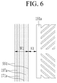
- the liquid crystal molecules may spread to the neighboring pixels through the separation region LA.
- the separation region LA is not provided in the first sub-spacer SS 1
- the liquid crystal molecules provided on the pixel electrode 191 may not flow to the neighboring pixels but remain between the first sub-spacer SS 1 and the second sub-spacer SS 2 .
- the liquid crystal molecules do not sufficiently flow but are gathered as described above, it may be seen as a defect.
Abstract
Description
Claims (20)
Applications Claiming Priority (2)
| Application Number | Priority Date | Filing Date | Title |
|---|---|---|---|
| KR10-2018-0143689 | 2018-11-20 | ||
| KR1020180143689A KR20200059362A (en) | 2018-11-20 | 2018-11-20 | Liquid crystal device |
Publications (2)
| Publication Number | Publication Date |
|---|---|
| US20200159057A1 US20200159057A1 (en) | 2020-05-21 |
| US11143919B2 true US11143919B2 (en) | 2021-10-12 |
Family
ID=70728214
Family Applications (1)
| Application Number | Title | Priority Date | Filing Date |
|---|---|---|---|
| US16/416,255 Active US11143919B2 (en) | 2018-11-20 | 2019-05-19 | Liquid crystal display including spacers |
Country Status (3)
| Country | Link |
|---|---|
| US (1) | US11143919B2 (en) |
| KR (1) | KR20200059362A (en) |
| CN (1) | CN111198461A (en) |
Families Citing this family (1)
| Publication number | Priority date | Publication date | Assignee | Title |
|---|---|---|---|---|
| CN212808869U (en) * | 2020-10-16 | 2021-03-26 | 北京京东方光电科技有限公司 | Liquid crystal display panel and electronic paper |
Citations (13)
| Publication number | Priority date | Publication date | Assignee | Title |
|---|---|---|---|---|
| JP2001311952A (en) | 2000-04-28 | 2001-11-09 | Fuji Xerox Co Ltd | Display element |
| KR20050061859A (en) | 2003-12-18 | 2005-06-23 | 엘지.필립스 엘시디 주식회사 | Liquid crystal display device |
| KR20110088215A (en) | 2010-01-28 | 2011-08-03 | 삼성모바일디스플레이주식회사 | Liquid crystal display |
| US20150036073A1 (en) * | 2013-08-02 | 2015-02-05 | Samsung Display Co., Ltd. | Liquid crystal display |
| KR20150031113A (en) | 2013-09-13 | 2015-03-23 | 삼성디스플레이 주식회사 | Liquid crystal display |
| US20150103296A1 (en) * | 2013-10-14 | 2015-04-16 | Samsung Display Co., Ltd. | Liquid crystal display |
| US20160013250A1 (en) * | 2014-07-09 | 2016-01-14 | Samsung Display Co., Ltd. | Display substrate and method of manufacturing the same |
| US20160187701A1 (en) * | 2014-06-24 | 2016-06-30 | Shenzen China Star Optoelectronics Technology Co., Ltd. | Support structure of display panel and display panel |
| US20160231617A1 (en) * | 2015-02-09 | 2016-08-11 | Samsung Display Co., Ltd. | Liquid crystal display and manufacturing method of the same |
| US20170192279A1 (en) * | 2016-01-05 | 2017-07-06 | Japan Display Inc. | Display device |
| KR20170125143A (en) | 2016-05-03 | 2017-11-14 | 삼성디스플레이 주식회사 | Liquid crystal display device |
| US20190033628A1 (en) * | 2017-07-26 | 2019-01-31 | Japan Display Inc. | Display device |
| US20190094596A1 (en) * | 2017-09-26 | 2019-03-28 | Wuhan China Star Optoelectronics Technology Co., Ltd. | Rgbx display panel and liquid crystal display device |
Family Cites Families (2)
| Publication number | Priority date | Publication date | Assignee | Title |
|---|---|---|---|---|
| KR102224348B1 (en) * | 2014-09-22 | 2021-03-09 | 엘지디스플레이 주식회사 | Liquid crystal display panel and method of manufacturing the same |
| KR102459604B1 (en) * | 2016-01-06 | 2022-10-31 | 삼성디스플레이 주식회사 | Display substrate and liquid crystal display comprising the same |
-
2018
- 2018-11-20 KR KR1020180143689A patent/KR20200059362A/en not_active Application Discontinuation
-
2019
- 2019-05-19 US US16/416,255 patent/US11143919B2/en active Active
- 2019-10-10 CN CN201910958043.3A patent/CN111198461A/en active Pending
Patent Citations (13)
| Publication number | Priority date | Publication date | Assignee | Title |
|---|---|---|---|---|
| JP2001311952A (en) | 2000-04-28 | 2001-11-09 | Fuji Xerox Co Ltd | Display element |
| KR20050061859A (en) | 2003-12-18 | 2005-06-23 | 엘지.필립스 엘시디 주식회사 | Liquid crystal display device |
| KR20110088215A (en) | 2010-01-28 | 2011-08-03 | 삼성모바일디스플레이주식회사 | Liquid crystal display |
| US20150036073A1 (en) * | 2013-08-02 | 2015-02-05 | Samsung Display Co., Ltd. | Liquid crystal display |
| KR20150031113A (en) | 2013-09-13 | 2015-03-23 | 삼성디스플레이 주식회사 | Liquid crystal display |
| US20150103296A1 (en) * | 2013-10-14 | 2015-04-16 | Samsung Display Co., Ltd. | Liquid crystal display |
| US20160187701A1 (en) * | 2014-06-24 | 2016-06-30 | Shenzen China Star Optoelectronics Technology Co., Ltd. | Support structure of display panel and display panel |
| US20160013250A1 (en) * | 2014-07-09 | 2016-01-14 | Samsung Display Co., Ltd. | Display substrate and method of manufacturing the same |
| US20160231617A1 (en) * | 2015-02-09 | 2016-08-11 | Samsung Display Co., Ltd. | Liquid crystal display and manufacturing method of the same |
| US20170192279A1 (en) * | 2016-01-05 | 2017-07-06 | Japan Display Inc. | Display device |
| KR20170125143A (en) | 2016-05-03 | 2017-11-14 | 삼성디스플레이 주식회사 | Liquid crystal display device |
| US20190033628A1 (en) * | 2017-07-26 | 2019-01-31 | Japan Display Inc. | Display device |
| US20190094596A1 (en) * | 2017-09-26 | 2019-03-28 | Wuhan China Star Optoelectronics Technology Co., Ltd. | Rgbx display panel and liquid crystal display device |
Also Published As
| Publication number | Publication date |
|---|---|
| CN111198461A (en) | 2020-05-26 |
| US20200159057A1 (en) | 2020-05-21 |
| KR20200059362A (en) | 2020-05-29 |
Similar Documents
| Publication | Publication Date | Title |
|---|---|---|
| US9910331B2 (en) | Display device | |
| TWI521272B (en) | Display panel | |
| CN107957644B (en) | Display device with rounded edges | |
| US20150092132A1 (en) | Thin film transistor array panel, liquid crystal display and manufacturing method of thin film transistor array panel | |
| TWI402587B (en) | Liquid crystal display device | |
| TWI581038B (en) | Liquid crystal display panel | |
| TWI753527B (en) | Display device | |
| US20180011377A1 (en) | Curved display device | |
| US10379405B2 (en) | Display device | |
| TW201445227A (en) | Liquid crystal display device | |
| TWI752954B (en) | Display apparatus and method of manufacturing the same | |
| US20160282690A1 (en) | Liquid crystal display device and related manufacturing method | |
| JP6220628B2 (en) | Display device | |
| US11143919B2 (en) | Liquid crystal display including spacers | |
| US9703152B2 (en) | Liquid crystal display device | |
| JP2016142943A (en) | Liquid crystal display device | |
| JP5143664B2 (en) | LCD panel | |
| US9785002B2 (en) | Liquid crystal display and method of manufacturing the same | |
| JP2009047729A (en) | Liquid crystal display panel | |
| KR102162755B1 (en) | Thin Film Transistor Substrate For High Resolution Liquid Crystal Display Having High Apperture Ratio and Manufacturing Method Thereof | |
| KR102016567B1 (en) | Flat panel display including thin film transistor substrate having color filter layer and manufacturing the same | |
| US20160195759A1 (en) | Liquid crystal display | |
| US20160209693A1 (en) | Display device | |
| TWI771244B (en) | Display device | |
| US20160306217A1 (en) | Display panels and blind including the same |
Legal Events
| Date | Code | Title | Description |
|---|---|---|---|
| FEPP | Fee payment procedure |
Free format text: ENTITY STATUS SET TO UNDISCOUNTED (ORIGINAL EVENT CODE: BIG.); ENTITY STATUS OF PATENT OWNER: LARGE ENTITY |
|
| STPP | Information on status: patent application and granting procedure in general |
Free format text: FINAL REJECTION MAILED |
|
| STPP | Information on status: patent application and granting procedure in general |
Free format text: RESPONSE AFTER FINAL ACTION FORWARDED TO EXAMINER |
|
| STPP | Information on status: patent application and granting procedure in general |
Free format text: ADVISORY ACTION MAILED |
|
| STPP | Information on status: patent application and granting procedure in general |
Free format text: DOCKETED NEW CASE - READY FOR EXAMINATION |
|
| STPP | Information on status: patent application and granting procedure in general |
Free format text: NON FINAL ACTION MAILED |
|
| STPP | Information on status: patent application and granting procedure in general |
Free format text: RESPONSE TO NON-FINAL OFFICE ACTION ENTERED AND FORWARDED TO EXAMINER |
|
| STPP | Information on status: patent application and granting procedure in general |
Free format text: NOTICE OF ALLOWANCE MAILED -- APPLICATION RECEIVED IN OFFICE OF PUBLICATIONS |
|
| STPP | Information on status: patent application and granting procedure in general |
Free format text: PUBLICATIONS -- ISSUE FEE PAYMENT RECEIVED |
|
| STPP | Information on status: patent application and granting procedure in general |
Free format text: PUBLICATIONS -- ISSUE FEE PAYMENT VERIFIED |
|
| STCF | Information on status: patent grant |
Free format text: PATENTED CASE |