US11139339B2 - Array substrate, method of manufacturing the same, and display device - Google Patents
Array substrate, method of manufacturing the same, and display device Download PDFInfo
- Publication number
- US11139339B2 US11139339B2 US16/461,419 US201816461419A US11139339B2 US 11139339 B2 US11139339 B2 US 11139339B2 US 201816461419 A US201816461419 A US 201816461419A US 11139339 B2 US11139339 B2 US 11139339B2
- Authority
- US
- United States
- Prior art keywords
- electrode
- light emitting
- thin film
- film transistor
- emitting diode
- Prior art date
- Legal status (The legal status is an assumption and is not a legal conclusion. Google has not performed a legal analysis and makes no representation as to the accuracy of the status listed.)
- Active, expires
Links
- 239000000758 substrate Substances 0.000 title claims abstract description 225
- 238000004519 manufacturing process Methods 0.000 title claims description 24
- 239000010409 thin film Substances 0.000 claims abstract description 166
- 239000010410 layer Substances 0.000 claims description 441
- 239000004065 semiconductor Substances 0.000 claims description 101
- 239000010408 film Substances 0.000 claims description 77
- 238000000034 method Methods 0.000 claims description 48
- 239000011229 interlayer Substances 0.000 claims description 34
- 239000000463 material Substances 0.000 claims description 28
- 239000011241 protective layer Substances 0.000 claims description 19
- TWNQGVIAIRXVLR-UHFFFAOYSA-N oxo(oxoalumanyloxy)alumane Chemical compound O=[Al]O[Al]=O TWNQGVIAIRXVLR-UHFFFAOYSA-N 0.000 claims description 10
- 239000011777 magnesium Substances 0.000 claims description 8
- RTAQQCXQSZGOHL-UHFFFAOYSA-N Titanium Chemical compound [Ti] RTAQQCXQSZGOHL-UHFFFAOYSA-N 0.000 claims description 7
- MRELNEQAGSRDBK-UHFFFAOYSA-N lanthanum(3+);oxygen(2-) Chemical compound [O-2].[O-2].[O-2].[La+3].[La+3] MRELNEQAGSRDBK-UHFFFAOYSA-N 0.000 claims description 7
- PLDDOISOJJCEMH-UHFFFAOYSA-N neodymium(3+);oxygen(2-) Chemical compound [O-2].[O-2].[O-2].[Nd+3].[Nd+3] PLDDOISOJJCEMH-UHFFFAOYSA-N 0.000 claims description 7
- ZIKATJAYWZUJPY-UHFFFAOYSA-N thulium(iii) oxide Chemical compound [O-2].[O-2].[O-2].[Tm+3].[Tm+3] ZIKATJAYWZUJPY-UHFFFAOYSA-N 0.000 claims description 7
- UQSXHKLRYXJYBZ-UHFFFAOYSA-N Iron oxide Chemical compound [Fe]=O UQSXHKLRYXJYBZ-UHFFFAOYSA-N 0.000 claims description 6
- FYYHWMGAXLPEAU-UHFFFAOYSA-N Magnesium Chemical compound [Mg] FYYHWMGAXLPEAU-UHFFFAOYSA-N 0.000 claims description 5
- DRVWBEJJZZTIGJ-UHFFFAOYSA-N cerium(3+);oxygen(2-) Chemical compound [O-2].[O-2].[O-2].[Ce+3].[Ce+3] DRVWBEJJZZTIGJ-UHFFFAOYSA-N 0.000 claims description 5
- 229910000421 cerium(III) oxide Inorganic materials 0.000 claims description 5
- 229910003440 dysprosium oxide Inorganic materials 0.000 claims description 5
- NLQFUUYNQFMIJW-UHFFFAOYSA-N dysprosium(iii) oxide Chemical compound O=[Dy]O[Dy]=O NLQFUUYNQFMIJW-UHFFFAOYSA-N 0.000 claims description 5
- 229910001940 europium oxide Inorganic materials 0.000 claims description 5
- AEBZCFFCDTZXHP-UHFFFAOYSA-N europium(3+);oxygen(2-) Chemical compound [O-2].[O-2].[O-2].[Eu+3].[Eu+3] AEBZCFFCDTZXHP-UHFFFAOYSA-N 0.000 claims description 5
- 229910003443 lutetium oxide Inorganic materials 0.000 claims description 5
- 229910052749 magnesium Inorganic materials 0.000 claims description 5
- 229910044991 metal oxide Inorganic materials 0.000 claims description 5
- 150000004706 metal oxides Chemical class 0.000 claims description 5
- MPARYNQUYZOBJM-UHFFFAOYSA-N oxo(oxolutetiooxy)lutetium Chemical compound O=[Lu]O[Lu]=O MPARYNQUYZOBJM-UHFFFAOYSA-N 0.000 claims description 5
- SIWVEOZUMHYXCS-UHFFFAOYSA-N oxo(oxoyttriooxy)yttrium Chemical compound O=[Y]O[Y]=O SIWVEOZUMHYXCS-UHFFFAOYSA-N 0.000 claims description 5
- HYXGAEYDKFCVMU-UHFFFAOYSA-N scandium oxide Chemical compound O=[Sc]O[Sc]=O HYXGAEYDKFCVMU-UHFFFAOYSA-N 0.000 claims description 5
- AJNVQOSZGJRYEI-UHFFFAOYSA-N digallium;oxygen(2-) Chemical compound [O-2].[O-2].[O-2].[Ga+3].[Ga+3] AJNVQOSZGJRYEI-UHFFFAOYSA-N 0.000 claims description 4
- -1 holimium oxide Chemical compound 0.000 claims description 4
- FKTOIHSPIPYAPE-UHFFFAOYSA-N samarium(iii) oxide Chemical compound [O-2].[O-2].[O-2].[Sm+3].[Sm+3] FKTOIHSPIPYAPE-UHFFFAOYSA-N 0.000 claims description 4
- CWYNVVGOOAEACU-UHFFFAOYSA-N Fe2+ Chemical compound [Fe+2] CWYNVVGOOAEACU-UHFFFAOYSA-N 0.000 claims description 3
- WGLPBDUCMAPZCE-UHFFFAOYSA-N Trioxochromium Chemical compound O=[Cr](=O)=O WGLPBDUCMAPZCE-UHFFFAOYSA-N 0.000 claims description 3
- 229910000423 chromium oxide Inorganic materials 0.000 claims description 3
- 229910001195 gallium oxide Inorganic materials 0.000 claims description 3
- DEIVNMVWRDMSMJ-UHFFFAOYSA-N hydrogen peroxide;oxotitanium Chemical compound OO.[Ti]=O DEIVNMVWRDMSMJ-UHFFFAOYSA-N 0.000 claims description 3
- 229910001954 samarium oxide Inorganic materials 0.000 claims description 3
- 229910003451 terbium oxide Inorganic materials 0.000 claims description 3
- SCRZPWWVSXWCMC-UHFFFAOYSA-N terbium(iii) oxide Chemical compound [O-2].[O-2].[O-2].[Tb+3].[Tb+3] SCRZPWWVSXWCMC-UHFFFAOYSA-N 0.000 claims description 3
- 229910001935 vanadium oxide Inorganic materials 0.000 claims description 3
- XHCLAFWTIXFWPH-UHFFFAOYSA-N [O-2].[O-2].[O-2].[O-2].[O-2].[V+5].[V+5] Chemical compound [O-2].[O-2].[O-2].[O-2].[O-2].[V+5].[V+5] XHCLAFWTIXFWPH-UHFFFAOYSA-N 0.000 claims description 2
- 229940075630 samarium oxide Drugs 0.000 claims description 2
- 230000008569 process Effects 0.000 description 31
- 229910021420 polycrystalline silicon Inorganic materials 0.000 description 28
- VYPSYNLAJGMNEJ-UHFFFAOYSA-N Silicium dioxide Chemical compound O=[Si]=O VYPSYNLAJGMNEJ-UHFFFAOYSA-N 0.000 description 27
- 229920005591 polysilicon Polymers 0.000 description 27
- 229910002601 GaN Inorganic materials 0.000 description 18
- JMASRVWKEDWRBT-UHFFFAOYSA-N Gallium nitride Chemical compound [Ga]#N JMASRVWKEDWRBT-UHFFFAOYSA-N 0.000 description 18
- 229910052751 metal Inorganic materials 0.000 description 15
- 239000002184 metal Substances 0.000 description 15
- 238000005498 polishing Methods 0.000 description 11
- 229910052814 silicon oxide Inorganic materials 0.000 description 11
- 150000001875 compounds Chemical class 0.000 description 10
- 239000007789 gas Substances 0.000 description 10
- IJGRMHOSHXDMSA-UHFFFAOYSA-N Atomic nitrogen Chemical compound N#N IJGRMHOSHXDMSA-UHFFFAOYSA-N 0.000 description 9
- 229910052581 Si3N4 Inorganic materials 0.000 description 9
- 229910004205 SiNX Inorganic materials 0.000 description 9
- HQVNEWCFYHHQES-UHFFFAOYSA-N silicon nitride Chemical compound N12[Si]34N5[Si]62N3[Si]51N64 HQVNEWCFYHHQES-UHFFFAOYSA-N 0.000 description 9
- 238000004544 sputter deposition Methods 0.000 description 9
- 238000000151 deposition Methods 0.000 description 8
- 239000000377 silicon dioxide Substances 0.000 description 8
- 239000000126 substance Substances 0.000 description 8
- 239000010936 titanium Substances 0.000 description 8
- 229910021417 amorphous silicon Inorganic materials 0.000 description 7
- 238000000623 plasma-assisted chemical vapour deposition Methods 0.000 description 7
- 229910052719 titanium Inorganic materials 0.000 description 7
- XCZXGTMEAKBVPV-UHFFFAOYSA-N trimethylgallium Chemical compound C[Ga](C)C XCZXGTMEAKBVPV-UHFFFAOYSA-N 0.000 description 7
- 238000002425 crystallisation Methods 0.000 description 6
- 230000008025 crystallization Effects 0.000 description 6
- 230000008021 deposition Effects 0.000 description 6
- 238000005530 etching Methods 0.000 description 6
- 150000002500 ions Chemical class 0.000 description 6
- 229910052750 molybdenum Inorganic materials 0.000 description 6
- 238000000059 patterning Methods 0.000 description 6
- 229910052782 aluminium Inorganic materials 0.000 description 5
- QVGXLLKOCUKJST-UHFFFAOYSA-N atomic oxygen Chemical compound [O] QVGXLLKOCUKJST-UHFFFAOYSA-N 0.000 description 5
- 239000010949 copper Substances 0.000 description 5
- 239000001301 oxygen Substances 0.000 description 5
- 229910052760 oxygen Inorganic materials 0.000 description 5
- 238000000206 photolithography Methods 0.000 description 5
- CSCPPACGZOOCGX-UHFFFAOYSA-N Acetone Chemical compound CC(C)=O CSCPPACGZOOCGX-UHFFFAOYSA-N 0.000 description 4
- QGZKDVFQNNGYKY-UHFFFAOYSA-N Ammonia Chemical compound N QGZKDVFQNNGYKY-UHFFFAOYSA-N 0.000 description 4
- JBRZTFJDHDCESZ-UHFFFAOYSA-N AsGa Chemical compound [As]#[Ga] JBRZTFJDHDCESZ-UHFFFAOYSA-N 0.000 description 4
- LFQSCWFLJHTTHZ-UHFFFAOYSA-N Ethanol Chemical compound CCO LFQSCWFLJHTTHZ-UHFFFAOYSA-N 0.000 description 4
- 230000008901 benefit Effects 0.000 description 4
- 238000006243 chemical reaction Methods 0.000 description 4
- 239000002131 composite material Substances 0.000 description 4
- 229910052802 copper Inorganic materials 0.000 description 4
- 239000007788 liquid Substances 0.000 description 4
- 238000001755 magnetron sputter deposition Methods 0.000 description 4
- 229910052757 nitrogen Inorganic materials 0.000 description 4
- 229920002120 photoresistant polymer Polymers 0.000 description 4
- GYHNNYVSQQEPJS-UHFFFAOYSA-N Gallium Chemical compound [Ga] GYHNNYVSQQEPJS-UHFFFAOYSA-N 0.000 description 3
- 229910001218 Gallium arsenide Inorganic materials 0.000 description 3
- GPXJNWSHGFTCBW-UHFFFAOYSA-N Indium phosphide Chemical compound [In]#P GPXJNWSHGFTCBW-UHFFFAOYSA-N 0.000 description 3
- 125000004429 atom Chemical group 0.000 description 3
- 239000008367 deionised water Substances 0.000 description 3
- 229910021641 deionized water Inorganic materials 0.000 description 3
- 229910052733 gallium Inorganic materials 0.000 description 3
- 239000011521 glass Substances 0.000 description 3
- 239000007769 metal material Substances 0.000 description 3
- 230000003647 oxidation Effects 0.000 description 3
- 238000007254 oxidation reaction Methods 0.000 description 3
- 235000012239 silicon dioxide Nutrition 0.000 description 3
- XLYOFNOQVPJJNP-UHFFFAOYSA-N water Chemical compound O XLYOFNOQVPJJNP-UHFFFAOYSA-N 0.000 description 3
- XKRFYHLGVUSROY-UHFFFAOYSA-N Argon Chemical compound [Ar] XKRFYHLGVUSROY-UHFFFAOYSA-N 0.000 description 2
- KZBUYRJDOAKODT-UHFFFAOYSA-N Chlorine Chemical compound ClCl KZBUYRJDOAKODT-UHFFFAOYSA-N 0.000 description 2
- 229910005451 FeTiO3 Inorganic materials 0.000 description 2
- KRHYYFGTRYWZRS-UHFFFAOYSA-N Fluorane Chemical compound F KRHYYFGTRYWZRS-UHFFFAOYSA-N 0.000 description 2
- 229910017676 MgTiO3 Inorganic materials 0.000 description 2
- 229910001257 Nb alloy Inorganic materials 0.000 description 2
- XLOMVQKBTHCTTD-UHFFFAOYSA-N Zinc monoxide Chemical compound [Zn]=O XLOMVQKBTHCTTD-UHFFFAOYSA-N 0.000 description 2
- 238000005229 chemical vapour deposition Methods 0.000 description 2
- 239000011651 chromium Substances 0.000 description 2
- 239000013078 crystal Substances 0.000 description 2
- 230000007547 defect Effects 0.000 description 2
- 238000010586 diagram Methods 0.000 description 2
- 238000000227 grinding Methods 0.000 description 2
- 229910021478 group 5 element Inorganic materials 0.000 description 2
- 238000010438 heat treatment Methods 0.000 description 2
- 239000001257 hydrogen Substances 0.000 description 2
- 229910052739 hydrogen Inorganic materials 0.000 description 2
- 238000002513 implantation Methods 0.000 description 2
- 239000012535 impurity Substances 0.000 description 2
- 238000011065 in-situ storage Methods 0.000 description 2
- 229910052738 indium Inorganic materials 0.000 description 2
- APFVFJFRJDLVQX-UHFFFAOYSA-N indium atom Chemical compound [In] APFVFJFRJDLVQX-UHFFFAOYSA-N 0.000 description 2
- 238000005468 ion implantation Methods 0.000 description 2
- JEIPFZHSYJVQDO-UHFFFAOYSA-N iron(III) oxide Inorganic materials O=[Fe]O[Fe]=O JEIPFZHSYJVQDO-UHFFFAOYSA-N 0.000 description 2
- 238000005224 laser annealing Methods 0.000 description 2
- 229910021421 monocrystalline silicon Inorganic materials 0.000 description 2
- 229910000069 nitrogen hydride Inorganic materials 0.000 description 2
- 239000002245 particle Substances 0.000 description 2
- 239000002243 precursor Substances 0.000 description 2
- 230000006798 recombination Effects 0.000 description 2
- 238000005215 recombination Methods 0.000 description 2
- 239000002356 single layer Substances 0.000 description 2
- FAQYAMRNWDIXMY-UHFFFAOYSA-N trichloroborane Chemical compound ClB(Cl)Cl FAQYAMRNWDIXMY-UHFFFAOYSA-N 0.000 description 2
- 238000004506 ultrasonic cleaning Methods 0.000 description 2
- 229910000980 Aluminium gallium arsenide Inorganic materials 0.000 description 1
- ZOXJGFHDIHLPTG-UHFFFAOYSA-N Boron Chemical compound [B] ZOXJGFHDIHLPTG-UHFFFAOYSA-N 0.000 description 1
- VYZAMTAEIAYCRO-UHFFFAOYSA-N Chromium Chemical compound [Cr] VYZAMTAEIAYCRO-UHFFFAOYSA-N 0.000 description 1
- RYGMFSIKBFXOCR-UHFFFAOYSA-N Copper Chemical compound [Cu] RYGMFSIKBFXOCR-UHFFFAOYSA-N 0.000 description 1
- UFHFLCQGNIYNRP-UHFFFAOYSA-N Hydrogen Chemical compound [H][H] UFHFLCQGNIYNRP-UHFFFAOYSA-N 0.000 description 1
- ZOKXTWBITQBERF-UHFFFAOYSA-N Molybdenum Chemical compound [Mo] ZOKXTWBITQBERF-UHFFFAOYSA-N 0.000 description 1
- XYFCBTPGUUZFHI-UHFFFAOYSA-N Phosphine Chemical compound P XYFCBTPGUUZFHI-UHFFFAOYSA-N 0.000 description 1
- OAICVXFJPJFONN-UHFFFAOYSA-N Phosphorus Chemical compound [P] OAICVXFJPJFONN-UHFFFAOYSA-N 0.000 description 1
- BLRPTPMANUNPDV-UHFFFAOYSA-N Silane Chemical compound [SiH4] BLRPTPMANUNPDV-UHFFFAOYSA-N 0.000 description 1
- XUIMIQQOPSSXEZ-UHFFFAOYSA-N Silicon Chemical compound [Si] XUIMIQQOPSSXEZ-UHFFFAOYSA-N 0.000 description 1
- 229910045601 alloy Inorganic materials 0.000 description 1
- 239000000956 alloy Substances 0.000 description 1
- XAGFODPZIPBFFR-UHFFFAOYSA-N aluminium Chemical compound [Al] XAGFODPZIPBFFR-UHFFFAOYSA-N 0.000 description 1
- PNEYBMLMFCGWSK-UHFFFAOYSA-N aluminium oxide Inorganic materials [O-2].[O-2].[O-2].[Al+3].[Al+3] PNEYBMLMFCGWSK-UHFFFAOYSA-N 0.000 description 1
- RNQKDQAVIXDKAG-UHFFFAOYSA-N aluminum gallium Chemical compound [Al].[Ga] RNQKDQAVIXDKAG-UHFFFAOYSA-N 0.000 description 1
- QNTVPKHKFIYODU-UHFFFAOYSA-N aluminum niobium Chemical compound [Al].[Nb] QNTVPKHKFIYODU-UHFFFAOYSA-N 0.000 description 1
- 229910021529 ammonia Inorganic materials 0.000 description 1
- 229910052787 antimony Inorganic materials 0.000 description 1
- WATWJIUSRGPENY-UHFFFAOYSA-N antimony atom Chemical compound [Sb] WATWJIUSRGPENY-UHFFFAOYSA-N 0.000 description 1
- 238000013459 approach Methods 0.000 description 1
- 229910052786 argon Inorganic materials 0.000 description 1
- 229910052785 arsenic Inorganic materials 0.000 description 1
- RQNWIZPPADIBDY-UHFFFAOYSA-N arsenic atom Chemical compound [As] RQNWIZPPADIBDY-UHFFFAOYSA-N 0.000 description 1
- 230000004888 barrier function Effects 0.000 description 1
- 230000015572 biosynthetic process Effects 0.000 description 1
- 229910052796 boron Inorganic materials 0.000 description 1
- 239000012159 carrier gas Substances 0.000 description 1
- 229910052804 chromium Inorganic materials 0.000 description 1
- 239000011248 coating agent Substances 0.000 description 1
- 238000000576 coating method Methods 0.000 description 1
- 239000000356 contaminant Substances 0.000 description 1
- 238000001816 cooling Methods 0.000 description 1
- 229910052593 corundum Inorganic materials 0.000 description 1
- 239000010431 corundum Substances 0.000 description 1
- 238000013461 design Methods 0.000 description 1
- ZOCHARZZJNPSEU-UHFFFAOYSA-N diboron Chemical compound B#B ZOCHARZZJNPSEU-UHFFFAOYSA-N 0.000 description 1
- BUMGIEFFCMBQDG-UHFFFAOYSA-N dichlorosilicon Chemical compound Cl[Si]Cl BUMGIEFFCMBQDG-UHFFFAOYSA-N 0.000 description 1
- QDOXWKRWXJOMAK-UHFFFAOYSA-N dichromium trioxide Chemical compound O=[Cr]O[Cr]=O QDOXWKRWXJOMAK-UHFFFAOYSA-N 0.000 description 1
- 238000009792 diffusion process Methods 0.000 description 1
- UBHZUDXTHNMNLD-UHFFFAOYSA-N dimethylsilane Chemical compound C[SiH2]C UBHZUDXTHNMNLD-UHFFFAOYSA-N 0.000 description 1
- PZPGRFITIJYNEJ-UHFFFAOYSA-N disilane Chemical compound [SiH3][SiH3] PZPGRFITIJYNEJ-UHFFFAOYSA-N 0.000 description 1
- 238000005516 engineering process Methods 0.000 description 1
- 238000004880 explosion Methods 0.000 description 1
- 229910021480 group 4 element Inorganic materials 0.000 description 1
- 125000004435 hydrogen atom Chemical class [H]* 0.000 description 1
- 230000001939 inductive effect Effects 0.000 description 1
- 229910010272 inorganic material Inorganic materials 0.000 description 1
- 239000011147 inorganic material Substances 0.000 description 1
- 238000004093 laser heating Methods 0.000 description 1
- 239000004973 liquid crystal related substance Substances 0.000 description 1
- 239000011159 matrix material Substances 0.000 description 1
- 238000005259 measurement Methods 0.000 description 1
- 229910021645 metal ion Inorganic materials 0.000 description 1
- 238000012986 modification Methods 0.000 description 1
- 230000004048 modification Effects 0.000 description 1
- 239000011733 molybdenum Substances 0.000 description 1
- DTSBBUTWIOVIBV-UHFFFAOYSA-N molybdenum niobium Chemical compound [Nb].[Mo] DTSBBUTWIOVIBV-UHFFFAOYSA-N 0.000 description 1
- 239000003921 oil Substances 0.000 description 1
- KFAFTZQGYMGWLU-UHFFFAOYSA-N oxo(oxovanadiooxy)vanadium Chemical compound O=[V]O[V]=O KFAFTZQGYMGWLU-UHFFFAOYSA-N 0.000 description 1
- 230000000737 periodic effect Effects 0.000 description 1
- 239000012071 phase Substances 0.000 description 1
- 229910052698 phosphorus Inorganic materials 0.000 description 1
- 239000011574 phosphorus Substances 0.000 description 1
- 238000007517 polishing process Methods 0.000 description 1
- 239000000047 product Substances 0.000 description 1
- 238000005086 pumping Methods 0.000 description 1
- 239000012495 reaction gas Substances 0.000 description 1
- 230000004044 response Effects 0.000 description 1
- 229910000077 silane Inorganic materials 0.000 description 1
- 229910052710 silicon Inorganic materials 0.000 description 1
- 239000010703 silicon Substances 0.000 description 1
- 239000012686 silicon precursor Substances 0.000 description 1
- 239000007790 solid phase Substances 0.000 description 1
- 238000005477 sputtering target Methods 0.000 description 1
- 238000006467 substitution reaction Methods 0.000 description 1
- 239000013589 supplement Substances 0.000 description 1
- 230000003746 surface roughness Effects 0.000 description 1
- 238000000427 thin-film deposition Methods 0.000 description 1
- 238000012546 transfer Methods 0.000 description 1
- 238000002834 transmittance Methods 0.000 description 1
- WFKWXMTUELFFGS-UHFFFAOYSA-N tungsten Chemical compound [W] WFKWXMTUELFFGS-UHFFFAOYSA-N 0.000 description 1
- 229910052721 tungsten Inorganic materials 0.000 description 1
- 239000010937 tungsten Substances 0.000 description 1
- 238000001771 vacuum deposition Methods 0.000 description 1
- 239000011787 zinc oxide Substances 0.000 description 1
Images


Classifications
-
- H01L27/156—
-
- H—ELECTRICITY
- H10—SEMICONDUCTOR DEVICES; ELECTRIC SOLID-STATE DEVICES NOT OTHERWISE PROVIDED FOR
- H10D—INORGANIC ELECTRIC SEMICONDUCTOR DEVICES
- H10D64/00—Electrodes of devices having potential barriers
- H10D64/60—Electrodes characterised by their materials
- H10D64/66—Electrodes having a conductor capacitively coupled to a semiconductor by an insulator, e.g. MIS electrodes
- H10D64/68—Electrodes having a conductor capacitively coupled to a semiconductor by an insulator, e.g. MIS electrodes characterised by the insulator, e.g. by the gate insulator
- H10D64/691—Electrodes having a conductor capacitively coupled to a semiconductor by an insulator, e.g. MIS electrodes characterised by the insulator, e.g. by the gate insulator comprising metallic compounds, e.g. metal oxides or metal silicates
-
- H—ELECTRICITY
- H10—SEMICONDUCTOR DEVICES; ELECTRIC SOLID-STATE DEVICES NOT OTHERWISE PROVIDED FOR
- H10D—INORGANIC ELECTRIC SEMICONDUCTOR DEVICES
- H10D86/00—Integrated devices formed in or on insulating or conducting substrates, e.g. formed in silicon-on-insulator [SOI] substrates or on stainless steel or glass substrates
- H10D86/01—Manufacture or treatment
-
- H01L29/4908—
-
- H01L29/517—
-
- H01L29/66757—
-
- H01L29/66765—
-
- H01L29/78675—
-
- H01L29/78678—
-
- H01L33/62—
-
- H—ELECTRICITY
- H10—SEMICONDUCTOR DEVICES; ELECTRIC SOLID-STATE DEVICES NOT OTHERWISE PROVIDED FOR
- H10D—INORGANIC ELECTRIC SEMICONDUCTOR DEVICES
- H10D30/00—Field-effect transistors [FET]
- H10D30/01—Manufacture or treatment
- H10D30/021—Manufacture or treatment of FETs having insulated gates [IGFET]
- H10D30/031—Manufacture or treatment of FETs having insulated gates [IGFET] of thin-film transistors [TFT]
- H10D30/0312—Manufacture or treatment of FETs having insulated gates [IGFET] of thin-film transistors [TFT] characterised by the gate electrodes
- H10D30/0314—Manufacture or treatment of FETs having insulated gates [IGFET] of thin-film transistors [TFT] characterised by the gate electrodes of lateral top-gate TFTs comprising only a single gate
-
- H—ELECTRICITY
- H10—SEMICONDUCTOR DEVICES; ELECTRIC SOLID-STATE DEVICES NOT OTHERWISE PROVIDED FOR
- H10D—INORGANIC ELECTRIC SEMICONDUCTOR DEVICES
- H10D30/00—Field-effect transistors [FET]
- H10D30/01—Manufacture or treatment
- H10D30/021—Manufacture or treatment of FETs having insulated gates [IGFET]
- H10D30/031—Manufacture or treatment of FETs having insulated gates [IGFET] of thin-film transistors [TFT]
- H10D30/0312—Manufacture or treatment of FETs having insulated gates [IGFET] of thin-film transistors [TFT] characterised by the gate electrodes
- H10D30/0316—Manufacture or treatment of FETs having insulated gates [IGFET] of thin-film transistors [TFT] characterised by the gate electrodes of lateral bottom-gate TFTs comprising only a single gate
-
- H—ELECTRICITY
- H10—SEMICONDUCTOR DEVICES; ELECTRIC SOLID-STATE DEVICES NOT OTHERWISE PROVIDED FOR
- H10D—INORGANIC ELECTRIC SEMICONDUCTOR DEVICES
- H10D30/00—Field-effect transistors [FET]
- H10D30/01—Manufacture or treatment
- H10D30/021—Manufacture or treatment of FETs having insulated gates [IGFET]
- H10D30/031—Manufacture or treatment of FETs having insulated gates [IGFET] of thin-film transistors [TFT]
- H10D30/0321—Manufacture or treatment of FETs having insulated gates [IGFET] of thin-film transistors [TFT] comprising silicon, e.g. amorphous silicon or polysilicon
-
- H—ELECTRICITY
- H10—SEMICONDUCTOR DEVICES; ELECTRIC SOLID-STATE DEVICES NOT OTHERWISE PROVIDED FOR
- H10D—INORGANIC ELECTRIC SEMICONDUCTOR DEVICES
- H10D30/00—Field-effect transistors [FET]
- H10D30/60—Insulated-gate field-effect transistors [IGFET]
- H10D30/67—Thin-film transistors [TFT]
- H10D30/6729—Thin-film transistors [TFT] characterised by the electrodes
- H10D30/673—Thin-film transistors [TFT] characterised by the electrodes characterised by the shapes, relative sizes or dispositions of the gate electrodes
- H10D30/6731—Top-gate only TFTs
-
- H—ELECTRICITY
- H10—SEMICONDUCTOR DEVICES; ELECTRIC SOLID-STATE DEVICES NOT OTHERWISE PROVIDED FOR
- H10D—INORGANIC ELECTRIC SEMICONDUCTOR DEVICES
- H10D30/00—Field-effect transistors [FET]
- H10D30/60—Insulated-gate field-effect transistors [IGFET]
- H10D30/67—Thin-film transistors [TFT]
- H10D30/6729—Thin-film transistors [TFT] characterised by the electrodes
- H10D30/673—Thin-film transistors [TFT] characterised by the electrodes characterised by the shapes, relative sizes or dispositions of the gate electrodes
- H10D30/6732—Bottom-gate only TFTs
-
- H—ELECTRICITY
- H10—SEMICONDUCTOR DEVICES; ELECTRIC SOLID-STATE DEVICES NOT OTHERWISE PROVIDED FOR
- H10D—INORGANIC ELECTRIC SEMICONDUCTOR DEVICES
- H10D30/00—Field-effect transistors [FET]
- H10D30/60—Insulated-gate field-effect transistors [IGFET]
- H10D30/67—Thin-film transistors [TFT]
- H10D30/6729—Thin-film transistors [TFT] characterised by the electrodes
- H10D30/6737—Thin-film transistors [TFT] characterised by the electrodes characterised by the electrode materials
- H10D30/6739—Conductor-insulator-semiconductor electrodes
-
- H—ELECTRICITY
- H10—SEMICONDUCTOR DEVICES; ELECTRIC SOLID-STATE DEVICES NOT OTHERWISE PROVIDED FOR
- H10D—INORGANIC ELECTRIC SEMICONDUCTOR DEVICES
- H10D30/00—Field-effect transistors [FET]
- H10D30/60—Insulated-gate field-effect transistors [IGFET]
- H10D30/67—Thin-film transistors [TFT]
- H10D30/674—Thin-film transistors [TFT] characterised by the active materials
- H10D30/6741—Group IV materials, e.g. germanium or silicon carbide
- H10D30/6743—Silicon
- H10D30/6745—Polycrystalline or microcrystalline silicon
-
- H—ELECTRICITY
- H10—SEMICONDUCTOR DEVICES; ELECTRIC SOLID-STATE DEVICES NOT OTHERWISE PROVIDED FOR
- H10H—INORGANIC LIGHT-EMITTING SEMICONDUCTOR DEVICES HAVING POTENTIAL BARRIERS
- H10H20/00—Individual inorganic light-emitting semiconductor devices having potential barriers, e.g. light-emitting diodes [LED]
- H10H20/80—Constructional details
- H10H20/85—Packages
- H10H20/857—Interconnections, e.g. lead-frames, bond wires or solder balls
-
- H—ELECTRICITY
- H10—SEMICONDUCTOR DEVICES; ELECTRIC SOLID-STATE DEVICES NOT OTHERWISE PROVIDED FOR
- H10H—INORGANIC LIGHT-EMITTING SEMICONDUCTOR DEVICES HAVING POTENTIAL BARRIERS
- H10H29/00—Integrated devices, or assemblies of multiple devices, comprising at least one light-emitting semiconductor element covered by group H10H20/00
- H10H29/10—Integrated devices comprising at least one light-emitting semiconductor component covered by group H10H20/00
- H10H29/14—Integrated devices comprising at least one light-emitting semiconductor component covered by group H10H20/00 comprising multiple light-emitting semiconductor components
- H10H29/142—Two-dimensional arrangements, e.g. asymmetric LED layout
-
- H01L2933/0066—
-
- H—ELECTRICITY
- H10—SEMICONDUCTOR DEVICES; ELECTRIC SOLID-STATE DEVICES NOT OTHERWISE PROVIDED FOR
- H10D—INORGANIC ELECTRIC SEMICONDUCTOR DEVICES
- H10D86/00—Integrated devices formed in or on insulating or conducting substrates, e.g. formed in silicon-on-insulator [SOI] substrates or on stainless steel or glass substrates
- H10D86/40—Integrated devices formed in or on insulating or conducting substrates, e.g. formed in silicon-on-insulator [SOI] substrates or on stainless steel or glass substrates characterised by multiple TFTs
- H10D86/60—Integrated devices formed in or on insulating or conducting substrates, e.g. formed in silicon-on-insulator [SOI] substrates or on stainless steel or glass substrates characterised by multiple TFTs wherein the TFTs are in active matrices
-
- H—ELECTRICITY
- H10—SEMICONDUCTOR DEVICES; ELECTRIC SOLID-STATE DEVICES NOT OTHERWISE PROVIDED FOR
- H10H—INORGANIC LIGHT-EMITTING SEMICONDUCTOR DEVICES HAVING POTENTIAL BARRIERS
- H10H20/00—Individual inorganic light-emitting semiconductor devices having potential barriers, e.g. light-emitting diodes [LED]
- H10H20/01—Manufacture or treatment
- H10H20/036—Manufacture or treatment of packages
- H10H20/0364—Manufacture or treatment of packages of interconnections
Definitions
- the present application relates to the field of display technologies, and in particular, to an array substrate, a method of manufacturing the array substrate, and a display device.
- a micro light-emitting diode is a light-emitting device using an inorganic material such as gallium nitride as a light-emitting material, and typically has a size in the range of, for example, 10 ⁇ m to 15 ⁇ m.
- the display device using the micro LED as the light-emitting device has the advantages such as high brightness, fast response, and high stability.
- thin film transistors are generally formed that are arranged in an array on a glass substrate, and a plurality of micro LEDs are formed on a separate monocrystalline silicon substrate. Then, the monocrystalline silicon substrate is diced to individual multiple micro LEDs. Finally, the individual micro LEDs are transferred to respective areas on the array substrate.
- an array substrate comprising: a base substrate; a thin film transistor disposed on the base substrate, the thin film transistor comprising a gate electrode connected to a gate line, an active layer, a gate insulating layer insulating the gate electrode from the active layer, a first electrode connected to a data line, and a second electrode spaced apart from the first electrode; a micro light emitting diode disposed on a side of the gate insulating layer away from the base substrate, the micro light emitting diode comprising a first electrode, a light emitting layer and a second electrode; and a common electrode.
- the second electrode of the thin film transistor is connected to one of the first and second electrodes of the micro light emitting diode.
- the other of the first and second electrodes of the micro light emitting diode is connected to the common electrode.
- the micro light emitting diode further comprises: a first semiconductor layer disposed on a side of the light emitting layer closer to the base substrate, and a second semiconductor layer disposed between the light emitting layer and the second electrode.
- the first semiconductor layer is in contact with the first electrode of the micro light emitting diode.
- the micro light emitting diode further comprises a buffer layer disposed between the first semiconductor layer and the gate insulating layer, and the buffer layer and the first electrode of the micro light emitting diode are located on the side of the gate insulating layer away from the base substrate.
- the gate insulating layer is made of a metal oxide material comprising at least one selected from a group consisting of aluminum oxide, iron oxide, chromium oxide, titanium trioxide, vanadium oxide, ferrous titanate, magnesium titanate, lanthanum oxide, cerous oxide, gallium oxide, scandium oxide, samarium oxide, europium oxide, terbium oxide, dysprosium oxide, yttrium oxide, holimium oxide, thulium oxide, lutetium oxide, and neodymium oxide.
- a metal oxide material comprising at least one selected from a group consisting of aluminum oxide, iron oxide, chromium oxide, titanium trioxide, vanadium oxide, ferrous titanate, magnesium titanate, lanthanum oxide, cerous oxide, gallium oxide, scandium oxide, samarium oxide, europium oxide, terbium oxide, dysprosium oxide, yttrium oxide, holimium oxide, thulium oxide, lutetium oxide, and
- the thin film transistor is of a structure selected from a group consisting of a top gate structure in which the gate electrode is in a same layer as and spaced apart from the first electrode of the micro light emitting diode, and a bottom gate structure in which the second electrode of the thin film transistor forms an integral structure with the first electrode of the micro light emitting diode or is connected to the second electrode of the micro light emitting diode.
- the thin film transistor is of the top gate structure.
- the array substrate further comprises an interlayer dielectric layer disposed on a side of the gate electrode away from the base substrate.
- the gate insulating layer is disposed on a side of the gate electrode closer to the base substrate.
- the active layer is disposed on a side of the gate insulating layer closer to the base substrate.
- the first and second electrodes of the thin film transistor are disposed on a side of the interlayer dielectric layer away from the base substrate, the first electrode of the thin film transistor is connected to the active layer through a first via disposed in the interlayer dielectric layer, and the second electrode of the thin film transistor is connected to the active layer through a second via disposed in the interlayer dielectric layer.
- the second electrode of the thin film transistor is connected to the first electrode of the micro light emitting diode through a first contact via disposed in the interlayer dielectric layer, and the second electrode of the micro light emitting diode is connected to the common electrode.
- the second electrode of the thin film transistor is in contact with the second electrode of the micro light emitting diode, and the first electrode of the micro light emitting diode is connected to the common electrode.
- the thin film transistor is of the bottom gate structure in which the second electrode of the thin film transistor forms the integral structure with the first electrode of the micro light emitting diode, one end of the integral structure is in contact with the active layer to form the second electrode of the thin film transistor, and the other end of the integral structure forms the first electrode of the micro light emitting diode.
- the thin film transistor is of the bottom gate structure in which the second electrode of the thin film transistor forms the integral structure with the first electrode of the micro light emitting diode.
- the array substrate further comprises a protective layer disposed on a side of the active layer away from the base substrate.
- the first electrode of the thin film transistor and the integral structure are disposed on a side of the protective layer away from the substrate.
- the first electrode of the thin film transistor is connected to the active layer through a third via disposed in the protective layer, one end of the integral structure is connected to the active layer through a fourth via disposed in the protective layer to form the second electrode of the thin film transistor, and the other end of the integral structure forms the first electrode of the micro light emitting diode.
- the common electrode is disposed in a same layer as the first electrode of the micro light emitting diode.
- the first electrode of the micro light emitting diode is spaced apart from the common electrode, the second electrode of the micro light emitting diode is in contact with a connection electrode, and the connection electrode is connected to the common electrode through a third contact via.
- the first electrode of the micro light emitting diode forms an integral structure with the common electrode.
- the common electrode is disposed on a side of the second electrode of the micro light emitting diode away from the base substrate, and the array substrate further comprises an insulating layer disposed between the common electrode and the second electrode.
- the common electrode is connected to the second electrode of the micro light emitting diode through a fourth contact via disposed in the insulating layer.
- the common electrode is connected to the first electrode of the micro light emitting diode through a fifth contact via extending through the insulating layer.
- a method of manufacturing an array substrate comprising: forming a thin film transistor on a base substrate, and a micro light emitting diode on a side of a gate insulating layer, away from the base substrate, of the thin film transistor, wherein the thin film transistor comprises a gate electrode connected to a gate line, an active layer, the gate insulating layer insulating the gate electrode from the active layer, a first electrode connected to a data line, and a second electrode spaced apart from the first electrode, and wherein the micro light emitting diode comprises a first electrode, a light emitting layer, and a second electrode; connecting the second electrode of the thin film transistor to one of the first and second electrodes of the micro light emitting diode; and connecting the other of the first and second electrodes of the micro light emitting diode to a common electrode.
- the forming the micro light emitting diode comprises: sequentially forming a first semiconductor layer, the light emitting layer, and a second semiconductor layer on a side of the gate insulating layer away from the substrate; forming the first electrode of the micro light emitting diode, which is in contact with the first semiconductor layer, on the side of the gate insulating layer away from the base substrate; and forming the second electrode of the micro light emitting diode on a side of the second semiconductor layer away from the base substrate.
- the method further comprises: forming a buffer layer on the side of the gate insulating layer away from the base substrate.
- the first semiconductor layer is formed on a side of the buffer layer away from the base substrate, and is in contact with the first electrode of the micro light emitting diode.
- the thin film transistor is of a top gate structure in which the gate electrode is in a same layer as and spaced apart from the first electrode of the micro light emitting diode.
- the forming the thin film transistor comprises: forming the active layer on the base substrate; forming the gate insulating layer on a side of the active layer away from the base substrate; forming the gate electrode on a side of the gate insulating layer away from the base substrate; forming an interlayer dielectric layer on a side of the gate electrode away from the base substrate; forming, on the base substrate, a first via and a second via extending through the interlayer dielectric layer and the gate insulating layer; and forming the first and second electrodes of the thin film transistor on a side of the interlayer dielectric layer away from the base substrate.
- the first electrode of the thin film transistor is connected to the active layer through the first via
- the second electrode of the thin film transistor is connected to the active layer through the second via.
- the method prior to the forming the first and second electrodes of the thin film transistor, the method further comprises forming a first contact via in the interlayer dielectric layer to expose the first electrode.
- the second electrode of the thin film transistor is connected to the first electrode of the micro light emitting diode through the first contact via, and the second electrode of the micro light emitting diode is connected to the common electrode.
- the thin film transistor is of a bottom gate structure in which the second electrode of the thin film transistor forms an integral structure with the first electrode of the micro light emitting diode.
- the forming the thin film transistor comprises: sequentially forming, on the base substrate, the gate electrode, the gate insulating layer, and the active layer of the thin film transistor; and forming the first electrode of the thin film transistor and the integral structure on the base substrate.
- One end of the integral structure is in contact with the active layer to form the second electrode of the thin film transistor, and the other end of the integral structure forms the first electrode of the micro light emitting diode.
- the thin film transistor is of a bottom gate structure in which the second electrode of the thin film transistor forms an integral structure with the first electrode of the micro light emitting diode.
- the forming the thin film transistor comprises: forming, on the base substrate, the gate electrode, the gate insulating layer and the active layer of the thin film transistor; forming a protective layer on a side of the active layer away from the base substrate; forming, in the protective layer, a third via and a fourth via for exposing the active layer, and a second contact via for exposing a first semiconductor layer of the micro light emitting diode; and forming the first electrode of the thin film transistor and the integrated structure on a side of the protective layer away from the base substrate.
- the first electrode of the thin film transistor is connected to the active layer through the third via, one end of the integral structure is connected to the active layer through the fourth via to form the second electrode of the thin film transistor, and the other end of the integrated structure is connected to the first semiconductor layer through the second contact via to form the first electrode of the micro light emitting diode.
- the forming the micro light emitting diode comprises forming the common electrode and the first electrode of the micro light emitting diode in a same layer by a one-time patterning process.
- the method further comprises: forming a third contact via to expose the common electrode; and forming a connection electrode which connects the second electrode of the micro light emitting diode to the common electrode through the third contact via.
- the method further comprises forming an insulating layer on a side of the second electrode of the micro light emitting diode away from the base substrate.
- the method further comprises: forming a fourth contact via in the insulating layer to expose the second electrode of the micro light emitting diode; and forming the common electrode on the insulating layer, wherein the common electrode is connected to the second electrode through the fourth contact via.
- the method further comprises: forming a fifth contact via to expose the first electrode; and forming the common electrode on the insulating layer, wherein the common electrode is connected to the first electrode through the fifth contact via.
- a display device comprising the array substrate as described above.
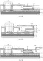
- FIG. 1 is a schematic cross-sectional view of a structure of an array substrate according to an embodiment of the present disclosure
- FIG. 2A is a schematic cross-sectional view of a structure of an array substrate according to another embodiment of the present disclosure
- FIG. 2B is a schematic cross-sectional view of a structure of an array substrate according to still another embodiment of the present disclosure
- FIG. 2C is a schematic plan view of the structure of the array substrate of FIG. 2A ;
- FIG. 3A is a schematic cross-sectional view of a structure of an array substrate according to still another embodiment of the present disclosure.
- FIG. 3B is a schematic cross-sectional view of a structure of an array substrate according to still another embodiment of the present disclosure.
- FIG. 3C is a schematic cross-sectional view of a structure of an array substrate according to still another embodiment of the present disclosure.
- FIG. 4A is a schematic cross-sectional view of a structure of an array substrate according to still another embodiment of the present disclosure.
- FIG. 4B is a schematic cross-sectional view of a structure of an array substrate according to still another embodiment of the present disclosure.
- FIG. 5A is a schematic cross-sectional view of a structure of an array substrate according to still another embodiment of the present disclosure.
- FIG. 5B is a schematic cross-sectional view of a structure of an array substrate according to still another embodiment of the present disclosure.
- FIG. 6 is a flow chart of a method of manufacturing an array substrate according to an embodiment of the present disclosure.
- FIG. 7A is a flowchart of a method of manufacturing an array substrate according to another embodiment of the present disclosure.
- FIG. 7B is a schematic cross-sectional view showing a structure obtained by forming an active layer on a base substrate
- FIG. 7C is a schematic view showing polishing of the active layer of FIG. 7B ;
- FIG. 7D is a schematic cross-sectional view showing a structure obtained by forming a gate insulating layer on the active layer of FIG. 7C ;
- FIG. 7E is a schematic cross-sectional view showing a structure obtained by forming a buffer layer, a first semiconductor layer, a light emitting layer, and a second semiconductor layer on the gate insulating layer of FIG. 7D ;
- FIG. 7F is a schematic cross-sectional view showing a structure obtained by removing a film layer, which is on the gate insulating layer and located in a non-pixel region, from the structure of FIG. 7E ;
- FIG. 7G is a schematic cross-sectional view showing a structure obtained by forming a gate electrode, a first electrode, and a second electrode on the structure of FIG. 7F ;
- FIG. 7H is a schematic cross-sectional view showing a structure obtained by forming vias in the structure of FIG. 7G ;
- FIG. 8A is a flow chart of a method of manufacturing a thin film transistor according to an embodiment of the present disclosure
- FIG. 8B is a flowchart of a method of manufacturing a thin film transistor according to another embodiment of the present disclosure.
- FIG. 9 is a schematic block diagram of a display device according to an embodiment of the present disclosure.
- first, second, third etc. may be used herein to describe various elements, components, regions, layers and/or sections, these elements, components, regions, layers and/or sections should not be limited by these terms. These terms are only used to distinguish one element, component, region, layer or section from another. Thus, a first element, component, region, layer or section discussed below could be termed a second element, component, region, layer or section without departing from the teachings of the present disclosure.
- spatially relative terms such as “beneath”, “below”, “lower”, “under”, “above”, “upper” and the like, may be used herein for ease of description to describe one element or feature's relationship to another element(s) or feature(s) as illustrated in the figures. It will be understood that the spatially relative terms are intended to encompass different orientations of the device in use or operation in addition to the orientation depicted in the figures. For example, if the device in the figures is turned over, elements described as “below” or “beneath” or “under” other elements or features would then be oriented “above” the other elements or features. Thus, the exemplary terms “below” and “under” can encompass both an orientation of above and below.
- Embodiments of the disclosure are described herein with reference to schematic illustrations of idealized embodiments (and intermediate structures) of the disclosure. As such, variations from the shapes of the illustrations as a result, for example, of manufacturing techniques and/or tolerances, are to be expected. Thus, embodiments of the disclosure should not be construed as limited to the particular shapes of regions illustrated herein but are to include deviations in shapes that result, for example, from manufacturing. Accordingly, the regions illustrated in the figures are schematic in nature and their shapes are not intended to illustrate the actual shape of a region of a device and are not intended to limit the scope of the disclosure.
- FIG. 1 is a schematic cross-sectional view of a structure of an array substrate according to an embodiment of the present disclosure.
- the array substrate may include a plurality of pixels arranged in an array, although only a single pixel is shown for convenience of illustration.
- the pixel includes a thin film transistor 10 disposed on a base substrate 00 .
- the thin film transistor 10 includes a gate electrode 12 connected to a gate line (not shown in FIG. 1 ), an active layer 15 , a gate insulating layer 11 that insulates the gate electrode from the active layer 15 , a first electrode 13 connected to a data line (not shown in FIG. 1 ), and a second electrode 14 spaced apart from the first electrode 13 .
- the pixel further includes a micro LED 20 disposed on a side of the gate insulating layer 11 away from the base substrate 00 .
- the micro LED 20 includes a first electrode 21 , a light emitting layer 22 , and a second electrode 23 .
- the second electrode 14 of the thin film transistor 10 is connected to the first electrode 21
- the second electrode 23 is connected to a common electrode (not shown in FIG. 1 ) configured to receive a common voltage.
- the second electrode 14 of the thin film transistor 10 may be connected to the second electrode 23
- the first electrode 21 may be connected to the common electrode.
- An electrode (the first electrode 21 in this example) of the micro LED 20 , which is connected to the second electrode 14 of the thin film transistor 10 , may be referred to as an anode, and an electrode (the second electrode 23 in this example) of the micro LED 20 , which is connected to the common electrode, may be referred to as a cathode.
- the thin film transistor 10 is used to drive the micro LED 20 to emit light.
- the first electrode 13 can be a source and the second electrode 14 can be a drain. Alternatively, the first electrode 13 can be a drain and the second electrode 14 can be a source.
- the first electrode 21 may be an N-type electrode, and the second electrode 23 may be a P-type electrode.
- the micro LEDs of the individual pixels may share an anode, i.e., the anodes of the micro LEDs of the individual pixels may be the same electrode.
- the light emitting layer 22 in the micro LED 20 may be formed of a material of a group III-V compound (including a binary compound, a ternary compound, or a quaternary compound, etc.).
- the group III-V compound refers to a compound formed of group III elements and group V elements in the periodic table of elements, with the group III elements including boron (B), aluminum (Al), gallium (Ga), indium (In), etc., and the group V elements including nitrogen (N), phosphorus (P), arsenic (As), antimony (Sb), etc.
- the group III-V compound generally includes gallium arsenide (GaAs), indium phosphide (InP), gallium nitride (GaN), etc.
- the semiconductor light emitting layer formed of the group III-V compound material has high luminous efficiency, good stability, and long life.
- the voltage applied to the common electrode of the array substrate may be different from the common electrode voltage of a conventional display device.
- the common electrode voltage in the conventional display device may be 0 volt (V), or near 0 V, for example, ⁇ 5 V to 5 V; whereas in the array substrate of the embodiment of the present disclosure, the voltage applied to the common electrode may not be limited to the above range.
- the cathode voltage applied to the common electrode ranges from ⁇ 20 V to 20 V, typically not equal to 0 V.
- FIG. 2A is a schematic cross-sectional view of a structure of an array substrate according to another embodiment of the present disclosure.
- the same elements as in FIG. 1 are denoted by the same reference signs and will not be described in detail herein.
- the micro LED 20 further includes a first semiconductor layer 24 disposed on a side of the light emitting layer 22 closer to the base substrate 00 , and a second semiconductor layer 25 disposed between the light emitting layer 22 and the second electrode 23 .
- the first electrode 21 is in contact with the first semiconductor layer 24 .
- the second semiconductor layer 25 in contact with the second electrode 23 (the cathode) may be an N-type semiconductor layer
- the first semiconductor layer 24 in contact with the first electrode 21 (the anode) may be a P-type semiconductor layer.
- the N-type semiconductor layer may be made of a group III-V compound material doped with a group IV element, for example, a GaN material doped with silicon (Si) atoms.
- the P-type semiconductor layer may be made of a group III-V compound material doped with a group II element, for example, a GaN material doped with magnesium (Mg) atoms.
- the micro LED 20 further includes a buffer layer 26 disposed between the first semiconductor layer 24 and the gate insulating layer 11 . Both the first electrode 21 and the buffer 26 layer are located on a side of the gate insulating layer 11 away from the base substrate 00 .
- the buffer layer 26 and the first semiconductor layer 24 have protrusions with respect to other film layers in the micro LED 20 , and the first electrode 21 covers the protrusion of the first semiconductor layer 24 , thereby achieving effective contact with the first semiconductor layer 24 .
- the gate insulating layer 11 may be made of a metal oxide material including any one of aluminum oxide (Al 2 O 3 ), iron oxide (Fe 2 O 3 ), chromium oxide (Cr 2 O 3 ), and titanium trioxide (Ti 2 O 3 ), vanadium oxide (V 2 O 3 ), ferrous titanate (FeTiO 3 ), magnesium titanate (MgTiO 3 ), lanthanum oxide (La 2 O 3 ), cerous oxide (Ce 2 O 3 ), gallium oxide (Ga 2 O 3 ), scandium oxide (Sc 2 O 3 )), samarium oxide (Sm 2 O 3 ), europium oxide (Eu 2 O 3 ), terbium oxide (Tb 2 O 3 ), dysprosium oxide (Dy 2 O 3 ), yttrium oxide (Y 2 O 3 ), holimium oxide (Ho 2 O 3 ), thulium oxide (Tm 2 O 3 ), lutetium oxide (Lu 2 O 3 ), aluminum oxide (
- a base buffer layer 01 may be disposed on the base substrate 00 . Both the thin film transistor 10 and the micro LED 20 are disposed on a side of the base buffer layer 01 away from the base substrate 00 .
- the base buffer layer 01 may be a composite film structure composed of a film of silicon nitride (SiN) and a film of silicon dioxide (SiO 2 ).
- FIG. 2B is a schematic cross-sectional view of a structure of an array substrate according to still another embodiment of the present disclosure.
- the same elements as in FIG. 2A are denoted by the same reference signs and will not be described in detail herein.
- the second electrode 14 of the thin film transistor 10 is in direct contact with the second electrode 23 of the micro LED 20 .
- a side of the second electrode 14 closer to the base substrate 00 is in contact with a side of the second electrode 23 away from the base substrate 00 .
- the first electrode 21 may be connected to a common electrode (not shown in FIG. 2B ).
- the thin film transistor 10 is of a top gate structure in which the gate insulating layer 11 is disposed on a side of the gate electrode 12 closer to the base substrate 00 , and the active layer 15 is disposed on a side of the gate insulating layer 11 closer to the base substrate 00 .
- the first electrode 21 of the micro LED 20 is disposed in the same layer as and spaced apart from the gate electrode 12 .
- an interlayer dielectric layer 03 is further disposed on a side of the gate electrode 12 away from the base substrate 00 , and the first electrode 13 and the second electrode 14 of the thin film transistor 10 are disposed, spatially spaced apart from each other, on a side of the interlayer dielectric layer 03 away from the base substrate 00 .
- FIG. 2C is a plan view of the structure shown in FIG. 2A .
- the first electrode 13 is connected to the active layer 15 through a first via V 1
- the second electrode 14 is connected to the active layer 15 through a second via V 2
- the second electrode 14 is connected to the first electrode 21 through a first contact via CV 1 .
- the first electrode 13 of the thin film transistor is connected to a data line 130
- the gate electrode 12 of the thin film transistor is connected to a gate line 120 , as can be seen from FIG. 2C .
- FIG. 3A is a schematic cross-sectional view of a structure of an array substrate according to still another embodiment of the present disclosure.
- the thin film transistor 10 is of a bottom gate structure, and the first electrode 21 of the micro LED 20 forms an integral structure with the second electrode 14 of the thin film transistor 10 .
- a portion of the integral structure that is in contact with the active region 15 forms the second electrode 14 of the thin film transistor 10
- a portion of the integral structure that is in contact with the first semiconductor layer 24 forms the first electrode 21 of the micro LED 20 .
- the second electrode 23 of the micro LED 20 is connected to a common electrode (not shown).
- the gate insulating layer 11 is disposed on a side of the gate electrode 12 away from the base substrate 00
- the active layer 15 is disposed on a side of the gate insulating layer 11 away from the base substrate 00
- the first electrode 13 of the thin film transistor 10 and the integral structure are disposed on a side of the gate insulating layer 11 away from the base substrate 00 and both are in contact with the active layer 15 .
- FIG. 3B is a schematic cross-sectional view of a structure of an array substrate according to still another embodiment of the present disclosure.
- the same elements as in FIG. 3A are denoted by the same reference signs and will not be described in detail herein.
- a protective layer 16 is further disposed on a side of the active layer 15 away from the base substrate 00 .
- the first electrode 13 of the thin film transistor 10 and the integral structure of the second electrode 14 and the first electrode 21 are disposed on a side of the protective layer 16 away from the base substrate 00 .
- the first electrode 13 is connected to the active layer 15 through a third via V 3 .
- One end of the integral structure is connected to the active layer 15 through the fourth via V 4 to form the second electrode 14 of the thin film transistor 10 .
- the other end of the integral structure is connected to the first semiconductor layer 24 through a second contact via CV 2 to form the first electrode 21 of the micro LED 20 .
- the first semiconductor layer 24 has a protrusion with respect to the light emitting layer 22 and the second semiconductor layer 25 , such that the integrated structure can be in contact with the protrusion of the first semiconductor layer 24 .
- FIG. 3C is a schematic cross-sectional view of a structure of an array substrate according to still another embodiment of the present disclosure.
- the same elements as in FIG. 3A are denoted by the same reference signs and will not be described in detail herein.
- the second electrode 14 of the thin film transistor 10 is in direct contact with the second electrode 23 of the micro LED 20 .
- a side of the second electrode 14 closer to the base substrate 00 is in contact with a side of the second electrode 23 away from the base substrate 00 .
- the first electrode 21 of the micro LED 20 may be connected to a common electrode (not shown).
- FIG. 4A is a schematic cross-sectional view of a structure of an array substrate according to still another embodiment of the present disclosure.
- the same elements as in FIG. 2A are denoted by the same reference signs and will not be described in detail herein.
- the common electrode 30 is disposed in the same layer as the first electrode 21 .
- the second electrode 14 of the thin film transistor 10 is connected to the first electrode 21 of the micro LED.
- a side of the second electrode 23 away from the base substrate 00 is further provided with a connection electrode 31 which is connected to a common electrode 30 through a third contact via CV 3 provided in a interlayer dielectric layer 03 .
- the connection electrode 31 is disposed in the same layer as the first electrode 13 and the second electrode 14 , and thus can be formed by a one-time patterning process.
- FIG. 4B is a schematic cross-sectional view of a structure of an array substrate according to still another embodiment of the present disclosure.
- the same elements as in FIG. 4A are denoted by the same reference signs and will not be described in detail herein.
- the second electrode 14 of the thin film transistor 10 is directly connected to the second electrode 23 of the micro LED, and the common electrode 30 forms an integral structure with the first electrode 21 of the micro LED.
- the integral structure is in direct contact with the first semiconductor layer 24 , and a portion of the integral structure that is in contact with the first semiconductor layer 24 forms the first electrode 21 of the micro LED 20 .
- FIG. 5A is a schematic cross-sectional view of a structure of an array substrate according to still another embodiment of the present disclosure.
- the same elements as in FIG. 2A are denoted by the same reference signs and will not be described in detail herein.
- the common electrode 30 is disposed on a side of the second electrode 23 away from the base substrate 00 , and an insulating layer 32 is formed between the common electrode 30 and the second electrode 23 .
- the second electrode 14 of the thin film transistor 10 is connected to the first electrode 21 of the micro LED 20
- the common electrode 30 is connected to the second electrode 23 of the micro LED 20 through a fourth contact via CV 4 provided in the insulating layer 32 .
- the active layer 15 in the thin film transistor 10 completely covers the base substrate.
- FIG. 5B is a schematic cross-sectional view of a structure of an array substrate according to still another embodiment of the present disclosure.
- the same elements as in FIG. 5A are denoted by the same reference signs and will not be described in detail herein.
- the common electrode 30 can be connected to the first electrode 21 through a fifth contact via CV 5 disposed in the insulating layer 32 and in the interlayer dielectric layer 03 .
- the active layer 15 is disposed only in the active region of the thin film transistor 10 .
- the micro LED can be formed simultaneously in the process of forming the thin film transistor, simplifying the manufacturing process of the array substrate and reducing the manufacturing cost of the display device.
- FIG. 6 is a flow chart of a method of manufacturing an array substrate according to an embodiment of the present disclosure. The method can be used to manufacture the array substrate shown in any of FIGS. 1 to 5B .
- a thin film transistor is formed on a base substrate, and a micro light emitting diode (LED) is formed on a side of a gate insulating layer, which is away from the base substrate, of the thin film transistor.
- the thin film transistor includes a gate electrode connected to a gate line, an active layer, the gate insulating layer that insulates the gate electrode from the active layer, a first electrode connected to a data line, and a second electrode spaced apart from the first electrode.
- the micro LED includes a first electrode, a light emitting layer, and a second electrode.
- the second electrode of the thin film transistor is connected to one of the first and second electrodes of the micro light emitting diode.
- the other of the first and second electrodes of the micro light emitting diode is connected to a common electrode. It will be understood that steps 101 through 103 may be an integral process although they are illustrated in FIG. 6 as being separate from each other.
- the manufacturing method provided by embodiments of the present disclosure consumes shorter process time and has higher yields as compared with conventional transfer processes.
- the process of forming the micro LED may include: sequentially forming a first semiconductor layer, a light emitting layer, and a second semiconductor layer on a side of the gate insulating layer away from the base substrate; and then forming a first electrode in contact with the first semiconductor layer on a side of the gate insulating layer away from the base substrate, and forming a second electrode on a side of the second semiconductor layer away from the base substrate.
- the manufacturing method may further include forming a buffer layer on a side of the gate insulating layer away from the base substrate before forming the first semiconductor layer.
- the first semiconductor layer may be formed on a side of the buffer layer away from the base substrate, and the first semiconductor layer may have a protrusion with respect to other film layers of the micro LED.
- the subsequently formed first electrode may overlie the protrusion of the first semiconductor layer to ensure effective contact with the first semiconductor layer.
- the method may include the following steps.
- a base buffer layer is formed on a base substrate.
- the base substrate may be a glass substrate.
- the base buffer layer may be a composite film structure composed of a film of silicon nitride (SiN) and a film of silicon dioxide (SiO 2 ).
- the base substrate when the base buffer layer is formed, the base substrate may be initially cleaned to remove impurity particles on the surface of the base substrate, and then the plasma enhanced chemical vapor deposition (PECVD) method is used to sequentially form a SiN film and a SiO 2 film on a surface of the base substrate, thereby obtaining the base buffer layer.
- the SiN film may have a thickness ranging from 50 nanometers (nm) to 100 nm, and the SiO2 film may have a thickness ranging from 100 nm to 400 nm.
- the SiN film has strong diffusion barrier property, and can inhibit the influence of metal ions in the glass substrate on the polysilicon film to be formed subsequently, and the SiO 2 film and the polysilicon film have an excellent interface, and can prevent the defects of the SiN film from damaging on the quality of the polysilicon film.
- an active layer is formed on a side of the base buffer layer away from the base substrate.
- the active layer may be formed on the surface of the base buffer layer using PECVD.
- the active layer may be formed of an amorphous silicon (a-Si) material, a polysilicon material, or indium gallium zinc oxide (IGZO).
- a layer of a-Si film having a thickness of 40 nm to 100 nm may be continuously deposited on the base buffer layer 01 by PECVD, and then the a-Si film may be dehydrogenated using a heat treatment furnace, in order to prevent hydrogen explosion during crystallization.
- An a-Si crystallization process can then be performed to form a polysilicon film.
- the a-Si film can usually be crystallized by laser annealing crystallization, metal induced crystallization or solid phase crystallization.
- the a-Si film may be subjected to laser annealing crystallization using a laser beam.
- the polysilicon film can be cleaned by using diluted hydrofluoric acid to reduce surface roughness of the polysilicon film and hence defects of the thin film transistor.
- ion implantation or ion cloud implantation may be used to perform channel doping of the thin film transistor on the polysilicon film to obtain the active layer.
- the doped ions in the channel doping are generally a mixed gas of phosphine (PH 3 ) and hydrogen (H 2 ), or a mixed gas of diborane (B 2 H 6 ) and H 2 .
- the dose for the ion implantation is between 10 11 and 10 13 ions/cm 2 (ions/cm 2 is the measurement unit of the negative ion concentration, which refers to the number of negative ions per square centimeter), and the implantation energy is between 10 and 100 kiloelectron volts (KeVs).
- the channel doping can effectively adjust the threshold voltage of the thin film transistor and improve the switching characteristics of the thin film transistor.
- a sacrificial layer may also be deposited on the surface of the polysilicon film.
- a layer of silicon nitride (SiN x ) may be deposited as the sacrificial layer.
- the sacrificial layer and the polysilicon film may be ground using a chemical mechanical polishing apparatus 40 having a grinding disc 41 and a polishing pad 42 .
- the grinding process may include two stages, wherein the first stage is for removing the sacrificial layer and the second stage is for simultaneously removing the polysilicon film and the residual sacrificial layer.
- the upper surface of the polysilicon film i.e., the side away from the base substrate 00
- the chemical mechanical polishing apparatus 40 is ground in this first stage, SiN x is continuously thinned, and part of the surface of the polysilicon film is exposed.
- the chemical mechanical polishing liquid may be an alkaline silica polishing liquid.
- a silicon oxide (SiO x ) film may be deposited on the surface of the polysilicon film as the sacrificial layer.
- the SiO x film may have a thickness of 800 to 120 angstroms, for example, 90 to 110 angstroms.
- the SiO x film may be formed on the surface of the polysilicon film by a dry oxidation process in which oxygen may be introduced into a reaction chamber to cause oxidation of the polysilicon to SiO x at a high temperature. The temperature and time of the oxidation can be adjusted where appropriate. This process is relatively mature and easy to design.
- the SiO x film can also be deposited by chemical vapor deposition.
- the SiO x film can be deposited by PECVD.
- the efficiency and cost control of the PECVD is relatively good.
- Those skilled in the art will appreciate that other well-known thin film deposition or epitaxial approaches can be used to form the SiO x film on the surface of the polysilicon film.
- the process of chemical mechanical polishing using a SiO x film as a sacrificial layer is similar to the process of chemical mechanical polishing using a SiN x film as a sacrificial layer, and the specific process thereof will not be described again.
- the surface of the polysilicon film may be wet-etched using an etching solution to remove residual sacrificial layer material on the surface of the polysilicon film, and residual particles generated by the chemical mechanical polishing process, thereby further reducing the roughness of the surface of the polysilicon film.
- a gate insulating layer is formed on a side of the active layer away from the base substrate.
- a metal oxide film may be formed on the surface of the active layer as the gate insulating layer by a magnetron sputtering process.
- a layer of Al 2 O 3 film may be formed as the gate insulating layer.
- the chemically and mechanically polished polycrystalline silicon film may be cleaned by ultrasonic cleaning using acetone, ethanol, and deionized water prior to coating. Then, in the ultrahigh vacuum magnetron sputtering system, an aluminum oxide film can be deposited on the surface of the polished active layer by radio frequency reactive magnetron sputtering, obtaining a gate insulating layer 11 as shown in FIG. 7D .
- high purity (of 99.998%) argon (Ar) can be used as a sputtering gas, and high purity (of 99.995%) oxygen (O 2 ) as a reaction gas.
- the sputtering target is high purity (of 99.99%) Al, and an oxide layer is present on the surface of the high purity Al target.
- pre-sputtering may be performed in pure Ar for 20 to 30 minutes to remove contaminants from the surface of the Al target.
- the sputtering parameters are a flow rate of 20 standard milliliters per minute (sccm) for the Ar gas, a working gas pressure of 2.0 Pascal (Pa), a sputtering power of 100 watts (W), and a temperature of 450 degrees Celsius for heating the base substrate.
- sccm standard milliliters per minute
- Pa working gas pressure
- W sputtering power
- W watts
- the background vacuum before sputtering should be higher than 5 ⁇ 10 ⁇ 5 Pa, wherein the background vacuum means that the gas in a certain space is vacuumized to a certain degree of vacuum using a vacuum pumping system in the vacuum coating.
- a sample baffle is turned away for formal sputtering.
- the sample is annealed in situ under an oxygen atmosphere in the vacuum chamber.
- the working atmosphere has a pressure of 0.5 Pa, which is advantageous for crystallizing the deposited film to form a hexagonal crystal structure (corundum).
- the aluminum oxide film can be better attached with the substrate (i.e., the active layer).
- the gate insulating layer may be formed of a metal oxide material, which may, in addition to Al 2 O 3 , be any of Fe 2 O 3 , Cr 2 O 3 , Ti 2 O 3 , V 2 O 3 , FeTiO 3 , MgTiO 3 , La 2 O 3 , Ce 2 O 3 , Ga 2 O 3 , Sc 2 O 3 , Sm 2 O 3 , Eu 2 O 3 , Tb 2 O 3 , Dy 2 O 3 , Y 2 O 3 , Ho 2 O 3 , Tm 2 O 3 , Lu 2 O 3 , and Nd 2 O 3 .
- a metal oxide material which may, in addition to Al 2 O 3 , be any of Fe 2 O 3 , Cr 2 O 3 , Ti 2 O 3 , V 2 O 3 , FeTiO 3 , MgTiO 3 , La 2 O 3 , Ce 2 O 3 , Ga 2 O 3 , Sc 2 O 3 , Sm 2 O 3 , Eu 2 O 3 , Tb
- a buffer layer is formed on a side of the gate insulating layer away from the base substrate.
- Metal organic chemical vapor deposition (MOCVD) may be used to deposit a GaN film on the surface of the gate insulating layer as the buffer layer, which buffer layer may improve the epitaxial lattice quality of the semiconductor layer to be formed subsequently.
- the base substrate on which the base buffer layer, the active layer and the gate insulating layer were formed may be rinsed for several times with absolute ethanol. Then, the base substrate is sequentially placed into acetone, absolute ethanol and deionized water for ultrasonic cleaning each for 10 minutes, then repeatedly rinsed with deionized water, and finally dried with high purity nitrogen (N 2 ).
- TMGa trimethylgallium
- low temperature deposition is performed on the base substrate on which the gate insulating layer was formed (the deposition temperature less than 500 degrees Celsius).
- the microwave source power fixed at 650 W, and the background vacuum better than 5.0 ⁇ 10-4 Pa
- a GaN low temperature buffer layer having a thickness of about 20 nm is first deposited in an environment of 300 degrees Celsius.
- the deposition conditions are flow rates of 0.4 sccm and 80 sccm respectively for TMGa and nitrogen, and a deposition time of 5 min.
- the temperature of the substrate is raised to 430 degrees Celsius, the flow rates of TMGa and nitrogen are 0.4 sccm and 80 sccm, respectively, and the deposition time is increased to 30 min.
- the buffer layer may be formed using a material such as GaAs or InP.
- a material such as GaAs or InP.
- the material alumina for forming the gate insulating layer has the same crystal structure as that of the materials such as GaAs and GaN.
- the lattice constant and thermal expansion coefficient do not match the III-V semiconductor material for epitaxial growth, its cost is low and the light transmittance is up to 90%, which is suitable for the laser heating process.
- a first semiconductor layer, a light emitting layer, and a second semiconductor layer are sequentially formed on a side of the buffer layer away from the base substrate.
- the first semiconductor layer may be an N-type semiconductor layer
- the second semiconductor layer may be a P-type semiconductor layer.
- a matrial such as InGaN, InAlGaP, GaP, GaAsP or AlGaAs can be selected to form the light emitting layer.
- the light emitting layer can also be referred to as a quantum well.
- a first semiconductor layer 24 , a light emitting layer 22 , and a second semiconductor layer 25 may be sequentially formed on the surface of a buffer layer 26 by an MOCVD process.
- the base substrate may be heated to a high temperature of about 600 degrees Celsius, and TMGa and an ammonia (NH 3 ) precursor are simultaneously introduced into a reaction chamber, thereby sequentially forming on the surface of the buffer layer 26 an N-type GaN semiconductor layer 24 , an InGaN or GaN quantum well 22 and a P-type GaN semiconductor layer 25 .
- the first semiconductor layer 24 and the second semiconductor layer 25 may be formed using an in-situ deposition state doping technique.
- the forming process may include adding a silicon precursor such as silane (SiH 4 ), disilane (Si 2 H 6 ), dimethylsilane (SiCH 8 ) or dichlorosilane (SiH 2 Cl 2 ) while introducing TMGa and NH 3 into the reaction chamber, so that the GaN is doped with Si of 10 17 to 10 20 cm ⁇ 3 (i.e., 10 17 to 10 20 Si atoms are doped per cubic centimeter of GaN), thereby depositing the N-type GaN semiconductor layer 24 .
- a silicon precursor such as silane (SiH 4 ), disilane (Si 2 H 6 ), dimethylsilane (SiCH 8 ) or dichlorosilane (SiH 2 Cl 2 )
- an organic precursor of magnesium such as magnesocene (Cp 2 Mg) is added to the reaction chamber so that Mg of 10 17 to 10 20 cm ⁇ 3 is doped in the GaN, thereby forming the P-type GaN semiconductor layer 25 .
- a wide bandgap material and a narrow bandgap semiconductor material each with a thickness in the order of nanometers, may be alternately deposited by an MOCVD process.
- a wide bandgap material aluminum gallium nitride (AlGaN) and a narrow bandgap material GaN are alternately deposited to form a variety of single quantum well or multiple quantum well structures.
- the wide bandgap material and the narrow bandgap material in the quantum well material have lattice constants and bands that match each other (the band difference of the two materials being kept within a certain range, for example, 1 eV), thereby being able to modulate the emission wavelength.
- the quantum well structure also has the advantages of high recombination efficiency and low interfacial recombination rate.
- the thickness of the buffer layer 26 may be between 0.1 and 5 micrometers
- the thickness of the first semiconductor layer 24 and the second semiconductor layer 25 may be between 0.1 and 0.5 micrometers
- the thickness of the quantum well 22 may be between 0.1 and 0.5 microns.
- the second semiconductor layer, the light emitting layer, the first semiconductor layer, and the buffer layer are removed from the non-pixel region.
- a one-time photolithography process may be employed to form a patterned photoresist mask on the surface of the base substrate to define pixel regions and non-pixel regions.
- the pixel region is an area for arranging the micro LED, that is, an effective display area of the array substrate.
- the non-pixel region is a non-display area.
- the pixel region may include a P region, a multiple quantum well (MQW) region, and an N region, of the micro LED, with the orthographic projections of the P region, the MQW region, and the N region onto the base substrate coinciding each other.
- MQW multiple quantum well
- portions of the second semiconductor layer, the light emitting layer, the first semiconductor layer, and the buffer layer that are not covered by the photoresist mask may be etched using an inductive coupled plasma emission spectrometer (ICP) etching machine.
- the etch depth may be 1.3 microns.
- the etching gas used in the ICP etching machine may be chlorine gas (Cl 2 ) and boron trichloride (BCl 3 ).
- the buffer layer 26 and the first semiconductor layer 24 may have protrusions with respect to other film layers in the micro LEDs 20 , which form an electrode contact region. It can also be seen with reference to FIG. 7F that the gate insulating layer 11 of the non-pixel region is exposed after the etching process.
- a gate electrode of the thin film transistor and a first electrode of the micro LED contacting the first semiconductor layer are formed on a side of the gate insulating layer away from the base substrate, and a second electrode of the micro LED is formed on a side of the second semiconductor layer away from the substrate.
- a metal thin film may be deposited on a surface of the gate insulating layer, and then the metal thin film may be processed by a one-time patterning process to form the gate electrode of the thin film transistor and the first electrode of the micro LED that are spaced apart from each other.
- the first electrode may overlie the protruding first semiconductor layer 24 to achieve effective contact with the first semiconductor layer 24 .
- a metal thin film having a thickness of 200 to 500 nm may be deposited on a surface of the base substrate by magnetron sputtering.
- the metal film may be a film layer formed of one of molybdenum (Mo), molybdenum-niobium alloy (MoNb), Al, aluminum-niobium alloy (AlNd), titanium (Ti), and copper (Cu), or may be a single or multiple layer composite laminate formed from multiple ones of the above materials.
- Mo film layer or an Al film layer may be formed on the surface of the base substrate, or a single-layer film or a multi-layer composite film composed of an alloy of Mo and Al may be formed.
- a patterned photoresist mask may be formed on the surface of the base substrate by a one-time photolithography process to define a gate region of the thin film transistor, and a first electrode region and a second electrode region of the micro LED.
- the region of the metal film not covered by the photoresist mask may be etched.
- the gate electrode 12 of the thin film transistor, and the first electrode 21 and the second electrode 23 of the micro LED may be obtained.
- the second electrode 23 is located on a side of the second semiconductor layer 25 away from the base substrate 00 , and the first electrode 21 overlies the protrusion of the first semiconductor layer 24 .
- an interlayer dielectric layer is formed on a side of the gate electrode away from the base substrate.
- the interlayer dielectric (ILD) layer may be formed on the side of the gate electrode away from the base substrate by a PECVD process.
- the interlayer dielectric layer may be a SiO x layer or a SiN x layer, or may be composed of a SiO x layer and a SiNx layer that are stacked.
- a first via and a second via are formed on the base substrate that extend through the interlayer dielectric layer and the gate insulating layer.
- the first via extending through the interlayer dielectric layer and the gate insulating layer can be formed in a source contact region on the base substrate
- the second via extending through the interlayer dielectric layer and the gate insulating layer can be formed in a drain contact region.
- a first via V 1 and a second via 32 may be formed on the base substrate, with the first via V 1 exposing the source contact region of the active layer 15 and the second via 32 exposing the drain contact region of the active layer 15 .
- the interlayer dielectric layer formed in the above step 1018 a may completely cover the surface of the base substrate, and that a portion of the interlayer dielectric layer overlying the second electrode 23 may be removed at the same time when the first via and the second via are formed by the one-time photolithography process in step 1019 a.
- a first electrode and a second electrode of the thin film transistor that are spaced apart from each other are formed on a side of the interlayer dielectric layer away from the base substrate.
- a metal thin film may be deposited on a surface of the interlayer dielectric layer, and then the metal thin film is patterned by a one-time photolithography process to form the first electrode and the second electrode of the thin film transistor.
- the first electrode is in contact with the source contact region in the active layer through the first via
- the second electrode is in contact with the drain contact region of the active layer through the second via.
- the metal thin film may be formed of any one of metal materials such as Cu, Al, Mo, Ti, chromium (Cr), or tungsten (W).
- the metal film may also be a multilayer metal film structure composed of a plurality of metal materials.
- the metal film may be a three-layer metal film, and the metal materials forming the three-layer metal film may be Mo, Al, and Mo, or Ti, Al, and Ti, or Ti, Cu, and Ti, or Mo, Cu, and Ti.
- the method may further include, before step 1020 a, forming a first contact via in the interlayer dielectric layer to expose the first electrode.
- the first contact via may be formed in synchronization with the first via and the second via.
- a first contact via 33 can be formed.
- the second electrode of the thin film transistor formed in the above step 1020 a may also be connected to the first electrode 21 through the first contact via 33 , and the second electrode 23 may be connected to the common electrode 30 .
- the structure of the finally formed array substrate can be seen with reference to FIG. 2A, 4A or 5A .
- a side of the second electrode, which is closer to the base substrate, of the thin film transistor formed in the above step 1020 a may be in contact with a side of the second electrode of the micro LED away from the base substrate. That is, the second electrode 14 of the thin film transistor is connected to the second electrode 23 of the micro LED, and the first electrode 21 of the micro LED is connected to the common electrode 30 .
- the structure of the finally formed array substrate can be seen with reference to FIG. 2B, 4B or 5B .
- the gate electrode and the first electrode may be formed first, and then the buffer layer, the first semiconductor layer, the light emitting layer, the second semiconductor layer, and the second electrode in the micro LED may be sequentially formed. That is, the operation of forming the gate electrode and the first electrode in the above step 1017 a may be performed before step 1014 a, the operation of forming the second electrode in the above step 1017 a may be performed after step 1016 a, and the above step 1016 a may be omitted.
- a method of manufacturing an array substrate of a thin film transistor having a bottom gate structure will be described below with reference to FIGS. 8A and 3A .
- a gate electrode 12 is formed on a base substrate 00 .
- a gate insulating layer 11 is formed on a side of the gate electrode 12 away from the base substrate 00 .
- a buffer layer 26 , a first semiconductor layer 24 , a light emitting layer 22 , and a second semiconductor layer 25 in the micro LED 20 are sequentially formed on a side of the gate insulating layer 11 away from the base substrate 00 .
- an active layer 15 is formed on a side of the gate insulating layer 11 away from the base substrate 00 .
- a first electrode 13 and an integral structure that are in contact with the active layer 15 are formed on a side of the gate insulating layer 11 away from the base substrate 00 , and a second electrode 23 is formed on a side of the second semiconductor layer 25 away from the base substrate 00 .
- One end of the integral structure that is in contact with the active layer 15 forms the second electrode 14 of the thin film transistor 10 , and the other end of the integral structure is in contact with the first semiconductor layer 24 of the micro LED 20 to form the first electrode 21 of the micro LED 20 .
- steps 1011 b to 1015 b may be performed according to the corresponding steps in the embodiment described above with reference to FIG. 7A , and are not described in detail herein again.
- a method of manufacturing an array substrate of a thin film transistor having a bottom gate structure will be described below with reference to FIGS. 8B and 3B .
- a gate electrode 12 is formed on a base substrate 00 .
- a gate insulating layer 11 is formed on a side of the gate electrode 12 away from the base substrate 00 .
- a buffer layer 26 , a first semiconductor layer 24 , a light emitting layer 22 , and a second semiconductor layer 25 in the micro LED 20 are sequentially formed on a side of the gate insulating layer 11 away from the base substrate 00 .
- an active layer 15 is formed on a side of the gate insulating layer 11 away from the base substrate 00 .
- a protective layer 16 is formed on a side of the active layer 15 away from the base substrate 00 .
- a third via V 3 and a fourth via V 4 for exposing the active layer 15 are formed in the protective layer 16 , and a second contact via CV 2 is formed for exposing the first semiconductor layer 24 .
- a first electrode 13 of the thin film transistor 10 and an integral structure are formed on a side of the protective layer 16 away from the base substrate 00 , and a second electrode 23 is formed on a side of the second semiconductor layer 25 away from the base substrate 00 .
- the first electrode 13 is connected to the active layer 15 through the third via V 3 .
- One end of the integral structure is connected to the active layer 15 through the fourth via V 4 to form the second electrode 14 of the thin film transistor 10
- the other end of the integrated structure is connected to the first semiconductor layer 24 through the second contact via CV 2 to form the first electrode 21 of the micro LED 20 .
- steps 1011 c to 1017 c may be performed according to the corresponding steps in the embodiment described above with reference to FIG. 7A , and are not described in detail herein again.
- the common electrode 30 and the first electrode 21 of the micro LED 20 may be formed in the same layer by a one-time patterning process.
- a third contact via CV 3 is formed to expose the common electrode 30 .
- the third contact via CV 3 may be formed while forming the first contact via CV 1 in the interlayer dielectric layer 03 .
- a connection electrode 31 is formed on a side of the second electrode 23 away from the base substrate 00 , and the connection electrode 31 is connected to the common electrode 30 through the third contact via CV 3 .
- the connection electrode 31 may be formed in the same layer as the first electrode 13 and the second electrode 14 of the thin film transistor 10 by a one-time patterning process.
- the common electrode 30 and the first electrode 21 of the micro LED 20 may be formed in the same layer by a one-time patterning process.
- the common electrode 30 and the first electrode 21 may be of an integral structure, that is, the common electrode 30 may be directly used as the first electrode 21 of the micro LED 20 .
- the common electrode 30 is formed on a side of the second electrode 23 of the micro LED 20 away from the base substrate 00 , and an insulating layer 32 is formed between the common electrode 30 and the second electrode 23 .
- a fourth contact via CV 4 is formed in the insulating layer 32 to expose the second electrode 23 .
- the common electrode 30 is connected to the second electrode 23 through the fourth contact via CV 4 .
- an insulating layer 32 is further formed on a side of the second electrode 23 away from the base substrate 00 .
- a fifth contact via CV 5 for exposing the first electrode 21 is formed in the insulating layer 32 and the interlayer dielectric layer 03 .
- the common electrode 30 is formed on a side of the insulating layer 32 away from the base substrate 00 , and is connected to the first electrode 21 through the fifth contact via CV 5 .
- FIG. 9 is a schematic block diagram of a display device according to an embodiment of the present disclosure.
- the display device may be any product or component having a display function such as a liquid crystal panel, an electronic paper, a mobile phone, a tablet computer, a television, a display, a notebook computer, a digital photo frame, a navigator, and the like.
- the display device includes a timing controller 910 , a scan driver 920 , a data driver 930 , and a display substrate 950 .
- the timing controller 910 receives synchronization signals and video signals R, and B from a system interface.
- the synchronization signals include a horizontal synchronization signal Hsync, a vertical synchronization signal Vsync, a main clock signal MCLK, and a data enable signal DE.
- the video signals R, G, and B contain luminance information of each of a plurality of pixels PX.
- the timing controller 910 generates a first driving control signal CONT 1 , a second driving control signal CONT 2 , and an image data signal DAT according to the video signals R, G, and B, the horizontal synchronization signal Hsync, the vertical synchronization signal Vsync, the data enable signal DE, and the main clock signal MCLK.
- the display substrate 950 includes the pixels PX arranged substantially in a matrix form.
- a plurality of substantially parallel scan lines S 1 to Sn extend in a row direction
- a plurality of substantially parallel data lines D 1 to Dm extend in a column direction.
- the scan lines S 1 to Sn and the data lines D 1 to Dm are connected to the pixels PX.
- the display substrate 950 can take the form of any of the array substrate embodiments described above with respect to FIGS. 1 through 5B .
- the scan driver 920 is connected to the scan lines S 1 -Sn, and generates corresponding scan signals S[ 1 ] to S[n] according to the first drive control signal CONT 1 .
- the scan driver 920 can sequentially apply the scan signals S[ 1 ] to S[n] to the scan lines S 1 to Sn.
- the data driver 930 is connected to the data lines D 1 to Dm, samples and holds the image data signal DAT according to the second driving control signal CONT 2 , and applies a plurality of data signals D[ 1 ] to D[m] to the data lines D 1 to Dm, respectively.
- the data driver 930 can program the data to the pixels PX by applying the data signals D[ 1 ] to D[m] to the data lines D 1 to Dm in synchronization with the scan signals S[ 1 ] to S[n].
Landscapes
- Devices For Indicating Variable Information By Combining Individual Elements (AREA)
- Thin Film Transistor (AREA)
- Electroluminescent Light Sources (AREA)
Abstract
Description
Claims (19)
Applications Claiming Priority (3)
| Application Number | Priority Date | Filing Date | Title |
|---|---|---|---|
| CN201810220239.8 | 2018-03-16 | ||
| CN201810220239.8A CN110277420B (en) | 2018-03-16 | 2018-03-16 | Array substrate, method for manufacturing the same, and display device |
| PCT/CN2018/115793 WO2019174290A1 (en) | 2018-03-16 | 2018-11-16 | Array substrate and manufacturing method therefor, and display device |
Publications (2)
| Publication Number | Publication Date |
|---|---|
| US20200258937A1 US20200258937A1 (en) | 2020-08-13 |
| US11139339B2 true US11139339B2 (en) | 2021-10-05 |
Family
ID=67908559
Family Applications (1)
| Application Number | Title | Priority Date | Filing Date |
|---|---|---|---|
| US16/461,419 Active 2039-04-08 US11139339B2 (en) | 2018-03-16 | 2018-11-16 | Array substrate, method of manufacturing the same, and display device |
Country Status (3)
| Country | Link |
|---|---|
| US (1) | US11139339B2 (en) |
| CN (1) | CN110277420B (en) |
| WO (1) | WO2019174290A1 (en) |
Cited By (1)
| Publication number | Priority date | Publication date | Assignee | Title |
|---|---|---|---|---|
| US20220415966A1 (en) * | 2021-06-28 | 2022-12-29 | Emagin Corporation | Monolithically Integrated Top-Gate Thin-Film Transistor and Light-Emitting Diode and Method of Making |
Families Citing this family (4)
| Publication number | Priority date | Publication date | Assignee | Title |
|---|---|---|---|---|
| DE102017111602A1 (en) * | 2017-05-29 | 2018-11-29 | Osram Opto Semiconductors Gmbh | Radiation-emitting component |
| CN116097440A (en) * | 2020-09-11 | 2023-05-09 | 华为技术有限公司 | Light-emitting panel, preparation method thereof and electronic equipment |
| CN112951845A (en) * | 2021-01-25 | 2021-06-11 | 武汉华星光电技术有限公司 | Array substrate |
| CN116344699A (en) * | 2021-12-16 | 2023-06-27 | 晶元光电股份有限公司 | Light-emitting element |
Citations (16)
| Publication number | Priority date | Publication date | Assignee | Title |
|---|---|---|---|---|
| CN101847646A (en) | 2010-02-02 | 2010-09-29 | 孙润光 | Inorganic light-emitting diode display device |
| US20120009710A1 (en) * | 2010-07-07 | 2012-01-12 | Young-Il Kim | Method of forming ldd of tft, method of fabricating tft and organic light emitting device using the method |
| US20120313076A1 (en) | 2011-06-10 | 2012-12-13 | The Regents Of The University Of California | Low droop light emitting diode structure on gallium nitride semipolar substrates |
| US20130313076A1 (en) | 2010-09-10 | 2013-11-28 | Johannes Stelter | Device for loading goods into and/or unloading goods from a loading space, particularly a container |
| CN104112755A (en) | 2013-04-16 | 2014-10-22 | 鸿富锦精密工业(深圳)有限公司 | Flip chip solid-state light-emitting display |
| WO2016051992A1 (en) | 2014-10-03 | 2016-04-07 | 株式会社ジャパンディスプレイ | Image display device |
| US20160336374A1 (en) * | 2015-05-15 | 2016-11-17 | Boe Technology Group Co., Ltd. | Display substrate, its manufacturing method and display device |
| WO2016200882A1 (en) * | 2015-06-08 | 2016-12-15 | Corning Incorporated | Microled display without transfer |
| CN106816512A (en) | 2017-03-03 | 2017-06-09 | 京东方科技集团股份有限公司 | A kind of diode displaying substrate and preparation method thereof, display |
| US20170179092A1 (en) | 2014-10-31 | 2017-06-22 | eLux Inc. | Hybrid Display using Inorganic Micro Light Emitting Diodes (uLEDs) and Organic LEDs (OLEDs) |
| US20170186828A1 (en) * | 2014-12-31 | 2017-06-29 | Boe Technology Group Co., Ltd. | Oled array substrate, manufacturing method thereof, and display apparatus |
| US20170294451A1 (en) * | 2016-04-12 | 2017-10-12 | Samsung Display Co., Ltd. | Display device |
| CN107742636A (en) | 2017-10-25 | 2018-02-27 | 上海天马微电子有限公司 | Display panel and display device |
| US20180122836A1 (en) * | 2016-10-28 | 2018-05-03 | Lg Display Co., Ltd. | Light emitting diode display device |
| US20180130910A1 (en) * | 2016-11-10 | 2018-05-10 | Joled Inc. | Thin-film transistor substrate |
| US20190074324A1 (en) * | 2017-09-05 | 2019-03-07 | Samsung Electronics Co., Ltd. | Display device including light emitting diode and method of manufacturing the same |
-
2018
- 2018-03-16 CN CN201810220239.8A patent/CN110277420B/en active Active
- 2018-11-16 US US16/461,419 patent/US11139339B2/en active Active
- 2018-11-16 WO PCT/CN2018/115793 patent/WO2019174290A1/en not_active Ceased
Patent Citations (18)
| Publication number | Priority date | Publication date | Assignee | Title |
|---|---|---|---|---|
| CN101847646A (en) | 2010-02-02 | 2010-09-29 | 孙润光 | Inorganic light-emitting diode display device |
| US20120009710A1 (en) * | 2010-07-07 | 2012-01-12 | Young-Il Kim | Method of forming ldd of tft, method of fabricating tft and organic light emitting device using the method |
| US20130313076A1 (en) | 2010-09-10 | 2013-11-28 | Johannes Stelter | Device for loading goods into and/or unloading goods from a loading space, particularly a container |
| US20120313076A1 (en) | 2011-06-10 | 2012-12-13 | The Regents Of The University Of California | Low droop light emitting diode structure on gallium nitride semipolar substrates |
| CN104112755A (en) | 2013-04-16 | 2014-10-22 | 鸿富锦精密工业(深圳)有限公司 | Flip chip solid-state light-emitting display |
| US20170278894A1 (en) | 2014-10-03 | 2017-09-28 | Japan Display Inc. | Image display device |
| WO2016051992A1 (en) | 2014-10-03 | 2016-04-07 | 株式会社ジャパンディスプレイ | Image display device |
| US20170179092A1 (en) | 2014-10-31 | 2017-06-22 | eLux Inc. | Hybrid Display using Inorganic Micro Light Emitting Diodes (uLEDs) and Organic LEDs (OLEDs) |
| US20170186828A1 (en) * | 2014-12-31 | 2017-06-29 | Boe Technology Group Co., Ltd. | Oled array substrate, manufacturing method thereof, and display apparatus |
| US20160336374A1 (en) * | 2015-05-15 | 2016-11-17 | Boe Technology Group Co., Ltd. | Display substrate, its manufacturing method and display device |
| WO2016200882A1 (en) * | 2015-06-08 | 2016-12-15 | Corning Incorporated | Microled display without transfer |
| US20170294451A1 (en) * | 2016-04-12 | 2017-10-12 | Samsung Display Co., Ltd. | Display device |
| US20180122836A1 (en) * | 2016-10-28 | 2018-05-03 | Lg Display Co., Ltd. | Light emitting diode display device |
| US10090335B2 (en) * | 2016-10-28 | 2018-10-02 | Lg Display Co., Ltd. | Light emitting diode display device |
| US20180130910A1 (en) * | 2016-11-10 | 2018-05-10 | Joled Inc. | Thin-film transistor substrate |
| CN106816512A (en) | 2017-03-03 | 2017-06-09 | 京东方科技集团股份有限公司 | A kind of diode displaying substrate and preparation method thereof, display |
| US20190074324A1 (en) * | 2017-09-05 | 2019-03-07 | Samsung Electronics Co., Ltd. | Display device including light emitting diode and method of manufacturing the same |
| CN107742636A (en) | 2017-10-25 | 2018-02-27 | 上海天马微电子有限公司 | Display panel and display device |
Non-Patent Citations (2)
| Title |
|---|
| Office action from Chinese Application No. 201810220239.8 dated Jan. 6, 2021. |
| Search Report and Written Opinion for International Application No. PCT/CN2018/115793 dated Feb. 21, 2019. |
Cited By (2)
| Publication number | Priority date | Publication date | Assignee | Title |
|---|---|---|---|---|
| US20220415966A1 (en) * | 2021-06-28 | 2022-12-29 | Emagin Corporation | Monolithically Integrated Top-Gate Thin-Film Transistor and Light-Emitting Diode and Method of Making |
| US12414424B2 (en) * | 2021-06-28 | 2025-09-09 | Emagin Corporation | Monolithically integrated top-gate thin-film transistor and light-emitting diode and method of making |
Also Published As
| Publication number | Publication date |
|---|---|
| WO2019174290A1 (en) | 2019-09-19 |
| CN110277420A (en) | 2019-09-24 |
| US20200258937A1 (en) | 2020-08-13 |
| CN110277420B (en) | 2021-11-02 |
Similar Documents
| Publication | Publication Date | Title |
|---|---|---|
| US11251223B2 (en) | Array substrate, method of manufacturing the same, and display device | |
| US11139339B2 (en) | Array substrate, method of manufacturing the same, and display device | |
| KR102649237B1 (en) | light emitting diode device | |
| CN108878468B (en) | Display substrate, manufacturing method thereof, display panel and display device | |
| US20220059726A1 (en) | Active matrix led array | |
| WO2022191998A1 (en) | Indium-gallium-nitride light emitting diodes with light reflecting mirrors | |
| US12490570B2 (en) | Thin-film LED array with low refractive index patterned structures | |
| CN102437170B (en) | Blue-light-excited TFT (thin film transistor)-LED (light emitting diode) array display substrate and manufacturing method thereof | |
| US20230155070A1 (en) | Thin-film led array with low refractive index patterned structures and reflector | |
| US12068357B2 (en) | Light emitting diode and preparation method therefor | |
| CN116093233A (en) | High-reliability thin-film flip-chip Micro-LED display chip and preparation method thereof | |
| CN114188458B (en) | Manufacturing method of light-emitting diode and light-emitting diode | |
| CN109801973B (en) | Thin film transistor and its manufacturing method, array substrate and display device | |
| CN202332854U (en) | TFT(thin film transistor)-LED(light-emitting diode) color array display substrate | |
| WO2021043745A1 (en) | Light emitting diode and method of forming a light emitting diode | |
| US11837683B2 (en) | Indium-gallium-nitride light emitting diodes with increased red-light quantum efficiency | |
| US12040432B2 (en) | Light emitting diode devices with patterned TCO layer including different thicknesses | |
| CN201667344U (en) | Gallium nitride series light emitting diode structure | |
| CN202363462U (en) | Blue-light excitation TFT-LED array display substrate | |
| TW202030880A (en) | Method for forming micro led display without performing mass transfer process | |
| CN113809213A (en) | Reduced voltage light-emitting diode chip and method of making the same | |
| JP2011124504A (en) | Method of manufacturing semiconductor light-emitting element |
Legal Events
| Date | Code | Title | Description |
|---|---|---|---|
| FEPP | Fee payment procedure |
Free format text: ENTITY STATUS SET TO UNDISCOUNTED (ORIGINAL EVENT CODE: BIG.); ENTITY STATUS OF PATENT OWNER: LARGE ENTITY |
|
| STPP | Information on status: patent application and granting procedure in general |
Free format text: NON FINAL ACTION MAILED |
|
| STPP | Information on status: patent application and granting procedure in general |
Free format text: RESPONSE TO NON-FINAL OFFICE ACTION ENTERED AND FORWARDED TO EXAMINER |
|
| STPP | Information on status: patent application and granting procedure in general |
Free format text: FINAL REJECTION MAILED |
|
| STPP | Information on status: patent application and granting procedure in general |
Free format text: DOCKETED NEW CASE - READY FOR EXAMINATION |
|
| STPP | Information on status: patent application and granting procedure in general |
Free format text: NOTICE OF ALLOWANCE MAILED -- APPLICATION RECEIVED IN OFFICE OF PUBLICATIONS |
|
| STPP | Information on status: patent application and granting procedure in general |
Free format text: PUBLICATIONS -- ISSUE FEE PAYMENT VERIFIED |
|
| STCF | Information on status: patent grant |
Free format text: PATENTED CASE |
|
| AS | Assignment |
Owner name: BEIJING BOE TECHNOLOGY DEVELOPMENT CO., LTD., CHINA Free format text: ASSIGNMENT OF ASSIGNORS INTEREST;ASSIGNOR:BOE TECHNOLOGY GROUP CO., LTD.;REEL/FRAME:060826/0252 Effective date: 20220726 |
|
| MAFP | Maintenance fee payment |
Free format text: PAYMENT OF MAINTENANCE FEE, 4TH YEAR, LARGE ENTITY (ORIGINAL EVENT CODE: M1551); ENTITY STATUS OF PATENT OWNER: LARGE ENTITY Year of fee payment: 4 |