US11127902B2 - Organic light-emitting display apparatus and method of manufacturing the same - Google Patents

Organic light-emitting display apparatus and method of manufacturing the same Download PDF

Info

Publication number
US11127902B2
US11127902B2 US16/549,413 US201916549413A US11127902B2 US 11127902 B2 US11127902 B2 US 11127902B2 US 201916549413 A US201916549413 A US 201916549413A US 11127902 B2 US11127902 B2 US 11127902B2
Authority
US
United States
Prior art keywords
layer
lift
photoresist
organic functional
functional layer
Prior art date
Legal status (The legal status is an assumption and is not a legal conclusion. Google has not performed a legal analysis and makes no representation as to the accuracy of the status listed.)
Active
Application number
US16/549,413
Other versions
US20190378986A1 (en
Inventor
Arong Kim
Jungsun PARK
Hyunsung BANG
Duckjung Lee
Jiyoung Choung
Current Assignee (The listed assignees may be inaccurate. Google has not performed a legal analysis and makes no representation or warranty as to the accuracy of the list.)
Samsung Display Co Ltd
Original Assignee
Samsung Display Co Ltd
Priority date (The priority date is an assumption and is not a legal conclusion. Google has not performed a legal analysis and makes no representation as to the accuracy of the date listed.)
Filing date
Publication date
Application filed by Samsung Display Co Ltd filed Critical Samsung Display Co Ltd
Priority to US16/549,413 priority Critical patent/US11127902B2/en
Publication of US20190378986A1 publication Critical patent/US20190378986A1/en
Application granted granted Critical
Publication of US11127902B2 publication Critical patent/US11127902B2/en
Active legal-status Critical Current
Anticipated expiration legal-status Critical

Links

Images

Classifications

    • HELECTRICITY
    • H10SEMICONDUCTOR DEVICES; ELECTRIC SOLID-STATE DEVICES NOT OTHERWISE PROVIDED FOR
    • H10KORGANIC ELECTRIC SOLID-STATE DEVICES
    • H10K71/00Manufacture or treatment specially adapted for the organic devices covered by this subclass
    • H01L51/0016
    • GPHYSICS
    • G03PHOTOGRAPHY; CINEMATOGRAPHY; ANALOGOUS TECHNIQUES USING WAVES OTHER THAN OPTICAL WAVES; ELECTROGRAPHY; HOLOGRAPHY
    • G03FPHOTOMECHANICAL PRODUCTION OF TEXTURED OR PATTERNED SURFACES, e.g. FOR PRINTING, FOR PROCESSING OF SEMICONDUCTOR DEVICES; MATERIALS THEREFOR; ORIGINALS THEREFOR; APPARATUS SPECIALLY ADAPTED THEREFOR
    • G03F7/00Photomechanical, e.g. photolithographic, production of textured or patterned surfaces, e.g. printing surfaces; Materials therefor, e.g. comprising photoresists; Apparatus specially adapted therefor
    • G03F7/004Photosensitive materials
    • G03F7/09Photosensitive materials characterised by structural details, e.g. supports, auxiliary layers
    • G03F7/094Multilayer resist systems, e.g. planarising layers
    • GPHYSICS
    • G03PHOTOGRAPHY; CINEMATOGRAPHY; ANALOGOUS TECHNIQUES USING WAVES OTHER THAN OPTICAL WAVES; ELECTROGRAPHY; HOLOGRAPHY
    • G03FPHOTOMECHANICAL PRODUCTION OF TEXTURED OR PATTERNED SURFACES, e.g. FOR PRINTING, FOR PROCESSING OF SEMICONDUCTOR DEVICES; MATERIALS THEREFOR; ORIGINALS THEREFOR; APPARATUS SPECIALLY ADAPTED THEREFOR
    • G03F7/00Photomechanical, e.g. photolithographic, production of textured or patterned surfaces, e.g. printing surfaces; Materials therefor, e.g. comprising photoresists; Apparatus specially adapted therefor
    • G03F7/004Photosensitive materials
    • G03F7/09Photosensitive materials characterised by structural details, e.g. supports, auxiliary layers
    • G03F7/095Photosensitive materials characterised by structural details, e.g. supports, auxiliary layers having more than one photosensitive layer
    • GPHYSICS
    • G03PHOTOGRAPHY; CINEMATOGRAPHY; ANALOGOUS TECHNIQUES USING WAVES OTHER THAN OPTICAL WAVES; ELECTROGRAPHY; HOLOGRAPHY
    • G03FPHOTOMECHANICAL PRODUCTION OF TEXTURED OR PATTERNED SURFACES, e.g. FOR PRINTING, FOR PROCESSING OF SEMICONDUCTOR DEVICES; MATERIALS THEREFOR; ORIGINALS THEREFOR; APPARATUS SPECIALLY ADAPTED THEREFOR
    • G03F7/00Photomechanical, e.g. photolithographic, production of textured or patterned surfaces, e.g. printing surfaces; Materials therefor, e.g. comprising photoresists; Apparatus specially adapted therefor
    • G03F7/16Coating processes; Apparatus therefor
    • GPHYSICS
    • G03PHOTOGRAPHY; CINEMATOGRAPHY; ANALOGOUS TECHNIQUES USING WAVES OTHER THAN OPTICAL WAVES; ELECTROGRAPHY; HOLOGRAPHY
    • G03FPHOTOMECHANICAL PRODUCTION OF TEXTURED OR PATTERNED SURFACES, e.g. FOR PRINTING, FOR PROCESSING OF SEMICONDUCTOR DEVICES; MATERIALS THEREFOR; ORIGINALS THEREFOR; APPARATUS SPECIALLY ADAPTED THEREFOR
    • G03F7/00Photomechanical, e.g. photolithographic, production of textured or patterned surfaces, e.g. printing surfaces; Materials therefor, e.g. comprising photoresists; Apparatus specially adapted therefor
    • G03F7/20Exposure; Apparatus therefor
    • G03F7/2022Multi-step exposure, e.g. hybrid; backside exposure; blanket exposure, e.g. for image reversal; edge exposure, e.g. for edge bead removal; corrective exposure
    • GPHYSICS
    • G03PHOTOGRAPHY; CINEMATOGRAPHY; ANALOGOUS TECHNIQUES USING WAVES OTHER THAN OPTICAL WAVES; ELECTROGRAPHY; HOLOGRAPHY
    • G03FPHOTOMECHANICAL PRODUCTION OF TEXTURED OR PATTERNED SURFACES, e.g. FOR PRINTING, FOR PROCESSING OF SEMICONDUCTOR DEVICES; MATERIALS THEREFOR; ORIGINALS THEREFOR; APPARATUS SPECIALLY ADAPTED THEREFOR
    • G03F7/00Photomechanical, e.g. photolithographic, production of textured or patterned surfaces, e.g. printing surfaces; Materials therefor, e.g. comprising photoresists; Apparatus specially adapted therefor
    • G03F7/26Processing photosensitive materials; Apparatus therefor
    • H01L51/56
    • HELECTRICITY
    • H10SEMICONDUCTOR DEVICES; ELECTRIC SOLID-STATE DEVICES NOT OTHERWISE PROVIDED FOR
    • H10KORGANIC ELECTRIC SOLID-STATE DEVICES
    • H10K50/00Organic light-emitting devices
    • H10K50/80Constructional details
    • H10K50/805Electrodes
    • H10K50/81Anodes
    • HELECTRICITY
    • H10SEMICONDUCTOR DEVICES; ELECTRIC SOLID-STATE DEVICES NOT OTHERWISE PROVIDED FOR
    • H10KORGANIC ELECTRIC SOLID-STATE DEVICES
    • H10K59/00Integrated devices, or assemblies of multiple devices, comprising at least one organic light-emitting element covered by group H10K50/00
    • H10K59/10OLED displays
    • H10K59/12Active-matrix OLED [AMOLED] displays
    • H10K59/1201Manufacture or treatment
    • HELECTRICITY
    • H10SEMICONDUCTOR DEVICES; ELECTRIC SOLID-STATE DEVICES NOT OTHERWISE PROVIDED FOR
    • H10KORGANIC ELECTRIC SOLID-STATE DEVICES
    • H10K59/00Integrated devices, or assemblies of multiple devices, comprising at least one organic light-emitting element covered by group H10K50/00
    • H10K59/10OLED displays
    • H10K59/12Active-matrix OLED [AMOLED] displays
    • H10K59/122Pixel-defining structures or layers, e.g. banks
    • HELECTRICITY
    • H10SEMICONDUCTOR DEVICES; ELECTRIC SOLID-STATE DEVICES NOT OTHERWISE PROVIDED FOR
    • H10KORGANIC ELECTRIC SOLID-STATE DEVICES
    • H10K71/00Manufacture or treatment specially adapted for the organic devices covered by this subclass
    • H10K71/20Changing the shape of the active layer in the devices, e.g. patterning
    • H10K71/221Changing the shape of the active layer in the devices, e.g. patterning by lift-off techniques
    • HELECTRICITY
    • H10SEMICONDUCTOR DEVICES; ELECTRIC SOLID-STATE DEVICES NOT OTHERWISE PROVIDED FOR
    • H10KORGANIC ELECTRIC SOLID-STATE DEVICES
    • H10K71/00Manufacture or treatment specially adapted for the organic devices covered by this subclass
    • H10K71/20Changing the shape of the active layer in the devices, e.g. patterning
    • H10K71/231Changing the shape of the active layer in the devices, e.g. patterning by etching of existing layers
    • H10K71/233Changing the shape of the active layer in the devices, e.g. patterning by etching of existing layers by photolithographic etching
    • H01L27/3211
    • H01L27/3246
    • H01L51/5012
    • H01L51/5056
    • H01L51/5072
    • H01L51/5088
    • H01L51/5092
    • H01L51/5206
    • H01L51/5228
    • HELECTRICITY
    • H10SEMICONDUCTOR DEVICES; ELECTRIC SOLID-STATE DEVICES NOT OTHERWISE PROVIDED FOR
    • H10KORGANIC ELECTRIC SOLID-STATE DEVICES
    • H10K2102/00Constructional details relating to the organic devices covered by this subclass
    • HELECTRICITY
    • H10SEMICONDUCTOR DEVICES; ELECTRIC SOLID-STATE DEVICES NOT OTHERWISE PROVIDED FOR
    • H10KORGANIC ELECTRIC SOLID-STATE DEVICES
    • H10K50/00Organic light-emitting devices
    • H10K50/10OLEDs or polymer light-emitting diodes [PLED]
    • H10K50/11OLEDs or polymer light-emitting diodes [PLED] characterised by the electroluminescent [EL] layers
    • HELECTRICITY
    • H10SEMICONDUCTOR DEVICES; ELECTRIC SOLID-STATE DEVICES NOT OTHERWISE PROVIDED FOR
    • H10KORGANIC ELECTRIC SOLID-STATE DEVICES
    • H10K50/00Organic light-emitting devices
    • H10K50/10OLEDs or polymer light-emitting diodes [PLED]
    • H10K50/14Carrier transporting layers
    • H10K50/15Hole transporting layers
    • HELECTRICITY
    • H10SEMICONDUCTOR DEVICES; ELECTRIC SOLID-STATE DEVICES NOT OTHERWISE PROVIDED FOR
    • H10KORGANIC ELECTRIC SOLID-STATE DEVICES
    • H10K50/00Organic light-emitting devices
    • H10K50/10OLEDs or polymer light-emitting diodes [PLED]
    • H10K50/14Carrier transporting layers
    • H10K50/16Electron transporting layers
    • HELECTRICITY
    • H10SEMICONDUCTOR DEVICES; ELECTRIC SOLID-STATE DEVICES NOT OTHERWISE PROVIDED FOR
    • H10KORGANIC ELECTRIC SOLID-STATE DEVICES
    • H10K50/00Organic light-emitting devices
    • H10K50/10OLEDs or polymer light-emitting diodes [PLED]
    • H10K50/17Carrier injection layers
    • H10K50/171Electron injection layers
    • HELECTRICITY
    • H10SEMICONDUCTOR DEVICES; ELECTRIC SOLID-STATE DEVICES NOT OTHERWISE PROVIDED FOR
    • H10KORGANIC ELECTRIC SOLID-STATE DEVICES
    • H10K50/00Organic light-emitting devices
    • H10K50/80Constructional details
    • H10K50/805Electrodes
    • H10K50/82Cathodes
    • H10K50/824Cathodes combined with auxiliary electrodes
    • HELECTRICITY
    • H10SEMICONDUCTOR DEVICES; ELECTRIC SOLID-STATE DEVICES NOT OTHERWISE PROVIDED FOR
    • H10KORGANIC ELECTRIC SOLID-STATE DEVICES
    • H10K59/00Integrated devices, or assemblies of multiple devices, comprising at least one organic light-emitting element covered by group H10K50/00
    • H10K59/30Devices specially adapted for multicolour light emission
    • H10K59/35Devices specially adapted for multicolour light emission comprising red-green-blue [RGB] subpixels

Definitions

  • Exemplary embodiments of the invention relate generally to an organic light-emitting display apparatus and a method of manufacturing the same.
  • Organic light-emitting display apparatuses include a hole injection electrode, an electron injection electrode, and an organic emission layer formed between the hole injection electrode and the electron injection electrode, and are self-emissive display apparatuses that emit light when holes injected from the hole injection electrode and electrons injected from the electron injection electrode recombine and are eliminated in the organic emission layer.
  • Organic light-emitting display apparatuses are widely-known as next-generation display apparatuses because of high quality characteristics such as low power consumption, a high luminance, and a fast response time.
  • Exemplary embodiments of the inventive concepts provide an organic light-emitting display apparatus that may increase resolution and may reduce the number of defects, and a method of manufacturing the organic light-emitting display apparatus.
  • An exemplary embodiment of the inventive concepts discloses: a method of manufacturing an organic light emitting display apparatus including forming a lift-off layer on a substrate including a first electrode, the lift-off layer including a fluoropolymer; sequentially forming a barrier layer and a photoresist on the lift-off layer, the barrier layer including an inorganic material; patterning the photoresist and the barrier layer to remove a first portion of the photoresist corresponding to the first electrode such that a second portion other than the first portion remains; etching a portion of the lift-off layer corresponding to the first portion to expose the first electrode; forming an organic functional layer and an auxiliary electrode over the first electrode and the second portion of the photoresist, the organic functional layer including an emission layer; and removing the lift-off layer, the barrier layer, the photoresist, the organic functional layer, and the auxiliary electrode remaining on the second portion.
  • a fluorine content of the lift-off layer may be in a range of about 20 wt % to about 60 wt %.
  • the barrier layer may include at least one of a metal, metal oxide, metal nitride, metal oxynitride, and an alloy.
  • the barrier layer may include at least one of silicon nitride, silicon oxide, and silicon oxynitride.
  • the organic functional layer may further include at least one functional layer from among a hole injection layer, a hole transport layer, an electron transport layer, and an electron injection layer.
  • the organic functional layer may be formed by using a deposition process.
  • the patterning of the photoresist and the barrier layer may include removing parts of the photoresist and the barrier layer by using a photolithography process.
  • the etching of the portion of the lift-off layer corresponding to the first portion may include etching the portion of the lift-off layer corresponding to the first portion by using a first solvent comprising fluorine to expose the first electrode.
  • the method may further include performing plasma treatment on the exposed first electrode.
  • the removing of the lift-off layer, the barrier layer, the photoresist, the organic functional layer, and the auxiliary electrode remaining on the second portion may include lifting off the lift-off layer remaining on the second portion by using a second solvent including fluorine to remove the barrier layer, the photoresist, the organic functional layer, and the auxiliary electrode along with the lift-off layer.
  • the method may further include forming a pixel-defining film that surrounds an edge of the first electrode.
  • Another exemplary embodiment of the inventive concepts discloses a method of manufacturing an organic light emitting display apparatus including: forming a plurality of first electrodes on a substrate and performing a first unit process including the steps of: (a1) forming a first lift-off layer on the substrate including the plurality of first electrodes, the first lift-off layer including a fluoropolymer; (b1) sequentially forming a first photoresist on the first lift-off layer; (c1) patterning the first photoresist to remove a first portion of the first photoresist corresponding to the first electrodes of a first group such that a second portion other than the first portion remains; (d1) etching a portion of the first lift-off layer corresponding to the first portion to expose the first electrodes of the first group; (e1) sequentially forming a first organic functional layer and a first auxiliary electrode over the first electrodes of the first group and the second portion of the first photoresist, the first organic functional layer including a first emission layer; and (f1) removing the
  • Colors of light emitted by the first emission layer and the second emission layer may be different from each other.
  • the etching of the portion of the first lift-off layer in step (d1) and the etching of the portion of the second lift-off layer in step (d2) may be performed by using wet etching using a first solvent comprising fluorine
  • plasma treatment may be performed on the exposed first electrodes of the first group and the exposed second electrode of the second group.
  • the barrier layer may include at least one of a metal, metal oxide, metal nitride, metal oxynitride, and an alloy.
  • the barrier layer may include at least one of silicon nitride, silicon oxide, and silicon oxynitride.
  • the removing of the first lift-off layer, the first photoresist, the first organic functional layer, and the first auxiliary electrode in step (f1) and the removing of the second lift-off layer, the barrier layer, the second photoresist, the second organic functional layer, and the second auxiliary electrode in step (f2) may be performed by using a second solvent including fluorine.
  • the second electrode may be commonly formed on the first auxiliary electrode and the second auxiliary electrode.
  • an organic light-emitting display apparatus manufactured by using the method.
  • FIG. 1 is a flowchart of a manufacturing method according to an exemplary embodiment.
  • FIG. 2 is a cross-sectional view of an organic light-emitting display apparatus manufactured by using the manufacturing method of FIG. 1 .
  • FIG. 3 is a cross-sectional view for explaining an operation of forming a plurality of anodes on a substrate in the manufacturing method of FIG. 1 .
  • FIG. 4 is a cross-sectional view for explaining an operation of forming a pixel-defining film on edges of the anodes of FIG. 3 .
  • FIG. 5A , FIG. 5B , FIG. 5C , FIG. 5D , and FIG. 5E are cross-sectional views for explaining a first unit process of the manufacturing method of FIG. 1 .
  • FIG. 6A , FIG. 6B , FIG. 6C , FIG. 6D , and FIG. 6E are cross-sectional views for explaining a second unit process of the manufacturing method of FIG. 1
  • FIG. 7A , FIG. 7B , FIG. 7C , FIG. 7D , and FIG. 7E are cross-sectional views for explaining a third unit process of the manufacturing method of FIG. 1 .
  • FIG. 8A , FIG. 8B , FIG. 8C , FIG. 8D , and FIG. 8E are cross-sectional views for explaining a first unit process of a manufacturing method according to a comparative example.
  • FIG. 9A , FIG. 9B , FIG. 9C , FIG. 9D , and FIG. 9E are cross-sectional views for explaining a second unit process of the manufacturing method according to the comparative example.
  • FIG. 10A , FIG. 10B , FIG. 10C , FIG. 10D , and FIG. 10E are cross-sectional views for explaining a third unit process of the manufacturing method according to the comparative example.
  • FIG. 11 is a graph showing a relationship between a water vapor transmission rate and a time when a thickness of a second barrier layer is changed.
  • the illustrated exemplary embodiments are to be understood as providing exemplary features of varying detail of some ways in which the inventive concepts may be implemented in practice. Therefore, unless otherwise specified, the features, components, modules, layers, films, panels, regions, and/or aspects, etc. (hereinafter individually or collectively referred to as “elements”), of the various embodiments may be otherwise combined, separated, interchanged, and/or rearranged without departing from the inventive concepts.
  • an element such as a layer
  • it may be directly on, connected to, or coupled to the other element or layer or intervening elements or layers may be present.
  • an element or layer is referred to as being “directly on,” “directly connected to,” or “directly coupled to” another element or layer, there are no intervening elements or layers present.
  • the term “connected” may refer to physical, electrical, and/or fluid connection, with or without intervening elements.
  • the D1-axis, the D2-axis, and the D3-axis are not limited to three axes of a rectangular coordinate system, such as the x, y, and z-axes, and may be interpreted in a broader sense.
  • the D1-axis, the D2-axis, and the D3-axis may be perpendicular to one another, or may represent different directions that are not perpendicular to one another.
  • “at least one of X, Y, and Z” and “at least one selected from the group consisting of X, Y, and Z” may be construed as X only, Y only, Z only, or any combination of two or more of X, Y, and Z, such as, for instance, XYZ, XYY, YZ, and ZZ.
  • the term “and/or” includes any and all combinations of one or more of the associated listed items.
  • Spatially relative terms such as “beneath,” “below,” “under,” “lower,” “above,” “upper,” “over,” “higher,” “side” (e.g., as in “sidewall”), and the like, may be used herein for descriptive purposes, and, thereby, to describe one elements relationship to another element(s) as illustrated in the drawings.
  • Spatially relative terms are intended to encompass different orientations of an apparatus in use, operation, and/or manufacture in addition to the orientation depicted in the drawings. For example, if the apparatus in the drawings is turned over, elements described as “below” or “beneath” other elements or features would then be oriented “above” the other elements or features.
  • the exemplary term “below” can encompass both an orientation of above and below.
  • the apparatus may be otherwise oriented (e.g., rotated 90 degrees or at other orientations), and, as such, the spatially relative descriptors used herein interpreted accordingly.
  • exemplary embodiments are described herein with reference to sectional and/or exploded illustrations that are schematic illustrations of idealized exemplary embodiments and/or intermediate structures. As such, variations from the shapes of the illustrations as a result, for example, of manufacturing techniques and/or tolerances, are to be expected. Thus, exemplary embodiments disclosed herein should not necessarily be construed as limited to the particular illustrated shapes of regions, but are to include deviations in shapes that result from, for instance, manufacturing. In this manner, regions illustrated in the drawings may be schematic in nature and the shapes of these regions may not reflect actual shapes of regions of a device and, as such, are not necessarily intended to be limiting.
  • FIG. 1 is a flowchart of a manufacturing method according to an exemplary embodiment.
  • a method of manufacturing an organic light-emitting display apparatus includes operation S 1 in which a lift-off layer including a fluoropolymer is formed on a substrate including a first electrode, operation S 2 in which a barrier layer including an inorganic material and a photoresist are sequentially formed on the lift-off layer, operation S 3 in which the photoresist and the barrier layer are patterned to remove a first portion of the photoresist corresponding to the first electrode such that a second portion other than the first portion remains, operation S 4 in which a portion of the lift-off layer corresponding to the first portion is etched to expose the first electrode, operation S 5 in which an organic functional layer including an emission layer and an auxiliary electrode are formed over the first electrode and the second portion of the photoresist, and operation S 6 in which the lift-off layer, the barrier layer, the photoresist, the organic functional layer, and the auxiliary electrode remaining on the second portion are removed.
  • a method of manufacturing an organic light-emitting display apparatus according to an exemplary embodiment and an organic light-emitting display apparatus 1 manufactured by using the manufacturing method will now be explained in detail with reference to FIGS. 2 through 7E .
  • FIG. 2 is a cross-sectional view of the organic light-emitting display apparatus 1 manufactured by using the manufacturing method according to the exemplary embodiment of FIG. 1 .
  • FIG. 3 is a cross-sectional view for explaining an operation of forming a plurality of anodes on a substrate by using the manufacturing method according to the exemplary embodiment of FIG. 1 .
  • FIG. 4 is a cross-sectional view for explaining an operation of forming a pixel-defining film on edges of the anodes.
  • FIGS. 5A through 5E are cross-sectional views for explaining a first unit process of the manufacturing method according to the exemplary embodiment of FIG. 1 .
  • FIGS. 6A through 6E are cross-sectional views for explaining a second unit process of the manufacturing method according to the exemplary embodiment of FIG. 1 .
  • FIGS. 7A through 7E are cross-sectional views for explaining a third unit process of the manufacturing method according to the exemplary embodiment of FIG. 1 .
  • a plurality of anodes including a first anode 101 , a second anode 102 , and a third anode 103 are located apart from one another on a substrate 100 .
  • a pixel-defining film 110 covers edges of the first through third anodes 101 , 102 , and 103 .
  • First through third organic functional layers 151 , 152 , and 153 are respectively located on the first through third anodes 101 , 102 , and 103 .
  • First through third auxiliary cathodes 181 , 182 , and 183 are respectively located on the first through third organic functional layers 151 , 152 , and 153 .
  • a cathode 180 is formed as a common layer on the first through third auxiliary cathodes 181 , 182 , and 183 .
  • the plurality of anodes including the first anode 101 , the second anode 102 , and the third anode 103 are formed on the substrate 100 .
  • the substrate 100 may be formed by using any of various materials.
  • the substrate 100 may be formed by using glass or plastic.
  • the plastic may be formed of a material having high heat resistance and high durability such as polyimide, polyethylene naphthalate, polyethylene terephthalate, polyarylate, polycarbonate, polyetherimide, or polyethersulfone.
  • a buffer layer (not shown) for planarizing the substrate 100 and preventing penetration of impurity elements into the substrate 100 may be further formed on the substrate 100 .
  • the buffer layer may have a single or multi-layer structure formed of silicon nitride and/or silicon oxide.
  • Each of the first through third anodes 101 , 102 , and 103 that are hole injection electrodes may be formed of a material having a large work function.
  • Each of the first through third anodes 101 , 102 , and 103 may include at least one selected from the group consisting of indium tin oxide, indium zinc oxide, zinc oxide, indium oxide, indium gallium oxide, and aluminum zinc oxide.
  • each of the first through third anodes 101 , 102 , and 103 may have a single or multi-layer structure formed of silver (Ag), aluminum, magnesium, lithium, or calcium.
  • first through third anodes 101 , 102 , and 103 may be electrically connected to first through third thin-film transistors (TFTs, not shown) between the substrate 100 and the first through third anodes 101 , 102 , and 103 .
  • TFTs thin-film transistors
  • the pixel-defining film 110 that surrounds edges of the first anode 101 , the second anode 102 , and the third anode 103 is formed on the substrate 100 .
  • end portions of the first through third anodes 101 , 102 , and 103 are sharp, when current is applied after the cathode 180 is formed, an electric field may concentrate on the end portions of the first through third anodes 101 , 102 , and 103 , and an electrical short-circuit may occur during operation.
  • an electric field may be prevented from concentrating on the end portions of the first through third anodes 101 , 102 , and 103 .
  • the pixel-defining film 110 may be an organic insulating film including, for example, a general-purpose polymer (e.g., poly(methyl methacrylate) (PMMA) or polystyrene (PS)), a polymer derivative containing a phenol group, an acryl-based polymer, an imide-based polymer, an arylether-based polymer, an amide-based polymer, a fluorine-based polymer, a p-xylene-based polymer, a vinylalcohol-based polymer, or a blend thereof.
  • a general-purpose polymer e.g., poly(methyl methacrylate) (PMMA) or polystyrene (PS)
  • PMMA poly(methyl methacrylate)
  • PS polystyrene
  • a polymer derivative containing a phenol group e.g., poly(methyl methacrylate) (PMMA) or polystyrene (PS)
  • PMMA poly(methyl methacrylate
  • a first lift-off layer 121 including a fluoropolymer and a first photoresist 141 are sequentially formed on the substrate 100 on which the first through third anodes 101 , 102 , and 103 are formed.
  • the fluoropolymer included in the first lift-off layer 121 may be a polymer having a fluorine content in a range of about 20 wt % to about 60 wt %.
  • the fluoropolymer included in the first lift-off layer 121 may include at least one from among polytetrafluoroethylene, polychlorotrifluoroethylene, polydichlorodifluoroethylene, a copolymer of chlorotrifluoroethylene and dichlorodeflueoroethylene, a copolymer of tetrafluoroethylene and perfluoroalkylvinylether, a copolymer of chlorotrifluoroethylene and perfluoroalkylvinylether, a copolymer of tetrafluoroethylene and perfluoroalkylvinylether, and a copolymer of chlorotrifluoroethylene and perfluoroalkylvinylether.
  • the first lift-off layer 121 may be formed on the substrate 100 by using a method such as coating, printing, or deposition.
  • a method such as coating, printing, or deposition.
  • polymerization may be performed and then a process of forming the first photoresist 141 may be performed, if necessary.
  • a thickness of the first lift-off layer 121 may be equal to or greater than 0.2 ⁇ m and equal to or less than 5 ⁇ m. When a thickness of the first lift-off layer 121 is too large, a time taken to melt the first lift-off layer 121 for patterning may be increased and a manufacturing process time may be increased. When a thickness of the first lift-off layer 121 is too small, it is difficult to lift off the first lift-off layer 121 .
  • the first photoresist 141 is formed on the first lift-off layer 121 .
  • a portion of the first photoresist 141 corresponding to the first anode 101 is exposed through a first photomask M 1 including a region M 11 through which light L is transmitted.
  • the exposed first photoresist 141 is developed.
  • the first photoresist 141 is patterned. A first portion 141 - 1 of the first photoresist 141 corresponding to the first anode 101 and subjected to exposure and development is removed and a second portion 141 - 2 other than the first portion 141 - 1 remains.
  • the first lift-off layer 121 is etched by using a pattern of the first photoresist 141 of FIG. 5B as an etch mask.
  • the first lift-off layer 121 includes the fluoropolymer
  • a solvent capable of etching the fluoropolymer is used as an etching solution.
  • a first solvent (not shown) including fluorine may be used as an etching solution.
  • the first solvent may include hydrofluoroether.
  • Hydrofluoroether is electrochemically stable because of its low interaction with other materials and environmentally stable because of its low global warming potential and low toxicity.
  • a first undercut profile UC 1 is formed in the first lift-off layer 121 under a boundary surface of the first portion 141 - 1 of the first photoresist 141 due to the first solvent including the fluorine.
  • a delicate deposition pattern of the first organic functional layer 151 may be formed in a subsequent deposition process due to the first undercut profile UC 1 .
  • first lift-off layer 121 a portion of the first lift-off layer 121 corresponding to the first portion 141 - 1 , that is, formed over the first anode 101 , is etched, and thus an upper portion of the first anode 101 is exposed.
  • the exposed first anode 101 is subjected to first plasma treatment PT 1 .
  • a residue of the first lift-off layer 121 that may remain on the first anode 101 may be removed during the first plasma treatment PT 1 .
  • the first organic functional layer 151 including a first emission layer (not shown) and the first auxiliary cathode 181 are sequentially formed on a structure of FIG. 5C .
  • the first organic functional layer 151 may further include at least one functional layer from among a hole injection layer, a hole transport layer, an electron transport layer, and an electron injection layer.
  • the first organic functional layer 151 may be formed by using vapor deposition. In a deposition process, the first lift-off layer 121 and the first photoresist 141 function as a deposition mask. A part of the first organic functional layer 151 is formed at a position corresponding to the first portion 141 - 1 , that is, over the first anode 101 , and another part of the first organic functional layer 151 is formed on the second portion 141 - 2 of the first photoresist 141 .
  • the first auxiliary cathode 141 may be formed by using vacuum deposition, like the first organic functional layer 151 .
  • the first lift-off layer 121 and the first photoresist 141 function as a deposition mask.
  • a part of the first auxiliary cathode 181 is formed to cover a top surface of the first organic functional layer 151 .
  • Another part of the first auxiliary cathode 181 is formed on the first organic functional layer 151 to correspond to the second portion 141 - 2 other than the first portion 141 - 1 of the first photoresist 141 .
  • the first auxiliary cathode 181 may include a material that is the same as that of the cathode 180 that is a common electrode. Alternatively, the first auxiliary cathode 181 may be formed of a material that is different from that of the cathode 180 . The first auxiliary cathode 181 may function as a barrier for protecting the first organic functional layer 151 from a solvent used in a lift-off process.
  • a lift-off process is performed on a structure of FIG. 5D .
  • the second solvent may include hydrofluoroether, like the first solvent.
  • the first lift-off layer 121 formed under the second portion 141 - 2 (see FIG. 5B ) of the first photoresist 141 is lifted off, the first organic functional layer 151 and the first auxiliary cathode 181 formed on the second portion 141 - 2 (see FIG. 5B ) of the first photoresist 141 are removed, and the first organic functional layer 151 and the first auxiliary cathode 181 formed on the first anode 101 remain as a pattern.
  • a second unit process of forming the second organic functional layer 152 (see FIG. 6D ) that emits color light different from that of the first organic functional layer 151 in an area where the second anode 101 is located is performed.
  • the second unit process will now be explained with reference to FIGS. 6A through 6E .
  • a second lift-off layer 122 including a fluoropolymer, a second barrier layer 132 , and a second photoresist 142 are sequentially formed on a structure of FIG. 5E .
  • the fluoropolymer included in the second lift-off layer 122 may be a polymer having a fluorine content in a range of about 20 wt % to about 60 wt %.
  • the second lift-off layer 122 may include a material that is the same as or different from that of the first lift-off layer 121 .
  • the second lift-off layer 122 may be formed by using coating, printing, or deposition.
  • the second barrier layer 132 is formed on the second lift-off layer 122 .
  • the second barrier layer 132 may prevent impurities from diffusing from the second photoresist 122 to the second lift-off layer 122 .
  • the second barrier layer 132 may include at least one from among a metal, metal oxide, metal nitride, metal oxynitride, and an alloy.
  • the second photoresist 142 is formed on the second barrier layer 132 . A portion of the second photoresist 142 corresponding to the second anode 102 is exposed through a second photomask M 2 including a region M 21 through which light L is transmitted. Next, the exposed second photoresist 142 is developed.
  • the second photoresist 142 is patterned. A first portion 142 - 1 of the second photoresist 142 corresponding to the second anode 102 and subjected to exposure and development is removed and a second portion 142 - 2 other than the first portion 142 - 1 remains.
  • the second barrier layer 132 is patterned along with the second photoresist 142 .
  • the second barrier layer 132 is patterned by etching the second barrier layer 132 including an inorganic material by using a solution for developing the second photoresist 142 . Since the second barrier layer 132 is etched by using a developing solution of the second photoresist 142 , the process may be simplified.
  • Propylene glycol methyl ether acetate (PGMEA) that is used as a solvent of the second photoresist 142 may diffuse to the second lift-off layer 122 and may degrade the first organic functional layer 151 that is formed in the first unit process. Oxygen or moisture, as well as PGMEA, may also diffuse to the second lift-off layer 122 and may degrade the first organic functional layer 151 that is formed in the first unit process.
  • PGMEA Propylene glycol methyl ether acetate
  • the second barrier layer 132 is formed between the second lift-off layer 122 and the second photoresist 142 , PGMEA, moisture, and oxygen may be prevented from diffusing to the second lift-off layer 122 while the second photoresist 142 is developed. Accordingly, degradation of the first organic functional layer 151 may be reduced or prevented.
  • a thickness of the second barrier layer 132 may be equal to or greater than 200 ⁇ and equal to or less than 1000 ⁇ .
  • the second barrier layer 132 may not efficiently function as a barrier film due to a high water vapor transmission rate, and when a thickness of the second barrier layer 132 is greater than 1000 ⁇ , it is difficult to etch the second barrier layer 132 while the second photoresist 142 is developed.
  • FIG. 11 is a graph illustrating a relationship between a water vapor transmission rate (WVTR) and a time when a thickness of the second barrier layer 132 is changed.
  • FIG. 11 is a graph illustrating a relationship between a WVTR and a time when the second barrier layer 132 was formed of aluminum on the second lift-off layer 122 to some thicknesses.
  • WVTR water vapor transmission rate
  • a WVTR of each of a sample S 200 in which a thickness of the second barrier layer 132 was 200 ⁇ , a sample S 300 in which a thickness of the second barrier layer 132 was 300 ⁇ , a sample S 400 in which a thickness of the second barrier layer 132 was 400 ⁇ , a sample S 500 in which a thickness of the second barrier layer 132 was 500 ⁇ , and a sample S 1000 in which a thickness of the second barrier layer 132 was 1000 ⁇ is much lower than that of a reference sample REF having no second barrier layer.
  • the second lift-off layer 122 is etched by using a pattern of the second barrier layer 132 and the second photoresist 142 of FIG. 6B as an etch mask.
  • the second lift-off layer 122 includes the fluoropolymer
  • a solvent capable of etching the fluoropolymer is used as an etching solution.
  • a first solvent (not shown) including fluorine may be used as the etching solution.
  • the first solvent may include hydrofluoroether.
  • Hydrofluoroether is electrochemically stable because of its low interaction with other materials and environmentally stable because of its low global warming potential and low toxicity.
  • a second undercut profile UC 2 is formed in the second lift-off layer 122 under a boundary surface of the first portion 142 - 1 of the second photoresist 142 due to the first solvent including the fluorine.
  • a delicate deposition pattern of the second organic functional layer 152 may be formed in a deposition process due to the second undercut profile UC 2 .
  • the exposed second anode 102 is subjected to second plasma treatment PT 2 .
  • a residue of the second lift-off layer 122 that may remain on the second anode 102 may be removed due to the second plasma treatment PT 2 .
  • Ultraviolet rays generated during the second plasma treatment PT 2 may degrade the first organic functional layer 151 that is formed in the first unit process.
  • the second barrier layer 132 formed on the first organic functional layer 151 may protect the first organic functional layer 151 by blocking ultraviolet rays while the second plasma treatment PT 2 is performed.
  • the second organic functional layer 152 including a second emission layer (not shown) and the second auxiliary cathode 182 are sequentially formed on the structure of FIG. 6C .
  • the second organic functional layer 152 may further include at least one functional layer from among a hole injection layer, a hole transport layer, an electron transport layer, and an electron injection layer.
  • the second organic functional layer 152 may be formed by using vapor deposition. In a deposition process, the second barrier layer 132 , the second lift-off layer 122 , and the second photoresist 142 function as a deposition mask. A part of the second organic functional layer 152 is formed at a position corresponding to the first portion 142 - 1 , that is, over the second anode 102 , and another part of the second organic functional layer 152 is formed on the second portion 142 - 2 of the second photoresist 142 .
  • the second auxiliary cathode 182 may be formed by using vapor deposition, like the second organic functional layer 152 .
  • the second barrier layer 132 , the second lift-off layer 122 , and the second photoresist 142 function as a deposition mask.
  • a part of the second auxiliary cathode 182 is formed to cover a top surface of the second organic functional layer 152 .
  • Another part of the second auxiliary cathode 182 is formed on the second organic functional layer 152 to correspond to the second portion 142 - 2 other than the first portion 142 - 1 of the second photoresist 142 .
  • the second auxiliary cathode 182 may include a material that is the same as that of the cathode 180 that is a common electrode. Alternatively, the second auxiliary cathode 182 may be formed of a material that is different from that of the cathode 180 . The second auxiliary cathode 182 may function as a barrier for protecting the second organic functional layer 152 from a solvent used in a lift-off process.
  • a lift-off process is performed on a structure of FIG. 6D .
  • the second solvent may include hydrofluoroether, similar to the first solvent.
  • a third unit process of forming the third organic functional layer 153 that emits color light different from that of the first organic functional layer 151 and the second organic functional layer 152 in an area where the third anode 103 is located is performed.
  • the third unit process will now be explained with reference to FIGS. 7A through 7E .
  • a third lift-off layer 123 including a fluoropolymer, a third barrier layer 133 , and a third photoresist 143 are sequentially formed on a structure of FIG. 6E .
  • the fluoropolymer included in the third lift-off layer 123 may be a polymer having a fluorine content in a range of about 20 wt % to about 60 wt %.
  • the third lift-off layer 123 may include a material that is the same as, or different from, that of the second lift-off layer 122 .
  • the third lift-off layer 123 may be formed by using coating, printing, or deposition.
  • the third barrier layer 133 is formed on the third lift-off layer 123 .
  • the third barrier layer 133 may prevent impurities from diffusing from the third photoresist 123 to the third lift-off layer 123 .
  • the third barrier layer 133 may include at least one from among a metal, metal oxide, metal nitride, metal oxynitride, and an alloy. Also, the third barrier layer 133 may include at least one from among silicon nitride, silicon oxide, and silicon oxynitride.
  • the third photoresist 143 is formed on the third barrier layer 133 . A portion of the third photoresist 143 corresponding to the third anode 103 is exposed through a third photomask M 3 including a region M 31 through which light L is transmitted. Next, the exposed third photoresist 143 is developed.
  • the third photoresist 143 is patterned. A first portion 143 - 1 of the third photoresist 143 corresponding to the third anode 103 and subjected to exposure and development is removed and a second portion 143 - 2 remains.
  • the third barrier layer 133 is patterned along with the third photoresist 143 .
  • the third barrier layer 133 is patterned by etching the third barrier layer 133 including an inorganic material by using a solution for developing the third photoresist 143 . Since the third barrier layer 133 is etched by using a developing solution of the third photoresist 143 , a process may be simplified.
  • PGMEA that is used as a solvent of the third photoresist 143 may diffuse to the third lift-off layer 123 , and may degrade the first organic functional layer 151 and the second organic functional layer 152 that are formed in the first and second unit processes. Also, oxygen or moisture, as well as PGMEA, may diffuse to the third lift-off layer 123 , and may degrade the first organic functional layer 151 and the second organic functional layer 152 that are formed in the first and second unit processes.
  • the third barrier layer 133 is formed between the third lift-off layer 123 and the third photoresist 143 , PGMEA, oxygen, or moisture may be prevented from diffusing to the third lift-off layer 123 while the third photoresist 143 is developed. Accordingly, degradation of the first organic functional layer 151 and the second organic functional layer 152 may be reduced or prevented.
  • the third lift-off layer 123 is etched by using a pattern of the third barrier layer 133 and the third photoresist 143 of FIG. 7B as an etch mask.
  • the third lift-off layer 123 includes the fluoropolymer
  • a solvent capable for etching the fluoropolymer is used as an etching solution.
  • a first solvent (not shown) including fluorine may be used as the etching solution.
  • the first solvent may include hydrofluoroether.
  • Hydrofluoroether is electrochemically stable because of its low interaction with other materials and environmentally stable because of its low global warming potential and low toxicity.
  • a third undercut profile UC 3 is formed in the third lift-off layer 132 under a boundary surface of the first portion 143 - 1 of the third photoresist 143 due to the first solvent.
  • a delicate deposition pattern of the third organic functional layer 153 may be formed in a deposition process due to the third undercut profile UC 3 .
  • the exposed third anode 103 is subjected to third plasma treatment PT 3 .
  • a residue of the third lift-off layer 123 that may remain on the third anode 103 may be removed due to the third plasma treatment PT 3 .
  • Ultraviolet rays generated during the third plasma treatment PT 3 may degrade the first organic functional layer 151 and the second organic functional layer 152 that are formed in the first and second unit processes.
  • the third barrier layer 133 formed on the first organic functional layer 151 and the second organic functional layer 152 may protect the first organic functional layer 151 and the second organic functional layer 152 by blocking ultraviolet rays while the third plasma treatment PT 3 is performed.
  • the third organic functional layer 153 including a third emission layer (not shown) and the third auxiliary cathode 183 , are sequentially formed on the structure of FIG. 7C .
  • the third organic functional layer 153 may further include at least one functional layer from among a hole injection layer, a hole transport layer, an electron transport layer, and an electron injection layer.
  • the third organic functional layer 153 may be formed by using vapor deposition. In a deposition process, the third barrier layer 133 , the third lift-off layer 123 , and the third photoresist 143 function as a deposition mask. A part of the third organic functional layer 153 is formed at a position corresponding to the first portion 143 - 1 , that is, over the third anode 103 , and another part of the third organic functional layer 153 is formed on the second portion 143 - 2 of the third photoresist 143 .
  • the third auxiliary cathode 183 may be formed by using vapor deposition, like the third organic functional layer 153 .
  • the third barrier layer 133 , the third lift-off layer 123 , and the third photoresist 143 function as a deposition mask.
  • a part of the third auxiliary cathode 183 is formed to cover a top surface of the third organic functional layer 153 .
  • Another part of the third auxiliary cathode 183 is formed on the third organic functional layer 153 to correspond to the second portion 143 - 2 other than the first portion 143 - 1 of the third photoresist 143 .
  • the third auxiliary cathode 183 may include a material that is the same as that of the cathode 180 that is a common electrode. Alternatively, the third auxiliary cathode 183 may include a material that is different from that of the cathode 180 . The third auxiliary cathode 183 may function as a barrier for protecting the third organic functional layer 153 from a solvent that is used in a lift-off process.
  • a lift-off process is performed on a structure of FIG. 7D .
  • the second solvent may include hydrofluoroether, like the first solvent.
  • the cathode 180 (see FIG. 2 ) that is a common layer is formed on the first through third auxiliary cathodes 181 , 182 , and 183 .
  • the first through third auxiliary cathodes 181 , 182 , and 183 may prevent a voltage drop of a cathode.
  • first through third anodes 101 , 102 , and 103 are hole injection electrodes
  • first through third auxiliary cathodes 181 , 182 , and 183 are electron injection electrodes
  • inventive concepts are not limited thereto, and electron injection electrodes may be formed in an area where the first through third anodes 101 , 102 , and 103 are located, and hole injection electrodes may be formed in an area where the first through third auxiliary cathodes 181 , 182 , and 183 are located.
  • the first through third organic functional layers 151 , 152 , and 153 may emit light of different colors. Light emitted by the first through third organic functional layers 151 , 152 , and 153 may be mixed together to form white light. For example, the first through third organic functional layers 151 , 152 , and 153 may respectively emit red light, green light, and blue light. For example, the first through third organic functional layers 151 , 152 , and 153 may be elements of sub-pixels constituting a unit pixel of the organic light-emitting display apparatus 1 .
  • the organic light-emitting display apparatus 1 of FIG. 2 may indicate one unit pixel.
  • the present exemplary embodiment may be applied to an organic light-emitting display apparatus including a plurality of the unit pixels of FIG. 1 . That is, a plurality of the first organic functional layers 151 that emit light of a first color may be simultaneously formed as a first group in a first unit process. A plurality of the second organic functional layers 152 that emit light of a second color may be simultaneously formed as a second group in a second unit process. A plurality of the third organic functional layers 153 that emit light of a third color may be simultaneously formed as a third group in a third unit process. A full-color image may be formed by using the first through third unit processes.
  • a barrier layer is formed in second and third unit processes and is not formed in a first unit process in the present exemplary embodiment, the inventive concepts are not limited thereto, and a barrier layer may also be formed in the first unit process.
  • a process may be simplified by performing the first through third unit processes in the same manner.
  • FIGS. 8A through 10E A method of manufacturing an organic light-emitting display apparatus according to a comparative example of FIGS. 8A through 10E will now be explained for comparison.
  • FIGS. 8A through 8E are cross-sectional views for explaining a first unit process of an organic light-emitting display apparatus according to a comparative example.
  • FIG. 9A through 9E are cross-sectional views for explaining a second unit process of the organic light-emitting display apparatus according to the comparative example.
  • FIGS. 10A through 10E are cross-sectional views for explaining a third unit process of the organic light-emitting display apparatus according to the comparative example.
  • the first lift-off layer 121 including a fluoropolymer is formed on the substrate 100 on which the first through third anodes 101 , 102 , and 103 are formed, and the first photoresist 141 is formed on the first lift-off layer 121 .
  • the first photoresist 141 is patterned.
  • the first portion 141 - 1 of the first photoresist 141 corresponding to the first anode 101 and subjected to exposure and development is removed and the second portion 141 - 2 other than the first portion 141 - 1 remains.
  • the first lift-off layer 121 is etched by using a first solvent (not shown) including fluorine by using a pattern of the first photoresist 141 of FIG. 7B as an etch mask.
  • a portion of the first lift-off layer 121 corresponding to the first portion 141 - 1 is etched.
  • the first undercut profile UC 1 is formed in the first lift-off layer 121 under a boundary surface of the first portion 141 - 1 of the first photoresist 141 .
  • the first plasma treatment PT 1 is performed on the exposed first anode 101 .
  • the first organic functional layer 151 and the first auxiliary cathode 181 are sequentially formed on a structure of FIG. 8C .
  • the first lift-off layer 121 that remains is completely removed by performing a first lift-off process, and thus the first organic functional layer 151 and the first auxiliary cathode 181 on the first anode 101 remain as a pattern.
  • a second unit process is performed in an area where the second anode 102 is located.
  • the second lift-off layer 122 and the second photoresist 142 are sequentially formed on the structure of FIG. 8E .
  • the second photoresist 142 is exposed and developed to remove the first portion 142 - 1 of the second photoresist 142 corresponding to the second anode 102 and to leave the second portion 142 - 2 other than the first portion 142 - 1 .
  • the second lift-off layer 122 includes a fluoropolymer. Although the fluoropolymer is electrochemically stable because of its low interaction with other materials, PGMEA, moisture, or oxygen (e.g., P 1 or P 2 ) included in the second photoresist 142 may diffuse to the second lift-off layer 122 and may degrade the first organic functional layer 151 .
  • fluoropolymer is electrochemically stable because of its low interaction with other materials, PGMEA, moisture, or oxygen (e.g., P 1 or P 2 ) included in the second photoresist 142 may diffuse to the second lift-off layer 122 and may degrade the first organic functional layer 151 .
  • the second lift-off layer 122 is etched by using a first solvent (not shown) including fluorine by using a pattern of the second photoresist 142 of FIG. 9B as an etch mask.
  • a portion of the second lift-off layer 122 corresponding to the first portion 142 - 1 that is, formed over the second anode 102 , is etched.
  • the second undercut profile UC 2 is formed in the second lift-off layer 122 under a boundary surface of the first portion 142 - 1 of the second photoresist 142 .
  • the second plasma treatment PT 2 is performed on the exposed second anode 102 in order to remove a residue of the second lift-off layer 122 .
  • Ultraviolet rays that are generated during the second plasma treatment PT 2 may degrade the first organic functional layer 151 .
  • the second organic functional layer 152 and the second auxiliary cathode 182 are sequentially formed on a structure of FIG. 9C .
  • the second lift-off layer 122 that remains is completely removed by performing a second lift-off process, and thus, the first organic functional layer 151 and the first auxiliary cathode 181 on the first anode 101 and the second organic functional layer 152 and the second auxiliary cathode 182 on the second anode 102 remain as a pattern.
  • a third unit process is performed in an area where the third anode 103 is located.
  • the third lift-off layer 123 and the third photoresist 143 are sequentially formed on the structure of FIG. 9E .
  • the third photoresist 143 is patterned, and the first portion 143 - 1 of the third photoresist 143 corresponding to the third anode 103 and subjected to exposure and development is removed and the second portion 143 - 2 other than the first portion 143 - 1 remains.
  • the third lift-off layer 123 includes a fluoropolymer. Although the fluoropolymer is electrochemically stable because of its low interaction with other materials, PGMEA, moisture, or oxygen (e.g., P 1 , P 2 , or P 3 ) included in the third photoresist 143 may diffuse to the third lift-off layer 123 and may degrade the first organic functional layer 151 and the second organic functional layer 152 .
  • fluoropolymer is electrochemically stable because of its low interaction with other materials, PGMEA, moisture, or oxygen (e.g., P 1 , P 2 , or P 3 ) included in the third photoresist 143 may diffuse to the third lift-off layer 123 and may degrade the first organic functional layer 151 and the second organic functional layer 152 .
  • the third lift-off layer 123 is etched by using a first solvent (not shown) including fluorine by using a pattern of the third photoresist 143 of FIG. 10B as an etch mask. During an etching process, a portion of the third lift-off layer 123 corresponding to the first portion 143 - 1 , that is, formed over the third anode 103 , is etched. The third undercut profile UC 3 is formed in the third lift-off layer 123 under a boundary surface of the first portion 143 - 1 of the third photoresist 143 .
  • the third plasma treatment PT 3 is performed on the exposed third anode 103 in order to remove a residue of the third lift-off layer 123 .
  • Ultraviolet rays that are generated during the third plasma treatment PT 3 may degrade the first organic functional layer 151 and the second organic functional layer 152 that are formed in the first and second unit processes.
  • the third organic functional layer 153 and the third auxiliary cathode 183 are sequentially formed on a structure of FIG. 10C .
  • the third lift-off layer 123 that remains is completely removed by performing a third lift-off process, and thus the first organic functional layer 151 and the first auxiliary cathode 181 on the first anode 101 , the second organic functional layer 152 and the second auxiliary cathode 182 on the second anode 102 , and the third organic functional layer 153 and the third auxiliary cathode 183 on the third anode 103 remain as a pattern.
  • the organic light-emitting display apparatuses may further include an encapsulation member for encapsulating an organic emission layer.
  • the encapsulation member may include a glass substrate, a metal foil, and a thin-film encapsulation layer in which an inorganic layer and an organic layer are combined.
  • a high-resolution display panel may be formed.
  • an organic emission layer may be prevented from being degraded by forming a barrier layer between a lift-off layer including a fluoropolymer and a photoresist, the number of defects may be reduced.

Abstract

A method of manufacturing an organic light-emitting display apparatus including forming a lift-off layer on a substrate including a first electrode, the lift-off layer including a fluoropolymer; sequentially forming a barrier layer and a photoresist on the lift-off layer, the barrier layer including an inorganic material; patterning the photoresist and the barrier layer to remove a first portion of the photoresist corresponding to the first electrode such that a second portion other than the first portion remains; etching a portion of the lift-off layer corresponding to the first portion to expose the first electrode; forming an organic functional layer and an auxiliary electrode over the first electrode and the second portion of the photoresist, the organic functional layer including an emission layer; and removing the lift-off layer, the barrier layer, the photoresist, the organic functional layer, and the auxiliary electrode remaining on the second portion.

Description

CROSS-REFERENCE TO RELATED APPLICATION
This application is a Divisional of U.S. patent application Ser. No. 15/860,466, filed on Jan. 2, 2018, and claims priority from and the benefit of Korean Patent Application No. 10-2017-0000791, filed on Jan. 3, 2017, which are hereby incorporated by reference for all purposes as if fully set forth herein.
BACKGROUND Field
Exemplary embodiments of the invention relate generally to an organic light-emitting display apparatus and a method of manufacturing the same.
Description of the Related Art
Organic light-emitting display apparatuses include a hole injection electrode, an electron injection electrode, and an organic emission layer formed between the hole injection electrode and the electron injection electrode, and are self-emissive display apparatuses that emit light when holes injected from the hole injection electrode and electrons injected from the electron injection electrode recombine and are eliminated in the organic emission layer. Organic light-emitting display apparatuses are widely-known as next-generation display apparatuses because of high quality characteristics such as low power consumption, a high luminance, and a fast response time.
The above information disclosed in this Background section is only for understanding of the background of the inventive concepts, and, therefore, it may contain information that does not constitute prior art.
SUMMARY
Exemplary embodiments of the inventive concepts provide an organic light-emitting display apparatus that may increase resolution and may reduce the number of defects, and a method of manufacturing the organic light-emitting display apparatus.
Additional aspects will be set forth in part in the description which follows and, in part, will be apparent from the description, or may be learned by practice of the presented embodiments.
An exemplary embodiment of the inventive concepts discloses: a method of manufacturing an organic light emitting display apparatus including forming a lift-off layer on a substrate including a first electrode, the lift-off layer including a fluoropolymer; sequentially forming a barrier layer and a photoresist on the lift-off layer, the barrier layer including an inorganic material; patterning the photoresist and the barrier layer to remove a first portion of the photoresist corresponding to the first electrode such that a second portion other than the first portion remains; etching a portion of the lift-off layer corresponding to the first portion to expose the first electrode; forming an organic functional layer and an auxiliary electrode over the first electrode and the second portion of the photoresist, the organic functional layer including an emission layer; and removing the lift-off layer, the barrier layer, the photoresist, the organic functional layer, and the auxiliary electrode remaining on the second portion.
A fluorine content of the lift-off layer may be in a range of about 20 wt % to about 60 wt %.
The barrier layer may include at least one of a metal, metal oxide, metal nitride, metal oxynitride, and an alloy.
The barrier layer may include at least one of silicon nitride, silicon oxide, and silicon oxynitride.
The organic functional layer may further include at least one functional layer from among a hole injection layer, a hole transport layer, an electron transport layer, and an electron injection layer.
The organic functional layer may be formed by using a deposition process.
The patterning of the photoresist and the barrier layer may include removing parts of the photoresist and the barrier layer by using a photolithography process.
The etching of the portion of the lift-off layer corresponding to the first portion may include etching the portion of the lift-off layer corresponding to the first portion by using a first solvent comprising fluorine to expose the first electrode.
The method may further include performing plasma treatment on the exposed first electrode.
The removing of the lift-off layer, the barrier layer, the photoresist, the organic functional layer, and the auxiliary electrode remaining on the second portion may include lifting off the lift-off layer remaining on the second portion by using a second solvent including fluorine to remove the barrier layer, the photoresist, the organic functional layer, and the auxiliary electrode along with the lift-off layer.
The method may further include forming a pixel-defining film that surrounds an edge of the first electrode.
Another exemplary embodiment of the inventive concepts discloses a method of manufacturing an organic light emitting display apparatus including: forming a plurality of first electrodes on a substrate and performing a first unit process including the steps of: (a1) forming a first lift-off layer on the substrate including the plurality of first electrodes, the first lift-off layer including a fluoropolymer; (b1) sequentially forming a first photoresist on the first lift-off layer; (c1) patterning the first photoresist to remove a first portion of the first photoresist corresponding to the first electrodes of a first group such that a second portion other than the first portion remains; (d1) etching a portion of the first lift-off layer corresponding to the first portion to expose the first electrodes of the first group; (e1) sequentially forming a first organic functional layer and a first auxiliary electrode over the first electrodes of the first group and the second portion of the first photoresist, the first organic functional layer including a first emission layer; and (f1) removing the first lift-off layer, the first photoresist, the first organic functional layer, and the first auxiliary electrode remaining on the second portion; and after the performing of the first unit process, performing, at least once, a second unit process including the steps of: (a2) forming a second lift-off layer on a resultant structure of step (f1), the second lift-off layer including a fluoropolymer; (b2) forming a barrier layer and a second photoresist on the second lift-off layer, the barrier layer including an inorganic material; (c2) patterning the second photoresist and the barrier layer to remove a first portion of the second photoresist corresponding to the first electrodes of a second group such that a second portion other than the first portion remains; (d2) etching a portion of the second lift-off layer corresponding to the first portion to expose the first electrodes of the second group; (e2) sequentially forming a second organic functional layer and a second auxiliary electrode over the first electrodes of the second group and the second portion of the second photoresist, the second organic functional layer including a second emission layer; and (f2) removing the second lift-off layer, the barrier layer, the second photoresist, the second organic functional layer, and the second auxiliary electrode remaining on the second portion. After the first and second unit processes are performed, a second electrode is formed.
Colors of light emitted by the first emission layer and the second emission layer may be different from each other.
The etching of the portion of the first lift-off layer in step (d1) and the etching of the portion of the second lift-off layer in step (d2) may be performed by using wet etching using a first solvent comprising fluorine
In steps (d1) and (d2), after the wet etching using the first solvent, plasma treatment may be performed on the exposed first electrodes of the first group and the exposed second electrode of the second group.
The barrier layer may include at least one of a metal, metal oxide, metal nitride, metal oxynitride, and an alloy.
The barrier layer may include at least one of silicon nitride, silicon oxide, and silicon oxynitride.
The removing of the first lift-off layer, the first photoresist, the first organic functional layer, and the first auxiliary electrode in step (f1) and the removing of the second lift-off layer, the barrier layer, the second photoresist, the second organic functional layer, and the second auxiliary electrode in step (f2) may be performed by using a second solvent including fluorine.
The second electrode may be commonly formed on the first auxiliary electrode and the second auxiliary electrode.
According to one or more exemplary embodiments, there is provided an organic light-emitting display apparatus manufactured by using the method.
Additional features of the inventive concepts will be set forth in the description which follows, and in part will be apparent from the description, or may be learned by practice of the inventive concepts.
It is to be understood that both the foregoing general description and the following detailed description are exemplary and explanatory and are intended to provide further explanation of the invention as claimed.
BRIEF DESCRIPTION OF THE DRAWINGS
The accompanying drawings, which are included to provide a further understanding of the invention and are incorporated in and constitute a part of this specification, illustrate exemplary embodiments of the invention, and together with the description serve to explain the inventive concepts.
FIG. 1 is a flowchart of a manufacturing method according to an exemplary embodiment.
FIG. 2 is a cross-sectional view of an organic light-emitting display apparatus manufactured by using the manufacturing method of FIG. 1.
FIG. 3 is a cross-sectional view for explaining an operation of forming a plurality of anodes on a substrate in the manufacturing method of FIG. 1.
FIG. 4 is a cross-sectional view for explaining an operation of forming a pixel-defining film on edges of the anodes of FIG. 3.
FIG. 5A, FIG. 5B, FIG. 5C, FIG. 5D, and FIG. 5E are cross-sectional views for explaining a first unit process of the manufacturing method of FIG. 1.
FIG. 6A, FIG. 6B, FIG. 6C, FIG. 6D, and FIG. 6E are cross-sectional views for explaining a second unit process of the manufacturing method of FIG. 1
FIG. 7A, FIG. 7B, FIG. 7C, FIG. 7D, and FIG. 7E are cross-sectional views for explaining a third unit process of the manufacturing method of FIG. 1.
FIG. 8A, FIG. 8B, FIG. 8C, FIG. 8D, and FIG. 8E are cross-sectional views for explaining a first unit process of a manufacturing method according to a comparative example.
FIG. 9A, FIG. 9B, FIG. 9C, FIG. 9D, and FIG. 9E are cross-sectional views for explaining a second unit process of the manufacturing method according to the comparative example.
FIG. 10A, FIG. 10B, FIG. 10C, FIG. 10D, and FIG. 10E are cross-sectional views for explaining a third unit process of the manufacturing method according to the comparative example.
FIG. 11 is a graph showing a relationship between a water vapor transmission rate and a time when a thickness of a second barrier layer is changed.
DETAILED DESCRIPTION OF THE ILLUSTRATED EMBODIMENTS
In the following description, for the purposes of explanation, numerous specific details are set forth in order to provide a thorough understanding of various exemplary embodiments of the invention. As used herein “embodiments” are non-limiting examples of devices or methods employing one or more of the inventive concepts disclosed herein. It is apparent, however, that various exemplary embodiments may be practiced without these specific details or with one or more equivalent arrangements. In other instances, well-known structures and devices are shown in block diagram form in order to avoid unnecessarily obscuring various exemplary embodiments. Further, various exemplary embodiments may be different, but do not have to be exclusive. For example, specific shapes, configurations, and characteristics of an exemplary embodiment may be used or implemented in another exemplary embodiment without departing from the inventive concepts.
Unless otherwise specified, the illustrated exemplary embodiments are to be understood as providing exemplary features of varying detail of some ways in which the inventive concepts may be implemented in practice. Therefore, unless otherwise specified, the features, components, modules, layers, films, panels, regions, and/or aspects, etc. (hereinafter individually or collectively referred to as “elements”), of the various embodiments may be otherwise combined, separated, interchanged, and/or rearranged without departing from the inventive concepts.
The use of cross-hatching and/or shading in the accompanying drawings is generally provided to clarify boundaries between adjacent elements. As such, neither the presence nor the absence of cross-hatching or shading conveys or indicates any preference or requirement for particular materials, material properties, dimensions, proportions, commonalities between illustrated elements, and/or any other characteristic, attribute, property, etc., of the elements, unless specified. Further, in the accompanying drawings, the size and relative sizes of elements may be exaggerated for clarity and/or descriptive purposes. When an exemplary embodiment may be implemented differently, a specific process order may be performed differently from the described order. For example, two consecutively described processes may be performed substantially at the same time or performed in an order opposite to the described order. Also, like reference numerals denote like elements.
When an element, such as a layer, is referred to as being “on,” “connected to,” or “coupled to” another element or layer, it may be directly on, connected to, or coupled to the other element or layer or intervening elements or layers may be present. When, however, an element or layer is referred to as being “directly on,” “directly connected to,” or “directly coupled to” another element or layer, there are no intervening elements or layers present. To this end, the term “connected” may refer to physical, electrical, and/or fluid connection, with or without intervening elements. Further, the D1-axis, the D2-axis, and the D3-axis are not limited to three axes of a rectangular coordinate system, such as the x, y, and z-axes, and may be interpreted in a broader sense. For example, the D1-axis, the D2-axis, and the D3-axis may be perpendicular to one another, or may represent different directions that are not perpendicular to one another. For the purposes of this disclosure, “at least one of X, Y, and Z” and “at least one selected from the group consisting of X, Y, and Z” may be construed as X only, Y only, Z only, or any combination of two or more of X, Y, and Z, such as, for instance, XYZ, XYY, YZ, and ZZ. As used herein, the term “and/or” includes any and all combinations of one or more of the associated listed items.
Although the terms “first,” “second,” etc. may be used herein to describe various types of elements, these elements should not be limited by these terms. These terms are used to distinguish one element from another element. Thus, a first element discussed below could be termed a second element without departing from the teachings of the disclosure.
Spatially relative terms, such as “beneath,” “below,” “under,” “lower,” “above,” “upper,” “over,” “higher,” “side” (e.g., as in “sidewall”), and the like, may be used herein for descriptive purposes, and, thereby, to describe one elements relationship to another element(s) as illustrated in the drawings. Spatially relative terms are intended to encompass different orientations of an apparatus in use, operation, and/or manufacture in addition to the orientation depicted in the drawings. For example, if the apparatus in the drawings is turned over, elements described as “below” or “beneath” other elements or features would then be oriented “above” the other elements or features. Thus, the exemplary term “below” can encompass both an orientation of above and below. Furthermore, the apparatus may be otherwise oriented (e.g., rotated 90 degrees or at other orientations), and, as such, the spatially relative descriptors used herein interpreted accordingly.
The terminology used herein is for the purpose of describing particular embodiments and is not intended to be limiting. As used herein, the singular forms, “a,” “an,” and “the” are intended to include the plural forms as well, unless the context clearly indicates otherwise. Moreover, the terms “comprises,” “comprising,” “includes,” and/or “including,” when used in this specification, specify the presence of stated features, integers, steps, operations, elements, components, and/or groups thereof, but do not preclude the presence or addition of one or more other features, integers, steps, operations, elements, components, and/or groups thereof. It is also noted that, as used herein, the terms “substantially,” “about,” and other similar terms, are used as terms of approximation and not as terms of degree, and, as such, are utilized to account for inherent deviations in measured, calculated, and/or provided values that would be recognized by one of ordinary skill in the art.
Various exemplary embodiments are described herein with reference to sectional and/or exploded illustrations that are schematic illustrations of idealized exemplary embodiments and/or intermediate structures. As such, variations from the shapes of the illustrations as a result, for example, of manufacturing techniques and/or tolerances, are to be expected. Thus, exemplary embodiments disclosed herein should not necessarily be construed as limited to the particular illustrated shapes of regions, but are to include deviations in shapes that result from, for instance, manufacturing. In this manner, regions illustrated in the drawings may be schematic in nature and the shapes of these regions may not reflect actual shapes of regions of a device and, as such, are not necessarily intended to be limiting.
FIG. 1 is a flowchart of a manufacturing method according to an exemplary embodiment.
Referring to FIG. 1, a method of manufacturing an organic light-emitting display apparatus includes operation S1 in which a lift-off layer including a fluoropolymer is formed on a substrate including a first electrode, operation S2 in which a barrier layer including an inorganic material and a photoresist are sequentially formed on the lift-off layer, operation S3 in which the photoresist and the barrier layer are patterned to remove a first portion of the photoresist corresponding to the first electrode such that a second portion other than the first portion remains, operation S4 in which a portion of the lift-off layer corresponding to the first portion is etched to expose the first electrode, operation S5 in which an organic functional layer including an emission layer and an auxiliary electrode are formed over the first electrode and the second portion of the photoresist, and operation S6 in which the lift-off layer, the barrier layer, the photoresist, the organic functional layer, and the auxiliary electrode remaining on the second portion are removed.
A method of manufacturing an organic light-emitting display apparatus according to an exemplary embodiment and an organic light-emitting display apparatus 1 manufactured by using the manufacturing method will now be explained in detail with reference to FIGS. 2 through 7E.
FIG. 2 is a cross-sectional view of the organic light-emitting display apparatus 1 manufactured by using the manufacturing method according to the exemplary embodiment of FIG. 1. FIG. 3 is a cross-sectional view for explaining an operation of forming a plurality of anodes on a substrate by using the manufacturing method according to the exemplary embodiment of FIG. 1. FIG. 4 is a cross-sectional view for explaining an operation of forming a pixel-defining film on edges of the anodes. FIGS. 5A through 5E are cross-sectional views for explaining a first unit process of the manufacturing method according to the exemplary embodiment of FIG. 1. FIGS. 6A through 6E are cross-sectional views for explaining a second unit process of the manufacturing method according to the exemplary embodiment of FIG. 1. FIGS. 7A through 7E are cross-sectional views for explaining a third unit process of the manufacturing method according to the exemplary embodiment of FIG. 1.
Referring to FIG. 2, in the organic light-emitting display apparatus 1 manufactured by using the manufacturing method according to the exemplary embodiment of FIG. 1, a plurality of anodes including a first anode 101, a second anode 102, and a third anode 103 are located apart from one another on a substrate 100. A pixel-defining film 110 covers edges of the first through third anodes 101, 102, and 103. First through third organic functional layers 151, 152, and 153, each including an emission layer, are respectively located on the first through third anodes 101, 102, and 103. First through third auxiliary cathodes 181, 182, and 183 are respectively located on the first through third organic functional layers 151, 152, and 153. A cathode 180 is formed as a common layer on the first through third auxiliary cathodes 181, 182, and 183.
Referring to FIG. 3, the plurality of anodes including the first anode 101, the second anode 102, and the third anode 103 are formed on the substrate 100.
The substrate 100 may be formed by using any of various materials. For example, the substrate 100 may be formed by using glass or plastic. The plastic may be formed of a material having high heat resistance and high durability such as polyimide, polyethylene naphthalate, polyethylene terephthalate, polyarylate, polycarbonate, polyetherimide, or polyethersulfone.
Although not shown in FIG. 3, a buffer layer (not shown) for planarizing the substrate 100 and preventing penetration of impurity elements into the substrate 100 may be further formed on the substrate 100. The buffer layer may have a single or multi-layer structure formed of silicon nitride and/or silicon oxide.
Each of the first through third anodes 101, 102, and 103 that are hole injection electrodes may be formed of a material having a large work function. Each of the first through third anodes 101, 102, and 103 may include at least one selected from the group consisting of indium tin oxide, indium zinc oxide, zinc oxide, indium oxide, indium gallium oxide, and aluminum zinc oxide. Also, each of the first through third anodes 101, 102, and 103 may have a single or multi-layer structure formed of silver (Ag), aluminum, magnesium, lithium, or calcium.
Although not shown in FIG. 3, the first through third anodes 101, 102, and 103 may be electrically connected to first through third thin-film transistors (TFTs, not shown) between the substrate 100 and the first through third anodes 101, 102, and 103.
Referring to FIG. 4, the pixel-defining film 110 that surrounds edges of the first anode 101, the second anode 102, and the third anode 103 is formed on the substrate 100.
Since end portions of the first through third anodes 101, 102, and 103 are sharp, when current is applied after the cathode 180 is formed, an electric field may concentrate on the end portions of the first through third anodes 101, 102, and 103, and an electrical short-circuit may occur during operation. However, in the present exemplary embodiment, since the end portions of the first through third anodes 101, 102, and 103 are covered by the pixel-defining film 110, an electric field may be prevented from concentrating on the end portions of the first through third anodes 101, 102, and 103.
The pixel-defining film 110 may be an organic insulating film including, for example, a general-purpose polymer (e.g., poly(methyl methacrylate) (PMMA) or polystyrene (PS)), a polymer derivative containing a phenol group, an acryl-based polymer, an imide-based polymer, an arylether-based polymer, an amide-based polymer, a fluorine-based polymer, a p-xylene-based polymer, a vinylalcohol-based polymer, or a blend thereof.
Referring to FIG. 5A, a first lift-off layer 121 including a fluoropolymer and a first photoresist 141 are sequentially formed on the substrate 100 on which the first through third anodes 101, 102, and 103 are formed.
The fluoropolymer included in the first lift-off layer 121 may be a polymer having a fluorine content in a range of about 20 wt % to about 60 wt %. For example, the fluoropolymer included in the first lift-off layer 121 may include at least one from among polytetrafluoroethylene, polychlorotrifluoroethylene, polydichlorodifluoroethylene, a copolymer of chlorotrifluoroethylene and dichlorodeflueoroethylene, a copolymer of tetrafluoroethylene and perfluoroalkylvinylether, a copolymer of chlorotrifluoroethylene and perfluoroalkylvinylether, a copolymer of tetrafluoroethylene and perfluoroalkylvinylether, and a copolymer of chlorotrifluoroethylene and perfluoroalkylvinylether.
The first lift-off layer 121 may be formed on the substrate 100 by using a method such as coating, printing, or deposition. When the first lift-off layer 121 is formed by using coating and printing, polymerization may be performed and then a process of forming the first photoresist 141 may be performed, if necessary.
A thickness of the first lift-off layer 121 may be equal to or greater than 0.2 μm and equal to or less than 5 μm. When a thickness of the first lift-off layer 121 is too large, a time taken to melt the first lift-off layer 121 for patterning may be increased and a manufacturing process time may be increased. When a thickness of the first lift-off layer 121 is too small, it is difficult to lift off the first lift-off layer 121.
The first photoresist 141 is formed on the first lift-off layer 121. A portion of the first photoresist 141 corresponding to the first anode 101 is exposed through a first photomask M1 including a region M11 through which light L is transmitted. Next, the exposed first photoresist 141 is developed.
Referring to FIG. 5B, the first photoresist 141 is patterned. A first portion 141-1 of the first photoresist 141 corresponding to the first anode 101 and subjected to exposure and development is removed and a second portion 141-2 other than the first portion 141-1 remains.
Referring to FIG. 5C, the first lift-off layer 121 is etched by using a pattern of the first photoresist 141 of FIG. 5B as an etch mask.
Since the first lift-off layer 121 includes the fluoropolymer, a solvent capable of etching the fluoropolymer is used as an etching solution.
A first solvent (not shown) including fluorine may be used as an etching solution. The first solvent may include hydrofluoroether. Hydrofluoroether is electrochemically stable because of its low interaction with other materials and environmentally stable because of its low global warming potential and low toxicity.
When the first lift-off layer 121 is etched, a first undercut profile UC1 is formed in the first lift-off layer 121 under a boundary surface of the first portion 141-1 of the first photoresist 141 due to the first solvent including the fluorine. A delicate deposition pattern of the first organic functional layer 151 may be formed in a subsequent deposition process due to the first undercut profile UC1.
During an etching process, a portion of the first lift-off layer 121 corresponding to the first portion 141-1, that is, formed over the first anode 101, is etched, and thus an upper portion of the first anode 101 is exposed. After the etching process, the exposed first anode 101 is subjected to first plasma treatment PT1. A residue of the first lift-off layer 121 that may remain on the first anode 101 may be removed during the first plasma treatment PT1.
Referring to FIG. 5D, the first organic functional layer 151 including a first emission layer (not shown) and the first auxiliary cathode 181 are sequentially formed on a structure of FIG. 5C.
The first organic functional layer 151 may further include at least one functional layer from among a hole injection layer, a hole transport layer, an electron transport layer, and an electron injection layer.
The first organic functional layer 151 may be formed by using vapor deposition. In a deposition process, the first lift-off layer 121 and the first photoresist 141 function as a deposition mask. A part of the first organic functional layer 151 is formed at a position corresponding to the first portion 141-1, that is, over the first anode 101, and another part of the first organic functional layer 151 is formed on the second portion 141-2 of the first photoresist 141.
The first auxiliary cathode 141 may be formed by using vacuum deposition, like the first organic functional layer 151. In a deposition process, the first lift-off layer 121 and the first photoresist 141 function as a deposition mask. A part of the first auxiliary cathode 181 is formed to cover a top surface of the first organic functional layer 151. Another part of the first auxiliary cathode 181 is formed on the first organic functional layer 151 to correspond to the second portion 141-2 other than the first portion 141-1 of the first photoresist 141.
The first auxiliary cathode 181 may include a material that is the same as that of the cathode 180 that is a common electrode. Alternatively, the first auxiliary cathode 181 may be formed of a material that is different from that of the cathode 180. The first auxiliary cathode 181 may function as a barrier for protecting the first organic functional layer 151 from a solvent used in a lift-off process.
Referring to FIG. 5E, a lift-off process is performed on a structure of FIG. 5D.
Since the first lift-off layer 121 includes the fluoropolymer, a second solvent including fluorine is used in the lift-off process. Since the first organic functional layer 151 is formed and then the lift-off process is performed, the second solvent should have a low reactivity to the first organic functional layer 151. The second solvent may include hydrofluoroether, like the first solvent.
The first lift-off layer 121 formed under the second portion 141-2 (see FIG. 5B) of the first photoresist 141 is lifted off, the first organic functional layer 151 and the first auxiliary cathode 181 formed on the second portion 141-2 (see FIG. 5B) of the first photoresist 141 are removed, and the first organic functional layer 151 and the first auxiliary cathode 181 formed on the first anode 101 remain as a pattern.
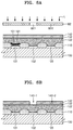
After the above-described first unit process is performed, a second unit process of forming the second organic functional layer 152 (see FIG. 6D) that emits color light different from that of the first organic functional layer 151 in an area where the second anode 101 is located is performed. The second unit process will now be explained with reference to FIGS. 6A through 6E.
Referring to FIG. 6A, a second lift-off layer 122 including a fluoropolymer, a second barrier layer 132, and a second photoresist 142 are sequentially formed on a structure of FIG. 5E.
The fluoropolymer included in the second lift-off layer 122 may be a polymer having a fluorine content in a range of about 20 wt % to about 60 wt %. The second lift-off layer 122 may include a material that is the same as or different from that of the first lift-off layer 121. The second lift-off layer 122 may be formed by using coating, printing, or deposition.
The second barrier layer 132 is formed on the second lift-off layer 122. The second barrier layer 132 may prevent impurities from diffusing from the second photoresist 122 to the second lift-off layer 122. The second barrier layer 132 may include at least one from among a metal, metal oxide, metal nitride, metal oxynitride, and an alloy.
The second photoresist 142 is formed on the second barrier layer 132. A portion of the second photoresist 142 corresponding to the second anode 102 is exposed through a second photomask M2 including a region M21 through which light L is transmitted. Next, the exposed second photoresist 142 is developed.
Referring to FIG. 6B, the second photoresist 142 is patterned. A first portion 142-1 of the second photoresist 142 corresponding to the second anode 102 and subjected to exposure and development is removed and a second portion 142-2 other than the first portion 142-1 remains.
The second barrier layer 132 is patterned along with the second photoresist 142. The second barrier layer 132 is patterned by etching the second barrier layer 132 including an inorganic material by using a solution for developing the second photoresist 142. Since the second barrier layer 132 is etched by using a developing solution of the second photoresist 142, the process may be simplified.
Propylene glycol methyl ether acetate (PGMEA) that is used as a solvent of the second photoresist 142 may diffuse to the second lift-off layer 122 and may degrade the first organic functional layer 151 that is formed in the first unit process. Oxygen or moisture, as well as PGMEA, may also diffuse to the second lift-off layer 122 and may degrade the first organic functional layer 151 that is formed in the first unit process.
However, in the present exemplary embodiment, since the second barrier layer 132 is formed between the second lift-off layer 122 and the second photoresist 142, PGMEA, moisture, and oxygen may be prevented from diffusing to the second lift-off layer 122 while the second photoresist 142 is developed. Accordingly, degradation of the first organic functional layer 151 may be reduced or prevented.
A thickness of the second barrier layer 132 may be equal to or greater than 200 Å and equal to or less than 1000 Å. When a thickness of the second barrier layer 132 is less than 200 Å, the second barrier layer 132 may not efficiently function as a barrier film due to a high water vapor transmission rate, and when a thickness of the second barrier layer 132 is greater than 1000 Å, it is difficult to etch the second barrier layer 132 while the second photoresist 142 is developed.
FIG. 11 is a graph illustrating a relationship between a water vapor transmission rate (WVTR) and a time when a thickness of the second barrier layer 132 is changed. FIG. 11 is a graph illustrating a relationship between a WVTR and a time when the second barrier layer 132 was formed of aluminum on the second lift-off layer 122 to some thicknesses.
It is found that a WVTR of each of a sample S200 in which a thickness of the second barrier layer 132 was 200 Å, a sample S300 in which a thickness of the second barrier layer 132 was 300 Å, a sample S400 in which a thickness of the second barrier layer 132 was 400 Å, a sample S500 in which a thickness of the second barrier layer 132 was 500 Å, and a sample S1000 in which a thickness of the second barrier layer 132 was 1000 Å is much lower than that of a reference sample REF having no second barrier layer.
Referring to FIG. 6C, the second lift-off layer 122 is etched by using a pattern of the second barrier layer 132 and the second photoresist 142 of FIG. 6B as an etch mask.
Since the second lift-off layer 122 includes the fluoropolymer, a solvent capable of etching the fluoropolymer is used as an etching solution.
A first solvent (not shown) including fluorine may be used as the etching solution. The first solvent may include hydrofluoroether. Hydrofluoroether is electrochemically stable because of its low interaction with other materials and environmentally stable because of its low global warming potential and low toxicity.
During an etching process, a portion of the second lift-off layer 122 corresponding to the first portion 142-1, that is, formed over the second anode 102, is etched.
When the second lift-off layer 122 is etched, a second undercut profile UC2 is formed in the second lift-off layer 122 under a boundary surface of the first portion 142-1 of the second photoresist 142 due to the first solvent including the fluorine. A delicate deposition pattern of the second organic functional layer 152 may be formed in a deposition process due to the second undercut profile UC2.
During the etching process, a portion of the second lift-off layer 122 corresponding to the first portion 142-1, that is, formed over the second anode 102, is etched to expose an upper portion of the second anode 102.
After the etching process, the exposed second anode 102 is subjected to second plasma treatment PT2. A residue of the second lift-off layer 122 that may remain on the second anode 102 may be removed due to the second plasma treatment PT2.
Ultraviolet rays generated during the second plasma treatment PT2 may degrade the first organic functional layer 151 that is formed in the first unit process. However, in the present exemplary embodiment, the second barrier layer 132 formed on the first organic functional layer 151 may protect the first organic functional layer 151 by blocking ultraviolet rays while the second plasma treatment PT2 is performed.
Referring to FIG. 6D, the second organic functional layer 152 including a second emission layer (not shown) and the second auxiliary cathode 182 are sequentially formed on the structure of FIG. 6C.
The second organic functional layer 152 may further include at least one functional layer from among a hole injection layer, a hole transport layer, an electron transport layer, and an electron injection layer.
The second organic functional layer 152 may be formed by using vapor deposition. In a deposition process, the second barrier layer 132, the second lift-off layer 122, and the second photoresist 142 function as a deposition mask. A part of the second organic functional layer 152 is formed at a position corresponding to the first portion 142-1, that is, over the second anode 102, and another part of the second organic functional layer 152 is formed on the second portion 142-2 of the second photoresist 142.
The second auxiliary cathode 182 may be formed by using vapor deposition, like the second organic functional layer 152. In a deposition process, the second barrier layer 132, the second lift-off layer 122, and the second photoresist 142 function as a deposition mask. A part of the second auxiliary cathode 182 is formed to cover a top surface of the second organic functional layer 152. Another part of the second auxiliary cathode 182 is formed on the second organic functional layer 152 to correspond to the second portion 142-2 other than the first portion 142-1 of the second photoresist 142.
The second auxiliary cathode 182 may include a material that is the same as that of the cathode 180 that is a common electrode. Alternatively, the second auxiliary cathode 182 may be formed of a material that is different from that of the cathode 180. The second auxiliary cathode 182 may function as a barrier for protecting the second organic functional layer 152 from a solvent used in a lift-off process.
Referring to FIG. 6E, a lift-off process is performed on a structure of FIG. 6D.
Since the second lift-off layer 122 includes the fluoropolymer, a second solvent including fluorine is used in the lift-off process. Since the second organic functional layer 152 is formed and then the lift-off process is performed, the second solvent should have a low reactivity to the second organic functional layer 152. The second solvent may include hydrofluoroether, similar to the first solvent.
When the second lift-off layer 122 formed under the second portion 142-2 (see FIG. 6B) of the second photoresist 142 is lifted off, the second organic functional layer 152 and the second auxiliary cathode 182 formed on the second portion 142-2 (see FIG. 6B) of the second photoresist 142 are removed, and the second organic functional layer 152 and the second auxiliary cathode 182 formed on the second anode 102 remain as a pattern.
After the above-described second unit process is performed, a third unit process of forming the third organic functional layer 153 that emits color light different from that of the first organic functional layer 151 and the second organic functional layer 152 in an area where the third anode 103 is located is performed. The third unit process will now be explained with reference to FIGS. 7A through 7E.
Referring to FIG. 7A, a third lift-off layer 123 including a fluoropolymer, a third barrier layer 133, and a third photoresist 143 are sequentially formed on a structure of FIG. 6E.
The fluoropolymer included in the third lift-off layer 123 may be a polymer having a fluorine content in a range of about 20 wt % to about 60 wt %. The third lift-off layer 123 may include a material that is the same as, or different from, that of the second lift-off layer 122. The third lift-off layer 123 may be formed by using coating, printing, or deposition.
The third barrier layer 133 is formed on the third lift-off layer 123. The third barrier layer 133 may prevent impurities from diffusing from the third photoresist 123 to the third lift-off layer 123. The third barrier layer 133 may include at least one from among a metal, metal oxide, metal nitride, metal oxynitride, and an alloy. Also, the third barrier layer 133 may include at least one from among silicon nitride, silicon oxide, and silicon oxynitride.
The third photoresist 143 is formed on the third barrier layer 133. A portion of the third photoresist 143 corresponding to the third anode 103 is exposed through a third photomask M3 including a region M31 through which light L is transmitted. Next, the exposed third photoresist 143 is developed.
Referring to FIG. 7B, the third photoresist 143 is patterned. A first portion 143-1 of the third photoresist 143 corresponding to the third anode 103 and subjected to exposure and development is removed and a second portion 143-2 remains.
The third barrier layer 133 is patterned along with the third photoresist 143. The third barrier layer 133 is patterned by etching the third barrier layer 133 including an inorganic material by using a solution for developing the third photoresist 143. Since the third barrier layer 133 is etched by using a developing solution of the third photoresist 143, a process may be simplified.
PGMEA that is used as a solvent of the third photoresist 143 may diffuse to the third lift-off layer 123, and may degrade the first organic functional layer 151 and the second organic functional layer 152 that are formed in the first and second unit processes. Also, oxygen or moisture, as well as PGMEA, may diffuse to the third lift-off layer 123, and may degrade the first organic functional layer 151 and the second organic functional layer 152 that are formed in the first and second unit processes.
However, in the present exemplary embodiment, since the third barrier layer 133 is formed between the third lift-off layer 123 and the third photoresist 143, PGMEA, oxygen, or moisture may be prevented from diffusing to the third lift-off layer 123 while the third photoresist 143 is developed. Accordingly, degradation of the first organic functional layer 151 and the second organic functional layer 152 may be reduced or prevented.
Referring to FIG. 7C, the third lift-off layer 123 is etched by using a pattern of the third barrier layer 133 and the third photoresist 143 of FIG. 7B as an etch mask.
Since the third lift-off layer 123 includes the fluoropolymer, a solvent capable for etching the fluoropolymer is used as an etching solution.
A first solvent (not shown) including fluorine may be used as the etching solution. The first solvent may include hydrofluoroether. Hydrofluoroether is electrochemically stable because of its low interaction with other materials and environmentally stable because of its low global warming potential and low toxicity.
During an etching process, a portion of the third lift-off layer 123 corresponding to the first portion 143-1, that is, formed over the third anode 103, is etched.
When the third lift-off layer 123 is etched, a third undercut profile UC3 is formed in the third lift-off layer 132 under a boundary surface of the first portion 143-1 of the third photoresist 143 due to the first solvent. A delicate deposition pattern of the third organic functional layer 153 may be formed in a deposition process due to the third undercut profile UC3.
During an etching process, a portion of the third lift-off layer 123 corresponding to the first portion 143-1, that is, formed over the third anode 103, is etched to expose an upper portion of the third anode 103.
After the etching process, the exposed third anode 103 is subjected to third plasma treatment PT3. A residue of the third lift-off layer 123 that may remain on the third anode 103 may be removed due to the third plasma treatment PT3.
Ultraviolet rays generated during the third plasma treatment PT3 may degrade the first organic functional layer 151 and the second organic functional layer 152 that are formed in the first and second unit processes. However, in the present exemplary embodiment, the third barrier layer 133 formed on the first organic functional layer 151 and the second organic functional layer 152 may protect the first organic functional layer 151 and the second organic functional layer 152 by blocking ultraviolet rays while the third plasma treatment PT3 is performed.
Referring to FIG. 7D, the third organic functional layer 153, including a third emission layer (not shown) and the third auxiliary cathode 183, are sequentially formed on the structure of FIG. 7C.
The third organic functional layer 153 may further include at least one functional layer from among a hole injection layer, a hole transport layer, an electron transport layer, and an electron injection layer.
The third organic functional layer 153 may be formed by using vapor deposition. In a deposition process, the third barrier layer 133, the third lift-off layer 123, and the third photoresist 143 function as a deposition mask. A part of the third organic functional layer 153 is formed at a position corresponding to the first portion 143-1, that is, over the third anode 103, and another part of the third organic functional layer 153 is formed on the second portion 143-2 of the third photoresist 143.
The third auxiliary cathode 183 may be formed by using vapor deposition, like the third organic functional layer 153. In a deposition process, the third barrier layer 133, the third lift-off layer 123, and the third photoresist 143 function as a deposition mask. A part of the third auxiliary cathode 183 is formed to cover a top surface of the third organic functional layer 153. Another part of the third auxiliary cathode 183 is formed on the third organic functional layer 153 to correspond to the second portion 143-2 other than the first portion 143-1 of the third photoresist 143.
The third auxiliary cathode 183 may include a material that is the same as that of the cathode 180 that is a common electrode. Alternatively, the third auxiliary cathode 183 may include a material that is different from that of the cathode 180. The third auxiliary cathode 183 may function as a barrier for protecting the third organic functional layer 153 from a solvent that is used in a lift-off process.
Referring to FIG. 7E, a lift-off process is performed on a structure of FIG. 7D.
Since the third barrier layer 133 and the third lift-off layer 123 include the fluoropolymer, a second solvent including fluorine is used in the lift-off process. Since the third organic functional layer 153 is formed and then the lift-off process is performed, the second solvent should have a low reactivity to the third organic functional layer 153. The second solvent may include hydrofluoroether, like the first solvent.
When the third lift-off layer 123 formed under the second portion 143-2 (see FIG. 7B) of the third photoresist 143 is lifted off, the third organic functional layer 153 and the third auxiliary cathode 183 formed on the second portion 143-2 (see FIG. 7B) of the third photoresist 143 are removed and the third organic functional layer 153 and the third auxiliary cathode 183 formed on the third anode 103 remain as a pattern.
After the above-described third unit process, the cathode 180 (see FIG. 2) that is a common layer is formed on the first through third auxiliary cathodes 181, 182, and 183. The first through third auxiliary cathodes 181, 182, and 183 may prevent a voltage drop of a cathode.
Although the first through third anodes 101, 102, and 103 are hole injection electrodes, and the first through third auxiliary cathodes 181, 182, and 183 are electron injection electrodes in the present exemplary embodiment, the inventive concepts are not limited thereto, and electron injection electrodes may be formed in an area where the first through third anodes 101, 102, and 103 are located, and hole injection electrodes may be formed in an area where the first through third auxiliary cathodes 181, 182, and 183 are located.
The first through third organic functional layers 151, 152, and 153 may emit light of different colors. Light emitted by the first through third organic functional layers 151, 152, and 153 may be mixed together to form white light. For example, the first through third organic functional layers 151, 152, and 153 may respectively emit red light, green light, and blue light. For example, the first through third organic functional layers 151, 152, and 153 may be elements of sub-pixels constituting a unit pixel of the organic light-emitting display apparatus 1.
The organic light-emitting display apparatus 1 of FIG. 2 may indicate one unit pixel. The present exemplary embodiment may be applied to an organic light-emitting display apparatus including a plurality of the unit pixels of FIG. 1. That is, a plurality of the first organic functional layers 151 that emit light of a first color may be simultaneously formed as a first group in a first unit process. A plurality of the second organic functional layers 152 that emit light of a second color may be simultaneously formed as a second group in a second unit process. A plurality of the third organic functional layers 153 that emit light of a third color may be simultaneously formed as a third group in a third unit process. A full-color image may be formed by using the first through third unit processes.
Although a barrier layer is formed in second and third unit processes and is not formed in a first unit process in the present exemplary embodiment, the inventive concepts are not limited thereto, and a barrier layer may also be formed in the first unit process. A process may be simplified by performing the first through third unit processes in the same manner.
A method of manufacturing an organic light-emitting display apparatus according to a comparative example of FIGS. 8A through 10E will now be explained for comparison.
FIGS. 8A through 8E are cross-sectional views for explaining a first unit process of an organic light-emitting display apparatus according to a comparative example. FIG. 9A through 9E are cross-sectional views for explaining a second unit process of the organic light-emitting display apparatus according to the comparative example. FIGS. 10A through 10E are cross-sectional views for explaining a third unit process of the organic light-emitting display apparatus according to the comparative example.
Referring to FIG. 8A, the first lift-off layer 121 including a fluoropolymer is formed on the substrate 100 on which the first through third anodes 101, 102, and 103 are formed, and the first photoresist 141 is formed on the first lift-off layer 121.
Referring to FIG. 8B, the first photoresist 141 is patterned. The first portion 141-1 of the first photoresist 141 corresponding to the first anode 101 and subjected to exposure and development is removed and the second portion 141-2 other than the first portion 141-1 remains.
Referring to FIG. 8C, the first lift-off layer 121 is etched by using a first solvent (not shown) including fluorine by using a pattern of the first photoresist 141 of FIG. 7B as an etch mask. During an etching process, a portion of the first lift-off layer 121 corresponding to the first portion 141-1, that is, formed over the first anode 101, is etched. The first undercut profile UC1 is formed in the first lift-off layer 121 under a boundary surface of the first portion 141-1 of the first photoresist 141. After the etching process, the first plasma treatment PT1 is performed on the exposed first anode 101.
Referring to FIG. 8D, the first organic functional layer 151 and the first auxiliary cathode 181 are sequentially formed on a structure of FIG. 8C.
Referring to FIG. 8E, the first lift-off layer 121 that remains is completely removed by performing a first lift-off process, and thus the first organic functional layer 151 and the first auxiliary cathode 181 on the first anode 101 remain as a pattern.
After the above-described first unit process ends, a second unit process is performed in an area where the second anode 102 is located.
Referring to FIG. 9A, the second lift-off layer 122 and the second photoresist 142 are sequentially formed on the structure of FIG. 8E.
Referring to FIG. 9B, the second photoresist 142 is exposed and developed to remove the first portion 142-1 of the second photoresist 142 corresponding to the second anode 102 and to leave the second portion 142-2 other than the first portion 142-1.
The second lift-off layer 122 includes a fluoropolymer. Although the fluoropolymer is electrochemically stable because of its low interaction with other materials, PGMEA, moisture, or oxygen (e.g., P1 or P2) included in the second photoresist 142 may diffuse to the second lift-off layer 122 and may degrade the first organic functional layer 151.
Referring to FIG. 9C, the second lift-off layer 122 is etched by using a first solvent (not shown) including fluorine by using a pattern of the second photoresist 142 of FIG. 9B as an etch mask. During an etching process, a portion of the second lift-off layer 122 corresponding to the first portion 142-1, that is, formed over the second anode 102, is etched. The second undercut profile UC2 is formed in the second lift-off layer 122 under a boundary surface of the first portion 142-1 of the second photoresist 142.
After the etching process, the second plasma treatment PT2 is performed on the exposed second anode 102 in order to remove a residue of the second lift-off layer 122. Ultraviolet rays that are generated during the second plasma treatment PT2 may degrade the first organic functional layer 151.
Referring to FIG. 9D, the second organic functional layer 152 and the second auxiliary cathode 182 are sequentially formed on a structure of FIG. 9C.
Referring to FIG. 9E, the second lift-off layer 122 that remains is completely removed by performing a second lift-off process, and thus, the first organic functional layer 151 and the first auxiliary cathode 181 on the first anode 101 and the second organic functional layer 152 and the second auxiliary cathode 182 on the second anode 102 remain as a pattern.
After the above-described second unit process ends, a third unit process is performed in an area where the third anode 103 is located.
Referring to FIG. 10A, the third lift-off layer 123 and the third photoresist 143 are sequentially formed on the structure of FIG. 9E.
Referring to FIG. 10B, the third photoresist 143 is patterned, and the first portion 143-1 of the third photoresist 143 corresponding to the third anode 103 and subjected to exposure and development is removed and the second portion 143-2 other than the first portion 143-1 remains.
The third lift-off layer 123 includes a fluoropolymer. Although the fluoropolymer is electrochemically stable because of its low interaction with other materials, PGMEA, moisture, or oxygen (e.g., P1, P2, or P3) included in the third photoresist 143 may diffuse to the third lift-off layer 123 and may degrade the first organic functional layer 151 and the second organic functional layer 152.
Referring to FIG. 10C, the third lift-off layer 123 is etched by using a first solvent (not shown) including fluorine by using a pattern of the third photoresist 143 of FIG. 10B as an etch mask. During an etching process, a portion of the third lift-off layer 123 corresponding to the first portion 143-1, that is, formed over the third anode 103, is etched. The third undercut profile UC3 is formed in the third lift-off layer 123 under a boundary surface of the first portion 143-1 of the third photoresist 143.
After the etching process, the third plasma treatment PT3 is performed on the exposed third anode 103 in order to remove a residue of the third lift-off layer 123. Ultraviolet rays that are generated during the third plasma treatment PT3 may degrade the first organic functional layer 151 and the second organic functional layer 152 that are formed in the first and second unit processes.
Referring to FIG. 10D, the third organic functional layer 153 and the third auxiliary cathode 183 are sequentially formed on a structure of FIG. 10C.
Referring to FIG. 10E, the third lift-off layer 123 that remains is completely removed by performing a third lift-off process, and thus the first organic functional layer 151 and the first auxiliary cathode 181 on the first anode 101, the second organic functional layer 152 and the second auxiliary cathode 182 on the second anode 102, and the third organic functional layer 153 and the third auxiliary cathode 183 on the third anode 103 remain as a pattern.
Although not shown in the drawings, the organic light-emitting display apparatuses may further include an encapsulation member for encapsulating an organic emission layer. The encapsulation member may include a glass substrate, a metal foil, and a thin-film encapsulation layer in which an inorganic layer and an organic layer are combined.
According to an exemplary embodiment, since an emission layer is formed without using a fine metal mask (FMM), a high-resolution display panel may be formed.
Also, since an organic emission layer may be prevented from being degraded by forming a barrier layer between a lift-off layer including a fluoropolymer and a photoresist, the number of defects may be reduced.
Although certain exemplary embodiments and implementations have been described herein, other embodiments and modifications will be apparent from this description. Accordingly, the inventive concepts are not limited to such embodiments, but rather to the broader scope of the appended claims and various obvious modifications and equivalent arrangements as would be apparent to a person of ordinary skill in the art.

Claims (7)

What is claimed is:
1. A method of manufacturing an organic light-emitting display apparatus, the method comprising:
forming a plurality of first electrodes on a substrate and performing a first unit process comprising the steps of:
(a1) forming a first lift-off layer on the substrate comprising the plurality of first electrodes, the first lift-off layer comprising a fluoropolymer;
(b1) sequentially forming a first photoresist on the first lift-off layer;
(c1) patterning the first photoresist to remove a first portion of the first photoresist corresponding to the first electrodes of a first group such that a second portion other than the first portion remains;
(d1) etching a portion of the first lift-off layer corresponding to the first portion to expose the first electrodes of the first group;
(e1) sequentially forming a first organic functional layer and a first auxiliary electrode over the first electrodes of the first group and the second portion of the first photoresist, the first organic functional layer comprising a first emission layer; and
(f1) removing the first lift-off layer, the first photoresist, the first organic functional layer, and the first auxiliary electrode remaining on the second portion; and
after the performing of the first unit process, performing, at least once, a second unit process comprising the steps of:
(a2) forming a second lift-off layer on a resultant structure of step (f1), the second lift-off layer comprising a fluoropolymer;
(b2) forming a barrier layer and a second photoresist on the second lift-off layer, the barrier layer comprising an inorganic material;
(c2) patterning the second photoresist and the barrier layer to remove a first portion of the second photoresist corresponding to the first electrodes of a second group such that a second portion other than the first portion remains;
(d2) etching a portion of the second lift-off layer corresponding to the first portion to expose the first electrodes of the second group;
(e2) sequentially forming a second organic functional layer and a second auxiliary electrode over the first electrodes of the second group and the second portion of the second photoresist, the second organic functional layer comprising a second emission layer; and
(f2) removing the second lift-off layer, the barrier layer, the second photoresist, the second organic functional layer, and the second auxiliary electrode remaining on the second portion,
wherein:
after the first and second unit processes are performed, a second electrode is formed;
the barrier layer comprises a metal oxynitride; and
the barrier layer has a thickness greater than 200 Å and equal to or less than 1000 Å.
2. The method of claim 1, wherein colors of light emitted by the first organic functional layer and the second organic functional layer are different from each other.
3. The method of claim 1, wherein the etching of the portion of the first lift-off layer in step (d1) and the etching of the portion of the second lift-off layer in step (d2) are performed by using wet etching using a first solvent comprising fluorine.
4. The method of claim 3, wherein in steps (d1) and (d2), after the wet etching using the first solvent, plasma treatment is performed on the exposed first electrodes of the first group and the exposed second electrode of the second group.
5. The method of claim 1, wherein the removing of the first lift-off layer, the first photoresist, the first organic functional layer, and the first auxiliary electrode in step (f1) and the removing of the second lift-off layer, the barrier layer, the second photoresist, the second organic functional layer, and the second auxiliary electrode in step (f2) are performed by using a second solvent comprising fluorine.
6. The method of claim 1, wherein the second electrode is commonly formed on the first auxiliary electrode and the second auxiliary electrode.
7. A method of manufacturing an organic light-emitting display apparatus, the method comprising:
forming a plurality of first electrodes on a substrate and performing a first unit process comprising the steps of:
(a1) forming a first lift-off layer on the substrate comprising the plurality of first electrodes, the first lift-off layer comprising a fluoropolymer;
(b1) sequentially forming a first photoresist directly on the first lift-off layer;
(c1) patterning the first photoresist to remove a first portion of the first photoresist corresponding to the first electrodes of a first group such that a second portion other than the first portion remains;
(d1) etching a portion of the first lift-off layer corresponding to the first portion to expose the first electrodes of the first group;
(e1) sequentially forming a first organic functional layer and a first auxiliary electrode over the first electrodes of the first group and the second portion of the first photoresist, the first organic functional layer comprising a first emission layer; and
(f1) removing the first lift-off layer, the first photoresist, the first organic functional layer, and the first auxiliary electrode remaining on the second portion; and
after the performing of the first unit process, performing, at least once, a second unit process comprising the steps of:
(a2) forming a second lift-off layer on a resultant structure of step (f1), the second lift-off layer comprising a fluoropolymer;
(b2) forming a barrier layer directly on the second lift-off layer and a second photoresist directly on the barrier layer, the barrier layer comprising an inorganic material;
(c2) patterning the second photoresist and the barrier layer to remove a first portion of the second photoresist corresponding to the first electrodes of a second group such that a second portion other than the first portion remains;
(d2) etching a portion of the second lift-off layer corresponding to the first portion to expose the first electrodes of the second group;
(e2) sequentially forming a second organic functional layer and a second auxiliary electrode over the first electrodes of the second group and the second portion of the second photoresist, the second organic functional layer comprising a second emission layer; and
(f2) removing the second lift-off layer, the barrier layer, the second photoresist, the second organic functional layer, and the second auxiliary electrode remaining on the second portion,
wherein:
after the first and second unit processes are performed, a second electrode is formed;
the barrier layer comprises a metal oxynitride; and
the barrier layer has a thickness greater than 200 Å and equal to or less than 1000 Å.
US16/549,413 2017-01-03 2019-08-23 Organic light-emitting display apparatus and method of manufacturing the same Active US11127902B2 (en)

Priority Applications (1)

Application Number Priority Date Filing Date Title
US16/549,413 US11127902B2 (en) 2017-01-03 2019-08-23 Organic light-emitting display apparatus and method of manufacturing the same

Applications Claiming Priority (4)

Application Number Priority Date Filing Date Title
KR10-2017-0000791 2017-01-03
KR1020170000791A KR20180080416A (en) 2017-01-03 2017-01-03 Organic light-emitting apparatus and the method for manufacturing of the organic light-emitting display apparatus
US15/860,466 US10431742B2 (en) 2017-01-03 2018-01-02 Organic light-emitting display apparatus and method of manufacturing the same
US16/549,413 US11127902B2 (en) 2017-01-03 2019-08-23 Organic light-emitting display apparatus and method of manufacturing the same

Related Parent Applications (1)

Application Number Title Priority Date Filing Date
US15/860,466 Division US10431742B2 (en) 2017-01-03 2018-01-02 Organic light-emitting display apparatus and method of manufacturing the same

Publications (2)

Publication Number Publication Date
US20190378986A1 US20190378986A1 (en) 2019-12-12
US11127902B2 true US11127902B2 (en) 2021-09-21

Family

ID=62711317

Family Applications (2)

Application Number Title Priority Date Filing Date
US15/860,466 Active US10431742B2 (en) 2017-01-03 2018-01-02 Organic light-emitting display apparatus and method of manufacturing the same
US16/549,413 Active US11127902B2 (en) 2017-01-03 2019-08-23 Organic light-emitting display apparatus and method of manufacturing the same

Family Applications Before (1)

Application Number Title Priority Date Filing Date
US15/860,466 Active US10431742B2 (en) 2017-01-03 2018-01-02 Organic light-emitting display apparatus and method of manufacturing the same

Country Status (2)

Country Link
US (2) US10431742B2 (en)
KR (1) KR20180080416A (en)

Cited By (1)

* Cited by examiner, † Cited by third party
Publication number Priority date Publication date Assignee Title
US11871591B2 (en) 2018-11-07 2024-01-09 Samsung Display Co., Ltd. Organic light-emitting display device and a method of manufacturing the same

Families Citing this family (20)

* Cited by examiner, † Cited by third party
Publication number Priority date Publication date Assignee Title
US10217819B2 (en) 2015-05-20 2019-02-26 Samsung Electronics Co., Ltd. Semiconductor device including metal-2 dimensional material-semiconductor contact
KR102603867B1 (en) * 2016-08-01 2023-11-21 삼성디스플레이 주식회사 Organic light-emitting apparatus and the method for manufacturing of the organic light-emitting display apparatus
US10461139B2 (en) * 2016-11-10 2019-10-29 Int Tech Co., Ltd. Light emitting device manufacturing method and apparatus thereof
US10193098B2 (en) * 2016-11-10 2019-01-29 Int Tech Co., Ltd. Light emitting device manufacturing method and apparatus thereof
KR102278608B1 (en) * 2017-03-10 2021-07-19 삼성디스플레이 주식회사 Organic light-emitting apparatus and the method for manufacturing of the organic light-emitting display apparatus
US10700299B2 (en) * 2017-08-01 2020-06-30 Zixu Optronics Technology (Shanghai) Limited Method for manufacturing organic light emitting diode using conductive protective layer
US10438848B2 (en) * 2017-11-01 2019-10-08 Semi Automation & Technologies, Inc. Inorganic lift-off profile process for semiconductor wafer processing
US20190196285A1 (en) * 2017-12-26 2019-06-27 Shenzhen China Star Optoelectronics Semiconductor Display Technology Co., Ltd. Manufacturing method of array substrate and its upper electrode line pattern and liquid crystal display panel
KR102614588B1 (en) 2018-08-20 2023-12-18 삼성디스플레이 주식회사 Method of manufacturing display apparatus
US20220020830A1 (en) * 2018-11-19 2022-01-20 Dinguo Chen Patterning of Organic Light Emitting Diode Device and the OLED Displays Manufactured Therefrom
CN109585343B (en) * 2018-11-30 2021-04-30 京东方科技集团股份有限公司 Stripping method of packaging film layer in display panel
CN111276618A (en) * 2018-12-05 2020-06-12 陕西坤同半导体科技有限公司 Organic functional layer, method for preparing organic functional layer and display panel
KR20200080491A (en) 2018-12-26 2020-07-07 삼성디스플레이 주식회사 Organic light emitting display apparatus and method of manufacturing the same
CN110024157A (en) * 2019-03-01 2019-07-16 京东方科技集团股份有限公司 The manufacturing method of array substrate, display panel and array substrate
KR20200109435A (en) 2019-03-12 2020-09-23 삼성디스플레이 주식회사 Display apparatus and method of manufacturing the same
CN112002817B (en) * 2020-08-25 2022-09-09 视涯科技股份有限公司 Organic light-emitting display panel
CN112420798B (en) * 2020-11-19 2023-04-18 安徽熙泰智能科技有限公司 Preparation method of silicon-based OLED panel
CN113725390A (en) * 2021-08-30 2021-11-30 京东方科技集团股份有限公司 Display substrate, preparation method thereof and display device
JP2024006463A (en) * 2022-07-01 2024-01-17 キヤノントッキ株式会社 Manufacturing method for electronic device and film deposition method
JP2024006462A (en) * 2022-07-01 2024-01-17 キヤノントッキ株式会社 Film deposition device, film deposition method, and manufacturing method for electronic device

Citations (10)

* Cited by examiner, † Cited by third party
Publication number Priority date Publication date Assignee Title
US4519872A (en) * 1984-06-11 1985-05-28 International Business Machines Corporation Use of depolymerizable polymers in the fabrication of lift-off structure for multilevel metal processes
US4826564A (en) 1987-10-30 1989-05-02 International Business Machines Corporation Method of selective reactive ion etching of substrates
JP2002170669A (en) 2000-12-01 2002-06-14 Tdk Corp Organic el display device and its manufacturing method
US20050054194A1 (en) * 2003-09-08 2005-03-10 Taiwan Semiconductor Manufacturing Co., Ltd., Method for forming dual damascenes
US20050202351A1 (en) 2004-03-09 2005-09-15 Houlihan Francis M. Process of imaging a deep ultraviolet photoresist with a top coating and materials thereof
US20060035015A1 (en) 2004-08-10 2006-02-16 Eastman Kodak Company Making a cathode structure for OLEDS
WO2008038588A1 (en) 2006-09-28 2008-04-03 Rohm Co., Ltd. Method for manufacturing organic material apparatus
US20080166667A1 (en) 2006-08-08 2008-07-10 International Business Machines Tunable contact angle process for immersionlithography topcoats and photoresists
US8853095B1 (en) * 2013-05-30 2014-10-07 International Business Machines Corporation Hybrid hard mask for damascene and dual damascene
US20170256754A1 (en) * 2014-08-01 2017-09-07 Orthogonal, Inc. Photolithographic patterning of organic electronic devices

Patent Citations (12)

* Cited by examiner, † Cited by third party
Publication number Priority date Publication date Assignee Title
US4519872A (en) * 1984-06-11 1985-05-28 International Business Machines Corporation Use of depolymerizable polymers in the fabrication of lift-off structure for multilevel metal processes
US4826564A (en) 1987-10-30 1989-05-02 International Business Machines Corporation Method of selective reactive ion etching of substrates
JP2002170669A (en) 2000-12-01 2002-06-14 Tdk Corp Organic el display device and its manufacturing method
US20050054194A1 (en) * 2003-09-08 2005-03-10 Taiwan Semiconductor Manufacturing Co., Ltd., Method for forming dual damascenes
US20050202351A1 (en) 2004-03-09 2005-09-15 Houlihan Francis M. Process of imaging a deep ultraviolet photoresist with a top coating and materials thereof
JP2007528511A (en) 2004-03-09 2007-10-11 エイゼット・エレクトロニック・マテリアルズ・ユーエスエイ・コーポレイション US Patent Application Serial No. 10 / 796,376, filed March 9, 2004, which is a cross-reference of a method for forming an image in a deep UV photoresist using a top coat and a material related application therefor. This is a continuation-in-part of US patent application serial number 10 / 875,596 filed on June 24, 2004, which is a continuation-in-part. The contents of these application specifications shall be published in this specification.
US20060035015A1 (en) 2004-08-10 2006-02-16 Eastman Kodak Company Making a cathode structure for OLEDS
US20080166667A1 (en) 2006-08-08 2008-07-10 International Business Machines Tunable contact angle process for immersionlithography topcoats and photoresists
WO2008038588A1 (en) 2006-09-28 2008-04-03 Rohm Co., Ltd. Method for manufacturing organic material apparatus
JP2008085200A (en) 2006-09-28 2008-04-10 Kyoto Univ Manufacturing method of organic material equipment
US8853095B1 (en) * 2013-05-30 2014-10-07 International Business Machines Corporation Hybrid hard mask for damascene and dual damascene
US20170256754A1 (en) * 2014-08-01 2017-09-07 Orthogonal, Inc. Photolithographic patterning of organic electronic devices

Non-Patent Citations (3)

* Cited by examiner, † Cited by third party
Title
Final Office Action dated Apr. 9, 2019, issued in U.S. Appl. No. 15/860,466.
Non-Final Office Action dated Nov. 30, 2018, issued in U.S. Appl. No. 15/860,466.
Notice of Allowance dated Jun. 6, 2019, issued in U.S. Appl. No. 15/860,466.

Cited By (1)

* Cited by examiner, † Cited by third party
Publication number Priority date Publication date Assignee Title
US11871591B2 (en) 2018-11-07 2024-01-09 Samsung Display Co., Ltd. Organic light-emitting display device and a method of manufacturing the same

Also Published As

Publication number Publication date
US10431742B2 (en) 2019-10-01
KR20180080416A (en) 2018-07-12
US20190378986A1 (en) 2019-12-12
US20180190907A1 (en) 2018-07-05

Similar Documents

Publication Publication Date Title
US11127902B2 (en) Organic light-emitting display apparatus and method of manufacturing the same
US10693068B2 (en) Organic light-emitting display apparatus and method of manufacturing the same
US10862034B2 (en) Organic light-emitting display apparatus and method of manufacturing the same
US11758768B2 (en) Organic light-emitting display apparatus comprising self-assembled layer containing fluorine
US11469374B2 (en) Organic light-emitting display apparatus and method of manufacturing the same
US10930875B2 (en) Organic light-emitting display apparatus and method of manufacturing the same
US10985339B2 (en) Organic light-emitting display apparatus and method of manufacturing the same
US10134991B2 (en) Organic light-emitting display apparatus and method of manufacturing the same
US10431744B2 (en) Method of manufacturing organic light-emitting display apparatus using barrier layer having high fluorine content

Legal Events

Date Code Title Description
FEPP Fee payment procedure

Free format text: ENTITY STATUS SET TO UNDISCOUNTED (ORIGINAL EVENT CODE: BIG.); ENTITY STATUS OF PATENT OWNER: LARGE ENTITY

STPP Information on status: patent application and granting procedure in general

Free format text: DOCKETED NEW CASE - READY FOR EXAMINATION

STPP Information on status: patent application and granting procedure in general

Free format text: NON FINAL ACTION MAILED

STPP Information on status: patent application and granting procedure in general

Free format text: RESPONSE TO NON-FINAL OFFICE ACTION ENTERED AND FORWARDED TO EXAMINER

STPP Information on status: patent application and granting procedure in general

Free format text: ADVISORY ACTION MAILED

STPP Information on status: patent application and granting procedure in general

Free format text: NON FINAL ACTION MAILED

STPP Information on status: patent application and granting procedure in general

Free format text: RESPONSE TO NON-FINAL OFFICE ACTION ENTERED AND FORWARDED TO EXAMINER

STPP Information on status: patent application and granting procedure in general

Free format text: NOTICE OF ALLOWANCE MAILED -- APPLICATION RECEIVED IN OFFICE OF PUBLICATIONS

STPP Information on status: patent application and granting procedure in general

Free format text: PUBLICATIONS -- ISSUE FEE PAYMENT VERIFIED

STCF Information on status: patent grant

Free format text: PATENTED CASE