US10693068B2 - Organic light-emitting display apparatus and method of manufacturing the same - Google Patents
Organic light-emitting display apparatus and method of manufacturing the same Download PDFInfo
- Publication number
- US10693068B2 US10693068B2 US15/657,439 US201715657439A US10693068B2 US 10693068 B2 US10693068 B2 US 10693068B2 US 201715657439 A US201715657439 A US 201715657439A US 10693068 B2 US10693068 B2 US 10693068B2
- Authority
- US
- United States
- Prior art keywords
- layer
- lift
- electrode
- organic functional
- electrodes
- Prior art date
- Legal status (The legal status is an assumption and is not a legal conclusion. Google has not performed a legal analysis and makes no representation as to the accuracy of the status listed.)
- Active
Links
- 238000004519 manufacturing process Methods 0.000 title claims abstract description 11
- 239000010410 layer Substances 0.000 claims abstract description 127
- 239000002346 layers by function Substances 0.000 claims abstract description 108
- 239000000758 substrate Substances 0.000 claims abstract description 27
- 238000000034 method Methods 0.000 claims description 85
- 229920002120 photoresistant polymer Polymers 0.000 claims description 69
- 239000000463 material Substances 0.000 claims description 41
- 229910052709 silver Inorganic materials 0.000 claims description 41
- 239000004332 silver Substances 0.000 claims description 41
- BQCADISMDOOEFD-UHFFFAOYSA-N Silver Chemical compound [Ag] BQCADISMDOOEFD-UHFFFAOYSA-N 0.000 claims description 39
- 239000002904 solvent Substances 0.000 claims description 34
- 239000004811 fluoropolymer Substances 0.000 claims description 18
- 229920002313 fluoropolymer Polymers 0.000 claims description 18
- 238000002347 injection Methods 0.000 claims description 16
- 239000007924 injection Substances 0.000 claims description 16
- 238000005137 deposition process Methods 0.000 claims description 14
- 229910052731 fluorine Inorganic materials 0.000 claims description 10
- 239000011737 fluorine Substances 0.000 claims description 10
- 230000005525 hole transport Effects 0.000 claims description 5
- PXGOKWXKJXAPGV-UHFFFAOYSA-N Fluorine Chemical compound FF PXGOKWXKJXAPGV-UHFFFAOYSA-N 0.000 claims 1
- 230000008569 process Effects 0.000 description 59
- 239000010408 film Substances 0.000 description 27
- 229910052751 metal Inorganic materials 0.000 description 17
- 239000002184 metal Substances 0.000 description 17
- 230000007547 defect Effects 0.000 description 15
- -1 poly(methyl methacrylate) Polymers 0.000 description 11
- 238000000151 deposition Methods 0.000 description 10
- 229920000642 polymer Polymers 0.000 description 10
- YCKRFDGAMUMZLT-UHFFFAOYSA-N Fluorine atom Chemical compound [F] YCKRFDGAMUMZLT-UHFFFAOYSA-N 0.000 description 9
- 239000002245 particle Substances 0.000 description 9
- 239000006096 absorbing agent Substances 0.000 description 8
- 238000005530 etching Methods 0.000 description 8
- 238000001771 vacuum deposition Methods 0.000 description 8
- 230000000052 comparative effect Effects 0.000 description 7
- 239000011368 organic material Substances 0.000 description 7
- 230000008021 deposition Effects 0.000 description 6
- 229910001316 Ag alloy Inorganic materials 0.000 description 5
- 229920001577 copolymer Polymers 0.000 description 5
- 229910010272 inorganic material Inorganic materials 0.000 description 5
- 238000000576 coating method Methods 0.000 description 4
- 238000005538 encapsulation Methods 0.000 description 4
- 239000011147 inorganic material Substances 0.000 description 4
- 150000002739 metals Chemical class 0.000 description 4
- 230000004888 barrier function Effects 0.000 description 3
- AMGQUBHHOARCQH-UHFFFAOYSA-N indium;oxotin Chemical compound [In].[Sn]=O AMGQUBHHOARCQH-UHFFFAOYSA-N 0.000 description 3
- 230000009257 reactivity Effects 0.000 description 3
- 239000004593 Epoxy Substances 0.000 description 2
- URLKBWYHVLBVBO-UHFFFAOYSA-N Para-Xylene Chemical group CC1=CC=C(C)C=C1 URLKBWYHVLBVBO-UHFFFAOYSA-N 0.000 description 2
- BLRPTPMANUNPDV-UHFFFAOYSA-N Silane Chemical compound [SiH4] BLRPTPMANUNPDV-UHFFFAOYSA-N 0.000 description 2
- VYPSYNLAJGMNEJ-UHFFFAOYSA-N Silicium dioxide Chemical compound O=[Si]=O VYPSYNLAJGMNEJ-UHFFFAOYSA-N 0.000 description 2
- GWEVSGVZZGPLCZ-UHFFFAOYSA-N Titan oxide Chemical compound O=[Ti]=O GWEVSGVZZGPLCZ-UHFFFAOYSA-N 0.000 description 2
- XLOMVQKBTHCTTD-UHFFFAOYSA-N Zinc monoxide Chemical compound [Zn]=O XLOMVQKBTHCTTD-UHFFFAOYSA-N 0.000 description 2
- MCMNRKCIXSYSNV-UHFFFAOYSA-N Zirconium dioxide Chemical compound O=[Zr]=O MCMNRKCIXSYSNV-UHFFFAOYSA-N 0.000 description 2
- 229910052782 aluminium Inorganic materials 0.000 description 2
- XAGFODPZIPBFFR-UHFFFAOYSA-N aluminium Chemical compound [Al] XAGFODPZIPBFFR-UHFFFAOYSA-N 0.000 description 2
- QVGXLLKOCUKJST-UHFFFAOYSA-N atomic oxygen Chemical compound [O] QVGXLLKOCUKJST-UHFFFAOYSA-N 0.000 description 2
- QVQLCTNNEUAWMS-UHFFFAOYSA-N barium oxide Chemical compound [Ba]=O QVQLCTNNEUAWMS-UHFFFAOYSA-N 0.000 description 2
- UUAGAQFQZIEFAH-UHFFFAOYSA-N chlorotrifluoroethylene Chemical group FC(F)=C(F)Cl UUAGAQFQZIEFAH-UHFFFAOYSA-N 0.000 description 2
- 239000003086 colorant Substances 0.000 description 2
- 230000005684 electric field Effects 0.000 description 2
- 239000011521 glass Substances 0.000 description 2
- 229910052760 oxygen Inorganic materials 0.000 description 2
- 239000001301 oxygen Substances 0.000 description 2
- 239000004033 plastic Substances 0.000 description 2
- 229920003023 plastic Polymers 0.000 description 2
- 229920003229 poly(methyl methacrylate) Polymers 0.000 description 2
- 239000004926 polymethyl methacrylate Substances 0.000 description 2
- 229910000077 silane Inorganic materials 0.000 description 2
- 229910052814 silicon oxide Inorganic materials 0.000 description 2
- BFKJFAAPBSQJPD-UHFFFAOYSA-N tetrafluoroethene Chemical group FC(F)=C(F)F BFKJFAAPBSQJPD-UHFFFAOYSA-N 0.000 description 2
- 239000010409 thin film Substances 0.000 description 2
- MSHXSYMNYJAOSS-UHFFFAOYSA-N 1,1-dichloro-2-fluoroethene Chemical group FC=C(Cl)Cl MSHXSYMNYJAOSS-UHFFFAOYSA-N 0.000 description 1
- OYPRJOBELJOOCE-UHFFFAOYSA-N Calcium Chemical compound [Ca] OYPRJOBELJOOCE-UHFFFAOYSA-N 0.000 description 1
- IMROMDMJAWUWLK-UHFFFAOYSA-N Ethenol Chemical compound OC=C IMROMDMJAWUWLK-UHFFFAOYSA-N 0.000 description 1
- JOYRKODLDBILNP-UHFFFAOYSA-N Ethyl urethane Chemical compound CCOC(N)=O JOYRKODLDBILNP-UHFFFAOYSA-N 0.000 description 1
- 229910001111 Fine metal Inorganic materials 0.000 description 1
- WHXSMMKQMYFTQS-UHFFFAOYSA-N Lithium Chemical compound [Li] WHXSMMKQMYFTQS-UHFFFAOYSA-N 0.000 description 1
- FYYHWMGAXLPEAU-UHFFFAOYSA-N Magnesium Chemical compound [Mg] FYYHWMGAXLPEAU-UHFFFAOYSA-N 0.000 description 1
- 239000004695 Polyether sulfone Substances 0.000 description 1
- 239000004697 Polyetherimide Substances 0.000 description 1
- 239000004642 Polyimide Substances 0.000 description 1
- 239000004793 Polystyrene Substances 0.000 description 1
- 229910052581 Si3N4 Inorganic materials 0.000 description 1
- NINIDFKCEFEMDL-UHFFFAOYSA-N Sulfur Chemical compound [S] NINIDFKCEFEMDL-UHFFFAOYSA-N 0.000 description 1
- AHGFXGSMYLFWEC-UHFFFAOYSA-N [SiH4].CC(=C)C(O)=O Chemical compound [SiH4].CC(=C)C(O)=O AHGFXGSMYLFWEC-UHFFFAOYSA-N 0.000 description 1
- 229910045601 alloy Inorganic materials 0.000 description 1
- 239000000956 alloy Substances 0.000 description 1
- PNEYBMLMFCGWSK-UHFFFAOYSA-N aluminium oxide Inorganic materials [O-2].[O-2].[O-2].[Al+3].[Al+3] PNEYBMLMFCGWSK-UHFFFAOYSA-N 0.000 description 1
- 150000001408 amides Chemical class 0.000 description 1
- 150000001412 amines Chemical class 0.000 description 1
- 150000008378 aryl ethers Chemical class 0.000 description 1
- 229910052791 calcium Inorganic materials 0.000 description 1
- 239000011575 calcium Substances 0.000 description 1
- BRPQOXSCLDDYGP-UHFFFAOYSA-N calcium oxide Chemical compound [O-2].[Ca+2] BRPQOXSCLDDYGP-UHFFFAOYSA-N 0.000 description 1
- 239000000292 calcium oxide Substances 0.000 description 1
- ODINCKMPIJJUCX-UHFFFAOYSA-N calcium oxide Inorganic materials [Ca]=O ODINCKMPIJJUCX-UHFFFAOYSA-N 0.000 description 1
- 230000015556 catabolic process Effects 0.000 description 1
- 239000001913 cellulose Substances 0.000 description 1
- 229920002678 cellulose Polymers 0.000 description 1
- 238000006243 chemical reaction Methods 0.000 description 1
- 150000001875 compounds Chemical class 0.000 description 1
- 239000012141 concentrate Substances 0.000 description 1
- 238000001723 curing Methods 0.000 description 1
- 238000006731 degradation reaction Methods 0.000 description 1
- JAONJTDQXUSBGG-UHFFFAOYSA-N dialuminum;dizinc;oxygen(2-) Chemical compound [O-2].[O-2].[O-2].[O-2].[O-2].[Al+3].[Al+3].[Zn+2].[Zn+2] JAONJTDQXUSBGG-UHFFFAOYSA-N 0.000 description 1
- AJNVQOSZGJRYEI-UHFFFAOYSA-N digallium;oxygen(2-) Chemical compound [O-2].[O-2].[O-2].[Ga+3].[Ga+3] AJNVQOSZGJRYEI-UHFFFAOYSA-N 0.000 description 1
- 239000011888 foil Substances 0.000 description 1
- 229910001195 gallium oxide Inorganic materials 0.000 description 1
- 230000014509 gene expression Effects 0.000 description 1
- 230000008570 general process Effects 0.000 description 1
- 150000003949 imides Chemical class 0.000 description 1
- 239000012535 impurity Substances 0.000 description 1
- 229910052738 indium Inorganic materials 0.000 description 1
- APFVFJFRJDLVQX-UHFFFAOYSA-N indium atom Chemical compound [In] APFVFJFRJDLVQX-UHFFFAOYSA-N 0.000 description 1
- 229910003437 indium oxide Inorganic materials 0.000 description 1
- PJXISJQVUVHSOJ-UHFFFAOYSA-N indium(iii) oxide Chemical compound [O-2].[O-2].[O-2].[In+3].[In+3] PJXISJQVUVHSOJ-UHFFFAOYSA-N 0.000 description 1
- 150000002484 inorganic compounds Chemical class 0.000 description 1
- 230000003993 interaction Effects 0.000 description 1
- 229910052744 lithium Inorganic materials 0.000 description 1
- 231100000053 low toxicity Toxicity 0.000 description 1
- 229910052749 magnesium Inorganic materials 0.000 description 1
- 239000011777 magnesium Substances 0.000 description 1
- 239000000395 magnesium oxide Substances 0.000 description 1
- CPLXHLVBOLITMK-UHFFFAOYSA-N magnesium oxide Inorganic materials [Mg]=O CPLXHLVBOLITMK-UHFFFAOYSA-N 0.000 description 1
- AXZKOIWUVFPNLO-UHFFFAOYSA-N magnesium;oxygen(2-) Chemical compound [O-2].[Mg+2] AXZKOIWUVFPNLO-UHFFFAOYSA-N 0.000 description 1
- 229910001507 metal halide Inorganic materials 0.000 description 1
- 150000005309 metal halides Chemical class 0.000 description 1
- 229910000000 metal hydroxide Inorganic materials 0.000 description 1
- 150000004692 metal hydroxides Chemical class 0.000 description 1
- 125000005641 methacryl group Chemical group 0.000 description 1
- 238000002156 mixing Methods 0.000 description 1
- 239000000203 mixture Substances 0.000 description 1
- 239000012044 organic layer Substances 0.000 description 1
- TWNQGVIAIRXVLR-UHFFFAOYSA-N oxo(oxoalumanyloxy)alumane Chemical compound O=[Al]O[Al]=O TWNQGVIAIRXVLR-UHFFFAOYSA-N 0.000 description 1
- 238000000059 patterning Methods 0.000 description 1
- 230000035515 penetration Effects 0.000 description 1
- ISWSIDIOOBJBQZ-UHFFFAOYSA-N phenol group Chemical group C1(=CC=CC=C1)O ISWSIDIOOBJBQZ-UHFFFAOYSA-N 0.000 description 1
- 229920002493 poly(chlorotrifluoroethylene) Polymers 0.000 description 1
- 229920006162 poly(etherimide sulfone) Polymers 0.000 description 1
- 229920003207 poly(ethylene-2,6-naphthalate) Polymers 0.000 description 1
- 229920001230 polyarylate Polymers 0.000 description 1
- 239000004417 polycarbonate Substances 0.000 description 1
- 229920000515 polycarbonate Polymers 0.000 description 1
- 239000005023 polychlorotrifluoroethylene (PCTFE) polymer Substances 0.000 description 1
- 229920006393 polyether sulfone Polymers 0.000 description 1
- 239000011112 polyethylene naphthalate Substances 0.000 description 1
- 229920000139 polyethylene terephthalate Polymers 0.000 description 1
- 239000005020 polyethylene terephthalate Substances 0.000 description 1
- 229920001721 polyimide Polymers 0.000 description 1
- 229920001195 polyisoprene Polymers 0.000 description 1
- 238000006116 polymerization reaction Methods 0.000 description 1
- 229920001343 polytetrafluoroethylene Polymers 0.000 description 1
- 239000004810 polytetrafluoroethylene Substances 0.000 description 1
- 238000001226 reprecipitation Methods 0.000 description 1
- 230000004044 response Effects 0.000 description 1
- 239000000565 sealant Substances 0.000 description 1
- HQVNEWCFYHHQES-UHFFFAOYSA-N silicon nitride Chemical compound N12[Si]34N5[Si]62N3[Si]51N64 HQVNEWCFYHHQES-UHFFFAOYSA-N 0.000 description 1
- 239000002356 single layer Substances 0.000 description 1
- 229910052717 sulfur Inorganic materials 0.000 description 1
- 239000011593 sulfur Substances 0.000 description 1
- 125000000391 vinyl group Chemical group [H]C([*])=C([H])[H] 0.000 description 1
- 229920002554 vinyl polymer Polymers 0.000 description 1
- UKRDPEFKFJNXQM-UHFFFAOYSA-N vinylsilane Chemical compound [SiH3]C=C UKRDPEFKFJNXQM-UHFFFAOYSA-N 0.000 description 1
- 238000010792 warming Methods 0.000 description 1
- XLYOFNOQVPJJNP-UHFFFAOYSA-N water Substances O XLYOFNOQVPJJNP-UHFFFAOYSA-N 0.000 description 1
- YVTHLONGBIQYBO-UHFFFAOYSA-N zinc indium(3+) oxygen(2-) Chemical compound [O--].[Zn++].[In+3] YVTHLONGBIQYBO-UHFFFAOYSA-N 0.000 description 1
- 239000011787 zinc oxide Substances 0.000 description 1
Images


Classifications
-
- H—ELECTRICITY
- H10—SEMICONDUCTOR DEVICES; ELECTRIC SOLID-STATE DEVICES NOT OTHERWISE PROVIDED FOR
- H10K—ORGANIC ELECTRIC SOLID-STATE DEVICES
- H10K59/00—Integrated devices, or assemblies of multiple devices, comprising at least one organic light-emitting element covered by group H10K50/00
- H10K59/10—OLED displays
- H10K59/12—Active-matrix OLED [AMOLED] displays
- H10K59/1201—Manufacture or treatment
-
- H01L51/0016—
-
- H01L27/3246—
-
- H01L51/001—
-
- H01L51/0011—
-
- H01L51/5012—
-
- H01L51/5056—
-
- H01L51/5072—
-
- H01L51/5088—
-
- H01L51/5092—
-
- H01L51/5218—
-
- H01L51/5228—
-
- H01L51/56—
-
- H—ELECTRICITY
- H10—SEMICONDUCTOR DEVICES; ELECTRIC SOLID-STATE DEVICES NOT OTHERWISE PROVIDED FOR
- H10K—ORGANIC ELECTRIC SOLID-STATE DEVICES
- H10K50/00—Organic light-emitting devices
- H10K50/10—OLEDs or polymer light-emitting diodes [PLED]
- H10K50/11—OLEDs or polymer light-emitting diodes [PLED] characterised by the electroluminescent [EL] layers
-
- H—ELECTRICITY
- H10—SEMICONDUCTOR DEVICES; ELECTRIC SOLID-STATE DEVICES NOT OTHERWISE PROVIDED FOR
- H10K—ORGANIC ELECTRIC SOLID-STATE DEVICES
- H10K50/00—Organic light-emitting devices
- H10K50/10—OLEDs or polymer light-emitting diodes [PLED]
- H10K50/14—Carrier transporting layers
- H10K50/15—Hole transporting layers
-
- H—ELECTRICITY
- H10—SEMICONDUCTOR DEVICES; ELECTRIC SOLID-STATE DEVICES NOT OTHERWISE PROVIDED FOR
- H10K—ORGANIC ELECTRIC SOLID-STATE DEVICES
- H10K50/00—Organic light-emitting devices
- H10K50/10—OLEDs or polymer light-emitting diodes [PLED]
- H10K50/14—Carrier transporting layers
- H10K50/16—Electron transporting layers
-
- H—ELECTRICITY
- H10—SEMICONDUCTOR DEVICES; ELECTRIC SOLID-STATE DEVICES NOT OTHERWISE PROVIDED FOR
- H10K—ORGANIC ELECTRIC SOLID-STATE DEVICES
- H10K50/00—Organic light-emitting devices
- H10K50/10—OLEDs or polymer light-emitting diodes [PLED]
- H10K50/17—Carrier injection layers
-
- H—ELECTRICITY
- H10—SEMICONDUCTOR DEVICES; ELECTRIC SOLID-STATE DEVICES NOT OTHERWISE PROVIDED FOR
- H10K—ORGANIC ELECTRIC SOLID-STATE DEVICES
- H10K50/00—Organic light-emitting devices
- H10K50/10—OLEDs or polymer light-emitting diodes [PLED]
- H10K50/17—Carrier injection layers
- H10K50/171—Electron injection layers
-
- H—ELECTRICITY
- H10—SEMICONDUCTOR DEVICES; ELECTRIC SOLID-STATE DEVICES NOT OTHERWISE PROVIDED FOR
- H10K—ORGANIC ELECTRIC SOLID-STATE DEVICES
- H10K50/00—Organic light-emitting devices
- H10K50/80—Constructional details
- H10K50/805—Electrodes
- H10K50/81—Anodes
- H10K50/818—Reflective anodes, e.g. ITO combined with thick metallic layers
-
- H—ELECTRICITY
- H10—SEMICONDUCTOR DEVICES; ELECTRIC SOLID-STATE DEVICES NOT OTHERWISE PROVIDED FOR
- H10K—ORGANIC ELECTRIC SOLID-STATE DEVICES
- H10K50/00—Organic light-emitting devices
- H10K50/80—Constructional details
- H10K50/805—Electrodes
- H10K50/82—Cathodes
- H10K50/824—Cathodes combined with auxiliary electrodes
-
- H—ELECTRICITY
- H10—SEMICONDUCTOR DEVICES; ELECTRIC SOLID-STATE DEVICES NOT OTHERWISE PROVIDED FOR
- H10K—ORGANIC ELECTRIC SOLID-STATE DEVICES
- H10K59/00—Integrated devices, or assemblies of multiple devices, comprising at least one organic light-emitting element covered by group H10K50/00
- H10K59/10—OLED displays
- H10K59/12—Active-matrix OLED [AMOLED] displays
- H10K59/121—Active-matrix OLED [AMOLED] displays characterised by the geometry or disposition of pixel elements
-
- H—ELECTRICITY
- H10—SEMICONDUCTOR DEVICES; ELECTRIC SOLID-STATE DEVICES NOT OTHERWISE PROVIDED FOR
- H10K—ORGANIC ELECTRIC SOLID-STATE DEVICES
- H10K59/00—Integrated devices, or assemblies of multiple devices, comprising at least one organic light-emitting element covered by group H10K50/00
- H10K59/10—OLED displays
- H10K59/12—Active-matrix OLED [AMOLED] displays
- H10K59/122—Pixel-defining structures or layers, e.g. banks
-
- H—ELECTRICITY
- H10—SEMICONDUCTOR DEVICES; ELECTRIC SOLID-STATE DEVICES NOT OTHERWISE PROVIDED FOR
- H10K—ORGANIC ELECTRIC SOLID-STATE DEVICES
- H10K59/00—Integrated devices, or assemblies of multiple devices, comprising at least one organic light-emitting element covered by group H10K50/00
- H10K59/80—Constructional details
- H10K59/805—Electrodes
- H10K59/8051—Anodes
- H10K59/80518—Reflective anodes, e.g. ITO combined with thick metallic layers
-
- H—ELECTRICITY
- H10—SEMICONDUCTOR DEVICES; ELECTRIC SOLID-STATE DEVICES NOT OTHERWISE PROVIDED FOR
- H10K—ORGANIC ELECTRIC SOLID-STATE DEVICES
- H10K59/00—Integrated devices, or assemblies of multiple devices, comprising at least one organic light-emitting element covered by group H10K50/00
- H10K59/80—Constructional details
- H10K59/805—Electrodes
- H10K59/8052—Cathodes
- H10K59/80522—Cathodes combined with auxiliary electrodes
-
- H—ELECTRICITY
- H10—SEMICONDUCTOR DEVICES; ELECTRIC SOLID-STATE DEVICES NOT OTHERWISE PROVIDED FOR
- H10K—ORGANIC ELECTRIC SOLID-STATE DEVICES
- H10K71/00—Manufacture or treatment specially adapted for the organic devices covered by this subclass
-
- H—ELECTRICITY
- H10—SEMICONDUCTOR DEVICES; ELECTRIC SOLID-STATE DEVICES NOT OTHERWISE PROVIDED FOR
- H10K—ORGANIC ELECTRIC SOLID-STATE DEVICES
- H10K71/00—Manufacture or treatment specially adapted for the organic devices covered by this subclass
- H10K71/10—Deposition of organic active material
- H10K71/16—Deposition of organic active material using physical vapour deposition [PVD], e.g. vacuum deposition or sputtering
- H10K71/164—Deposition of organic active material using physical vapour deposition [PVD], e.g. vacuum deposition or sputtering using vacuum deposition
-
- H—ELECTRICITY
- H10—SEMICONDUCTOR DEVICES; ELECTRIC SOLID-STATE DEVICES NOT OTHERWISE PROVIDED FOR
- H10K—ORGANIC ELECTRIC SOLID-STATE DEVICES
- H10K71/00—Manufacture or treatment specially adapted for the organic devices covered by this subclass
- H10K71/10—Deposition of organic active material
- H10K71/16—Deposition of organic active material using physical vapour deposition [PVD], e.g. vacuum deposition or sputtering
- H10K71/166—Deposition of organic active material using physical vapour deposition [PVD], e.g. vacuum deposition or sputtering using selective deposition, e.g. using a mask
-
- H—ELECTRICITY
- H10—SEMICONDUCTOR DEVICES; ELECTRIC SOLID-STATE DEVICES NOT OTHERWISE PROVIDED FOR
- H10K—ORGANIC ELECTRIC SOLID-STATE DEVICES
- H10K71/00—Manufacture or treatment specially adapted for the organic devices covered by this subclass
- H10K71/20—Changing the shape of the active layer in the devices, e.g. patterning
- H10K71/221—Changing the shape of the active layer in the devices, e.g. patterning by lift-off techniques
-
- H—ELECTRICITY
- H10—SEMICONDUCTOR DEVICES; ELECTRIC SOLID-STATE DEVICES NOT OTHERWISE PROVIDED FOR
- H10K—ORGANIC ELECTRIC SOLID-STATE DEVICES
- H10K71/00—Manufacture or treatment specially adapted for the organic devices covered by this subclass
- H10K71/20—Changing the shape of the active layer in the devices, e.g. patterning
- H10K71/231—Changing the shape of the active layer in the devices, e.g. patterning by etching of existing layers
- H10K71/233—Changing the shape of the active layer in the devices, e.g. patterning by etching of existing layers by photolithographic etching
-
- H01L2251/301—
-
- H01L2251/5315—
-
- H—ELECTRICITY
- H10—SEMICONDUCTOR DEVICES; ELECTRIC SOLID-STATE DEVICES NOT OTHERWISE PROVIDED FOR
- H10K—ORGANIC ELECTRIC SOLID-STATE DEVICES
- H10K2102/00—Constructional details relating to the organic devices covered by this subclass
-
- H—ELECTRICITY
- H10—SEMICONDUCTOR DEVICES; ELECTRIC SOLID-STATE DEVICES NOT OTHERWISE PROVIDED FOR
- H10K—ORGANIC ELECTRIC SOLID-STATE DEVICES
- H10K2102/00—Constructional details relating to the organic devices covered by this subclass
- H10K2102/301—Details of OLEDs
- H10K2102/302—Details of OLEDs of OLED structures
- H10K2102/3023—Direction of light emission
- H10K2102/3026—Top emission
Definitions
- Embodiments relate to an organic light-emitting display apparatus and a method of manufacturing the same.
- An organic light-emitting display apparatus may be structured as a self-emitting display apparatus that includes an organic emission layer formed between electrodes.
- the organic light-emitting display may be driven to emit light when holes injected from one of the electrodes and electrons injected from another of the electrodes recombine in the organic emission layer.
- the organic light-emitting display apparatus may have advantages such as low power consumption, high luminance, and fast response.
- Embodiments are directed to an organic light-emitting display apparatus, including a substrate; lower electrodes, the lower electrodes being on the substrate and spaced apart from one another; a pixel-defining film, the pixel-defining film having portions that cover ends of the lower electrodes; upper electrodes, an upper electrode corresponding to each lower electrode, each upper electrode including a first portion contacting the corresponding lower electrode and a second portion contacting the pixel-defining film; organic functional layers, each including an emission layer, an organic functional layer corresponding to each upper electrode and disposed thereon; and an electrode on the organic functional layers.
- the upper electrodes may include a material with a reducibility that is higher than a reducibility of a material of the lower electrodes.
- the lower electrodes may not include silver (Ag).
- the upper electrodes may include silver (Ag).
- the organic functional layers may each further include at least one functional layer from among a hole injection layer, a hole transport layer, an electron transport layer, and an electron injection layer.
- the electrode on the organic functional layers may be integrated across a plurality of the organic functional layers.
- the organic light-emitting display apparatus may further include auxiliary electrodes.
- An auxiliary electrode may correspond to each organic functional layer and disposed thereon, and the auxiliary electrodes may be spaced apart from one another.
- the first upper electrodes may be respectively on inclined surfaces of the portions of the pixel-defining film that cover the ends of the first lower electrodes.
- Embodiments are also directed to a method of manufacturing an organic light-emitting display apparatus, the method including forming lower electrodes on a substrate, the lower electrodes being spaced apart from one another; forming a pixel-defining film, the pixel-defining film having portions that cover ends of the lower electrodes; forming a first lift-off layer on the lower electrodes and the pixel-defining film; forming a first region corresponding to a first one of the lower electrodes, the first region being formed by removing a first portion of the first lift-off layer; sequentially forming, in the first region, a first upper electrode and a first organic functional layer that includes a first emission layer; removing a second portion of the first lift-off layer using a first solvent; forming a second lift-off layer on the substrate, the second lift-off layer covering the first organic functional layer and the lower electrodes; forming a second region corresponding to a second one of the lower electrodes, the second region being formed by removing a first portion of the second lift-off layer
- Each of the first and second lift-off layers may include a fluoropolymer.
- Each of the first and second lift-off layers may further include a light-sensitive material.
- the method may further include forming a first photoresist on the first lift-off layer; and forming a second photoresist on the second lift-off layer.
- the first photoresist may be patterned where the first region is, as the first portion of the first lift-off layer is removed, the first lift-off layer may be formed with an undercut profile in the first region, the second photoresist may be patterned where the second region is, and, as the second portion of the second lift-off layer is removed, the second lift-off layer may be formed with an undercut profile.
- Each of the first solvent and the second solvent may include fluorine.
- the first upper electrode and the first organic functional layer may be formed using a deposition process.
- the second upper electrode and the second organic functional layer may be formed using a deposition process.
- the first upper electrode may be formed of a material with a reducibility higher than a reducibility of the corresponding lower electrode.
- the lower electrodes may not include silver (Ag).
- the upper electrodes may include silver (Ag).
- the method may further include, before the forming of the second electrode, forming a first auxiliary electrode on the first organic functional layer and forming a second auxiliary electrode on the second organic functional layer, the first and second auxiliary electrodes being spaced apart from each other.
- FIG. 1 illustrates a cross-sectional view of an organic light-emitting display apparatus according to an embodiment
- FIG. 2 illustrates a cross-sectional view for explaining an operation of forming a plurality of anodes on a substrate of the organic light-emitting display apparatus of FIG. 1 ;
- FIG. 3 illustrates a cross-sectional view for explaining an operation of forming a pixel-defining film in the organic light-emitting display apparatus of FIG. 1 ;
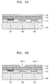
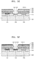
- FIGS. 4A through 4G illustrate cross-sectional views for explaining a first process of the organic light-emitting display apparatus of FIG. 1 ;
- FIGS. 5A through 5G illustrate cross-sectional views for explaining a second process of the organic light-emitting display apparatus of FIG. 1 ;
- FIGS. 6A through 6G illustrate cross-sectional views for explaining a third process of the organic light-emitting display apparatus of FIG. 1 ;
- FIGS. 7A through 7D illustrate cross-sectional views for explaining some processes of an organic light-emitting display apparatus according to a comparative example
- FIG. 8 illustrates a view for comparing sizes of emission areas of the organic light-emitting display apparatus of FIG. 1 and the organic light-emitting display apparatus according to the comparative example
- FIG. 9 illustrates a cross-sectional view of an organic light-emitting display apparatus according to another embodiment
- FIG. 10 illustrates a graph showing a relationship between a reflectance and a wavelength of each of pure silver (Ag) and a silver alloy.
- FIGS. 11A and 11B illustrate views illustrating particle defect patterns according to whether a first anode lower electrode includes silver.
- the term “and/or” includes any and all combinations of one or more of the associated listed items. Expressions such as “at least one of” when preceding a list of elements, modify the entire list of elements and do not modify the individual elements of the list.
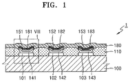
- FIG. 1 is a cross-sectional view of an organic light-emitting display apparatus 1 according to an embodiment.
- a plurality of anode lower electrodes including a first anode lower electrode 101 , a second anode lower electrode 102 , and a third anode lower electrode 103 are located on a substrate 100 to be spaced apart from one another.
- a pixel-defining film 110 covers ends of the first through third anode lower electrodes 101 , 102 , and 103 .
- First through third anode upper electrodes 141 , 142 , and 143 are respectively located on the first through third anode lower electrodes 101 , 102 , and 103 .
- First through third organic functional layers 151 , 152 , and 153 are respectively located on the first through third anode upper electrodes 141 , 142 , and 143 .
- First through third auxiliary cathodes 181 , 182 , and 183 are respectively located on the first through third organic functional layers 151 , 152 , and 153 .
- An integrated cathode 180 is located as a common electrode on the first through third auxiliary cathodes 181 , 182 , and 183 and the pixel-defining film 110 .
- FIG. 2 is a cross-sectional view for explaining a method of manufacturing the organic light-emitting display apparatus 1 according to the present example embodiment and the organic light-emitting display apparatus manufactured by using the method will now be explained in more detail with reference to FIGS. 2 through 6G .
- FIG. 2 is a cross-sectional view illustrating the first through third anode lower electrodes 101 , 102 , and 103 formed on the substrate 100 of the organic light-emitting display apparatus 1 according to the present example embodiment.
- FIG. 3 is a cross-sectional view illustrating the pixel-defining film 110 formed in the organic light-emitting display apparatus 1 according to the present example embodiment.
- FIGS. 4A through 4G are cross-sectional views for explaining a first process of the organic light-emitting display apparatus 1 according to the present example embodiment.
- FIGS. 5A through 5G are cross-sectional views for explaining a second process of the organic light-emitting display apparatus 1 according to the present example embodiment.
- FIGS. 6A through 6G are cross-sectional views for explaining a third process of the organic light-emitting display apparatus 1 according to the present example embodiment.
- a plurality of anode lower electrodes including the first anode lower electrode 101 , the second anode lower electrode 102 , and the third anode lower electrode 103 , is formed on the substrate 100 .
- the substrate 100 may be formed by using various materials.
- the substrate 100 may be formed of glass or plastic.
- the plastic may include materials having excellent heat resistance and excellent durability such as polyimide, polyethylenenaphthalate, polyethyleneterephthalate, polyarylate, polycarbonate, polyetherimide, and polyethersulfone.
- a buffer layer for planarizing a surface and preventing penetration of impurity elements may be formed over the substrate 100 .
- the buffer layer may have a single-layer structure or a multi-layer structure formed of silicon nitride and/or silicon oxide.
- Each of the first through third anode lower electrodes 101 , 102 , and 103 may be hole injection electrodes and may be formed of, for example, a material having a high work function.
- Each of the first through third anode lower electrodes 101 , 102 , and 103 may include, for example, a transparent conductive oxide component.
- each of the first through third anode lower electrodes 101 , 102 , and 103 may include at least one selected from the group of indium tin oxide, indium zinc oxide, zinc oxide, indium oxide, indium gallium oxide, and aluminum zinc oxide.
- Each of the first through third anode lower electrodes 101 , 102 , and 103 may include a metal component such as aluminum, magnesium, lithium, or calcium.
- each of the first through third anode lower electrodes 101 , 102 , and 103 does not include a silver (Ag) component that is a metal with a high reducibility. Since each of the first through third anode lower electrodes 101 , 102 , and 103 does not include a silver component, particle defects due to re-precipitation of silver may be avoided, which will be explained below in detail.
- a silver (Ag) component that is a metal with a high reducibility
- first through third anode lower electrodes 101 , 102 , and 103 may be respectively electrically connected to first through third thin-film transistors located between the substrate 100 and the first through third anode lower electrodes 101 , 102 , and 103 .
- the pixel-defining film 110 surrounding edges of the first anode lower electrode 101 , the second anode lower electrode 102 , and the third anode lower electrode 103 is formed on the substrate 100 .
- Ends of the first through third anode lower electrodes 101 , 102 , and 103 may be sharp.
- an electric field may concentrate on the ends of the first through third anode lower electrodes 101 , 102 , and 103 and an electrical short circuit may occur during operation.
- the first through third organic functional layers 151 , 152 , and 153 cover the ends of the first through third anode lower electrodes 101 , 102 , and 103 and a pixel-defining film 110 also covers the ends of the first through third anode lower electrodes 101 , 102 , and 103 .
- an electric field may be prevented from concentrating at the ends of the first through third anode lower electrodes 101 , 102 , and 103 .
- the pixel-defining film 110 may be an organic insulating film including, for example, a general-purpose polymer such as poly(methyl methacrylate) (PMMA) or polystyrene (PS), a polymer derivative having a phenol group, an acryl-based polymer, an imide-based polymer, an arylether-based polymer, an amide-based polymer, a fluorine-based polymer, a p-xylene-based polymer, a vinyl alcohol-based polymer, and a blend thereof.
- PMMA poly(methyl methacrylate)
- PS polystyrene
- a first lift-off layer 121 and a first photoresist 131 each including a fluoropolymer are sequentially formed on the substrate 100 on which the first through third anode lower electrodes 101 , 102 , and 103 are formed.
- the fluoropolymer included in the first lift-off layer 121 may include, for example, a polymer having a fluorine content ranging from about 20 wt % to about 60 wt %.
- the fluoropolymer included in the first lift-off layer 121 may include at least one from among a copolymer of polytetrafluoroethylene, polychlorotrifluoroethylene, polydichlorodifluoroethylene, chlorotrifluoroethylene, and dichlorofluoroethylene, a copolymer of tetrafluoroethylene and perfluoroalkylvinylether, a copolymer of chlorotrifluoroethylene and perfluoroalkylvinylether, a copolymer of tetrafluoroethylene and perfluoroalkylvinylether, and a copolymer of chlorotrifluoroethylene and perfluoroalkylvinylether.
- the first lift-off layer 121 may be formed on the substrate 100 by using, for example, a coating method, a printing method, or a deposition method.
- a coating method for example, curing and polymerization may be performed and then a process of forming a photoresist may be performed.
- a thickness of the first lift-off layer 121 may be, for example, equal to or greater than 0.2 ⁇ m and equal to or less than 5 ⁇ m.
- a time taken to dissolve the first lift-off layer 121 for patterning may be increased and thus a manufacturing process time may be increased.
- the first lift-off layer 121 is thinner, it may be difficult to perform a lift-off process.
- the first lift-off layer 121 may further include a moisture-absorbing agent.
- the moisture-absorbing agent may include various materials.
- the moisture-absorbing agent may include a material that is a compound in which metals are connected by oxygen such as calcium oxide, barium oxide, aluminum oxide, or magnesium oxide and that forms metal hydroxide by reacting with water.
- the moisture-absorbing agent may include any one selected from the group of a metal halide, an inorganic acid salt of a metal, an organic acid salt, a porous inorganic compound, and a combination thereof.
- the moisture-absorbing agent may include an acryl-based organic material, a methacryl-based organic material, a polyisoprene-based organic material, a vinyl-based organic material, an epoxy-based organic material, a urethane-based organic material, or a cellulose-based organic material.
- the moisture-absorbing agent may include a titania-based inorganic material, a silicon oxide-based inorganic material, a zirconia-based inorganic material, or an alumina-based inorganic material.
- the moisture-absorbing agent may include a sealant formed of epoxy silane, vinyl silane, amine silane, or methacrylate silane.
- the moisture-absorbing agent may trap moisture generated during a first process and may prevent degradation of the first organic functional layer 151 formed in the first process.
- the first photoresist 131 is formed on the first lift-off layer 121 .
- the first photoresist 131 may be exposed and developed by using a first photomask.
- the first photoresist 131 may be a positive photoresist or a negative photoresist. In the present example embodiment, it is assumed that the first photoresist 131 is a positive photoresist.
- the first photoresist 131 is patterned.
- the first photoresist 131 that is exposed and developed is removed at a first portion 131 - 1 corresponding to the first anode lower electrode 101 and remains at a second portion 131 - 2 other than the first portion 131 - 1 .
- the first lift-off layer 121 is etched by using a pattern of the first photoresist 131 of FIG. 4B as an etch mask.
- the etchant may include a solvent to etch the fluoropolymer.
- the etchant may include a first solvent including fluorine.
- the first solvent may include hydrofluoroether.
- Hydrofluoroether is a material that is electrochemically stable due to a low interaction with other materials and is environmentally stable due to a low global warming potential and a low toxicity.
- a portion of the first lift-off layer 121 formed over the first anode lower electrode 101 to correspond to the first portion 131 - 1 is etched during an etching process.
- the first lift-off layer 121 may be etched to form a first undercut profile UC 1 under a boundary surface of the first portion 131 - 1 of the first photoresist 131 and to be spaced apart by a predetermined interval from a side surface of the first anode lower electrode 101 .
- the first undercut profile UC 1 may allow the first anode upper electrode 141 to cover an inclined surface that is an end of the pixel-defining film 110 in a subsequent deposition process.
- the first anode upper electrode 141 is formed on a structure of FIG. 4C .
- the first anode upper electrode 141 may include various metals.
- the first anode upper electrode 141 may include, for example, a material with a reducibility higher than a material of the first anode lower electrode 101 .
- the first anode upper electrode 141 may include silver with a high reducibility.
- Silver that is a metal with a high reflectance may be used as a material of a reflective electrode of a display apparatus.
- an electrode close to the substrate 100 may be a reflective electrode.
- silver ions receiving electrons in an etching process for forming a pattern of the first anode lower electrode 101 may be re-precipitated to form particles, thereby leading to defects.
- the first anode lower electrode 101 does not include a silver component and the first anode upper electrode 141 includes a silver component.
- particle defects of a display apparatus may be reduced, a reflectance may be increased, and light efficiency may be improved.
- the first anode lower electrode 101 may be subjected to an etching process in order to form a pattern.
- the first anode upper electrode 141 of the present example embodiment may be formed by using a vacuum deposition method without undergoing an etching process.
- a part of the first anode upper electrode 141 may be deposited to directly contact a top surface of the first anode lower electrode 101 and a part of the first anode upper electrode 141 may be deposited to contact the inclined surface that is the end of the pixel-defining film 110 , by using the first lift-off layer 121 and the first photoresist 131 as masks. Accordingly, an emission area may be increased and defects due to a residue generated in a subsequent lift-off process may be reduced.
- the first organic functional layer 151 is formed on a structure of FIG. 4D .
- the first organic functional layer 151 includes a first organic emission layer. Also, the first organic functional layer 151 may further include at least one functional layer from among a hole injection layer, a hole transport layer, an electron transport layer, and an electron injection layer.
- the first organic functional layer 151 may be formed by using a vacuum deposition method, like the first anode upper electrode 141 .
- the first lift-off layer 121 and the first photoresist 131 function as deposition masks.
- a part of the first organic functional layer 151 is formed to cover a top surface of the first anode upper electrode 141 and another part of the first organic functional layer 151 is formed on the second portion 131 - 2 of the first photoresist 131 .
- the first auxiliary cathode 181 is formed on a structure of FIG. 4E .
- the first auxiliary cathode 181 may be formed by using, for example, a vacuum deposition method, e.g., like the first anode upper electrode 141 and the first organic functional layer 151 .
- a vacuum deposition method e.g., like the first anode upper electrode 141 and the first organic functional layer 151 .
- the first lift-off layer 121 and the first photoresist 131 may function as deposition masks.
- a part of the first auxiliary cathode 181 is formed to cover a top surface of the first organic functional layer 151 and another part of the first auxiliary cathode 181 is formed on the second portion 131 - 2 of the first photoresist 131 other than the first portion 131 - 1 .
- the first auxiliary cathode 181 may include the same material as that of the cathode 180 that is a common electrode. In another implementation, the first auxiliary cathode 181 may be formed of a material different from that of the cathode 180 . The first auxiliary cathode 181 may function as a barrier for protecting the first organic functional layer 151 from a solvent used in a subsequent lift-off process.
- a lift-off process is performed on a structure of FIG. 4F .
- the first lift-off layer 121 may include the fluoropolymer, and a second solvent including fluorine may be used in the lift-off process.
- the first organic functional layer 151 may be formed and then the lift-off process may be performed.
- the second solvent may include a material having a low reactivity with the first organic functional layer 151 .
- the second solvent may include, for example, hydrofluoroether, like the first solvent.
- a second process of forming the second organic functional layer 152 (see FIG. 5G ) (which may emit light of a color different from that of the first organic functional layer 151 ) may be performed on an area where the second anode lower electrode 102 is located.
- a second lift-off layer 122 and a second photoresist 132 which may each include a fluoropolymer, are sequentially formed on the substrate 100 on which the first through third anode lower electrodes 101 , 102 , and 103 and the first organic functional layer 151 are formed.
- the second lift-off layer 122 may be formed by using, for example, a coating method, a printing method, or a deposition method.
- the second lift-off layer 122 may be formed of the same material as that of the first lift-off layer 121 .
- the second photoresist 132 may be exposed and developed by using a second photomask.
- the second photoresist 132 may be, for example, a positive photoresist or a negative photoresist. In the present example embodiment, the second photoresist is described as a positive photoresist.
- the second photoresist 132 is patterned.
- the second photoresist 132 that is exposed and developed is removed at a first portion 132 - 1 corresponding to the second anode lower electrode 102 and remains at a second portion 132 - 2 other than the first portion 132 - 1 .
- the second lift-off layer 122 is etched by using a pattern of the second photoresist 132 of FIG. 5B as an etch mask.
- the second lift-off layer 122 may includes the fluoropolymer, and the etchant may include a solvent that may etch the fluoropolymer.
- the etchant may include a first solvent including fluorine.
- the first solvent may include hydrofluoroether, like in the first process.
- the first solvent may include a material different from that in the first process.
- a portion of the second lift-off layer 122 formed over the second anode lower electrode 102 to correspond to the first portion 132 - 1 is etched during an etching process.
- the second lift-off layer 122 may be etched to form a second undercut profile UC 2 under a boundary surface of the first portion 132 - 1 of the second photoresist 132 and to be spaced apart by a predetermined interval from a side surface of the second anode lower electrode 102 .
- the second undercut profile UC 2 may allow the second anode upper electrode 142 to cover an inclined surface that is an end of the pixel-defining film 110 in a subsequent deposition process.
- the second anode upper electrode 142 is formed on a structure of FIG. 5C .
- the second anode upper electrode 142 may include, for example, various metals.
- the second anode upper electrode 142 may include a material that is the same as or different from that of the first anode upper electrode 141 .
- the second anode upper electrode 142 may include a material with a reducibility higher than that of the second anode lower electrode 102 .
- the second anode upper electrode 142 may include silver with a high reducibility.
- a part of the second anode upper electrode 142 may be deposited to directly contact a top surface of the second anode lower electrode 102 , and a part of the second anode upper electrode 142 may be deposited to contact the inclined surface that is the end of the pixel-defining film 110 , using the second lift-off layer 122 and the second photoresist 132 as masks. Accordingly, an emission area may be increased and defects due to a residue generated in a subsequent lift-off process may be reduced.
- the second organic functional layer 152 is formed on a structure of FIG. 5D .
- the second organic functional layer 152 includes a second organic emission layer. Also, the second organic functional layer 152 may further include at least one functional layer from among a hole injection layer, a hole transport layer, an electron transport layer, and an electron injection layer.
- the second organic functional layer 152 may be formed by using, for example, a vacuum deposition method, like the second anode upper electrode 142 .
- the second lift-off layer 122 and the second photoresist 132 may function as deposition masks.
- a part of the second organic functional layer 152 is formed to cover a top surface of the second anode upper electrode 142 and another part of the second organic functional layer 152 is formed on the second portion 132 - 2 of the second photoresist 132 .
- the second auxiliary cathode 182 is formed on a structure of FIG. 5E .
- the second auxiliary cathode 182 may be formed by using, for example, a vacuum deposition method, like the second anode upper electrode 142 and the second organic functional layer 152 .
- the second lift-off layer 122 and the second photoresist 132 may function as deposition masks.
- a part of the second auxiliary cathode 182 is formed to cover a top surface of the second organic functional layer 152 and another part of the second auxiliary cathode 182 is formed on the second portion 132 - 2 of the second photoresist 132 other than the first portion 132 - 1 .
- the second auxiliary cathode 182 may include a material that is the same as or different from that of the first auxiliary cathode 181 .
- the second auxiliary cathode 182 may include the same material as that of the cathode 180 that is a common electrode.
- the second auxiliary cathode 182 may be formed of a material different from that of the cathode 180 .
- the second auxiliary cathode 182 may function as a barrier for protecting the second organic functional layer 152 from a solvent used in a subsequent lift-off process.
- a lift-off process is performed on a structure of FIG. 5F .
- the second lift-off layer 122 may include the fluoropolymer, and a second solvent including fluorine may be used in the lift-off process. Since the second organic functional layer 152 may be formed and then the lift-off process may be performed, the second solvent may include a material having a low reactivity with the second organic functional layer 152 .
- the second solvent may include, for example, hydrofluoroether, like the first solvent.
- a third process of forming the third organic functional layer 153 (see FIG. 6G ) (which may emit light of a color different from those of the first organic functional layer 151 and the second organic functional layer 152 ) may be performed on an area where the third anode lower electrode 103 is located.
- a third lift-off layer 123 and a third photoresist 333 which may each include a fluoropolymer, are sequentially formed on the substrate 100 on which the first through third anode lower electrodes 101 , 102 , and 103 and the first and second organic functional layers 151 and 152 are formed.
- the third lift-off layer 123 may be formed by using, for example, a coating method, a printing method, and a deposition method.
- the third lift-off layer 123 may be formed of the same material as those/that of the first and/or the second lift-off layers 121 and 122 .
- the third photoresist 133 may be exposed and developed by using a third photomask.
- the third photoresist 133 may be a positive photoresist or a negative photoresist. In the present example embodiment, the third photoresist is described as a positive photoresist.
- the third photoresist 133 is patterned.
- the third photoresist 133 is exposed and developed to be removed at a first portion 133 - 1 corresponding to the third anode lower electrode 103 and to remain at a second portion 133 - 2 other than the first portion 133 - 1 .
- the third lift-off layer 123 may be etched by using a pattern of the third photoresist 133 of FIG. 6B as an etch mask.
- the third lift-off layer 123 may include the fluoropolymer, and the etchant may include a solvent that etches the fluoropolymer.
- the etchant may include a first solvent including fluorine.
- the first solvent may include, for example, hydrofluoroether, like in the first and second processes.
- the first solvent may include a material different from that in the first and second processes.
- a portion of the third lift-off layer 123 formed over the third anode lower electrode 103 to correspond to the first portion 133 - 1 is etched during an etching process.
- the third lift-off layer 123 may be etched to form a third undercut profile UC 3 under a boundary surface of the first portion 133 - 1 of the third photoresist 133 and to be spaced apart by a predetermined interval from a side surface of the third anode lower electrode 103 .
- the third undercut profile UC 3 may allow the third anode upper electrode 143 to cover an inclined surface that is an end of the pixel-defining film 110 in a subsequent deposition process.
- the third anode upper electrode 143 is formed on a structure of FIG. 6C .
- the third anode upper electrode 143 may include various metals.
- the third anode upper electrode 143 may include a material that is the same as or different from those of the first and second anode upper electrodes 141 and 142 .
- the third anode upper electrode 143 may include a material with a reducibility higher than that of the third anode lower electrode 103 .
- the third anode upper electrode 143 may include silver with a high reducibility.
- a part of the third anode upper electrode 143 may be deposited to directly contact a top surface of the third anode lower electrode 103 and a part of the third anode upper electrode 143 may be deposited to contact the inclined surface that is the end of the pixel-defining film 110 , using the third lift-off layer 123 and the third photoresist 133 as masks. Accordingly, an emission area may be increased and defects due to a residue generated in a subsequent lift-off process may be reduced.
- the third organic functional layer 153 is formed on a structure of FIG. 6D .
- the third organic functional layer 153 includes a third organic emission layer. Also, the third organic functional layer 153 may further include at least one functional layer from among a hole injection layer, a hole transport layer, an electron transport layer, and an electron injection layer.
- the third organic functional layer 153 may be formed by using, for example, a vacuum deposition process, like the third anode upper electrode 143 .
- a vacuum deposition process the third lift-off layer 123 and the third photoresist 133 function as deposition masks.
- a part of the third organic functional layer 153 is formed to cover a top surface of the third anode upper electrode 143 and another part of the third organic functional layer 153 is formed on the second portion 133 - 2 of the third photoresist 133 .
- the third auxiliary cathode 183 is formed on a structure of FIG. 6E .
- the third auxiliary cathode 183 may be formed by using, for example, a vacuum deposition method, like the third anode upper electrode 143 and the third organic functional layer 153 .
- the third lift-off layer 123 and the third photoresist 133 function as deposition masks.
- a part of the third auxiliary cathode 183 is formed to cover a top surface of the third organic functional layer 153 and another part of the third auxiliary cathode 183 is formed on the second portion 133 - 2 of the third photoresist 133 other than the first portion 133 - 1 .
- the third auxiliary cathode 183 may include a material that is the same as or different from those of the first and second auxiliary cathodes 181 and 182 .
- the third auxiliary cathode 183 may include the same material as that of the cathode 180 that is a common electrode.
- the third auxiliary cathode 183 may be formed of a material different from that of the cathode 180 .
- the third auxiliary cathode 183 may function as a barrier for protecting the third organic functional layer 153 from a solvent used in a subsequent lift-off process.
- a lift-off process is performed on a structure of FIG. 6F .
- the third lift-off layer 123 may include the fluoropolymer, and a second solvent including fluorine may be used in the lift-off process. Since the third organic functional layer 153 may be formed and then the lift-off process may be performed, the second solvent may include a material having a low reactivity with the third organic functional layer 153 .
- the second solvent may include, for example, hydrofluoroether, like the first solvent.
- the first through third organic functional layers 151 , 152 , and 153 may emit light of different colors. White light may be formed by mixing light emitted from the first through third organic functional layers 151 , 152 , and 153 .
- the first through third organic functional layers 151 , 152 , and 153 may respectively emit red light, green light, and blue light.
- the first through third organic functional layers 151 , 152 , and 153 may correspond to subpixels constituting a unit pixel of the organic light-emitting display apparatus 1 .
- the organic light-emitting display apparatus 1 of FIG. 1 may include one unit pixel. Also, the present example embodiment may be applied to an organic light-emitting display apparatus including a plurality of the unit pixels of FIG. 1 .
- a plurality of the first organic functional layers 151 that emit light of a first color may be simultaneously formed.
- a plurality of the second organic functional layers 152 that emit light of a second color may be simultaneously formed.
- a plurality of the third organic functional layers 153 that emit light of a third color may be simultaneously formed. Light of full colors may be formed by using the first through third processes.
- the cathode 180 is formed on a structure of FIG. 6G .
- the cathode 180 may be integrally formed as a common electrode on the first through third organic functional layers 151 , 152 , and 153 and the pixel-defining film 110 .
- first through third anode lower electrodes 101 , 102 , and 103 and the first through third anode upper electrodes 141 , 142 , and 143 are hole injection electrodes and the first through third auxiliary cathodes 181 , 182 , and 183 and the cathode 180 are electron injection electrodes in the present example embodiment
- the present disclosure is not limited thereto and electron injection electrodes may be formed on an area where the first through third anode lower electrodes 101 , 102 , and 103 and the first through third anode upper electrodes 141 , 142 , and 143 are located and hole injection electrodes may be formed on an area where the first through third auxiliary cathodes 181 , 182 , and 183 , and the cathode 180 are located.
- patterns of the first through third organic functional layers 151 , 152 , and 153 may be formed by using first through third lift-off processes. Thus, issues relating to the use of the metal mask may be avoided.
- FIGS. 7A through 7D are cross-sectional views for explaining some processes of an organic light-emitting display apparatus 2 according to a comparative example.
- the pixel-defining film 110 that covers ends of the first through third anode lower electrodes 101 , 102 , and 103 formed on the substrate 100 to be spaced apart from one another is formed.
- the first lift-off layer 121 and the first photoresist 131 are sequentially stacked, and the first photoresist 131 is patterned through exposure and development.
- the first photoresist 131 is removed at the first portion 131 - 1 corresponding to the first anode lower electrode 101 and remains at the second portion 131 - 2 other than the first portion 131 - 1 .
- the first undercut profile UC 1 is formed under a boundary surface of the first portion 131 - 1 of the first photoresist 131 by etching the first lift-off layer 121 by using a pattern of the first photoresist 131 as an etch mask. A portion of the first lift-off layer 121 formed over the first anode lower electrode 101 to correspond to the first portion 131 - 1 is etched. The first lift-off layer 121 including a fluoropolymer may not be completely removed and a residue P 1 may remain on the first anode lower electrode 101 as shown in FIG. 7A .
- the first organic functional layer 151 and the first auxiliary cathode 181 are deposited on a structure of FIG. 7A .
- a lift-off process is performed on a structure of FIG. 7B .
- the first lift-off layer 121 including the fluoropolymer may not be completely removed and a residue P 2 may remain on the second anode lower electrode 102 as shown in FIG. 7C .
- the residue P 1 on the first anode lower electrode 101 and the residue P 2 on the second anode lower electrode 102 may degrade hole or electron injection characteristics from an electrode to an organic functional layer.
- the first through third anode upper electrodes 141 , 142 , and 143 may be formed by using a deposition process using a lift-off layer on the first through third anode lower electrodes 101 , 102 , and 103 .
- the residues may not directly contact the first through third organic functional layers 151 , 152 , and 153 . Accordingly, according to an example embodiment, defects due to a residue generated in a lift-off process may be reduced.
- FIG. 7D is a cross-sectional view of the organic light-emitting display apparatus 2 according to the comparative example after first through third processes are completed.
- FIG. 8 is a view for comparing sizes of emission areas of the organic light-emitting display apparatus 1 according to the present example embodiment and the organic light-emitting display apparatus 2 according to the comparative example.
- an emission area EA 2 is defined as a portion of the first anode lower electrode 101 that is not covered by the pixel-defining film 110 .
- the first anode upper electrode 141 is formed on a top surface of the first anode lower electrode 101 and on an inclined surface that is an end of the pixel-defining film 110 and then the first organic functional layer 151 is formed on the first anode upper electrode 141 .
- an emission area EA 1 is greater than the emission area EA 2 of the comparative example. Accordingly, an aperture ratio of a display apparatus may be increased.
- FIG. 9 is a cross-sectional view of an organic light-emitting display apparatus 3 according to another example embodiment.
- the organic light-emitting display apparatus 3 of FIG. 9 is different from the organic light-emitting display apparatus 1 in that specific materials are selected as materials of the first anode lower electrode 103 and the first anode upper electrode 141 .
- the first anode lower electrode 103 is formed of indium tin oxide and the first anode upper electrode 141 is formed of silver.
- the first anode lower electrode 103 has a stacked structure formed of aluminum (Al) and indium tin oxide, and the first anode upper electrode 141 is formed of silver Ag.
- Silver is a metal with a high reducibility.
- silver ions receiving electrons in an etching process for forming a pattern of the first anode lower electrode 101 may be re-precipitated to form particles, thereby leading to defects.
- FIGS. 11A and 11B are views illustrating particle defect patterns according to whether the first anode lower electrode 101 includes silver.
- FIG. 11A illustrates a result obtained after a lift-off process is performed when the first anode lower electrode 101 does not include silver.
- FIG. 11B illustrates a result obtained after a lift-off process is performed when the first anode lower electrode 101 includes silver.
- the first anode upper electrode 141 is formed in a vacuum deposition process and the first anode upper electrode 141 is blocked from external air in a subsequent encapsulation process.
- the first anode upper electrode 141 may be formed of pure silver, instead of an alloy.
- FIG. 10 is a graph showing a relationship between a reflectance and a wavelength of each of pure silver and a silver alloy. Since the pure silver has a light reflectance higher than that of the silver alloy and an increase in a reflectance in blue wavelengths equal to or less than 500 nm is large, the efficiency of a blue device may be improved.
- each of the organic light-emitting display apparatuses may further include an encapsulation member that encapsulates an organic emission layer.
- the encapsulation member may include a glass substrate, a metal foil, and a thin-film encapsulation layer in which an inorganic layer and an organic layer are combined.
- embodiments may provide an organic light-emitting display apparatus that may reduce defects and manufacturing costs, and a method of manufacturing the organic light-emitting display apparatus.
- an emission layer may be formed without using a fine metal mask (FMM), and a high resolution display panel may be formed.
- FMM fine metal mask
- an anode upper electrode may be deposited in a vacuum.
- defects due to a residue formed in a lift-off process may be reduced.
- an anode upper electrode may be deposited to extend to an inclined surface of a pixel-defining film.
- an emission area may be increased and an aperture ratio of a display apparatus may be increased.
- an anode lower electrode may not include silver. Thus, particle defects due to silver may be avoided.
Landscapes
- Engineering & Computer Science (AREA)
- Physics & Mathematics (AREA)
- Manufacturing & Machinery (AREA)
- Optics & Photonics (AREA)
- Microelectronics & Electronic Packaging (AREA)
- Geometry (AREA)
- Electroluminescent Light Sources (AREA)
Abstract
Description
Claims (17)
Applications Claiming Priority (2)
| Application Number | Priority Date | Filing Date | Title |
|---|---|---|---|
| KR10-2016-0098043 | 2016-08-01 | ||
| KR1020160098043A KR102603867B1 (en) | 2016-08-01 | 2016-08-01 | Organic light-emitting apparatus and the method for manufacturing of the organic light-emitting display apparatus |
Publications (2)
| Publication Number | Publication Date |
|---|---|
| US20180033968A1 US20180033968A1 (en) | 2018-02-01 |
| US10693068B2 true US10693068B2 (en) | 2020-06-23 |
Family
ID=61010174
Family Applications (1)
| Application Number | Title | Priority Date | Filing Date |
|---|---|---|---|
| US15/657,439 Active US10693068B2 (en) | 2016-08-01 | 2017-07-24 | Organic light-emitting display apparatus and method of manufacturing the same |
Country Status (3)
| Country | Link |
|---|---|
| US (1) | US10693068B2 (en) |
| KR (1) | KR102603867B1 (en) |
| CN (1) | CN107680985B (en) |
Cited By (4)
| Publication number | Priority date | Publication date | Assignee | Title |
|---|---|---|---|---|
| US20200161391A1 (en) * | 2017-08-30 | 2020-05-21 | Boe Technology Group Co., Ltd | Pixel defining layer and method for manufacturing the same, display panel and method for manufacturing the same, and display device |
| US11659747B2 (en) | 2020-04-23 | 2023-05-23 | Seeya Optronics Co., Ltd. | Display apparatus including an uneven structure, and method of manufacturing the same |
| US12274116B2 (en) | 2018-04-24 | 2025-04-08 | Samsung Display Co., Ltd. | Organic light-emitting display apparatus and method of manufacturing the same |
| US12356846B2 (en) | 2018-12-17 | 2025-07-08 | Samsung Display Co., Ltd. | Organic light-emitting display device, and method for manufacturing organic light-emitting display device |
Families Citing this family (18)
| Publication number | Priority date | Publication date | Assignee | Title |
|---|---|---|---|---|
| KR102603867B1 (en) * | 2016-08-01 | 2023-11-21 | 삼성디스플레이 주식회사 | Organic light-emitting apparatus and the method for manufacturing of the organic light-emitting display apparatus |
| KR102278608B1 (en) * | 2017-03-10 | 2021-07-19 | 삼성디스플레이 주식회사 | Organic light-emitting apparatus and the method for manufacturing of the organic light-emitting display apparatus |
| KR102482456B1 (en) * | 2017-03-13 | 2022-12-29 | 삼성디스플레이 주식회사 | Organic light-emitting apparatus and the method for manufacturing of the organic light-emitting display apparatus |
| CN109103215B (en) * | 2017-06-21 | 2021-03-09 | 京东方科技集团股份有限公司 | Organic light emitting diode display panel, manufacturing method thereof and display device |
| US10700299B2 (en) * | 2017-08-01 | 2020-06-30 | Zixu Optronics Technology (Shanghai) Limited | Method for manufacturing organic light emitting diode using conductive protective layer |
| CN108321183B (en) * | 2018-03-30 | 2021-03-19 | 武汉天马微电子有限公司 | An organic light-emitting display panel and display device |
| KR102615115B1 (en) * | 2018-05-11 | 2023-12-19 | 삼성디스플레이 주식회사 | Display device |
| CN109052310B (en) * | 2018-07-06 | 2021-07-23 | 中国工程物理研究院电子工程研究所 | Method for preparing partially covered side electrode |
| US20200058715A1 (en) * | 2018-08-16 | 2020-02-20 | Int Tech Co., Ltd. | Light emitting device and manufacturing method thereof |
| KR102614588B1 (en) | 2018-08-20 | 2023-12-18 | 삼성디스플레이 주식회사 | Method of manufacturing display apparatus |
| KR102588594B1 (en) * | 2018-10-16 | 2023-10-16 | 삼성디스플레이 주식회사 | Display apparatus and manufacturing method thereof |
| CN113169217A (en) * | 2018-11-19 | 2021-07-23 | 陈鼎国 | Organic light-emitting display device and method of making the same |
| CN109860239B (en) * | 2018-12-13 | 2021-03-16 | 武汉华星光电半导体显示技术有限公司 | Array substrate, manufacturing method thereof and display device |
| KR102682395B1 (en) * | 2018-12-26 | 2024-07-09 | 삼성디스플레이 주식회사 | Organic light emitting display apparatus and method of manufacturing the same |
| KR102654917B1 (en) | 2019-04-15 | 2024-04-05 | 삼성디스플레이 주식회사 | Organic light emitting display apparatus and method of manufacturing the same |
| CN110323356B (en) * | 2019-05-08 | 2021-11-02 | 京东方科技集团股份有限公司 | OLED display substrate, manufacturing method, and display device |
| KR102741000B1 (en) | 2019-06-26 | 2024-12-12 | 삼성디스플레이 주식회사 | Display apparatus and manufacturing the same |
| CN113451529B (en) * | 2021-06-29 | 2024-07-19 | 京东方科技集团股份有限公司 | Display panel, manufacturing method and display device |
Citations (21)
| Publication number | Priority date | Publication date | Assignee | Title |
|---|---|---|---|---|
| JPH10261490A (en) | 1997-03-18 | 1998-09-29 | Idemitsu Kosan Co Ltd | Organic EL display device and manufacturing method thereof |
| JP2002170669A (en) | 2000-12-01 | 2002-06-14 | Tdk Corp | Organic EL display device and manufacturing method thereof |
| US20060238111A1 (en) | 2005-04-22 | 2006-10-26 | Masao Shimizu | Organic light emitting display apparatus |
| WO2008038588A1 (en) | 2006-09-28 | 2008-04-03 | Rohm Co., Ltd. | Method for manufacturing organic material apparatus |
| US20120181554A1 (en) | 2007-11-20 | 2012-07-19 | Irving Lyn M | Multicolored mask process for making display circuitry |
| US20130038203A1 (en) * | 2011-08-12 | 2013-02-14 | Young-Il Kim | Organic light-emitting device and method of manufacturing the same |
| US20130069067A1 (en) * | 2011-09-20 | 2013-03-21 | Keun Chun Youn | Organic light emitting diode (oled) display device and method for manufacturing the same |
| US8772762B2 (en) * | 2009-03-25 | 2014-07-08 | Toppan Printing Co., Ltd. | Organic electroluminescent device, method for manufacturing organic electroluminescent device, image display device, and method for manufacturing image display device |
| US20140239262A1 (en) * | 2013-02-25 | 2014-08-28 | Samsung Display Co., Ltd. | Organic light-emitting display device and method of manufacturing the same |
| US9076993B2 (en) * | 2012-12-27 | 2015-07-07 | Lg Display Co., Ltd. | Organic light emitting display device and method for manufacturing the same |
| US20160126489A1 (en) * | 2013-07-04 | 2016-05-05 | Joled Inc. | Light-emitting element, display device, and method for manufacturing light-emitting element |
| US20170117506A1 (en) * | 2014-06-12 | 2017-04-27 | Joled Inc. | Method for manufacturing display panel |
| US20170222190A1 (en) * | 2016-02-02 | 2017-08-03 | Samsung Display Co., Ltd. | Organic light-emitting apparatus and method of manufacturing the same |
| US20170250344A1 (en) * | 2016-02-29 | 2017-08-31 | Samsung Display Co., Ltd | Organic light-emitting display apparatus and method of manufacturing the same |
| US20180033968A1 (en) * | 2016-08-01 | 2018-02-01 | Samsung Display Co., Ltd. | Organic light-emitting display apparatus and method of manufacturing the same |
| US20180033967A1 (en) * | 2016-07-29 | 2018-02-01 | Samsung Display Co., Ltd. | Organic light-emitting display apparatus and method of manufacturing the same |
| US20180047930A1 (en) * | 2016-08-12 | 2018-02-15 | Samsung Display Co., Ltd. | Organic light-emitting display apparatus and method of manufacturing the same |
| US9911795B2 (en) * | 2014-11-14 | 2018-03-06 | Boe Technology Group Co., Ltd. | Pixel unit and method of manufacturing the same, light emitting device and display device |
| US20180190907A1 (en) * | 2017-01-03 | 2018-07-05 | Samsung Display Co., Ltd. | Organic light-emitting display apparatus and method of manufacturing the same |
| US20190173046A1 (en) * | 2017-12-01 | 2019-06-06 | Samsung Display Co., Ltd. | Organic light-emitting apparatus and method of manufacturing the same |
| US20190207163A1 (en) * | 2017-12-29 | 2019-07-04 | Lg Display Co., Ltd. | Electroluminescence display device |
Family Cites Families (7)
| Publication number | Priority date | Publication date | Assignee | Title |
|---|---|---|---|---|
| US4519872A (en) * | 1984-06-11 | 1985-05-28 | International Business Machines Corporation | Use of depolymerizable polymers in the fabrication of lift-off structure for multilevel metal processes |
| JP2003187972A (en) * | 2001-12-20 | 2003-07-04 | Dainippon Printing Co Ltd | Method for manufacturing organic EL element and organic EL transfer member and transfer object |
| JP5995477B2 (en) * | 2011-04-27 | 2016-09-21 | キヤノン株式会社 | Manufacturing method of organic EL display device |
| US9502603B2 (en) * | 2011-05-12 | 2016-11-22 | Wavesquare Inc. | Vertically structured group III nitride semiconductor LED chip and method for manufacturing the same |
| KR20140120427A (en) * | 2013-04-02 | 2014-10-14 | 삼성디스플레이 주식회사 | Organic light emitting diode display and method for manufacturing organic light emitting diode display |
| CN110459677B (en) * | 2014-08-01 | 2022-11-22 | 正交公司 | Photolithographic patterning of organic electronic devices |
| EP3175497A4 (en) * | 2014-08-01 | 2018-11-21 | Orthogonal Inc. | Photolithographic patterning of devices |
-
2016
- 2016-08-01 KR KR1020160098043A patent/KR102603867B1/en active Active
-
2017
- 2017-07-24 US US15/657,439 patent/US10693068B2/en active Active
- 2017-07-31 CN CN201710638787.8A patent/CN107680985B/en active Active
Patent Citations (28)
| Publication number | Priority date | Publication date | Assignee | Title |
|---|---|---|---|---|
| JPH10261490A (en) | 1997-03-18 | 1998-09-29 | Idemitsu Kosan Co Ltd | Organic EL display device and manufacturing method thereof |
| JP2002170669A (en) | 2000-12-01 | 2002-06-14 | Tdk Corp | Organic EL display device and manufacturing method thereof |
| US7692375B2 (en) * | 2005-04-22 | 2010-04-06 | Hitachi Displays, Ltd. | Organic light emitting display apparatus |
| US20060238111A1 (en) | 2005-04-22 | 2006-10-26 | Masao Shimizu | Organic light emitting display apparatus |
| US7898172B2 (en) * | 2005-04-22 | 2011-03-01 | Hitachi Displays, Ltd. | Organic light emitting display apparatus |
| WO2008038588A1 (en) | 2006-09-28 | 2008-04-03 | Rohm Co., Ltd. | Method for manufacturing organic material apparatus |
| JP2008085200A (en) | 2006-09-28 | 2008-04-10 | Kyoto Univ | Manufacturing method of organic material device |
| US20120181554A1 (en) | 2007-11-20 | 2012-07-19 | Irving Lyn M | Multicolored mask process for making display circuitry |
| US8772762B2 (en) * | 2009-03-25 | 2014-07-08 | Toppan Printing Co., Ltd. | Organic electroluminescent device, method for manufacturing organic electroluminescent device, image display device, and method for manufacturing image display device |
| US20130038203A1 (en) * | 2011-08-12 | 2013-02-14 | Young-Il Kim | Organic light-emitting device and method of manufacturing the same |
| US8816579B2 (en) * | 2011-08-12 | 2014-08-26 | Samsung Display Co., Ltd. | Organic light-emitting device and method of manufacturing the same |
| US20130069067A1 (en) * | 2011-09-20 | 2013-03-21 | Keun Chun Youn | Organic light emitting diode (oled) display device and method for manufacturing the same |
| US9076993B2 (en) * | 2012-12-27 | 2015-07-07 | Lg Display Co., Ltd. | Organic light emitting display device and method for manufacturing the same |
| US20140239262A1 (en) * | 2013-02-25 | 2014-08-28 | Samsung Display Co., Ltd. | Organic light-emitting display device and method of manufacturing the same |
| US20160126489A1 (en) * | 2013-07-04 | 2016-05-05 | Joled Inc. | Light-emitting element, display device, and method for manufacturing light-emitting element |
| US9825250B2 (en) * | 2013-07-04 | 2017-11-21 | Joled Inc. | Light-emitting element, display device, and method for manufacturing light-emitting element |
| US20170117506A1 (en) * | 2014-06-12 | 2017-04-27 | Joled Inc. | Method for manufacturing display panel |
| US9911795B2 (en) * | 2014-11-14 | 2018-03-06 | Boe Technology Group Co., Ltd. | Pixel unit and method of manufacturing the same, light emitting device and display device |
| US20170222190A1 (en) * | 2016-02-02 | 2017-08-03 | Samsung Display Co., Ltd. | Organic light-emitting apparatus and method of manufacturing the same |
| US20170250344A1 (en) * | 2016-02-29 | 2017-08-31 | Samsung Display Co., Ltd | Organic light-emitting display apparatus and method of manufacturing the same |
| US20180033967A1 (en) * | 2016-07-29 | 2018-02-01 | Samsung Display Co., Ltd. | Organic light-emitting display apparatus and method of manufacturing the same |
| US20180033968A1 (en) * | 2016-08-01 | 2018-02-01 | Samsung Display Co., Ltd. | Organic light-emitting display apparatus and method of manufacturing the same |
| US20180047930A1 (en) * | 2016-08-12 | 2018-02-15 | Samsung Display Co., Ltd. | Organic light-emitting display apparatus and method of manufacturing the same |
| US20180190907A1 (en) * | 2017-01-03 | 2018-07-05 | Samsung Display Co., Ltd. | Organic light-emitting display apparatus and method of manufacturing the same |
| US10431742B2 (en) * | 2017-01-03 | 2019-10-01 | Samsung Display Co., Ltd. | Organic light-emitting display apparatus and method of manufacturing the same |
| US20190378986A1 (en) * | 2017-01-03 | 2019-12-12 | Samsung Display Co., Ltd. | Organic light-emitting display apparatus and method of manufacturing the same |
| US20190173046A1 (en) * | 2017-12-01 | 2019-06-06 | Samsung Display Co., Ltd. | Organic light-emitting apparatus and method of manufacturing the same |
| US20190207163A1 (en) * | 2017-12-29 | 2019-07-04 | Lg Display Co., Ltd. | Electroluminescence display device |
Cited By (5)
| Publication number | Priority date | Publication date | Assignee | Title |
|---|---|---|---|---|
| US20200161391A1 (en) * | 2017-08-30 | 2020-05-21 | Boe Technology Group Co., Ltd | Pixel defining layer and method for manufacturing the same, display panel and method for manufacturing the same, and display device |
| US10886343B2 (en) * | 2017-08-30 | 2021-01-05 | Boe Technology Group Co., Ltd. | Pixel defining layer and method for manufacturing the same, display panel and method for manufacturing the same, and display device |
| US12274116B2 (en) | 2018-04-24 | 2025-04-08 | Samsung Display Co., Ltd. | Organic light-emitting display apparatus and method of manufacturing the same |
| US12356846B2 (en) | 2018-12-17 | 2025-07-08 | Samsung Display Co., Ltd. | Organic light-emitting display device, and method for manufacturing organic light-emitting display device |
| US11659747B2 (en) | 2020-04-23 | 2023-05-23 | Seeya Optronics Co., Ltd. | Display apparatus including an uneven structure, and method of manufacturing the same |
Also Published As
| Publication number | Publication date |
|---|---|
| CN107680985B (en) | 2023-06-09 |
| US20180033968A1 (en) | 2018-02-01 |
| KR20180014895A (en) | 2018-02-12 |
| KR102603867B1 (en) | 2023-11-21 |
| CN107680985A (en) | 2018-02-09 |
Similar Documents
| Publication | Publication Date | Title |
|---|---|---|
| US10693068B2 (en) | Organic light-emitting display apparatus and method of manufacturing the same | |
| US11127902B2 (en) | Organic light-emitting display apparatus and method of manufacturing the same | |
| KR102660896B1 (en) | Organic light-emitting apparatus and the method for manufacturing of the organic light-emitting display apparatus | |
| US11758768B2 (en) | Organic light-emitting display apparatus comprising self-assembled layer containing fluorine | |
| US11469374B2 (en) | Organic light-emitting display apparatus and method of manufacturing the same | |
| CN106373980B (en) | Organic light emitting display device and method of manufacturing the same | |
| US10930875B2 (en) | Organic light-emitting display apparatus and method of manufacturing the same | |
| US10134991B2 (en) | Organic light-emitting display apparatus and method of manufacturing the same | |
| US20230301139A1 (en) | Inorganic silicon-containing overhang structures of oled subpixels | |
| US20250248272A1 (en) | Oled color patterning based on photolithography and chemical mechanical polishing |
Legal Events
| Date | Code | Title | Description |
|---|---|---|---|
| AS | Assignment |
Owner name: SAMSUNG DISPLAY CO., LTD., KOREA, REPUBLIC OF Free format text: ASSIGNMENT OF ASSIGNORS INTEREST;ASSIGNORS:LEE, JOONGU;LEE, YEONHWA;JEONG, SEHOON;AND OTHERS;REEL/FRAME:043075/0157 Effective date: 20170720 |
|
| STPP | Information on status: patent application and granting procedure in general |
Free format text: FINAL REJECTION MAILED |
|
| STPP | Information on status: patent application and granting procedure in general |
Free format text: ADVISORY ACTION MAILED |
|
| STPP | Information on status: patent application and granting procedure in general |
Free format text: DOCKETED NEW CASE - READY FOR EXAMINATION |
|
| STPP | Information on status: patent application and granting procedure in general |
Free format text: NON FINAL ACTION MAILED |
|
| STPP | Information on status: patent application and granting procedure in general |
Free format text: RESPONSE TO NON-FINAL OFFICE ACTION ENTERED AND FORWARDED TO EXAMINER |
|
| STPP | Information on status: patent application and granting procedure in general |
Free format text: FINAL REJECTION MAILED |
|
| STPP | Information on status: patent application and granting procedure in general |
Free format text: NOTICE OF ALLOWANCE MAILED -- APPLICATION RECEIVED IN OFFICE OF PUBLICATIONS |
|
| STPP | Information on status: patent application and granting procedure in general |
Free format text: PUBLICATIONS -- ISSUE FEE PAYMENT RECEIVED |
|
| STCF | Information on status: patent grant |
Free format text: PATENTED CASE |
|
| MAFP | Maintenance fee payment |
Free format text: PAYMENT OF MAINTENANCE FEE, 4TH YEAR, LARGE ENTITY (ORIGINAL EVENT CODE: M1551); ENTITY STATUS OF PATENT OWNER: LARGE ENTITY Year of fee payment: 4 |