US11101179B2 - Semiconductor structure with protection portions and method for forming the same - Google Patents
Semiconductor structure with protection portions and method for forming the same Download PDFInfo
- Publication number
- US11101179B2 US11101179B2 US16/508,875 US201916508875A US11101179B2 US 11101179 B2 US11101179 B2 US 11101179B2 US 201916508875 A US201916508875 A US 201916508875A US 11101179 B2 US11101179 B2 US 11101179B2
- Authority
- US
- United States
- Prior art keywords
- layer
- spacer
- oxide
- nitride
- gate stack
- Prior art date
- Legal status (The legal status is an assumption and is not a legal conclusion. Google has not performed a legal analysis and makes no representation as to the accuracy of the status listed.)
- Active, expires
Links
- 239000004065 semiconductor Substances 0.000 title claims abstract description 72
- 238000000034 method Methods 0.000 title claims description 65
- 125000006850 spacer group Chemical group 0.000 claims abstract description 61
- 239000000758 substrate Substances 0.000 claims abstract description 50
- 239000011800 void material Substances 0.000 claims description 28
- 150000004767 nitrides Chemical class 0.000 claims description 21
- 238000004140 cleaning Methods 0.000 claims description 15
- 238000005530 etching Methods 0.000 claims description 10
- 239000004020 conductor Substances 0.000 claims description 6
- YCKRFDGAMUMZLT-UHFFFAOYSA-N Fluorine atom Chemical compound [F] YCKRFDGAMUMZLT-UHFFFAOYSA-N 0.000 claims description 4
- 239000011737 fluorine Substances 0.000 claims description 4
- 229910052731 fluorine Inorganic materials 0.000 claims description 4
- 238000000059 patterning Methods 0.000 claims 1
- 239000010410 layer Substances 0.000 abstract description 132
- 239000011229 interlayer Substances 0.000 abstract description 3
- 230000004888 barrier function Effects 0.000 description 13
- 239000003989 dielectric material Substances 0.000 description 13
- 238000005229 chemical vapour deposition Methods 0.000 description 12
- FVBUAEGBCNSCDD-UHFFFAOYSA-N silicide(4-) Chemical compound [Si-4] FVBUAEGBCNSCDD-UHFFFAOYSA-N 0.000 description 11
- 238000000231 atomic layer deposition Methods 0.000 description 10
- 239000007769 metal material Substances 0.000 description 8
- 238000000623 plasma-assisted chemical vapour deposition Methods 0.000 description 8
- 229910052581 Si3N4 Inorganic materials 0.000 description 7
- HQVNEWCFYHHQES-UHFFFAOYSA-N silicon nitride Chemical compound N12[Si]34N5[Si]62N3[Si]51N64 HQVNEWCFYHHQES-UHFFFAOYSA-N 0.000 description 7
- PXHVJJICTQNCMI-UHFFFAOYSA-N Nickel Chemical compound [Ni] PXHVJJICTQNCMI-UHFFFAOYSA-N 0.000 description 6
- BASFCYQUMIYNBI-UHFFFAOYSA-N platinum Chemical compound [Pt] BASFCYQUMIYNBI-UHFFFAOYSA-N 0.000 description 6
- 229910021332 silicide Inorganic materials 0.000 description 6
- 239000010936 titanium Substances 0.000 description 6
- VYPSYNLAJGMNEJ-UHFFFAOYSA-N Silicium dioxide Chemical compound O=[Si]=O VYPSYNLAJGMNEJ-UHFFFAOYSA-N 0.000 description 5
- 238000005240 physical vapour deposition Methods 0.000 description 5
- 229910052814 silicon oxide Inorganic materials 0.000 description 5
- XUIMIQQOPSSXEZ-UHFFFAOYSA-N Silicon Chemical compound [Si] XUIMIQQOPSSXEZ-UHFFFAOYSA-N 0.000 description 4
- 239000010949 copper Substances 0.000 description 4
- 239000000463 material Substances 0.000 description 4
- 229910052710 silicon Inorganic materials 0.000 description 4
- 239000010703 silicon Substances 0.000 description 4
- RTAQQCXQSZGOHL-UHFFFAOYSA-N Titanium Chemical compound [Ti] RTAQQCXQSZGOHL-UHFFFAOYSA-N 0.000 description 3
- 238000005137 deposition process Methods 0.000 description 3
- 229910052719 titanium Inorganic materials 0.000 description 3
- XKRFYHLGVUSROY-UHFFFAOYSA-N Argon Chemical compound [Ar] XKRFYHLGVUSROY-UHFFFAOYSA-N 0.000 description 2
- RYGMFSIKBFXOCR-UHFFFAOYSA-N Copper Chemical compound [Cu] RYGMFSIKBFXOCR-UHFFFAOYSA-N 0.000 description 2
- NBIIXXVUZAFLBC-UHFFFAOYSA-N Phosphoric acid Chemical compound OP(O)(O)=O NBIIXXVUZAFLBC-UHFFFAOYSA-N 0.000 description 2
- BOTDANWDWHJENH-UHFFFAOYSA-N Tetraethyl orthosilicate Chemical compound CCO[Si](OCC)(OCC)OCC BOTDANWDWHJENH-UHFFFAOYSA-N 0.000 description 2
- NRTOMJZYCJJWKI-UHFFFAOYSA-N Titanium nitride Chemical compound [Ti]#N NRTOMJZYCJJWKI-UHFFFAOYSA-N 0.000 description 2
- 239000002253 acid Substances 0.000 description 2
- 229910052782 aluminium Inorganic materials 0.000 description 2
- XAGFODPZIPBFFR-UHFFFAOYSA-N aluminium Chemical compound [Al] XAGFODPZIPBFFR-UHFFFAOYSA-N 0.000 description 2
- 239000005380 borophosphosilicate glass Substances 0.000 description 2
- 239000006227 byproduct Substances 0.000 description 2
- 239000003795 chemical substances by application Substances 0.000 description 2
- 239000011651 chromium Substances 0.000 description 2
- 239000011248 coating agent Substances 0.000 description 2
- 238000000576 coating method Methods 0.000 description 2
- 229910052802 copper Inorganic materials 0.000 description 2
- 239000011521 glass Substances 0.000 description 2
- 238000012986 modification Methods 0.000 description 2
- 230000004048 modification Effects 0.000 description 2
- 229910052759 nickel Inorganic materials 0.000 description 2
- 239000002245 particle Substances 0.000 description 2
- 239000005360 phosphosilicate glass Substances 0.000 description 2
- 229910052697 platinum Inorganic materials 0.000 description 2
- 229910021420 polycrystalline silicon Inorganic materials 0.000 description 2
- 229920005591 polysilicon Polymers 0.000 description 2
- MZLGASXMSKOWSE-UHFFFAOYSA-N tantalum nitride Chemical compound [Ta]#N MZLGASXMSKOWSE-UHFFFAOYSA-N 0.000 description 2
- WFKWXMTUELFFGS-UHFFFAOYSA-N tungsten Chemical compound [W] WFKWXMTUELFFGS-UHFFFAOYSA-N 0.000 description 2
- 229910052721 tungsten Inorganic materials 0.000 description 2
- 239000010937 tungsten Substances 0.000 description 2
- JBRZTFJDHDCESZ-UHFFFAOYSA-N AsGa Chemical compound [As]#[Ga] JBRZTFJDHDCESZ-UHFFFAOYSA-N 0.000 description 1
- OKTJSMMVPCPJKN-UHFFFAOYSA-N Carbon Chemical compound [C] OKTJSMMVPCPJKN-UHFFFAOYSA-N 0.000 description 1
- VYZAMTAEIAYCRO-UHFFFAOYSA-N Chromium Chemical compound [Cr] VYZAMTAEIAYCRO-UHFFFAOYSA-N 0.000 description 1
- 229910001218 Gallium arsenide Inorganic materials 0.000 description 1
- ZOKXTWBITQBERF-UHFFFAOYSA-N Molybdenum Chemical compound [Mo] ZOKXTWBITQBERF-UHFFFAOYSA-N 0.000 description 1
- UGACIEPFGXRWCH-UHFFFAOYSA-N [Si].[Ti] Chemical compound [Si].[Ti] UGACIEPFGXRWCH-UHFFFAOYSA-N 0.000 description 1
- 239000012790 adhesive layer Substances 0.000 description 1
- 229910000147 aluminium phosphate Inorganic materials 0.000 description 1
- 229910052786 argon Inorganic materials 0.000 description 1
- 125000004429 atom Chemical group 0.000 description 1
- IVHJCRXBQPGLOV-UHFFFAOYSA-N azanylidynetungsten Chemical compound [W]#N IVHJCRXBQPGLOV-UHFFFAOYSA-N 0.000 description 1
- 230000015572 biosynthetic process Effects 0.000 description 1
- 239000003990 capacitor Substances 0.000 description 1
- 229910052799 carbon Inorganic materials 0.000 description 1
- 230000015556 catabolic process Effects 0.000 description 1
- 229910052804 chromium Inorganic materials 0.000 description 1
- 239000010941 cobalt Substances 0.000 description 1
- 229910017052 cobalt Inorganic materials 0.000 description 1
- GUTLYIVDDKVIGB-UHFFFAOYSA-N cobalt atom Chemical compound [Co] GUTLYIVDDKVIGB-UHFFFAOYSA-N 0.000 description 1
- 150000001875 compounds Chemical class 0.000 description 1
- 238000001312 dry etching Methods 0.000 description 1
- 238000005516 engineering process Methods 0.000 description 1
- 239000007789 gas Substances 0.000 description 1
- 229910052732 germanium Inorganic materials 0.000 description 1
- GNPVGFCGXDBREM-UHFFFAOYSA-N germanium atom Chemical compound [Ge] GNPVGFCGXDBREM-UHFFFAOYSA-N 0.000 description 1
- 238000011065 in-situ storage Methods 0.000 description 1
- 239000012212 insulator Substances 0.000 description 1
- 238000001459 lithography Methods 0.000 description 1
- 238000004519 manufacturing process Methods 0.000 description 1
- 229910052750 molybdenum Inorganic materials 0.000 description 1
- 239000011733 molybdenum Substances 0.000 description 1
- PEUPIGGLJVUNEU-UHFFFAOYSA-N nickel silicon Chemical compound [Si].[Ni] PEUPIGGLJVUNEU-UHFFFAOYSA-N 0.000 description 1
- QJGQUHMNIGDVPM-UHFFFAOYSA-N nitrogen group Chemical group [N] QJGQUHMNIGDVPM-UHFFFAOYSA-N 0.000 description 1
- 230000003647 oxidation Effects 0.000 description 1
- 238000007254 oxidation reaction Methods 0.000 description 1
- 125000004430 oxygen atom Chemical group O* 0.000 description 1
- 229920002120 photoresistant polymer Polymers 0.000 description 1
- 238000005268 plasma chemical vapour deposition Methods 0.000 description 1
- 238000005498 polishing Methods 0.000 description 1
- 239000000047 product Substances 0.000 description 1
- HBMJWWWQQXIZIP-UHFFFAOYSA-N silicon carbide Chemical compound [Si+]#[C-] HBMJWWWQQXIZIP-UHFFFAOYSA-N 0.000 description 1
- 229910010271 silicon carbide Inorganic materials 0.000 description 1
- 239000000126 substance Substances 0.000 description 1
- 229910052715 tantalum Inorganic materials 0.000 description 1
- GUVRBAGPIYLISA-UHFFFAOYSA-N tantalum atom Chemical compound [Ta] GUVRBAGPIYLISA-UHFFFAOYSA-N 0.000 description 1
- 238000001039 wet etching Methods 0.000 description 1
Images


Classifications
-
- H01L21/823462—
-
- H—ELECTRICITY
- H10—SEMICONDUCTOR DEVICES; ELECTRIC SOLID-STATE DEVICES NOT OTHERWISE PROVIDED FOR
- H10D—INORGANIC ELECTRIC SEMICONDUCTOR DEVICES
- H10D84/00—Integrated devices formed in or on semiconductor substrates that comprise only semiconducting layers, e.g. on Si wafers or on GaAs-on-Si wafers
- H10D84/01—Manufacture or treatment
- H10D84/02—Manufacture or treatment characterised by using material-based technologies
- H10D84/03—Manufacture or treatment characterised by using material-based technologies using Group IV technology, e.g. silicon technology or silicon-carbide [SiC] technology
- H10D84/038—Manufacture or treatment characterised by using material-based technologies using Group IV technology, e.g. silicon technology or silicon-carbide [SiC] technology using silicon technology, e.g. SiGe
-
- H—ELECTRICITY
- H01—ELECTRIC ELEMENTS
- H01L—SEMICONDUCTOR DEVICES NOT COVERED BY CLASS H10
- H01L21/00—Processes or apparatus adapted for the manufacture or treatment of semiconductor or solid state devices or of parts thereof
- H01L21/70—Manufacture or treatment of devices consisting of a plurality of solid state components formed in or on a common substrate or of parts thereof; Manufacture of integrated circuit devices or of parts thereof
- H01L21/71—Manufacture of specific parts of devices defined in group H01L21/70
- H01L21/768—Applying interconnections to be used for carrying current between separate components within a device comprising conductors and dielectrics
- H01L21/76801—Applying interconnections to be used for carrying current between separate components within a device comprising conductors and dielectrics characterised by the formation and the after-treatment of the dielectrics, e.g. smoothing
- H01L21/76802—Applying interconnections to be used for carrying current between separate components within a device comprising conductors and dielectrics characterised by the formation and the after-treatment of the dielectrics, e.g. smoothing by forming openings in dielectrics
- H01L21/76814—Applying interconnections to be used for carrying current between separate components within a device comprising conductors and dielectrics characterised by the formation and the after-treatment of the dielectrics, e.g. smoothing by forming openings in dielectrics post-treatment or after-treatment, e.g. cleaning or removal of oxides on underlying conductors
-
- H—ELECTRICITY
- H01—ELECTRIC ELEMENTS
- H01L—SEMICONDUCTOR DEVICES NOT COVERED BY CLASS H10
- H01L21/00—Processes or apparatus adapted for the manufacture or treatment of semiconductor or solid state devices or of parts thereof
- H01L21/70—Manufacture or treatment of devices consisting of a plurality of solid state components formed in or on a common substrate or of parts thereof; Manufacture of integrated circuit devices or of parts thereof
- H01L21/71—Manufacture of specific parts of devices defined in group H01L21/70
- H01L21/768—Applying interconnections to be used for carrying current between separate components within a device comprising conductors and dielectrics
- H01L21/76801—Applying interconnections to be used for carrying current between separate components within a device comprising conductors and dielectrics characterised by the formation and the after-treatment of the dielectrics, e.g. smoothing
- H01L21/76829—Applying interconnections to be used for carrying current between separate components within a device comprising conductors and dielectrics characterised by the formation and the after-treatment of the dielectrics, e.g. smoothing characterised by the formation of thin functional dielectric layers, e.g. dielectric etch-stop, barrier, capping or liner layers
- H01L21/76832—Multiple layers
-
- H01L21/823468—
-
- H01L27/10844—
-
- H—ELECTRICITY
- H10—SEMICONDUCTOR DEVICES; ELECTRIC SOLID-STATE DEVICES NOT OTHERWISE PROVIDED FOR
- H10B—ELECTRONIC MEMORY DEVICES
- H10B12/00—Dynamic random access memory [DRAM] devices
- H10B12/01—Manufacture or treatment
-
- H—ELECTRICITY
- H10—SEMICONDUCTOR DEVICES; ELECTRIC SOLID-STATE DEVICES NOT OTHERWISE PROVIDED FOR
- H10B—ELECTRONIC MEMORY DEVICES
- H10B12/00—Dynamic random access memory [DRAM] devices
- H10B12/01—Manufacture or treatment
- H10B12/02—Manufacture or treatment for one transistor one-capacitor [1T-1C] memory cells
- H10B12/05—Making the transistor
-
- H—ELECTRICITY
- H10—SEMICONDUCTOR DEVICES; ELECTRIC SOLID-STATE DEVICES NOT OTHERWISE PROVIDED FOR
- H10D—INORGANIC ELECTRIC SEMICONDUCTOR DEVICES
- H10D84/00—Integrated devices formed in or on semiconductor substrates that comprise only semiconducting layers, e.g. on Si wafers or on GaAs-on-Si wafers
- H10D84/01—Manufacture or treatment
- H10D84/0123—Integrating together multiple components covered by H10D12/00 or H10D30/00, e.g. integrating multiple IGBTs
- H10D84/0126—Integrating together multiple components covered by H10D12/00 or H10D30/00, e.g. integrating multiple IGBTs the components including insulated gates, e.g. IGFETs
- H10D84/0144—Manufacturing their gate insulating layers
-
- H—ELECTRICITY
- H10—SEMICONDUCTOR DEVICES; ELECTRIC SOLID-STATE DEVICES NOT OTHERWISE PROVIDED FOR
- H10D—INORGANIC ELECTRIC SEMICONDUCTOR DEVICES
- H10D84/00—Integrated devices formed in or on semiconductor substrates that comprise only semiconducting layers, e.g. on Si wafers or on GaAs-on-Si wafers
- H10D84/01—Manufacture or treatment
- H10D84/0123—Integrating together multiple components covered by H10D12/00 or H10D30/00, e.g. integrating multiple IGBTs
- H10D84/0126—Integrating together multiple components covered by H10D12/00 or H10D30/00, e.g. integrating multiple IGBTs the components including insulated gates, e.g. IGFETs
- H10D84/0147—Manufacturing their gate sidewall spacers
-
- H—ELECTRICITY
- H01—ELECTRIC ELEMENTS
- H01L—SEMICONDUCTOR DEVICES NOT COVERED BY CLASS H10
- H01L23/00—Details of semiconductor or other solid state devices
- H01L23/48—Arrangements for conducting electric current to or from the solid state body in operation, e.g. leads, terminal arrangements ; Selection of materials therefor
- H01L23/482—Arrangements for conducting electric current to or from the solid state body in operation, e.g. leads, terminal arrangements ; Selection of materials therefor consisting of lead-in layers inseparably applied to the semiconductor body (electrodes)
- H01L23/485—Arrangements for conducting electric current to or from the solid state body in operation, e.g. leads, terminal arrangements ; Selection of materials therefor consisting of lead-in layers inseparably applied to the semiconductor body (electrodes) consisting of layered constructions comprising conductive layers and insulating layers, e.g. planar contacts
-
- H—ELECTRICITY
- H10—SEMICONDUCTOR DEVICES; ELECTRIC SOLID-STATE DEVICES NOT OTHERWISE PROVIDED FOR
- H10B—ELECTRONIC MEMORY DEVICES
- H10B12/00—Dynamic random access memory [DRAM] devices
- H10B12/01—Manufacture or treatment
- H10B12/02—Manufacture or treatment for one transistor one-capacitor [1T-1C] memory cells
- H10B12/03—Making the capacitor or connections thereto
- H10B12/033—Making the capacitor or connections thereto the capacitor extending over the transistor
- H10B12/0335—Making a connection between the transistor and the capacitor, e.g. plug
Definitions
- the present disclosure relates to a semiconductor structure, and in particular, it relates to a dynamic random-access memory.
- DRAM Dynamic Random-Access Memory
- a void may be formed in a dielectric material.
- the semiconductor device may short. Therefore, there is a need in the industry to improve the method for fabricating DRAM devices to overcome problems caused by scaling down the elements.
- a method for fabricating a semiconductor structure includes providing a semiconductor substrate, forming a gate stack over the semiconductor substrate, forming an oxide spacer along a sidewall of the gate stack, and forming an ILD layer over the semiconductor substrate.
- the oxide spacer is located between the ILD layer and the gate stack.
- the method further includes removing an upper portion of the oxide spacer to form a void, and forming a protection portion in the void.
- a semiconductor structure in some embodiments of the disclosure, includes a substrate, a gate stack disposed over the substrate, a first oxide spacer disposed along a sidewall of the gate stack, a protection portion disposed over the first oxide spacer, and an ILD layer disposed over the semiconductor substrate.
- the first oxide spacer and the protection portion are disposed between the gate stack and the ILD layer.
- FIGS. 1-11 illustrate cross-sectional views at various stages of forming a semiconductor structure, in accordance with some embodiments of the present disclosure.
- FIGS. 1-11 illustrate cross-sectional views at various stages of forming a semiconductor structure 100 as shown in FIG. 11 , in accordance with some embodiments of the present disclosure.
- a semiconductor substrate 102 is provided, as shown in FIG. 1 , in accordance with some embodiments.
- the semiconductor substrate 102 may be an elemental semiconductor substrate, such as a silicon substrate or a germanium substrate; or a compound semiconductor substrate, such as a silicon carbide substrate or a gallium arsenide substrate.
- the semiconductor substrate 102 may be a semiconductor-on-insulator (SOI) substrate.
- a gate stack 104 is formed over the semiconductor substrate 102 , as shown in FIG. 1 , in accordance with some embodiments.
- the gate stack includes a gate dielectric layer 106 , a first conductive layer 108 , a barrier layer 110 , and a second conductive layer 112 which are sequentially stacked over the semiconductor substrate 102 , in accordance with some embodiments.
- the gate dielectric layer 106 is made of silicon oxide (SiO 2 ), silicon nitride (SiN), silicon oxynitride (SiON). In some embodiments, the gate dielectric layer 106 is formed by in-situ steam generation (ISSG), thermal oxidation, chemical vapor deposition (CVD) process, or a combination thereof.
- ISSG in-situ steam generation
- CVD chemical vapor deposition
- the first conductive layer 108 is made of a semiconductor material such as polysilicon. In some embodiments, the first conductive layer 108 is formed by CVD process. In some embodiments, the polysilicon may be doped or undoped.
- the barrier layer 110 is made of titanium nitride (TiN), tantalum nitride (TaN), or tungsten nitride (WN).
- the barrier layer 110 is formed by physical vapor deposition (PVD) process, CVD process, or a combination thereof.
- the barrier layer 110 may prevent atoms of the second conductive layer 112 from diffusing into underlying the first conductive layer 108 and may be used as an adhesive layer between the first conductive layer 108 and the second conductive layer 112 .
- the second conductive layer 112 is made of a metal material such as tungsten (W), titanium (Ti), aluminum (Al), copper (Cu), molybdenum (Mo), nickel (Ni), platinum (Pt). In some embodiments, the second conductive layer 112 is formed by atomic layer deposition (ALD), CVD, PVD, or a combination thereof.
- a capping layer 114 is formed over the upper surface of the gate stack 104 , as shown in FIG. 1 , in accordance with some embodiments.
- the capping layer 114 is made of a dielectric material such as silicon nitride (SiN).
- the capping layer 114 is formed by CVD such as plasma enhanced CVD (PECVD).
- PECVD plasma enhanced CVD
- the sidewalls of the capping layer 114 are substantially aligned with the sidewalls of the gate stack 104 .
- a first nitride spacer 116 is formed along the sidewall of the gate stack 104 and the sidewall of the capping layer 114 , as shown in FIG. 1 , in accordance with some embodiments.
- the first nitride spacer 116 covers a lower portion of the capping layer 114 .
- the first nitride spacer 116 is made of silicon nitride.
- the first nitride spacer 116 is formed by a deposition process and an etching process.
- the deposition process includes CVD such as PECVD, ALD, or a combination thereof.
- An oxide layer 117 , a nitride layer 119 , an oxide layer 121 are sequentially and conformally formed along the upper surface of the semiconductor substrate 102 , the sidewalls of the gate stack 104 , and the upper surface and the sidewalls of the capping layer 114 , as shown in FIG. 1 , in accordance with some embodiments.
- the oxide layer 117 covers the first nitride spacer 116 , in accordance with some embodiments.
- the oxide layer 117 is made of silicon oxide formed by tetraethoxysilane (TEOS). In some embodiments, the oxide layer 117 is formed by CVD such as PECVD, ALD, or a combination thereof.
- CVD such as PECVD, ALD, or a combination thereof.
- the nitride layer 119 is silicon nitride. In some embodiments, the nitride layer 119 is formed by CVD such as PECVD, ALD, or a combination thereof.
- the oxide layer 121 is made of silicon oxide. In some embodiments, the oxide layer 121 is formed by CVD such as PECVD, ALD, or a combination thereof.
- a dielectric material 123 is formed over the semiconductor substrate 102 , as shown in FIG. 2 , in accordance with some embodiments.
- the dielectric material 123 covers the upper surface of the oxide layer 121 , in accordance with some embodiments.
- the dielectric material 123 is a low-k dielectric material such as phosphosilicate glass (PSG), borophosphosilicate glass (BPSG), spin-on-glass (SOG), or a combination thereof.
- the dielectric material 123 is formed by PECVD, or high density plasma CVD (HDP-CVD), or spin-on coating.
- the dielectric material 123 is spin-on-glass (SOG) that is planarized by an anneal process. In some embodiments, after the dielectric material 123 is formed (or anneal process if implemented), the dielectric material 123 is planarized by such as chemical mechanical polishing (CMP).
- SOG spin-on-glass
- CMP chemical mechanical polishing
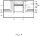
- An etch-back process is performed on the dielectric material 123 , in accordance with some embodiments to form an interlayer dielectric (ILD) layer 124 , as shown in FIG. 3 , in accordance with some embodiments.
- the etch-back process removes the dielectric material 123 , the oxide layer 121 , the nitride layer 119 , and the oxide layer 117 above the upper surface of the capping layer 114 until the upper surface of the capping layer 114 is exposed, in accordance with some embodiments.
- the etch-back process removes an upper portion of the first nitride spacer 116 .
- the oxide layer 117 , the nitride layer 119 , and the oxide layer 121 forms a first oxide spacer 118 , a second nitride spacer 120 , and a second oxide spacer 122 , respectively, in accordance with some embodiments.
- the upper surfaces of the ILD layer 124 , the second oxide spacer 122 , the second nitride spacer 120 , the first oxide spacer 118 , the first nitride spacer 116 , and the capping layer 114 are substantially coplanar, in accordance with some embodiments.
- the first oxide spacer 118 , the second nitride spacer 120 , and the second oxide spacer 122 each have a vertical portion extending along the sidewall of the gate stack 104 and a horizontal portion extending along the upper surface of the semiconductor substrate 102 , in accordance with some embodiments.
- the second oxide spacer 122 which contacts the ILD layer 124 , may provide oxygen atoms for ILD layer 124 to enhance the ability of the ILD layer 124 against dielectric breakdown, in accordance with some embodiments.
- a cleaning process 126 is performed on the semiconductor substrate 102 , as shown in FIG. 4 , in accordance with some embodiments.
- the cleaning process 126 is a post cleaning process after an etching process to clean another region (not shown) of the semiconductor substrate 102 .
- the etching process is used to form a gate structure in another region (not shown) of the semiconductor substrate 102 .
- the cleaning process 126 removes particles, byproducts, and/or oxides, which are produced in the etching process, from the semiconductor substrate 102 , in accordance with some embodiments.
- the cleaning process 126 uses a fluorine-containing solution such as a dilute hydrofluoric (DHF) acid and/or a buffer agent, in accordance with some embodiments.
- DHF dilute hydrofluoric
- the cleaning process 126 removes an upper portion of the vertical portion of the second oxide spacer 122 , thereby forming a void 128 , as shown in FIG. 4 , in accordance with some embodiments.
- the void 128 exposes the sidewall of the ILD layer 124 and the sidewall of the second nitride spacer 120 , in accordance with some embodiments.
- the anneal process performed on the dielectric material 123 may result in a decrease in the adhesion between the ILD layer 124 and the second oxide spacer 122 and/or forms a gap between the ILD layer 124 and the second oxide spacer 122 .
- the fluorine-containing solution of the cleaning process 126 may cause the upper portion of the vertical portion of the second oxide spacer 122 to be peeled off, thereby forming the void 128 .
- the second oxide spacer 122 on one side of the gate stack 104 is peeled off to form the void 128 while the second oxide spacer 122 on one another side of the gate stack 104 is not peeled off, as shown in FIG. 4 .
- the void 128 has a bottom portion having a convex profile. In other words, the upper surface of the second oxide spacer 122 exposed from the void 128 has a concave profile. In some embodiments, the void 128 has a depth D that ranges from about 1 nm to about 20 nm.
- An oxide layer 130 is conformally formed along the sidewalls and the bottom surface of the void 128 (i.e., the sidewall of the ILD layer 124 , the sidewall of the second nitride spacer 120 , and the upper surface of the second oxide spacer 122 exposed from the void 128 ), as shown in FIG. 5 , in accordance with some embodiments.
- the oxide layer 130 is further formed along the upper surfaces of the ILD layer 124 , the second nitride spacer 120 , the first oxide spacer 118 , the first nitride spacer 116 , and the capping layer 112 , in accordance with some embodiments.
- the oxide layer 130 has a thickness that is less than about 5 nm, such as in a range from about 0.5 nm to about 5 nm, such as about 2 nm.
- the oxide layer 130 is silicon oxide.
- the oxide layer 130 is formed by ISSG, ALD process, CVD, or a combination thereof.
- a nitride layer 132 is formed on the oxide layer 130 , as shown in FIG. 5 , in accordance with some embodiments.
- the nitride layer 132 is filled into the remaining portion of the void 128 and formed over the ILD layer 124 , the second nitride spacer 120 , the first oxide spacer 118 , the first nitride spacer 116 , and the capping layer 114 , in accordance with some embodiments.
- additional void may be formed in the nitride layer 132 during forming the nitride layer 132 .
- the nitride layer 132 is silicon nitride. In some embodiments, the nitride layer 132 is formed by CVD such as PECVD, ALD, or a combination thereof.
- the nitride layer 132 formed over the upper surface of the ILD layer 124 , is removed, as shown in FIG. 6 , in accordance with some embodiments.
- the oxide layer 130 formed along the upper surfaces of the ILD layer 124 , the second nitride spacer 120 , the first oxide spacer 118 , the first nitride spacer 116 , and the capping layer 114 , is exposed after the removal process, in accordance with some embodiments.
- a remaining portion 132 ′ of the nitride layer 132 remains in the void 128 , in accordance with some embodiments.
- the removal process includes CMP and followed by an etch-back process, in accordance with some embodiments.
- the etch-back process is a wet etching using a phosphoric acid.
- the oxide layer 130 is used as an etching stop layer to protect nitrogen-containing material underlying the oxide layer 130 (e.g., the capping layer 114 , the first nitride spacer 116 , and/or the second nitride spacer 120 ) from being removed during the etch-back process, in accordance with some embodiments.
- nitrogen-containing material underlying the oxide layer 130 e.g., the capping layer 114 , the first nitride spacer 116 , and/or the second nitride spacer 120 .
- the upper surface of the nitride layer 132 ′ is located at a level less than the upper surface of the ILD layer 124 to form a recess 134 , as shown in FIG. 6 , in accordance with some embodiments.
- the recess 132 has a less depth than the void 128 , such as less than about 2 nm.
- a tri-layer mask structure is formed over the semiconductor substrate 102 , as shown in FIG. 7 , in accordance with some embodiments.
- the tri-layer mask structure includes a bottom layer 136 , a middle layer 138 , and a top layer 140 which are sequentially formed over upper surfaces of the oxide layer 130 and the nitride layer 132 ′, in accordance with some embodiments.
- a lithography process is performed on the top layer 140 to form openings 142 exposing the upper surface of the middle layer 138 , in shown in FIG. 7 , in accordance with some embodiments.
- the bottom layer 136 is made of a nitrogen-free material such as carbon or silicon oxycarbide (SiOC).
- the middle layer is an antireflection coating (ARC) layer such as silicon oxynitride (SiON).
- ARC antireflection coating
- SiON silicon oxynitride
- the top layer 140 is made of a photoresist material.
- An etching process is performed on the ILD layer 124 , the second oxide spacer 122 , the second nitride spacer 120 , and the first oxide spacer 118 through the openings 142 of the top layer 140 to form openings 144 , as shown in FIG. 8 , in accordance with some embodiments.
- the openings 144 pass through the ILD layer 124 and the horizontal portions of the second oxide spacer 122 , the second nitride spacer 120 , and first oxide spacer 118 to expose the upper surface of the semiconductor substrate 102 , in accordance with some embodiments.
- the etching process is dry etching.
- the tri-layer mask structure above the upper surface of the ILD layer 124 is removed using such as ash process, wet strip process, or a combination thereof, in accordance with some embodiments.
- a cleaning process is performed on the semiconductor substrate 102 , in accordance with some embodiments.
- the cleaning process removes particles, byproducts, and/or oxides over the semiconductor substrate 102 , in accordance with some embodiments.
- the cleaning process uses a fluorine-containing solution such as a DHF acid and/or a buffer agent.
- the cleaning process removes the oxide layer 130 formed over the upper surfaces of the ILD layer 124 , the second nitride spacer 120 , the first oxide spacer 118 , the first nitride spacer 116 , and the capping layer 114 , in accordance with some embodiments. After the cleaning process, a remaining portion 130 ′ the oxide layer 130 remains in the void 128 , in accordance with some embodiments.
- the oxide layer 130 ′ and the nitride layer 132 ′ collectively form a protection portion 133 , as shown in FIG. 8 , in accordance with some embodiments.
- the protection portion 133 is foiled between the ILD layer 124 and the vertical portion of the second nitride spacer 120 , in accordance with some embodiments.
- the protection portion 133 is formed above the vertical portion of the second oxide spacer 122 , in accordance with some embodiments.
- the protection portion 133 has a bottom portion that has a convex profile.
- the convex profile of the protection portion 133 is mated with and contacts the upper surface of the second oxide spacer 122 having a concave profile.
- the sidewalls of protection portion 133 are aligned with the sidewalls of the vertical portion of the second oxide spacer 122 in accordance with some embodiments.
- a silicide 146 is formed in the bottom surface of the opening 144 (i.e., the upper surface of the semiconductor substrate 102 exposed from the opening 144 ), as shown in FIG. 9 , in accordance with some embodiments.
- the silicide 146 is cobalt silicide (CoSi), nickel silicide (NiSi), titanium silicide (TiSi), or a combination thereof.
- the steps of forming the silicide 146 may include a deposition process, an anneal process, and an etching process.
- a barrier layer 148 is conformally formed along the sidewalls of the opening PH (i.e., the surfaces of the ILD layer 124 , the second oxide spacer 122 , the second nitride spacer 120 , the first oxide spacer 118 exposed from opening 144 ) and the upper surface of the silicide 146 , as shown in FIG. 9 , in accordance with some embodiments.
- the barrier layer 148 is further conformally formed along the upper surfaces of the ILD layer 124 , the protection portion 133 , the second nitride spacer 120 , the first oxide spacer 118 , the first nitride spacer 116 , and the capping layer 114 , in accordance with some embodiments.
- the barrier layer 148 is formed in the recess 134 , in accordance with embodiments.
- the barrier layer 148 is made of titanium (Ti), tantalum (Ta), titanium nitride (TiN), tantalum nitride (TaN), or a combination thereof. In some embodiments, the barrier layer 148 is formed by ALD, PVD, or a combination thereof. In some embodiments, before the barrier layer 148 is formed, a pre-cleaning process may be performed on the semiconductor substrate 102 . In some embodiments, the pre-cleaning process uses the plasma of a reducing gas, such as argon (Ar) or NH 3 plasma, to remove native oxide.
- a reducing gas such as argon (Ar) or NH 3 plasma
- a metal material 150 is formed over the barrier layer 148 , as shown in FIG. 10 , in accordance with some embodiments.
- the metal material 150 is filled into the remaining portion of the opening 144 , in accordance with some embodiments.
- the metal material 150 is further formed in the recess 134 , in accordance with some embodiments.
- the metal material 150 is tungsten (W), copper (Cu), aluminum (Al), golden (Au), chromium (Cr), nickel (Ni), platinum (Pt), titanium (Ti), or a combination thereof. In some embodiments, the metal material 150 is formed by ALD, PVD, or a combination thereof.
- the removal process is CMP.
- the contacts 152 pass through the ILD layer 124 and the horizontal portions of the second oxide spacer 122 , the second nitride spacer 120 , and the first oxide spacer 118 land on the semiconductor substrate 102 , in accordance with some embodiments. In some embodiments, the contacts 152 land on and are in electrical connection with source/drain regions of the semiconductor substrate 102 .
- the upper surfaces of the ILD layer 124 , the protection portion 133 , the second nitride spacer 120 , the first oxide spacer 118 , the first nitride spacer 116 , and the capping layer 114 are exposed, in accordance with some embodiments.
- the recess 134 is removed in the removal process so that the upper surfaces of the second nitride spacer 120 , the first oxide spacer 118 , the first nitride spacer 116 , and the capping layer 114 are substantially coplanar, in accordance with some embodiments.
- a semiconductor structure 100 is produced.
- a capacitor structure (not shown) may be formed over the semiconductor structure 100 to form a DRAM.
- the semiconductor structure 100 includes the semiconductor substrate 102 and the gate stack 104 disposed over the semiconductor substrate 102 .
- the semiconductor structure 100 also includes the first nitride spacer 116 , the first oxide spacer 118 , the second nitride spacer 120 , and the second oxide spacer 122 sequentially disposed along a sidewall of the gate stack 104 .
- the semiconductor substrate 100 also includes the protection portion 133 disposed above the second oxide spacer 122 , and the ILD layer 124 disposed over the semiconductor substrate 102 .
- the protection portion 133 fills the void 128 (shown in FIG. 4 ) which is formed between the ILD layer 124 and the second nitride spacer 120 .
- the protection portion 133 formed over the second oxide spacer 122 and filled into the void 128 , prevents the conductive material (such as the silicide 146 , the barrier layer 148 , and/or the metal material 150 ) from being formed in the void 128 . Therefore, the protection portion avoids the electrical reliability issue caused by the formation of the conductive material in the void, thereby increasing the manufacturing yield and reliability of the semiconductor device.
Landscapes
- Engineering & Computer Science (AREA)
- Manufacturing & Machinery (AREA)
- Physics & Mathematics (AREA)
- Condensed Matter Physics & Semiconductors (AREA)
- General Physics & Mathematics (AREA)
- Computer Hardware Design (AREA)
- Microelectronics & Electronic Packaging (AREA)
- Power Engineering (AREA)
- Internal Circuitry In Semiconductor Integrated Circuit Devices (AREA)
- Semiconductor Memories (AREA)
Abstract
Description
Claims (16)
Priority Applications (1)
| Application Number | Priority Date | Filing Date | Title |
|---|---|---|---|
| US16/508,875 US11101179B2 (en) | 2019-07-11 | 2019-07-11 | Semiconductor structure with protection portions and method for forming the same |
Applications Claiming Priority (1)
| Application Number | Priority Date | Filing Date | Title |
|---|---|---|---|
| US16/508,875 US11101179B2 (en) | 2019-07-11 | 2019-07-11 | Semiconductor structure with protection portions and method for forming the same |
Publications (2)
| Publication Number | Publication Date |
|---|---|
| US20210013104A1 US20210013104A1 (en) | 2021-01-14 |
| US11101179B2 true US11101179B2 (en) | 2021-08-24 |
Family
ID=74102369
Family Applications (1)
| Application Number | Title | Priority Date | Filing Date |
|---|---|---|---|
| US16/508,875 Active 2039-09-08 US11101179B2 (en) | 2019-07-11 | 2019-07-11 | Semiconductor structure with protection portions and method for forming the same |
Country Status (1)
| Country | Link |
|---|---|
| US (1) | US11101179B2 (en) |
Cited By (1)
| Publication number | Priority date | Publication date | Assignee | Title |
|---|---|---|---|---|
| US11483001B2 (en) * | 2020-02-14 | 2022-10-25 | Kabushiki Kaisha Toshiba | Drive circuit and drive method of normally-on transistor |
Citations (6)
| Publication number | Priority date | Publication date | Assignee | Title |
|---|---|---|---|---|
| US20100022061A1 (en) * | 2008-07-24 | 2010-01-28 | Ming-Yuan Wu | Spacer Shape Engineering for Void-Free Gap-Filling Process |
| TW201318172A (en) | 2011-09-23 | 2013-05-01 | Semiconductor Energy Lab | Semiconductor device and method of manufacturing semiconductor device |
| TW201727769A (en) | 2011-11-30 | 2017-08-01 | 半導體能源研究所股份有限公司 | Semiconductor device manufacturing method |
| US20170263778A1 (en) * | 2016-03-09 | 2017-09-14 | Semiconductor Manufacturing International (Shanghai) Corporation | Flash memory structure and fabrication method thereof |
| TW201733128A (en) | 2011-12-27 | 2017-09-16 | 半導體能源研究所股份有限公司 | Semiconductor device and method of manufacturing semiconductor device |
| TW201905985A (en) | 2017-06-30 | 2019-02-01 | 台灣積體電路製造股份有限公司 | Method of fabricating a semiconductor device and method for reducing a dielectric constant of a gate spacer of a semiconductor device |
-
2019
- 2019-07-11 US US16/508,875 patent/US11101179B2/en active Active
Patent Citations (6)
| Publication number | Priority date | Publication date | Assignee | Title |
|---|---|---|---|---|
| US20100022061A1 (en) * | 2008-07-24 | 2010-01-28 | Ming-Yuan Wu | Spacer Shape Engineering for Void-Free Gap-Filling Process |
| TW201318172A (en) | 2011-09-23 | 2013-05-01 | Semiconductor Energy Lab | Semiconductor device and method of manufacturing semiconductor device |
| TW201727769A (en) | 2011-11-30 | 2017-08-01 | 半導體能源研究所股份有限公司 | Semiconductor device manufacturing method |
| TW201733128A (en) | 2011-12-27 | 2017-09-16 | 半導體能源研究所股份有限公司 | Semiconductor device and method of manufacturing semiconductor device |
| US20170263778A1 (en) * | 2016-03-09 | 2017-09-14 | Semiconductor Manufacturing International (Shanghai) Corporation | Flash memory structure and fabrication method thereof |
| TW201905985A (en) | 2017-06-30 | 2019-02-01 | 台灣積體電路製造股份有限公司 | Method of fabricating a semiconductor device and method for reducing a dielectric constant of a gate spacer of a semiconductor device |
Cited By (1)
| Publication number | Priority date | Publication date | Assignee | Title |
|---|---|---|---|---|
| US11483001B2 (en) * | 2020-02-14 | 2022-10-25 | Kabushiki Kaisha Toshiba | Drive circuit and drive method of normally-on transistor |
Also Published As
| Publication number | Publication date |
|---|---|
| US20210013104A1 (en) | 2021-01-14 |
Similar Documents
| Publication | Publication Date | Title |
|---|---|---|
| US11251070B2 (en) | Semiconductor device including a passivation spacer and method of fabricating the same | |
| KR101677345B1 (en) | Semiconductor structure and method making the same | |
| US8445991B2 (en) | Semiconductor device with MIM capacitor and method for manufacturing the same | |
| US20040038517A1 (en) | Methods of forming cobalt silicide contact structures including sidewall spacers for electrical isolation and contact structures formed thereby | |
| JP2001291867A (en) | Method of forming self-aligned contact pad in damascene gate process | |
| US10090155B2 (en) | Semiconductor device having interconnect structure | |
| US20220375828A1 (en) | Through-substrate via formation to enlarge electrochemical plating window | |
| CN108962879A (en) | Capacitor and method for manufacturing the same | |
| US11665889B2 (en) | Semiconductor memory structure | |
| US11101179B2 (en) | Semiconductor structure with protection portions and method for forming the same | |
| US20240153814A1 (en) | Methods of forming semiconductor device structures | |
| US9673200B2 (en) | Semiconductor device structure and method of manufacturing the same | |
| TWI872508B (en) | Semiconductor device and method of manufacturing the same | |
| US20070020844A1 (en) | Method for fabricating bit line of memory device | |
| TWI624090B (en) | Resistive random access memory device and method for manufacturing the same | |
| TWI685087B (en) | Semiconductor structures and methods for fabricating the same | |
| CN111952302B (en) | Semiconductor structure and manufacturing method thereof | |
| CN111326497A (en) | Conductive structure of semiconductor device | |
| TWI757193B (en) | Semiconductor memory structure and the method for forming the same | |
| TWI795178B (en) | Semiconductor device and method of forming the same | |
| CN221201172U (en) | Semiconductor structure | |
| CN115513206B (en) | Semiconductor memory structure and method for forming the same | |
| TWI861710B (en) | Dram and method for forming the same | |
| US11991875B2 (en) | Semiconductor memory structure and the method for forming the same | |
| CN115954324B (en) | Semiconductor structure and manufacturing method thereof |
Legal Events
| Date | Code | Title | Description |
|---|---|---|---|
| FEPP | Fee payment procedure |
Free format text: ENTITY STATUS SET TO UNDISCOUNTED (ORIGINAL EVENT CODE: BIG.); ENTITY STATUS OF PATENT OWNER: LARGE ENTITY |
|
| AS | Assignment |
Owner name: WINBOND ELECTRONICS CORP., TAIWAN Free format text: ASSIGNMENT OF ASSIGNORS INTEREST;ASSIGNORS:JEN, KAI;WANG, LI-TING;CHIEN, YI-HAO;REEL/FRAME:049777/0620 Effective date: 20190627 |
|
| STPP | Information on status: patent application and granting procedure in general |
Free format text: NON FINAL ACTION MAILED |
|
| STPP | Information on status: patent application and granting procedure in general |
Free format text: RESPONSE TO NON-FINAL OFFICE ACTION ENTERED AND FORWARDED TO EXAMINER |
|
| STPP | Information on status: patent application and granting procedure in general |
Free format text: NOTICE OF ALLOWANCE MAILED -- APPLICATION RECEIVED IN OFFICE OF PUBLICATIONS |
|
| STPP | Information on status: patent application and granting procedure in general |
Free format text: PUBLICATIONS -- ISSUE FEE PAYMENT RECEIVED |
|
| STPP | Information on status: patent application and granting procedure in general |
Free format text: PUBLICATIONS -- ISSUE FEE PAYMENT VERIFIED |
|
| STCF | Information on status: patent grant |
Free format text: PATENTED CASE |
|
| MAFP | Maintenance fee payment |
Free format text: PAYMENT OF MAINTENANCE FEE, 4TH YEAR, LARGE ENTITY (ORIGINAL EVENT CODE: M1551); ENTITY STATUS OF PATENT OWNER: LARGE ENTITY Year of fee payment: 4 |