US11094271B2 - Driving circuit of display panel and display device - Google Patents
Driving circuit of display panel and display device Download PDFInfo
- Publication number
- US11094271B2 US11094271B2 US17/043,565 US201817043565A US11094271B2 US 11094271 B2 US11094271 B2 US 11094271B2 US 201817043565 A US201817043565 A US 201817043565A US 11094271 B2 US11094271 B2 US 11094271B2
- Authority
- US
- United States
- Prior art keywords
- circuit
- electrically connected
- switching
- switching transistor
- output end
- Prior art date
- Legal status (The legal status is an assumption and is not a legal conclusion. Google has not performed a legal analysis and makes no representation as to the accuracy of the status listed.)
- Active
Links
- 238000004146 energy storage Methods 0.000 claims abstract description 39
- 239000003990 capacitor Substances 0.000 claims description 19
- 230000005669 field effect Effects 0.000 claims description 8
- 206010047571 Visual impairment Diseases 0.000 description 10
- 238000000034 method Methods 0.000 description 9
- 238000010586 diagram Methods 0.000 description 4
- 238000005516 engineering process Methods 0.000 description 4
- 230000006641 stabilisation Effects 0.000 description 3
- 238000011105 stabilization Methods 0.000 description 3
- 230000000694 effects Effects 0.000 description 2
- 239000010408 film Substances 0.000 description 2
- 239000004973 liquid crystal related substance Substances 0.000 description 2
- XUIMIQQOPSSXEZ-UHFFFAOYSA-N Silicon Chemical compound [Si] XUIMIQQOPSSXEZ-UHFFFAOYSA-N 0.000 description 1
- 230000006835 compression Effects 0.000 description 1
- 238000007906 compression Methods 0.000 description 1
- 229910044991 metal oxide Inorganic materials 0.000 description 1
- 150000004706 metal oxides Chemical class 0.000 description 1
- 238000012986 modification Methods 0.000 description 1
- 230000004048 modification Effects 0.000 description 1
- 230000000750 progressive effect Effects 0.000 description 1
- 229910052710 silicon Inorganic materials 0.000 description 1
- 239000010703 silicon Substances 0.000 description 1
- 239000000758 substrate Substances 0.000 description 1
- 239000010409 thin film Substances 0.000 description 1
Images


Classifications
-
- G—PHYSICS
- G09—EDUCATION; CRYPTOGRAPHY; DISPLAY; ADVERTISING; SEALS
- G09G—ARRANGEMENTS OR CIRCUITS FOR CONTROL OF INDICATING DEVICES USING STATIC MEANS TO PRESENT VARIABLE INFORMATION
- G09G3/00—Control arrangements or circuits, of interest only in connection with visual indicators other than cathode-ray tubes
- G09G3/20—Control arrangements or circuits, of interest only in connection with visual indicators other than cathode-ray tubes for presentation of an assembly of a number of characters, e.g. a page, by composing the assembly by combination of individual elements arranged in a matrix no fixed position being assigned to or needed to be assigned to the individual characters or partial characters
- G09G3/34—Control arrangements or circuits, of interest only in connection with visual indicators other than cathode-ray tubes for presentation of an assembly of a number of characters, e.g. a page, by composing the assembly by combination of individual elements arranged in a matrix no fixed position being assigned to or needed to be assigned to the individual characters or partial characters by control of light from an independent source
- G09G3/36—Control arrangements or circuits, of interest only in connection with visual indicators other than cathode-ray tubes for presentation of an assembly of a number of characters, e.g. a page, by composing the assembly by combination of individual elements arranged in a matrix no fixed position being assigned to or needed to be assigned to the individual characters or partial characters by control of light from an independent source using liquid crystals
-
- G—PHYSICS
- G09—EDUCATION; CRYPTOGRAPHY; DISPLAY; ADVERTISING; SEALS
- G09G—ARRANGEMENTS OR CIRCUITS FOR CONTROL OF INDICATING DEVICES USING STATIC MEANS TO PRESENT VARIABLE INFORMATION
- G09G3/00—Control arrangements or circuits, of interest only in connection with visual indicators other than cathode-ray tubes
- G09G3/20—Control arrangements or circuits, of interest only in connection with visual indicators other than cathode-ray tubes for presentation of an assembly of a number of characters, e.g. a page, by composing the assembly by combination of individual elements arranged in a matrix no fixed position being assigned to or needed to be assigned to the individual characters or partial characters
- G09G3/34—Control arrangements or circuits, of interest only in connection with visual indicators other than cathode-ray tubes for presentation of an assembly of a number of characters, e.g. a page, by composing the assembly by combination of individual elements arranged in a matrix no fixed position being assigned to or needed to be assigned to the individual characters or partial characters by control of light from an independent source
- G09G3/36—Control arrangements or circuits, of interest only in connection with visual indicators other than cathode-ray tubes for presentation of an assembly of a number of characters, e.g. a page, by composing the assembly by combination of individual elements arranged in a matrix no fixed position being assigned to or needed to be assigned to the individual characters or partial characters by control of light from an independent source using liquid crystals
- G09G3/3611—Control of matrices with row and column drivers
- G09G3/3648—Control of matrices with row and column drivers using an active matrix
-
- G—PHYSICS
- G09—EDUCATION; CRYPTOGRAPHY; DISPLAY; ADVERTISING; SEALS
- G09G—ARRANGEMENTS OR CIRCUITS FOR CONTROL OF INDICATING DEVICES USING STATIC MEANS TO PRESENT VARIABLE INFORMATION
- G09G3/00—Control arrangements or circuits, of interest only in connection with visual indicators other than cathode-ray tubes
- G09G3/20—Control arrangements or circuits, of interest only in connection with visual indicators other than cathode-ray tubes for presentation of an assembly of a number of characters, e.g. a page, by composing the assembly by combination of individual elements arranged in a matrix no fixed position being assigned to or needed to be assigned to the individual characters or partial characters
- G09G3/34—Control arrangements or circuits, of interest only in connection with visual indicators other than cathode-ray tubes for presentation of an assembly of a number of characters, e.g. a page, by composing the assembly by combination of individual elements arranged in a matrix no fixed position being assigned to or needed to be assigned to the individual characters or partial characters by control of light from an independent source
- G09G3/36—Control arrangements or circuits, of interest only in connection with visual indicators other than cathode-ray tubes for presentation of an assembly of a number of characters, e.g. a page, by composing the assembly by combination of individual elements arranged in a matrix no fixed position being assigned to or needed to be assigned to the individual characters or partial characters by control of light from an independent source using liquid crystals
- G09G3/3611—Control of matrices with row and column drivers
- G09G3/3696—Generation of voltages supplied to electrode drivers
-
- G—PHYSICS
- G09—EDUCATION; CRYPTOGRAPHY; DISPLAY; ADVERTISING; SEALS
- G09G—ARRANGEMENTS OR CIRCUITS FOR CONTROL OF INDICATING DEVICES USING STATIC MEANS TO PRESENT VARIABLE INFORMATION
- G09G2310/00—Command of the display device
- G09G2310/02—Addressing, scanning or driving the display screen or processing steps related thereto
- G09G2310/0243—Details of the generation of driving signals
- G09G2310/0245—Clearing or presetting the whole screen independently of waveforms, e.g. on power-on
-
- G—PHYSICS
- G09—EDUCATION; CRYPTOGRAPHY; DISPLAY; ADVERTISING; SEALS
- G09G—ARRANGEMENTS OR CIRCUITS FOR CONTROL OF INDICATING DEVICES USING STATIC MEANS TO PRESENT VARIABLE INFORMATION
- G09G2310/00—Command of the display device
- G09G2310/02—Addressing, scanning or driving the display screen or processing steps related thereto
- G09G2310/0264—Details of driving circuits
-
- G—PHYSICS
- G09—EDUCATION; CRYPTOGRAPHY; DISPLAY; ADVERTISING; SEALS
- G09G—ARRANGEMENTS OR CIRCUITS FOR CONTROL OF INDICATING DEVICES USING STATIC MEANS TO PRESENT VARIABLE INFORMATION
- G09G2310/00—Command of the display device
- G09G2310/06—Details of flat display driving waveforms
- G09G2310/061—Details of flat display driving waveforms for resetting or blanking
-
- G—PHYSICS
- G09—EDUCATION; CRYPTOGRAPHY; DISPLAY; ADVERTISING; SEALS
- G09G—ARRANGEMENTS OR CIRCUITS FOR CONTROL OF INDICATING DEVICES USING STATIC MEANS TO PRESENT VARIABLE INFORMATION
- G09G2320/00—Control of display operating conditions
- G09G2320/02—Improving the quality of display appearance
- G09G2320/0257—Reduction of after-image effects
-
- G—PHYSICS
- G09—EDUCATION; CRYPTOGRAPHY; DISPLAY; ADVERTISING; SEALS
- G09G—ARRANGEMENTS OR CIRCUITS FOR CONTROL OF INDICATING DEVICES USING STATIC MEANS TO PRESENT VARIABLE INFORMATION
- G09G2330/00—Aspects of power supply; Aspects of display protection and defect management
- G09G2330/02—Details of power systems and of start or stop of display operation
- G09G2330/021—Power management, e.g. power saving
-
- G—PHYSICS
- G09—EDUCATION; CRYPTOGRAPHY; DISPLAY; ADVERTISING; SEALS
- G09G—ARRANGEMENTS OR CIRCUITS FOR CONTROL OF INDICATING DEVICES USING STATIC MEANS TO PRESENT VARIABLE INFORMATION
- G09G2330/00—Aspects of power supply; Aspects of display protection and defect management
- G09G2330/02—Details of power systems and of start or stop of display operation
- G09G2330/027—Arrangements or methods related to powering off a display
Definitions
- This application relates to the technical field of liquid crystal display, and more specifically, relates to a drive circuit for a display panel, and a display device.
- TFT-LCD Thin film transistor liquid crystal display
- a main drive principle for a TFT-LCD is as follows: a system mainboard connects a red/green/blue (R/GB) compression signal (a tricolor signal), a control signal and power to a connector on a printed circuit board (PCB) through wires; data is processed by a timing controller (TC) integrated circuit (IC) on the PCB, passes through the PCB and is connected to a display region through a source-chip on film (S-COF) and a gate-chip on film (G-COF); and therefore, the LCD obtains required power and signals.
- R/GB red/green/blue
- TC timing controller
- IC integrated circuit
- a G-COF in a conventional architecture is integrated with an output all on (XAO) function. That is, in an off state, gate turning-on signals are output by all output of the G-COF to turn on all TFTs in a display panel and neutralize charges in pixel electrodes to avoid power-off afterimage caused by residual charges after power-off. Since a G-COF is integrated into an array substrate, it is impossible for a GOA technology to solve the problem of power-off afterimage.
- this application discloses a drive circuit for a display panel and a display device, to solve the problem of power-off afterimage in a GOA architecture, improve quality of a product and improve competitiveness of the product.
- a drive circuit for a display panel includes:
- a first circuit wherein a first preset voltage is input through a first input end of the first circuit, a second preset voltage is input through a second input end of the first circuit and the second input end of the first circuit is electrically connected to the energy storage circuit;
- a current limiting circuit wherein an input end of the current limiting circuit is electrically connected to an output end of a power supply;
- a first switching circuit wherein a first input end of the first switching circuit is electrically connected to an output end of the first circuit and an output end of the current limiting circuit respectively, a second input end of the first switching circuit is electrically connected to an output end of a drive chip, and an output end of the first switching circuit is electrically connected to the display panel;
- a second switching circuit wherein a first input end of the second switching circuit is electrically connected to the output end of the first circuit and the output end of the current limiting circuit respectively, a third preset voltage is input through a second input end of the second switching circuit, and an output end of the second switching circuit is electrically connected to the display panel, and wherein:
- the first circuit is configured to control the first switching circuit to be turned on or off, and the first circuit is further configured to control the second switching circuit to be turned on or off, so that when the first switching circuit is turned on, the second switching circuit is turned off, and when the second switching circuit is turned on, the first switching circuit is turned off.
- the energy storage circuit includes:
- a capacitor wherein one end of the capacitor is electrically connected to the second preset voltage and the second input end of the first circuit respectively and another end of the capacitor is grounded.
- the first circuit includes:
- a comparator wherein the first preset voltage is input through a first input end of the comparator, the second preset voltage is input through a second input end of the comparator, the second input end of the comparator is electrically connected to the energy storage circuit and an output end of the comparator is electrically connected to the first input end of the first switching circuit and the first input end of the second switching circuit respectively.
- the current limiting circuit includes:
- first resistor electrically connected to the first input end of the first switching circuit and the first input end of the second switching circuit respectively, and another end of the first resistor is electrically connected to the output end of the power supply.
- the first switching circuit includes:
- a first switching transistor wherein a gate of the first switching transistor is electrically connected to the output end of the first circuit and the output end of the current limiting circuit respectively, a source of the first switching transistor is electrically connected to the output end of the drive chip, and a drain of the first switching transistor is electrically connected to the display panel;
- the source of the first switching transistor is electrically connected to the display panel and the drain of the first switching transistor is electrically connected to the output end of the drive chip.
- the second switching circuit includes:
- a second switching transistor wherein a gate of the second switching transistor is electrically connected to the output end of the first circuit and the output end of the current limiting circuit respectively, the third preset voltage is input through a source of the second switching transistor, and a drain of the second switching transistor is electrically connected to the display panel;
- the source of the second switching transistor is electrically connected to the display panel and the third preset voltage is input through the drain of the second switching transistor.
- the drive circuit further includes:
- a step-down circuit electrically connected between the third preset voltage and the second input end of the second switching circuit.
- the step-down circuit includes:
- a second resistor wherein one end of the second resistor is electrically connected to the third preset voltage and another end of the second resistor is electrically connected to the second input end of the second switching circuit.
- a drive circuit for a display panel includes:
- a comparator wherein a first preset voltage is input through a first input end of the comparator, a second preset voltage is input through a second input end of the comparator and the second input end of the comparator is electrically connected to the energy storage circuit;
- a current limiting circuit wherein an input end of the current limiting circuit is electrically connected to an output end of a power supply;
- a first switching transistor wherein a first input end of the first switching transistor is electrically connected to an output end of the comparator and an output end of the current limiting circuit respectively, a second input end of the first switching transistor is electrically connected to an output end of a drive chip and an output end of the first switching transistor is electrically connected to the display panel;
- a second switching transistor wherein a first input end of the second switching transistor is electrically connected to the output end of the comparator and the output end of the current limiting circuit respectively, a third preset voltage is input through a second input end of the second switching transistor and an output end of the second switching transistor is electrically connected to the display panel, and wherein:
- the second switching transistor when the first switching transistor is turned on, the second switching transistor is turned off and, when the second switching transistor is turned on, the first switching transistor is turned off.
- the energy storage circuit, the first circuit, the current limiting circuit, the first switching circuit and the second switching circuit cooperate, and the first switching circuit and the second switching circuit are controlled through the first circuit to be turned on or off, so that the problem of power-off afterimage under a GOA architecture can be solved, quality of a product can be improved and competitiveness of the product can be further improved.
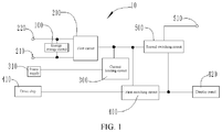
- FIG. 1 is a structure block diagram of a drive circuit according to an embodiment of this application.
- FIG. 2 is a circuit schematic diagram of a drive circuit according to an embodiment of this application.
- FIG. 3 is a structure block diagram of a drive circuit according to another embodiment of this application.
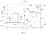
- FIG. 4 is a structure block diagram of a display according to an embodiment of this application.
- Embodiments of this application disclose a drive circuit for a display panel and a display device, to solve the problem of power-off afterimage in a GOA architecture, improve quality of a product and improve competitiveness of the product.
- an embodiment of this application provides a drive circuit, which includes an energy storage circuit 100 , a first circuit 200 , a current limiting circuit 300 , a first switching circuit 400 and a second switching circuit 500 .
- a first preset voltage 210 is input through a first input end of the first circuit 200 .
- a second preset voltage 220 is input through a second input end of the first circuit 200 and the second input end of the first circuit 200 is electrically connected to the energy storage circuit 100 .
- An input end of the current limiting circuit 300 is electrically connected to an output end of a power supply 310 .
- a first input end of the first switching circuit 400 is electrically connected to an output end of the first circuit 200 and an output end of the current limiting circuit 300 respectively.
- a second input end of the first switching circuit 400 is electrically connected to an output end of a drive chip 410 .
- An output end of the first switching circuit 400 is electrically connected to the display panel 420 .
- a first input end of the second switching circuit 500 is electrically connected to the output end of the first circuit 200 and the output end of the current limiting circuit 300 respectively.
- a third preset voltage 510 is input through a second input end of the second switching circuit 500 .
- An output end of the second switching circuit 500 is electrically connected to the display panel 420 .
- the first circuit 200 is configured to control the first switching circuit 400 to be turned on or off.
- the first circuit 200 is further configured to control the second switching circuit 500 to be turned on or off.
- the first switching circuit 400 is turned on, the second switching circuit 500 is turned off.
- the second switching circuit 500 is turned on, the first switching circuit 400 is turned off.
- the energy storage circuit 100 may be formed by a first capacitor. In an embodiment, the energy storage circuit 100 may formed by a storage battery. The specific configuration of the energy storage circuit 100 may be selected according to an actual requirement.
- the first preset voltage 210 is input through the first input end of the first circuit 200 .
- the first preset voltage 210 refers to an input voltage of the display panel 420 . It can be understood that a specific numerical value of the first preset voltage 210 is not limited as long as the first preset voltage 210 is constant.
- the first preset voltage 210 may be a direct current voltage of 12 V.
- the first preset voltage 210 may be a direct current voltage of 14 V.
- the specific numerical value of the first preset voltage 210 may be selected according to an actual requirement.
- the second preset voltage 220 is input through the second input end of the first circuit 200 .
- the second preset voltage 220 refers to a stabilized input voltage.
- a specific numerical value of the second preset voltage 220 is also not specifically limited.
- the second preset voltage 220 may be set to be 12 V or 14 V.
- the first circuit 200 may not be specifically limited as long as the first switching circuit 400 and the second switching circuit 500 may be controlled to be turned on and turned off based on the first preset voltage 210 and the second voltage 220 .
- the first circuit 200 may be formed by an operational amplifier. The operational amplifier outputs a control signal, thereby controlling the first switching circuit 400 and the second switching circuit 500 to be turned on and turned off.
- the first circuit 200 may also be formed by a first comparator. Specifically, when the first comparator outputs a high level, the first switching circuit 400 is turned off and the second switching circuit 500 is turned on. When the first comparator outputs a low level, the first switching circuit 400 is turned on and the second switching circuit 500 is turned off.
- the current limiting circuit 300 may not be specifically limited as long as safety of the drive circuit 10 is ensured.
- the current limiting circuit 300 may be formed by a resistor with fixed resistance.
- the current limiting circuit 300 may be formed by a sliding rheostat. The specific configuration may be selected according to an actual requirement.
- the first switching circuit 400 receives a control signal of the first circuit 200 .
- the control signal is a low level, the first switching circuit 400 is in an on state.
- the control signal is a high level, the first switching circuit 400 is in an off state.
- a specific configuration of the first switching circuit 400 may not be specifically limited as long as a function of switching according to the control signal output by the first circuit 200 may be ensured.
- the first switching circuit 400 is a relay control switch.
- the first switching circuit 400 is a switching transistor control switch.
- the second switching circuit 500 receives the control signal of the first circuit 200 .
- the control signal is a high level
- the second switching circuit 500 is in the off state.
- the control signal is a low level
- the second switching circuit 500 is in the on state.
- a specific configuration of the second switching circuit 500 may not be specifically limited as long as the function of switching according to the control signal output by the first circuit 200 may be ensured.
- the second switching circuit 500 is a relay control switch.
- the second switching circuit 500 is a switching transistor control switch.
- the energy storage circuit 100 , the first circuit 200 , the current limiting circuit 300 , the first switching circuit 400 and the second switching circuit 500 cooperate, and the first switching circuit 400 and the second switching circuit 500 are controlled through the first circuit 200 to be turned on and turned off, so that the problem of power-off afterimage under a GOA architecture can be solved, quality of a product can be improved and competitiveness of the product can be further improved.
- the energy storage circuit 100 includes a capacitor 110 .
- One end of the capacitor 110 is electrically connected to the second preset voltage 220 and the second input end of the first circuit 200 respectively, and another end of the capacitor 110 is grounded.
- the second preset voltage 220 is temporally kept at an original voltage and the first circuit 200 further outputs a high level.
- the first circuit 200 includes a comparator 230 .
- the first preset voltage 210 is input through a first input end of the comparator 230 .
- the second preset voltage 220 is input through a second input end of the comparator 230 and the second input end of the comparator 230 is electrically connected to the energy storage circuit 100 .
- An output end of the comparator 230 is electrically connected to the first input end of the first switching circuit 400 and the first input end of the second switching circuit 500 respectively.
- the comparator 230 when the comparator 230 outputs a high level, the first switching circuit 400 is turned off and the second switching circuit 500 is turned on. In an embodiment, when the comparator 230 outputs a low level, the first switching circuit 400 is turned on and the second switching circuit 500 is turned off. In an embodiment, the comparator 230 may also be replaced with an operational amplifier or the like.
- the current limiting circuit 300 includes a first resistor 320 .
- One end of the first resistor 320 is electrically connected to the first input end of the first switching circuit 400 and the first input end of the second switching circuit 500 respectively, and another end of the first resistor 320 is electrically connected to the output end of the power supply 310 .
- the first resistor 320 is a sliding rheostat with variable resistance.
- the first resistor 320 is a resistor with fixed resistance.
- the first switching circuit 400 includes a first switching transistor 430 .
- a gate of the first switching transistor 430 is electrically connected to the output end of the first circuit 200 and the output end of the current limiting circuit 300 .
- a source of the first switching transistor 430 is electrically connected to the output end of the drive chip 410 and a drain of the first switching transistor 430 is electrically connected to the display panel 420 .
- the source of the first switching transistor 430 is electrically connected to the display panel 420 and the drain of the first switching transistor 430 is electrically connected to the output end of the drive chip 410 .
- the drain of the first switching transistor 430 is electrically connected to the display panel 420 .
- the source of the first switching transistor 430 is electrically connected to the display panel 420 . That is, the drain and source of the first switching transistor 430 may be selected according to an actual requirement and a position relationship therebetween is not specifically limited.
- the first switching transistor 430 may adopt a first metal oxide silicon (MOS) transistor (field effect transistor) 431 .
- MOS metal oxide silicon
- the first switching transistor 430 may adopt an N-channel MOS transistor.
- the first switching transistor 430 may also adopt a P-channel MOS transistor. A specific configuration may be selected according to an actual requirement.
- the second switching circuit 500 includes a second switching transistor 520 .
- a gate of the second switching transistor 520 is electrically connected to the output end of the first circuit 200 and the output end of the current limiting circuit 300 respectively.
- the third preset voltage 510 is input through a source of the second switching transistor 410 and a drain of the second switching transistor 520 is electrically connected to the display panel 420 .
- the source of the second switching transistor 520 is electrically connected to the display panel 420 and the third preset voltage 510 is input through the drain of the second switching transistor 520 .
- the drain of the second switching transistor 520 is electrically connected to the display panel 420 .
- the source of the second switching transistor 520 is electrically connected to the display panel 420 . That is, the drain and source of the second switching transistor 520 may be selected according to an actual requirement and a position relationship therebetween is not specifically limited.
- the second switching transistor 520 may adopt a second MOS transistor (field effect transistor) 521 .
- the second switching transistor 520 may adopt an N-channel MOS transistor.
- the second switching transistor 520 may also adopt a P-channel MOS transistor.
- a specific configuration may be selected according to an actual requirement.
- the second switching transistor 520 adopts a P-channel MOS transistor and the first switching transistor 430 adopts an N-channel MOS transistor.
- the second switching transistor 520 adopts an N-channel MOS transistor and the first switching transistor 430 adopts a P-channel MOS transistor.
- a specific numerical value of the third preset voltage 510 is not limited as long as all TFTs in the display panel 420 are turned on. In an embodiment, the numerical value of the third preset voltage 510 may be 28 V. In an embodiment, the numerical value of the third preset voltage 510 may be 33 V. The specific numerical value of the third preset voltage 510 may be selected according to an actual requirement.
- the drive circuit 10 further includes a step-down circuit 530 , electrically connected between the third preset voltage 510 and the second input end of the second switching circuit 400 .
- a specific configuration of the step-down circuit 530 may not be specifically limited as long as the safety of the drive circuit 10 is ensured.
- the step-down circuit 530 may be formed by a resistor with fixed resistance.
- the step-down circuit 530 may be formed by a sliding rheostat with variable resistance. A specific configuration of the step-down circuit 530 may be selected according to an actual requirement.
- the step-down circuit 530 includes a second resistor 531 .
- One end of the second resistor 531 is electrically connected to the third preset voltage 510 .
- Another end of the second resistor 531 is electrically connected to the second input end of the second switching circuit 400 .
- a specific configuration of the second resistor 531 may not be specifically limited as long as the current limiting function may be realized.
- the second resistor 531 is a sliding rheostat with variable resistance.
- the second resistor 531 is a resistor with fixed resistance.
- an embodiment of this application provides a drive circuit for a display panel, which includes an energy storage circuit 100 , a comparator 230 , a current limiting circuit 300 , a first switching transistor 430 and a second switching transistor 520 .
- a first preset voltage 210 is input through a first input end of the comparator 230 .
- a second preset voltage 220 is input through a second input end of the comparator 230 and the second input end of the comparator 230 is electrically connected to the energy storage circuit 100 .
- An input end of the current limiting circuit 300 is electrically connected to an output end of a power supply 310 .
- a first input end of the first switching transistor 430 is electrically connected to an output end of the comparator 230 and an output end of the current limiting circuit 300 respectively.
- a second input end of the first switching transistor 430 is electrically connected to an output end of a drive chip 410 .
- An output end of the first switching transistor 430 is electrically connected to the display panel 420 .
- a first input end of the second switching transistor 520 is electrically connected to the output end of the comparator 230 and the output end of the current limiting circuit 300 respectively.
- a third preset voltage 510 is input through a second input end of the second switching transistor 520 .
- An output end of the second switching transistor 520 is electrically connected to the display panel 420 .
- the energy storage circuit 100 may be formed by a first capacitor. In an embodiment, the energy storage circuit 100 may be formed by a storage battery. The specific configuration of the energy storage circuit 100 may be selected according to an actual requirement.
- the first preset voltage 210 refers to an input voltage of the display panel 420 . It can be understood that a specific numerical value of the first preset voltage 210 is not limited as long as the first preset voltage 210 is constant. In an embodiment, the first preset voltage 210 may be a direct current voltage of 12 V. In an embodiment, the first preset voltage 210 may be a direct current voltage of 14 V. The specific numerical value of the first preset voltage 210 may be selected according to an actual requirement.
- the second preset voltage 220 refers to a stabilized input voltage. Similarly, a specific numerical value of the second preset voltage 220 is also not specifically limited. In an embodiment, the second preset voltage 220 may be set to be 12 V or 14 V.
- the comparator 230 when the comparator 230 outputs a high level, the first switching transistor 430 is turned off and the second switching transistor 520 is turned on. In an embodiment, when the comparator 230 outputs a low level, the first switching transistor 430 is turned on and the second switching transistor 520 is turned off. In an embodiment, the comparator 230 may also be replaced with an operational amplifier and the like.
- the current limiting circuit 300 may not be specifically limited as long as safety of the drive circuit 10 is ensured.
- the current limiting circuit 300 may be formed by a resistor with fixed resistance.
- the current limiting circuit 300 may be formed by a sliding rheostat. The specific configuration may be selected according to an actual requirement.
- the first switching transistor 430 receives a control signal of the comparator 230 .
- the control signal is a low level
- the first switching transistor 430 is in an on state.
- the control signal is a high level
- the first switching transistor 430 is in an off state.
- a specific configuration of the first switching transistor 430 may not be specifically limited as long as a function of switching according to the control signal output by the comparator 230 may be ensured.
- the first switching transistor 430 may be a relay control switch.
- the first switching transistor 430 may be an MOS transistor switch.
- the second switching transistor 520 receives the control signal of the comparator 230 .
- the control signal is a high level
- the second switching transistor 520 is in the off state.
- the control signal is a low level
- the second switching transistor 520 is in the on state.
- a specific configuration of the second switching transistor 520 may not be specifically limited as long as the function of switching according to the control signal output by the comparator 230 may be ensured.
- the second switching transistor 520 is a relay control switch.
- the second switching transistor 520 is a switching transistor control switch.
- the energy storage circuit 100 , the comparator 230 , the current limiting circuit 300 , the first switching transistor 430 and the second switching transistor 520 cooperate, and the first switching transistor 430 and the second switching transistor 520 are controlled through the comparator 230 to be turned on and turned off, so that the problem of power-off afterimage under a GOA architecture can be solved, quality of a product can be improved and competitiveness of the product can be further improved.
- the second switching circuit 500 adopts an N-channel MOS transistor.
- the N-channel MOS transistor When a control signal received by a gate of the N-channel MOS transistor is a high level, the N-channel MOS transistor is turned on. When the control signal received by the gate of the N-channel MOS transistor is a low level, the N-channel MOS transistor is turned off.
- the first switching circuit 400 adopts a P-channel MOS transistor. When a control signal received by a gate of the P-channel MOS transistor is a low level, the P-channel MOS transistor is turned on. When the control signal received by the gate of the P-channel MOS transistor is a high level, the P-channel MOS transistor is turned off.
- the first circuit 200 may adopt the comparator 230 .
- the capacitor 110 adopted for the energy storage circuit 100 is a voltage stabilization capacitor.
- the negative voltage of the comparator 230 is a constant direct current voltage (i.e., the first preset voltage 210 , which is generally 12 V).
- the positive voltage (i.e., the second preset voltage 220 ) of the comparator 230 is equal to the negative voltage (i.e., the first preset voltage 210 ), that is, the comparator 230 outputs a low level.
- the control signals received by the gates of the N-channel MOS transistor and the P-channel MOS transistor are both low levels. In this case, the P-channel MOS transistor is turned on and the N-channel MOS transistor is turned off. In this case, an output voltage of the drive chip 410 is equal to an input voltage of the display panel 420 .
- an external input voltage i.e., the first preset voltage 210
- the second preset voltage 220 is temporally kept at the original voltage (that is, the positive voltage of the comparator 230 is higher than the negative voltage).
- the comparator 230 outputs a high level. That is, the control signals received by the gates of the N-channel MOS transistor and the P-channel MOS transistor are both high levels.
- the P-channel MOS transistor is turned off and the N-channel MOS transistor is turned on.
- the input voltage of the display panel 420 is equal to the third preset voltage 510 . That is, all the TFTs in the display panel 420 are turned on to neutralize charges in pixel electrodes to avoid power-off afterimage caused by residual charges after power-off.
- the energy storage circuit 100 , the first circuit 200 , the current limiting circuit 300 , the first switching circuit 400 and the second switching circuit 500 cooperate, and the first switching circuit 400 and the second switching circuit 500 are controlled through the first circuit 200 to be turned on and turned off, so that the problem of power-off afterimage under a GOA architecture can be solved, quality of a product can be improved and competitiveness of the product can be further improved.
- an embodiment of this application also provides a display device 20 , which includes a display panel 420 and the drive circuit 10 according to any foregoing embodiment.
Landscapes
- Engineering & Computer Science (AREA)
- Chemical & Material Sciences (AREA)
- Crystallography & Structural Chemistry (AREA)
- Physics & Mathematics (AREA)
- Computer Hardware Design (AREA)
- General Physics & Mathematics (AREA)
- Theoretical Computer Science (AREA)
- Control Of Indicators Other Than Cathode Ray Tubes (AREA)
Applications Claiming Priority (3)
| Application Number | Priority Date | Filing Date | Title |
|---|---|---|---|
| CN201811338866.8A CN109147710A (zh) | 2018-11-12 | 2018-11-12 | 显示面板的驱动电路及显示装置 |
| CN201811338866.8 | 2018-11-12 | ||
| PCT/CN2018/117730 WO2020097978A1 (zh) | 2018-11-12 | 2018-11-27 | 显示面板的驱动电路及显示装置 |
Publications (2)
| Publication Number | Publication Date |
|---|---|
| US20210035510A1 US20210035510A1 (en) | 2021-02-04 |
| US11094271B2 true US11094271B2 (en) | 2021-08-17 |
Family
ID=64808233
Family Applications (1)
| Application Number | Title | Priority Date | Filing Date |
|---|---|---|---|
| US17/043,565 Active US11094271B2 (en) | 2018-11-12 | 2018-11-27 | Driving circuit of display panel and display device |
Country Status (3)
| Country | Link |
|---|---|
| US (1) | US11094271B2 (zh) |
| CN (1) | CN109147710A (zh) |
| WO (1) | WO2020097978A1 (zh) |
Families Citing this family (5)
| Publication number | Priority date | Publication date | Assignee | Title |
|---|---|---|---|---|
| CN109243398A (zh) * | 2018-11-12 | 2019-01-18 | 惠科股份有限公司 | 显示面板的驱动电路及显示装置 |
| CN109147710A (zh) * | 2018-11-12 | 2019-01-04 | 惠科股份有限公司 | 显示面板的驱动电路及显示装置 |
| CN109903731A (zh) * | 2019-03-20 | 2019-06-18 | 惠科股份有限公司 | 显示面板的驱动电路及显示面板 |
| CN113643644B (zh) * | 2021-10-14 | 2022-01-14 | 惠科股份有限公司 | 电流控制电路、显示面板驱动装置及显示装置 |
| CN115148141B (zh) * | 2022-06-27 | 2023-03-03 | 绵阳惠科光电科技有限公司 | 栅极驱动电路、栅极驱动方法和显示装置 |
Citations (26)
| Publication number | Priority date | Publication date | Assignee | Title |
|---|---|---|---|---|
| US6271812B1 (en) * | 1997-09-25 | 2001-08-07 | Denso Corporation | Electroluminescent display device |
| US20020196223A1 (en) * | 1998-04-16 | 2002-12-26 | Kotoyoshi Takahashi | Method for controlling liquid crystal display device, device for driving liquid crystal display device, liquid crystal display device, and electronic apparatus |
| US20050099376A1 (en) * | 2003-10-09 | 2005-05-12 | Toppoly Optoelectronics Corp. | Image sticking elimination circuit |
| KR20050097038A (ko) | 2004-03-30 | 2005-10-07 | 엘지.필립스 엘시디 주식회사 | 아날로그 버퍼 및 그의 구동 방법 |
| US20070176866A1 (en) * | 2006-01-31 | 2007-08-02 | Toppoly Optoelectronics Corp. | Display panel with image sticking elimination circuit and driving circuit with the same |
| US20070182670A1 (en) * | 2003-06-16 | 2007-08-09 | Hitachi, Ltd. | Display device having a circuit protection function |
| JP3979498B2 (ja) | 2003-10-07 | 2007-09-19 | ▲ぎょく▼瀚科技股▲ふん▼有限公司 | 液晶表示器の駆動回路及び駆動方法 |
| CN101183504A (zh) | 2006-11-14 | 2008-05-21 | 中华映管股份有限公司 | 驱动装置 |
| US20090097180A1 (en) * | 2007-10-10 | 2009-04-16 | Innocom Technology (Shenzhen) Co., Ltd. | Backlight control circuit with protecting circuit |
| US20100097365A1 (en) * | 2008-10-17 | 2010-04-22 | Wen-Chen Fang | Liquid crystal display device and control method thereof |
| US20110075063A1 (en) * | 2009-09-28 | 2011-03-31 | Sony Corporation | Liquid crystal display device |
| US20130241416A1 (en) * | 2010-09-29 | 2013-09-19 | European Intelligence B.V. | Intrinsically Safe Display Device with an Array of LEDS |
| US20130249876A1 (en) | 2012-03-26 | 2013-09-26 | Innolux Corporation | Shift register apparatus and display system utilizing the same |
| CN103761953A (zh) | 2014-01-28 | 2014-04-30 | 北京京东方显示技术有限公司 | 一种显示控制单元及显示装置 |
| US20140176855A1 (en) * | 2012-12-20 | 2014-06-26 | Shenzhen China Star Optoelectronics Technology Co. Ltd. | Led backlight driving circuit and lcd device |
| US20150309550A1 (en) * | 2014-04-24 | 2015-10-29 | Synaptics Display Devices Gk | Mobile terminal and display panel driver |
| CN106952628A (zh) | 2017-05-05 | 2017-07-14 | 惠科股份有限公司 | 一种残影消除电路及显示装置 |
| US20170206851A1 (en) * | 2016-01-15 | 2017-07-20 | Boe Technology Group Co., Ltd. | Control device and control method for display module, and display device |
| US20170345372A1 (en) * | 2015-10-08 | 2017-11-30 | Boe Technology Group Co., Ltd. | Gate driving apparatus for pixel array and driving method therefor |
| US20180240414A1 (en) * | 2016-06-17 | 2018-08-23 | Boe Technology Group Co., Ltd. | Circuit for removing residual image after power-off, method for driving same, and display apparatus |
| US20190130865A1 (en) * | 2017-10-31 | 2019-05-02 | Boe Technology Group Co., Ltd. | Control circuit, control method and display apparatus |
| US20190221183A1 (en) * | 2017-08-17 | 2019-07-18 | Chongqing Boe Optoelectronics Technology Co., Ltd. | Driving circuit for display device, voltage conversion circuit, display device and control method thereof |
| US20190235326A1 (en) * | 2018-01-29 | 2019-08-01 | Boe Technology Group Co., Ltd. | Discharge Circuit, Discharge Method and Display Device |
| US20200135131A1 (en) * | 2018-10-31 | 2020-04-30 | HKC Corporation Limited | Pre-charge method for display panel, display panel, and display device |
| US20210027690A1 (en) * | 2018-11-12 | 2021-01-28 | HKC Corporation Limited | Control circuit, display apparatus, and control method for control circuit |
| US20210035510A1 (en) * | 2018-11-12 | 2021-02-04 | HKC Corporation Limited | Driving circuit of display panel and display device |
-
2018
- 2018-11-12 CN CN201811338866.8A patent/CN109147710A/zh active Pending
- 2018-11-27 US US17/043,565 patent/US11094271B2/en active Active
- 2018-11-27 WO PCT/CN2018/117730 patent/WO2020097978A1/zh not_active Ceased
Patent Citations (41)
| Publication number | Priority date | Publication date | Assignee | Title |
|---|---|---|---|---|
| US6271812B1 (en) * | 1997-09-25 | 2001-08-07 | Denso Corporation | Electroluminescent display device |
| US20020196223A1 (en) * | 1998-04-16 | 2002-12-26 | Kotoyoshi Takahashi | Method for controlling liquid crystal display device, device for driving liquid crystal display device, liquid crystal display device, and electronic apparatus |
| US20070182670A1 (en) * | 2003-06-16 | 2007-08-09 | Hitachi, Ltd. | Display device having a circuit protection function |
| JP3979498B2 (ja) | 2003-10-07 | 2007-09-19 | ▲ぎょく▼瀚科技股▲ふん▼有限公司 | 液晶表示器の駆動回路及び駆動方法 |
| US7602364B2 (en) * | 2003-10-09 | 2009-10-13 | Tpo Displays Corp. | Image sticking elimination circuit |
| US20050099376A1 (en) * | 2003-10-09 | 2005-05-12 | Toppoly Optoelectronics Corp. | Image sticking elimination circuit |
| KR20050097038A (ko) | 2004-03-30 | 2005-10-07 | 엘지.필립스 엘시디 주식회사 | 아날로그 버퍼 및 그의 구동 방법 |
| US8040309B2 (en) * | 2006-01-31 | 2011-10-18 | Chimei Innolux Corproation | Display panel with image sticking elimination circuit and driving circuit with the same |
| US20070176866A1 (en) * | 2006-01-31 | 2007-08-02 | Toppoly Optoelectronics Corp. | Display panel with image sticking elimination circuit and driving circuit with the same |
| CN101183504A (zh) | 2006-11-14 | 2008-05-21 | 中华映管股份有限公司 | 驱动装置 |
| US20090097180A1 (en) * | 2007-10-10 | 2009-04-16 | Innocom Technology (Shenzhen) Co., Ltd. | Backlight control circuit with protecting circuit |
| US20100097365A1 (en) * | 2008-10-17 | 2010-04-22 | Wen-Chen Fang | Liquid crystal display device and control method thereof |
| US8711137B2 (en) * | 2008-10-17 | 2014-04-29 | Hannstar Display Corporation | Liquid crystal display device with a control mechanism for eliminating images |
| US20110075063A1 (en) * | 2009-09-28 | 2011-03-31 | Sony Corporation | Liquid crystal display device |
| US8625039B2 (en) * | 2009-09-28 | 2014-01-07 | Japan Display West Inc. | Liquid crystal display device |
| US20140092074A1 (en) * | 2009-09-28 | 2014-04-03 | Japan Display West Inc. | Liquid crystal display device |
| US9159267B2 (en) * | 2009-09-28 | 2015-10-13 | Japan Display Inc. | Liquid crystal display device |
| US20130241416A1 (en) * | 2010-09-29 | 2013-09-19 | European Intelligence B.V. | Intrinsically Safe Display Device with an Array of LEDS |
| US20130249876A1 (en) | 2012-03-26 | 2013-09-26 | Innolux Corporation | Shift register apparatus and display system utilizing the same |
| US8803440B2 (en) * | 2012-12-20 | 2014-08-12 | Shenzhen China Star Optoelectronics Technology Co., Ltd | LED backlight driving circuit and LCD device |
| US20140176855A1 (en) * | 2012-12-20 | 2014-06-26 | Shenzhen China Star Optoelectronics Technology Co. Ltd. | Led backlight driving circuit and lcd device |
| CN103761953A (zh) | 2014-01-28 | 2014-04-30 | 北京京东方显示技术有限公司 | 一种显示控制单元及显示装置 |
| US20150309550A1 (en) * | 2014-04-24 | 2015-10-29 | Synaptics Display Devices Gk | Mobile terminal and display panel driver |
| US9541981B2 (en) * | 2014-04-24 | 2017-01-10 | Synaptics Japan Gk | Mobile terminal and display panel driver |
| US20170345372A1 (en) * | 2015-10-08 | 2017-11-30 | Boe Technology Group Co., Ltd. | Gate driving apparatus for pixel array and driving method therefor |
| US10629129B2 (en) * | 2015-10-08 | 2020-04-21 | Boe Technology Group Co., Ltd. | Gate driving apparatus for pixel array and driving method therefor |
| US10714045B2 (en) * | 2016-01-15 | 2020-07-14 | Boe Technology Group Co., Ltd. | Control device and control method for display module, and display device |
| US20170206851A1 (en) * | 2016-01-15 | 2017-07-20 | Boe Technology Group Co., Ltd. | Control device and control method for display module, and display device |
| US20180240414A1 (en) * | 2016-06-17 | 2018-08-23 | Boe Technology Group Co., Ltd. | Circuit for removing residual image after power-off, method for driving same, and display apparatus |
| US10438546B2 (en) * | 2016-06-17 | 2019-10-08 | Boe Technology Group Co., Ltd. | Circuit for removing residual image after power-off, method for driving same, and display apparatus |
| CN106952628A (zh) | 2017-05-05 | 2017-07-14 | 惠科股份有限公司 | 一种残影消除电路及显示装置 |
| US20200372871A1 (en) * | 2017-05-05 | 2020-11-26 | HKC Corporation Limited | Blur eliminating circuit |
| US20190221183A1 (en) * | 2017-08-17 | 2019-07-18 | Chongqing Boe Optoelectronics Technology Co., Ltd. | Driving circuit for display device, voltage conversion circuit, display device and control method thereof |
| US20190130865A1 (en) * | 2017-10-31 | 2019-05-02 | Boe Technology Group Co., Ltd. | Control circuit, control method and display apparatus |
| US10510316B2 (en) * | 2017-10-31 | 2019-12-17 | Boe Technology Group Co., Ltd. | Control circuit, control method and display apparatus |
| US20190235326A1 (en) * | 2018-01-29 | 2019-08-01 | Boe Technology Group Co., Ltd. | Discharge Circuit, Discharge Method and Display Device |
| US10747075B2 (en) * | 2018-01-29 | 2020-08-18 | Boe Technology Group Co., Ltd. | Discharge circuit, discharge method and display device |
| US20200135131A1 (en) * | 2018-10-31 | 2020-04-30 | HKC Corporation Limited | Pre-charge method for display panel, display panel, and display device |
| US10885864B2 (en) * | 2018-10-31 | 2021-01-05 | HKC Corporation Limited | Pre-charge method for display panel, display panel, and display device |
| US20210027690A1 (en) * | 2018-11-12 | 2021-01-28 | HKC Corporation Limited | Control circuit, display apparatus, and control method for control circuit |
| US20210035510A1 (en) * | 2018-11-12 | 2021-02-04 | HKC Corporation Limited | Driving circuit of display panel and display device |
Non-Patent Citations (2)
| Title |
|---|
| International Search Report dated Aug. 14, 2019, issued in corresponding International Application No. PCT/CN2018/117730, filed Nov. 27, 2018, 2 pages. |
| Notice of Reason for Rejection dated Dec. 3, 2019, issued in Chinese Application No. 201811338866.8, filed Nov. 12, 2018, 9 pages. |
Also Published As
| Publication number | Publication date |
|---|---|
| CN109147710A (zh) | 2019-01-04 |
| WO2020097978A1 (zh) | 2020-05-22 |
| US20210035510A1 (en) | 2021-02-04 |
Similar Documents
| Publication | Publication Date | Title |
|---|---|---|
| US11094271B2 (en) | Driving circuit of display panel and display device | |
| EP3627487B1 (en) | Overcurrent protection system and method for goa circuit | |
| US5793346A (en) | Liquid crystal display devices having active screen clearing circuits therein | |
| US7397471B2 (en) | Liquid crystal display device, power supply circuit, and method for controlling liquid crystal display device | |
| US10832628B2 (en) | Gate on-state voltage supply unit, gate on-state voltage supply method, display driving module and display device | |
| US11138946B2 (en) | Driving Method, driving circuit and display device | |
| CN207781164U (zh) | 一种残影消除电路、显示装置及其驱动电路 | |
| WO2018205321A1 (zh) | 显示装置及其省电方法 | |
| US7696646B2 (en) | Power switching circuit for liquid crystal display | |
| US10510297B2 (en) | Pixel circuit, driving method thereof, display panel and display device | |
| WO2019015184A1 (zh) | 开启电压调整电路及液晶显示装置 | |
| TW201301238A (zh) | 顯示裝置、液晶顯示裝置及驅動方法 | |
| US8223137B2 (en) | Liquid crystal display device and method for driving the same | |
| CN101556776B (zh) | 一种实现像素薄膜晶体管快速放电的驱动电路 | |
| US20080291192A1 (en) | Charge recycling system of liquid crystal display and charge recycling method thereof | |
| US20130249885A1 (en) | Display devices, sensing circuits and methods for sensing and compensating for threshold voltage shift of transistor | |
| WO2015000273A1 (zh) | 一种阵列基板、显示面板和显示装置 | |
| US20090267885A1 (en) | Pixel circuitry and driving method thereof | |
| US11488525B2 (en) | Display panel driving method of turning on an active switch corresponding to each pixel of the display panel for releasing charges stored in the display panel during operation, and drive circuit implementing the same | |
| CN104094344B (zh) | 液晶显示装置、液晶显示装置的驱动方法 | |
| US11158282B2 (en) | Driving circuit of display panel, and display device | |
| US7091965B2 (en) | Display device, method of driving the same, and electronic equipment | |
| JP2005037685A (ja) | 液晶表示パネルの駆動装置、及び液晶表示パネルの駆動方法 | |
| US11238822B2 (en) | Drive circuit and drive system | |
| CN119993081B (zh) | 耦合控制电路、显示驱动电路、阵列基板及显示面板 |
Legal Events
| Date | Code | Title | Description |
|---|---|---|---|
| AS | Assignment |
Owner name: HKC CORPORATION LIMITED, CHINA Free format text: ASSIGNMENT OF ASSIGNORS INTEREST;ASSIGNOR:HUANG, XIAOYU;REEL/FRAME:053929/0795 Effective date: 20200918 |
|
| FEPP | Fee payment procedure |
Free format text: ENTITY STATUS SET TO UNDISCOUNTED (ORIGINAL EVENT CODE: BIG.); ENTITY STATUS OF PATENT OWNER: LARGE ENTITY |
|
| STPP | Information on status: patent application and granting procedure in general |
Free format text: DOCKETED NEW CASE - READY FOR EXAMINATION |
|
| STPP | Information on status: patent application and granting procedure in general |
Free format text: NOTICE OF ALLOWANCE MAILED -- APPLICATION RECEIVED IN OFFICE OF PUBLICATIONS |
|
| STPP | Information on status: patent application and granting procedure in general |
Free format text: AWAITING TC RESP., ISSUE FEE NOT PAID |
|
| STPP | Information on status: patent application and granting procedure in general |
Free format text: NOTICE OF ALLOWANCE MAILED -- APPLICATION RECEIVED IN OFFICE OF PUBLICATIONS |
|
| STPP | Information on status: patent application and granting procedure in general |
Free format text: PUBLICATIONS -- ISSUE FEE PAYMENT RECEIVED |
|
| STPP | Information on status: patent application and granting procedure in general |
Free format text: PUBLICATIONS -- ISSUE FEE PAYMENT VERIFIED |
|
| STCF | Information on status: patent grant |
Free format text: PATENTED CASE |
|
| MAFP | Maintenance fee payment |
Free format text: PAYMENT OF MAINTENANCE FEE, 4TH YEAR, LARGE ENTITY (ORIGINAL EVENT CODE: M1551); ENTITY STATUS OF PATENT OWNER: LARGE ENTITY Year of fee payment: 4 |