US11088632B2 - Multi-channel inverter systems including coupled inductors - Google Patents
Multi-channel inverter systems including coupled inductors Download PDFInfo
- Publication number
- US11088632B2 US11088632B2 US16/557,324 US201916557324A US11088632B2 US 11088632 B2 US11088632 B2 US 11088632B2 US 201916557324 A US201916557324 A US 201916557324A US 11088632 B2 US11088632 B2 US 11088632B2
- Authority
- US
- United States
- Prior art keywords
- inverter
- winding
- leg
- coupled inductor
- inductor
- Prior art date
- Legal status (The legal status is an assumption and is not a legal conclusion. Google has not performed a legal analysis and makes no representation as to the accuracy of the status listed.)
- Active
Links
Images


Classifications
-
- H—ELECTRICITY
- H02—GENERATION; CONVERSION OR DISTRIBUTION OF ELECTRIC POWER
- H02M—APPARATUS FOR CONVERSION BETWEEN AC AND AC, BETWEEN AC AND DC, OR BETWEEN DC AND DC, AND FOR USE WITH MAINS OR SIMILAR POWER SUPPLY SYSTEMS; CONVERSION OF DC OR AC INPUT POWER INTO SURGE OUTPUT POWER; CONTROL OR REGULATION THEREOF
- H02M7/00—Conversion of AC power input into DC power output; Conversion of DC power input into AC power output
- H02M7/42—Conversion of DC power input into AC power output without possibility of reversal
- H02M7/44—Conversion of DC power input into AC power output without possibility of reversal by static converters
- H02M7/48—Conversion of DC power input into AC power output without possibility of reversal by static converters using discharge tubes with control electrode or semiconductor devices with control electrode
- H02M7/53—Conversion of DC power input into AC power output without possibility of reversal by static converters using discharge tubes with control electrode or semiconductor devices with control electrode using devices of a triode or transistor type requiring continuous application of a control signal
- H02M7/537—Conversion of DC power input into AC power output without possibility of reversal by static converters using discharge tubes with control electrode or semiconductor devices with control electrode using devices of a triode or transistor type requiring continuous application of a control signal using semiconductor devices only, e.g. single switched pulse inverters
-
- H—ELECTRICITY
- H02—GENERATION; CONVERSION OR DISTRIBUTION OF ELECTRIC POWER
- H02M—APPARATUS FOR CONVERSION BETWEEN AC AND AC, BETWEEN AC AND DC, OR BETWEEN DC AND DC, AND FOR USE WITH MAINS OR SIMILAR POWER SUPPLY SYSTEMS; CONVERSION OF DC OR AC INPUT POWER INTO SURGE OUTPUT POWER; CONTROL OR REGULATION THEREOF
- H02M1/00—Details of apparatus for conversion
- H02M1/0064—Magnetic structures combining different functions, e.g. storage, filtering or transformation
-
- H—ELECTRICITY
- H02—GENERATION; CONVERSION OR DISTRIBUTION OF ELECTRIC POWER
- H02M—APPARATUS FOR CONVERSION BETWEEN AC AND AC, BETWEEN AC AND DC, OR BETWEEN DC AND DC, AND FOR USE WITH MAINS OR SIMILAR POWER SUPPLY SYSTEMS; CONVERSION OF DC OR AC INPUT POWER INTO SURGE OUTPUT POWER; CONTROL OR REGULATION THEREOF
- H02M7/00—Conversion of AC power input into DC power output; Conversion of DC power input into AC power output
- H02M7/42—Conversion of DC power input into AC power output without possibility of reversal
- H02M7/44—Conversion of DC power input into AC power output without possibility of reversal by static converters
- H02M7/48—Conversion of DC power input into AC power output without possibility of reversal by static converters using discharge tubes with control electrode or semiconductor devices with control electrode
- H02M7/483—Converters with outputs that each can have more than two voltages levels
- H02M7/487—Neutral point clamped inverters
-
- H—ELECTRICITY
- H02—GENERATION; CONVERSION OR DISTRIBUTION OF ELECTRIC POWER
- H02M—APPARATUS FOR CONVERSION BETWEEN AC AND AC, BETWEEN AC AND DC, OR BETWEEN DC AND DC, AND FOR USE WITH MAINS OR SIMILAR POWER SUPPLY SYSTEMS; CONVERSION OF DC OR AC INPUT POWER INTO SURGE OUTPUT POWER; CONTROL OR REGULATION THEREOF
- H02M7/00—Conversion of AC power input into DC power output; Conversion of DC power input into AC power output
- H02M7/42—Conversion of DC power input into AC power output without possibility of reversal
- H02M7/44—Conversion of DC power input into AC power output without possibility of reversal by static converters
- H02M7/48—Conversion of DC power input into AC power output without possibility of reversal by static converters using discharge tubes with control electrode or semiconductor devices with control electrode
- H02M7/483—Converters with outputs that each can have more than two voltages levels
- H02M7/49—Combination of the output voltage waveforms of a plurality of converters
-
- H02M2007/4815—
-
- H—ELECTRICITY
- H02—GENERATION; CONVERSION OR DISTRIBUTION OF ELECTRIC POWER
- H02M—APPARATUS FOR CONVERSION BETWEEN AC AND AC, BETWEEN AC AND DC, OR BETWEEN DC AND DC, AND FOR USE WITH MAINS OR SIMILAR POWER SUPPLY SYSTEMS; CONVERSION OF DC OR AC INPUT POWER INTO SURGE OUTPUT POWER; CONTROL OR REGULATION THEREOF
- H02M7/00—Conversion of AC power input into DC power output; Conversion of DC power input into AC power output
- H02M7/42—Conversion of DC power input into AC power output without possibility of reversal
- H02M7/44—Conversion of DC power input into AC power output without possibility of reversal by static converters
- H02M7/48—Conversion of DC power input into AC power output without possibility of reversal by static converters using discharge tubes with control electrode or semiconductor devices with control electrode
- H02M7/4815—Resonant converters
-
- Y—GENERAL TAGGING OF NEW TECHNOLOGICAL DEVELOPMENTS; GENERAL TAGGING OF CROSS-SECTIONAL TECHNOLOGIES SPANNING OVER SEVERAL SECTIONS OF THE IPC; TECHNICAL SUBJECTS COVERED BY FORMER USPC CROSS-REFERENCE ART COLLECTIONS [XRACs] AND DIGESTS
- Y02—TECHNOLOGIES OR APPLICATIONS FOR MITIGATION OR ADAPTATION AGAINST CLIMATE CHANGE
- Y02B—CLIMATE CHANGE MITIGATION TECHNOLOGIES RELATED TO BUILDINGS, e.g. HOUSING, HOUSE APPLIANCES OR RELATED END-USER APPLICATIONS
- Y02B70/00—Technologies for an efficient end-user side electric power management and consumption
- Y02B70/10—Technologies improving the efficiency by using switched-mode power supplies [SMPS], i.e. efficient power electronics conversion e.g. power factor correction or reduction of losses in power supplies or efficient standby modes
Definitions
- the present invention relates to an apparatus, system and method for load balancing among multiple inverter units connected in parallel, and, in particular embodiments, to an apparatus, system and method for load balancing through a coupled inductor placed between parallel operated inverter units and an output filter.
- renewable energy sources include solar energy, wind power, tidal wave energy and the like.
- a solar power conversion system may include a plurality of solar panels connected in series or in parallel. The output of the solar panels may generate a variable dc voltage depending on a variety of factors such as time of day, location and sun tracking ability. In order to regulate the output of the solar panels, the output of the solar panels may be coupled to a dc/dc converter so as to achieve a regulated output voltage at the output of the dc/dc converter.
- the solar panels may be connected with a backup battery system through a battery charge control apparatus. During the day, the backup battery is charged through the output of the solar panels. When the power utility fails or the solar panels are an off-grid power system, the backup battery provides electricity to the loads coupled to the solar panels.
- a solar inverter is employed to convert the variable dc output of the photovoltaic modules to a 120 volts ac power source.
- a plurality of magnetic devices may be coupled between the solar inverter and the ac power source.
- a magnetic device typically includes a magnetic core formed of suitable magnetic materials such as ferrite, powder iron and/or the like.
- the magnetic device may further include a conductive winding or a plurality of conductive windings.
- the windings and the current flowing through the windings may generate a magnetic field, which is also known as magnetic flux.
- the magnetic core usually has a relatively high permeability in comparison with the surrounding medium (e.g., air).
- the magnetic flux is confined with the magnetic core, which forms a closed flux path.
- the magnetic flux provides a medium for storing, transferring or releasing electromagnetic energy.
- Coupled inductors are widely used in the power electronics industry.
- a coupled inductor may comprise two windings magnetically coupled to each other.
- the two coupled windings may be wound on a same magnetic core (e.g., a toroid core).
- the first winding generates a first magnetic force, which drives a first magnetic field or flux.
- the flux generated by the first winding is confined with the magnetic core, which forms a closed flux path.
- the second winding generates a second magnetic force, which drives a second magnetic field, which is confined with the magnetic core.
- the magnetic material of the magnetic core of a coupled inductor may be of a magnetic permeability greater than that of a surrounding medium (e.g., air).
- a surrounding medium e.g., air
- a system comprises a plurality of inverters having inputs connected to a dc power source, wherein the plurality of inverters is configured to operate with a phase shift from each other, and a coupled inductor comprising a plurality of windings, a first terminal of each winding of the plurality of windings is connected to one inverter of the plurality of inverter, wherein second terminals of the plurality of windings are connected together, and an output filter connected between the second terminals of the plurality of windings and an ac power source.
- a system comprises a first inverter, a second inverter and a third inverter connected between a dc power source and an ac power source, wherein the first inverter, the second inverter and the third inverter are connected in parallel through a coupled inductor having a first input, a second input and a third input connected to the first inverter, the second inverter and the third inverter respectively, and a phase shift is placed between output waveforms of two adjacent inverters.
- an inverter system comprises a first inverter connected between a dc power source and an input terminal of a first leg of a coupled inductor, a second inverter connected between the dc power source and an input terminal of a second leg of the coupled inductor, a third inverter connected between the dc power source and an input terminal of a third leg of the coupled inductor, and an output filter connected between the coupled inductor and an ac power source, wherein output terminals of the first leg, the second leg and the third leg of the coupled inductor are connected together and further connected to the output filter.
- An advantage of an embodiment of the present invention is a multi-channel inverter providing higher efficiency as well as lower total harmonic distortion (THD).
- FIG. 1 illustrates a block diagram of a multi-channel inverter system having a coupled inductor in accordance with various embodiments of the present disclosure
- FIG. 2 illustrates a schematic diagram of a first implementation of the multi-channel inverter system shown in FIG. 1 in accordance with various embodiments of the present disclosure
- FIG. 3 illustrates a schematic diagram of a second implementation of the multi-channel inverter system shown in FIG. 1 in accordance with various embodiments of the present disclosure
- FIG. 4 illustrates schematic diagrams of a third implementation of the multi-channel inverter system shown in FIG. 1 in accordance with various embodiments of the present disclosure
- FIG. 5 illustrates schematic diagrams of a fourth implementation of the multi-channel inverter system shown in FIG. 1 in accordance with various embodiments of the present disclosure
- FIG. 6 illustrates an implementation of the coupled inductor shown in FIG. 1 in accordance with various embodiments of the present disclosure
- FIG. 7 illustrates a schematic diagram of a three-phase system comprising the multi-channel inverter system shown in FIG. 1 in accordance with various embodiments of the present disclosure.
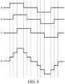
- FIG. 8 illustrates a multi-level waveform of the multi-channel inverter system shown in FIG. 2 in accordance with various embodiments of the present disclosure.
- the present invention will be described with respect to preferred embodiments in a specific context, namely a coupled inductor structure for connecting a plurality of inverter units of a phase of a dc/ac power system. Furthermore, the coupled inductor structure may be employed to connect three phases of the dc/ac power system. The invention may also be applied, however, to a variety of dc/ac power systems.
- various embodiments will be explained in detail with reference to the accompanying drawings.
- FIG. 1 illustrates a block diagram of a multi-channel inverter system having a coupled inductor in accordance with various embodiments of the present disclosure.
- the multi-channel inverter system 100 comprises an input dc power source 101 , a multi-channel inverter 102 , a coupled inductor 104 , an output filter 106 and an ac power source 107 .
- the multi-channel inverter 102 may comprises a plurality of power processing channels. Each channel may be implemented as a dc/ac inverter.
- the channels in the multi-channel inverter 102 are connected in parallel through the coupled inductor 104 .
- each channel is connected to the input dc power source 101 and the output of each channel is connected to an input of the output filter 106 through a winding of the coupled inductor 104 .
- Equal current sharing may be achieved through the coupled inductor 104 .
- the channels of the multi-channel inverter 102 may be alternatively referred to as the inverter units of the multi-channel inverter 102 .
- Each inverter unit of the multi-channel inverter 102 inverts a dc waveform received from the input dc power source 101 to an ac waveform.
- each inverter unit may comprise a plurality of switching elements such as insulated gate bipolar transistor (IGBT) devices.
- each inverter unit may include other types of controllable devices such as metal oxide semiconductor field effect transistor (MOSFET) devices, bipolar junction transistor (BJT) devices, super junction transistor (SJT) devices, bipolar transistors and/or the like.
- MOSFET metal oxide semiconductor field effect transistor
- BJT bipolar junction transistor
- SJT super junction transistor
- each channel is configured to invert a dc waveform into an ac waveform with a phase shift.
- the phase shift of each power processing channel is equal to 360 degrees divided by N, where N is the order of the most significant harmonic of the multi-channel inverter system 100 .
- N is an odd integer such as 5, 7 and the like.
- the coupled inductor 104 may comprise a plurality of windings magnetically coupled to each other.
- the plurality of windings may be negatively coupled to each other.
- the plurality of coupled windings may be wound on a same magnetic core (e.g., a toroid core).
- First terminals of the plurality of coupled windings are connected to their respective channels and second terminals of the plurality of coupled windings are connected together and further connected to the input of the output filter 106 .
- the coupling among the plurality of windings may generate leakage magnetic flux.
- the leakage magnetic flux is replaced by a leakage inductance.
- Such a leakage inductance may be employed to replace some inductive elements of the output filter 106 .
- the structure of the coupled inductor 104 will be described in detail below with respect to FIGS. 2-5 .
- the output filter 106 may comprise a plurality of inductive and capacitive elements.
- the inductive and capacitive elements may form an L-C filter or a plurality of L-C filters connected in cascade.
- the inductive elements e.g., inductors
- the capacitive elements e.g., capacitors
- the detailed structure of the output filter 106 will be described below with respect to FIGS. 2-5 .
- FIG. 2 illustrates a schematic diagram of a first implementation of the multi-channel inverter system shown in FIG. 1 in accordance with various embodiments of the present disclosure.
- An input dc voltage source PV 1 is coupled to the inputs of the multi-channel inverter 102 .
- input capacitors e.g., C 1 and C 2
- the input capacitors may comprise a first input capacitor C 1 and a second input capacitor C 2 .
- the first input capacitor C 1 and the second input capacitor C 2 are connected in series and further coupled between the two terminals of the input dc voltage source PV 1 .
- the common node of the first input capacitor C 1 and the second input capacitor C 2 is connected to a neural point as shown in FIG. 2 .
- the neural point is the ground of the multi-channel inverter system 200 .
- the multi-channel inverter 102 comprises a first inverter unit 202 , a second inverter unit 204 and a third inverter unit 206 .
- the inputs of the inverter units 202 , 204 and 206 are connected to the input dc voltage source PV 1 .
- the outputs of the inverter units 202 , 204 and 206 are connected to the three input terminals of the coupled inductor 104 respectively.
- the inverter units 202 , 204 and 206 shown in FIG. 2 are commonly known as T-type three-level inverters. It should be noted that while FIG. 2 shows the inverter units 202 , 204 and 206 are T-type three-level power inverters, it is within the scope and spirit of the invention for the multi-channel inverter system 200 to comprise other inverters, such as, but no limited to two-level inverters, three-level inverters, resonant inverters, any combinations thereof and/or the like.
- the inverter units 202 , 204 and 206 may be of a same structure such as the T-type three-level inverter structure shown in FIG. 2 .
- the inverter units 202 , 204 and 206 may be of a same structure such as the T-type three-level inverter structure shown in FIG. 2 .
- the first inverter unit 202 will be described below.
- the first inverter unit 202 comprises a pair of switching elements S 11 and S 12 connected in series.
- the common node of the switching elements S 11 and S 12 are coupled to ground through an isolation device formed by back-to-back connected switching elements S 13 and S 14 .
- the back-to-back connected switching elements S 13 and S 14 are capable of completely isolating the common node of the switching elements S 11 and S 12 from ground.
- switching elements S 11 , S 12 , S 13 and S 14 are IGBT or IGBTs connected in parallel, series and any combinations thereof.
- Switching elements S 11 , S 12 , S 13 and S 14 are so controlled that the output of the first inverter unit 202 generates a three level waveform.
- the output of the first inverter unit 202 when switching element S 11 is turned on and switching element S 12 is turned off, the output of the first inverter unit 202 generates a positive voltage equal to one half of the voltage of the input dc voltage source PV 1 .
- the output of the first inverter unit 202 generates a negative voltage equal to one half of the voltage of the input dc voltage source PV 1 .
- both switching elements S 11 and S 12 are turned off and switching elements S 13 and S 14 are turned on, the output of the first inverter unit 202 is coupled to ground. As such, the output of the first inverter unit 202 generates a three-level voltage waveform.
- the frequency of the three-level voltage waveform is approximately 60 HZ in accordance with an embodiment.
- each inverter unit shown in FIG. 2 are so controlled that there is a phase shift between two output waveforms.
- a first phase shift may be placed between the output of the first inverter unit 202 and the second inverter unit 204 .
- a second phase shift may be placed between the output of the second inverter unit 204 and the third inverter unit 206 .
- the voltage waveform at the output of the coupled inductor 104 is not a three-level waveform. Instead, the voltage waveform at the output of the coupled inductor 104 is a multi-level waveform.
- the number of levels of the multi-level waveform may vary depending on the degrees of the phase shifts. In some embodiments, the number of levels of the multi-level waveform is equal to seven. An example of a seven-level waveform is shown in FIG. 8 .
- multi-level waveform e.g., waveform D in FIG. 8
- the multilevel waveform shown in FIG. 8 follows the sinusoidal waveform.
- the harmonic contents are less.
- a dominant harmonic such as the fifth harmonic may be eliminated.
- the multilevel waveform helps to simplify the design of the output filter 106 . The detailed structure of the simplified output filter will be described below with respect to FIGS. 4-5 .
- the inverter units 202 , 204 and 206 and the coupled inductor 104 shown in FIG. 2 are merely examples, one person skilled in the art will realize that the inverters (e.g., inverter units 202 - 206 ) as well as its corresponding coupled inductor 104 may be implemented in many different ways.
- the multi-channel inverter system 200 may accommodate more than three inverter units.
- the coupled inductor 110 may comprise multiple windings, each of which is connected to one output of a corresponding inverter unit.
- the coupled inductor 104 comprises three windings.
- a first winding 212 is connected between node A and node D as shown in FIG. 2 .
- a second winding 214 is connected between node B and node D.
- a third winding 216 is connected between node C and node D.
- the dot of each winding denotes the polarity of the winding.
- the first winding 212 is negatively coupled to the second winding 214 with a coupling coefficient of M.
- the second winding 214 is negatively coupled to the third winding 216 with a coupling coefficient of M.
- the third winding 216 is negatively coupled to the first winding 212 with a coupling coefficient of M.
- M is a predetermined number. It may vary depending on different design needs. The detailed implementation of these three negatively coupled inductors will be described below with respect to FIG. 6 .
- the coupled inductor 104 helps the multi-channel inverter system 20 o distribute energy evenly between the first inverter unit 202 , the second inverter unit 204 and the third inverter unit 206 .
- the balance between these three inverter units is determined by the magnetizing inductances of the coupled inductor 104 .
- the magnetizing inductances are designed to have a large value. As a result, the variations of the magnetizing inductances are relatively small. Such small variations help the multi-channel inverter system 200 achieve both static current sharing and dynamic current sharing.
- the output filter 106 may comprise a first inductor L 1 and a second inductor L 2 connected in series and further coupled between the coupled inductor 104 and the output ac source.
- the output filter 106 may further comprise a plurality of output capacitors coupled between the common node of the first inductor L 1 and the second inductor L 2 , and ground.
- the plurality of output capacitors are collectively shown as a capacitor C 3 in FIG. 1 .
- the first inductor L 1 and the second inductor L 2 provide high impedance when high frequency noise tries to flow out of the multi-channel inverter system 200 .
- the capacitor C 3 shunts the input of the ac source and provides a low impedance channel for the high frequency noise generated from the multi-channel inverter system 200 .
- the high frequency noise of the inverter units 202 , 204 and 206 may be prevented from passing through the output filter 106 .
- the inverter topologies, the output filter 106 , the input dc power source PV 1 and the output ac power source shown in FIG. 2 are provided for illustrative purposes only, and are provided only as examples of various embodiments. Such examples should not unduly limit the scope of the claims.
- One of ordinary skill in the art would recognize many variations, alternatives, and modifications.
- FIG. 3 illustrates a schematic diagram of a second implementation of the multi-channel inverter system shown in FIG. 1 in accordance with various embodiments of the present disclosure.
- the multi-channel inverter system 300 shown in FIG. 3 is similar to that shown in FIG. 2 except that the first inductor L 1 has been replaced by the leakage inductance of the coupled inductor 104 . Since the voltage at the output of the coupled inductor 104 is a multilevel waveform following the sinusoidal waveform, the harmonic content is reduced accordingly. Such a low harmonic content helps to simplify the design of the output filter 106 . In some embodiments, the inductance of the first inductor L 1 may be reduced by 90%.
- the inductance of the first inductor L 1 is equal to about 10 uH. Such a small inductance can be replaced by the leakage inductance of the coupled inductor 104 . In other words, the first inductor L 1 can be integrated into the coupled inductor 104 .
- the magnetic material of the magnetic core may be of a magnetic permeability greater than that of a surrounding medium (e.g., air).
- a surrounding medium e.g., air
- the coupling between two inductors of the coupled inductor 104 may be not perfect.
- the coupling between the winding and the surrounding medium may generate leakage magnetic flux.
- All three inductors of the coupled inductor 104 may generate leakage inductance through the coupling with the surrounding medium such as air.
- the leakage generated by the first inductor winding is defined as L lk1 ;
- the leakage generated by the second inductor winding is defined as L lk2 ;
- the leakage generated by the third inductor winding is defined as L lk3 .
- FIG. 4 illustrates schematic diagrams of a third implementation of the multi-channel inverter system shown in FIG. 1 in accordance with various embodiments of the present disclosure.
- the multi-channel inverter system 400 shown in FIG. 4 is similar to that shown in FIG. 2 except that the output capacitor C 3 has been removed.
- One drawback of having an inductor-capacitor-inductor (LCL) filter shown in FIG. 2 is the LCL filter may lead to oscillation in the multi-channel inverter system 200 .
- LCL inductor-capacitor-inductor
- the capacitor C 3 may be removed and the multi-channel inverter system 400 may achieve the same harmonic elimination results (the current THD is equal to 1.8%) as the multi-channel inverter system 200 shown in FIG. 2 .
- One advantageous feature of removing the output capacitor C 3 is the behavior of the multi-channel inverter system 400 is similar to a current source generating a current following a sinusoidal waveform. Such a current source does not have the oscillation issue occurred in the inverter system having the LCL filter.
- FIG. 5 illustrates schematic diagrams of a fourth implementation of the multi-channel inverter system shown in FIG. 1 in accordance with various embodiments of the present disclosure.
- the multi-channel inverter system 500 shown in FIG. 5 is similar to that shown in FIG. 4 except that the first inductor L 1 has been replaced by the leakage inductance of the coupled inductor 104 .
- the mechanism of integrating the first inductor L 1 into the coupled inductor 104 has been described above in detail with respect to FIG. 3 , and hence is not discussed again to avoid unnecessary repetition.
- FIG. 6 illustrates an implementation of the coupled inductor shown in FIG. 1 in accordance with various embodiments of the present disclosure.
- the coupled inductor 104 may be wound around a magnetic core as shown in FIG. 6 .
- the magnetic core is made of a magnetic material having high permeability such as ferrite, powder iron, other power suitable materials, any combinations thereof and/or the like.
- the magnetic core may be made of suitable alloys such as silicon steel to further reduce the magnetic losses.
- FIG. 6 shows the coupled inductor 104 comprises three winding coils N 1 , N 2 and N 3 wound around a magnetic core having three legs.
- the first winding coil N 1 is wound around a first leg.
- the second winding coil N 2 is wound around a second leg.
- the third winding coil N 3 is wound around a third leg. As shown in FIG. 6 , the second leg is between the first leg and the third leg.
- the input terminals of the coils N 1 , N 2 and N 3 are connected to terminals A, B and C respectively.
- the output terminals of the coils N 1 , N 2 and N 3 are connected together and further connected to the terminal D.
- coils N 1 , N 2 and N 3 are wound in the same direction. In other words, the magnetic fields generated by windings N 1 , N 2 and N 3 are in the same direction.
- FIG. 7 illustrates a schematic diagram of a three-phase system comprising the multi-channel inverter system shown in FIG. 1 in accordance with various embodiments of the present disclosure.
- the three-phase system 700 includes phase A, phase B and phase C.
- the structures of phase B and phase C are similar to that of phase A, and hence are not shown in detail in FIG. 7 .
- phase A may be implemented as a multi-channel inverter 702 having three inverter units.
- the three inverter units of phase A are connected together through a first coupled inductor 712 .
- the operating principle of the multi-channel inverter 702 is similar to that of the multi-channel inverter system 200 shown in FIG. 2 , and hence is not discussed again to avoid unnecessary repetition.
- Phase A, phase B and phase C are connected together through a second coupled inductor 714 .
- the second coupled inductor 714 comprises windings 722 , 724 and 726 .
- the windings 722 , 724 and 726 are connected to loads AC 1 , AC 2 and AC 3 respectively through their corresponding output inductors L 11 , L 12 and L 3 .
- the structure of the second coupled inductor 714 is similar to that of the first coupled inductor 712 , and hence is not discussed again herein.
- FIG. 8 illustrates a multi-level waveform of the multi-channel inverter system shown in FIG. 2 in accordance with various embodiments of the present disclosure.
- FIG. 8 shows four waveforms.
- the first waveform is generated at the output of the first inverter unit 202 .
- the second waveform is generated at the output of the second inverter unit 204 .
- the third waveform is generated at the output of the third inverter unit 206 .
- the fourth waveform is generated at the output of the coupled inductor 104 .
- the fourth waveform has seven levels.
- the seven-level waveform follows a sinusoidal waveform. As a result, the harmonic contents are less.
Landscapes
- Engineering & Computer Science (AREA)
- Power Engineering (AREA)
- Inverter Devices (AREA)
Abstract
Description
Claims (20)
Priority Applications (1)
| Application Number | Priority Date | Filing Date | Title |
|---|---|---|---|
| US16/557,324 US11088632B2 (en) | 2015-11-05 | 2019-08-30 | Multi-channel inverter systems including coupled inductors |
Applications Claiming Priority (3)
| Application Number | Priority Date | Filing Date | Title |
|---|---|---|---|
| US14/933,723 US9923485B2 (en) | 2015-11-05 | 2015-11-05 | Multi-channel inverter systems |
| US15/924,853 US10404187B2 (en) | 2015-11-05 | 2018-03-19 | Multi-channel inverter systems including coupled inductors |
| US16/557,324 US11088632B2 (en) | 2015-11-05 | 2019-08-30 | Multi-channel inverter systems including coupled inductors |
Related Parent Applications (1)
| Application Number | Title | Priority Date | Filing Date |
|---|---|---|---|
| US15/924,853 Continuation US10404187B2 (en) | 2015-11-05 | 2018-03-19 | Multi-channel inverter systems including coupled inductors |
Publications (2)
| Publication Number | Publication Date |
|---|---|
| US20190386580A1 US20190386580A1 (en) | 2019-12-19 |
| US11088632B2 true US11088632B2 (en) | 2021-08-10 |
Family
ID=58662564
Family Applications (3)
| Application Number | Title | Priority Date | Filing Date |
|---|---|---|---|
| US14/933,723 Active US9923485B2 (en) | 2015-11-05 | 2015-11-05 | Multi-channel inverter systems |
| US15/924,853 Active US10404187B2 (en) | 2015-11-05 | 2018-03-19 | Multi-channel inverter systems including coupled inductors |
| US16/557,324 Active US11088632B2 (en) | 2015-11-05 | 2019-08-30 | Multi-channel inverter systems including coupled inductors |
Family Applications Before (2)
| Application Number | Title | Priority Date | Filing Date |
|---|---|---|---|
| US14/933,723 Active US9923485B2 (en) | 2015-11-05 | 2015-11-05 | Multi-channel inverter systems |
| US15/924,853 Active US10404187B2 (en) | 2015-11-05 | 2018-03-19 | Multi-channel inverter systems including coupled inductors |
Country Status (5)
| Country | Link |
|---|---|
| US (3) | US9923485B2 (en) |
| EP (1) | EP3360242A4 (en) |
| JP (2) | JP2018533354A (en) |
| CN (1) | CN108352789B (en) |
| WO (1) | WO2017076364A1 (en) |
Families Citing this family (21)
| Publication number | Priority date | Publication date | Assignee | Title |
|---|---|---|---|---|
| CN103944190B (en) * | 2014-04-30 | 2016-02-10 | 湖南大学 | A kind of stable state control method of three-phase dual mode inverter |
| US9923485B2 (en) | 2015-11-05 | 2018-03-20 | Futurewei Technologies, Inc. | Multi-channel inverter systems |
| PL3399630T3 (en) * | 2015-12-29 | 2022-06-13 | Ingeteam Power Technology, S.A. | Output filter for a power conversion system and power conversion system |
| TWI589736B (en) * | 2016-11-14 | 2017-07-01 | 國立清華大學 | Power converting device containing high frequency inverter and low frequency inverter connecting in parallel and the method thereof |
| US10763668B2 (en) * | 2017-11-01 | 2020-09-01 | Mediatek Inc. | Converter with inductors coupled in series |
| US11005388B2 (en) * | 2019-02-28 | 2021-05-11 | sonnen, Inc. | Single-phase multi-level asymmetric inverter with AC-bypass and asymmetric modulation strategy |
| CN111756226B (en) * | 2019-03-28 | 2024-05-31 | 维谛公司 | Inverter circuit, inverter, and control method and device of inverter circuit |
| WO2020101755A1 (en) | 2019-06-28 | 2020-05-22 | Huawei Technologies Co., Ltd. | Hybrid infeed with diode rectifier for bulk power and active bridge as rfc |
| CN115668737A (en) * | 2019-11-11 | 2023-01-31 | Abb电动汽车有限责任公司 | Multilevel power converter and method for a multilevel power converter |
| US11557983B2 (en) * | 2020-01-15 | 2023-01-17 | Solaredge Technologies Ltd. | Coupled inductors inverter topology |
| JP7413906B2 (en) * | 2020-04-17 | 2024-01-16 | 株式会社Gsユアサ | Inverter and rectifier circuit |
| TWI750649B (en) * | 2020-05-06 | 2021-12-21 | 國立清華大學 | Power converting device and method with high frequency inverter module compensating low frequency inverter module |
| US11794917B2 (en) | 2020-05-15 | 2023-10-24 | Pratt & Whitney Canada Corp. | Parallel control loops for hybrid electric aircraft |
| US11958622B2 (en) | 2020-05-15 | 2024-04-16 | Pratt & Whitney Canada Corp. | Protection functions |
| US11827372B2 (en) | 2020-05-15 | 2023-11-28 | Pratt & Whitney Canada Corp. | Engine characteristics matching |
| US12030651B2 (en) | 2021-01-05 | 2024-07-09 | Pratt & Whitney Canada Corp. | Parallel hybrid power plant with hollow motor |
| CN113162452B (en) * | 2021-03-29 | 2022-12-30 | 北京琦安电气技术有限公司 | Current phase-shifting parallel circuit |
| US12040702B2 (en) * | 2021-06-24 | 2024-07-16 | Murata Manufacturing Co., Ltd. | Multi-level structures and methods for switched-mode power supplies |
| CN119054186A (en) * | 2023-02-13 | 2024-11-29 | 华为数字能源技术有限公司 | Soft switching inverter based on symmetrical current sharing |
| TW202506657A (en) | 2023-04-27 | 2025-02-16 | 大陸商上海翰森生物醫藥科技有限公司 | Salt forms of piperidinyl-indole compound and preparation method thereof |
| WO2025070037A1 (en) * | 2023-09-25 | 2025-04-03 | パナソニックIpマネジメント株式会社 | Multi-level inverter |
Citations (24)
| Publication number | Priority date | Publication date | Assignee | Title |
|---|---|---|---|---|
| US3648149A (en) * | 1971-03-11 | 1972-03-07 | Lorain Prod Corp | Polyphase inverter circuit |
| JPS6399762A (en) | 1986-10-15 | 1988-05-02 | Mitsubishi Electric Corp | Filter for inverter |
| US5852558A (en) * | 1997-06-20 | 1998-12-22 | Wisconsin Alumni Research Foundation | Method and apparatus for reducing common mode voltage in multi-phase power converters |
| US6545450B1 (en) * | 1999-07-02 | 2003-04-08 | Advanced Energy Industries, Inc. | Multiple power converter system using combining transformers |
| US7649753B2 (en) * | 2006-06-23 | 2010-01-19 | Alstom Technology Ltd | Power supply for electrostatic precipitator |
| WO2010013323A1 (en) | 2008-07-30 | 2010-02-04 | 東芝三菱電機産業システム株式会社 | Power conversion device |
| US7808125B1 (en) * | 2006-07-31 | 2010-10-05 | Sustainable Energy Technologies | Scheme for operation of step wave power converter |
| US8031495B2 (en) * | 2007-06-04 | 2011-10-04 | Sustainable Energy Technologies | Prediction scheme for step wave power converter and inductive inverter topology |
| US20110299311A1 (en) | 2010-12-17 | 2011-12-08 | Huibin Zhu | Power Generation System, Power Converter System, And Methods Of Converting Power |
| US20120043818A1 (en) * | 2010-08-18 | 2012-02-23 | Volterra Semiconductor Corporation | Switching Circuits For Extracting Power From An Electric Power Source And Associated Methods |
| JP2012044815A (en) | 2010-08-20 | 2012-03-01 | Toshiba Corp | Individual operation detector and individual operation detection method |
| JP2012120407A (en) | 2010-12-03 | 2012-06-21 | Toshiba Mitsubishi-Electric Industrial System Corp | Uninterruptible power supply |
| CN102570830A (en) | 2011-12-23 | 2012-07-11 | 上海电机学院 | Modular photovoltaic power electronic converter based on coupling inductance |
| CN103368427A (en) | 2012-04-05 | 2013-10-23 | 艾默生网络能源有限公司 | Single-phase inverter and system thereof and three-phase inverter and system thereof |
| CN103475248A (en) | 2013-08-30 | 2013-12-25 | 华为技术有限公司 | Power conversion circuit and power conversion system |
| US20140152413A1 (en) | 2012-12-05 | 2014-06-05 | Futurewei Technologies, Inc. | Coupled Inductor Structure |
| US20140159481A1 (en) | 2011-06-01 | 2014-06-12 | Fh Joanneum Gmbh | Inverter |
| US20140204643A1 (en) | 2013-01-18 | 2014-07-24 | General Electric Company | Control scheme for current balancing between parallel bridge circuits |
| US20150062984A1 (en) | 2013-08-30 | 2015-03-05 | Huawei Technologies Co.,Ltd. | Power conversion circuit and power conversion system |
| US20150194909A1 (en) * | 2014-01-08 | 2015-07-09 | Majid Pahlevaninezhad | Zvs voltage source inverter |
| US9385632B2 (en) * | 2013-07-05 | 2016-07-05 | Huawei Technologies Co., Ltd. | Multi-level inverter and power supply system |
| US9595862B1 (en) * | 2015-11-23 | 2017-03-14 | Futurewei Technologies, Inc. | Multi-level inverter systems |
| US9923485B2 (en) | 2015-11-05 | 2018-03-20 | Futurewei Technologies, Inc. | Multi-channel inverter systems |
| US10186950B2 (en) * | 2015-10-16 | 2019-01-22 | Sma Solar Technology Ag | Power supply system using an inductor assembly |
Family Cites Families (2)
| Publication number | Priority date | Publication date | Assignee | Title |
|---|---|---|---|---|
| US8805924B2 (en) * | 2010-05-26 | 2014-08-12 | Microsoft Corporation | Optimistic concurrency utilizing distributed constraint enforcement |
| US20150006298A1 (en) * | 2013-09-16 | 2015-01-01 | Lsr Technologies, Llc | System and device for managing multiple conversations |
-
2015
- 2015-11-05 US US14/933,723 patent/US9923485B2/en active Active
-
2016
- 2016-11-07 WO PCT/CN2016/104897 patent/WO2017076364A1/en not_active Ceased
- 2016-11-07 JP JP2018541480A patent/JP2018533354A/en active Pending
- 2016-11-07 EP EP16861632.4A patent/EP3360242A4/en not_active Ceased
- 2016-11-07 CN CN201680064078.7A patent/CN108352789B/en active Active
-
2018
- 2018-03-19 US US15/924,853 patent/US10404187B2/en active Active
-
2019
- 2019-06-05 JP JP2019105182A patent/JP6855534B2/en active Active
- 2019-08-30 US US16/557,324 patent/US11088632B2/en active Active
Patent Citations (29)
| Publication number | Priority date | Publication date | Assignee | Title |
|---|---|---|---|---|
| US3648149A (en) * | 1971-03-11 | 1972-03-07 | Lorain Prod Corp | Polyphase inverter circuit |
| JPS6399762A (en) | 1986-10-15 | 1988-05-02 | Mitsubishi Electric Corp | Filter for inverter |
| US5852558A (en) * | 1997-06-20 | 1998-12-22 | Wisconsin Alumni Research Foundation | Method and apparatus for reducing common mode voltage in multi-phase power converters |
| US6545450B1 (en) * | 1999-07-02 | 2003-04-08 | Advanced Energy Industries, Inc. | Multiple power converter system using combining transformers |
| US7649753B2 (en) * | 2006-06-23 | 2010-01-19 | Alstom Technology Ltd | Power supply for electrostatic precipitator |
| US7808125B1 (en) * | 2006-07-31 | 2010-10-05 | Sustainable Energy Technologies | Scheme for operation of step wave power converter |
| US8031495B2 (en) * | 2007-06-04 | 2011-10-04 | Sustainable Energy Technologies | Prediction scheme for step wave power converter and inductive inverter topology |
| WO2010013323A1 (en) | 2008-07-30 | 2010-02-04 | 東芝三菱電機産業システム株式会社 | Power conversion device |
| US20120043818A1 (en) * | 2010-08-18 | 2012-02-23 | Volterra Semiconductor Corporation | Switching Circuits For Extracting Power From An Electric Power Source And Associated Methods |
| JP2012044815A (en) | 2010-08-20 | 2012-03-01 | Toshiba Corp | Individual operation detector and individual operation detection method |
| JP2012120407A (en) | 2010-12-03 | 2012-06-21 | Toshiba Mitsubishi-Electric Industrial System Corp | Uninterruptible power supply |
| US20110299311A1 (en) | 2010-12-17 | 2011-12-08 | Huibin Zhu | Power Generation System, Power Converter System, And Methods Of Converting Power |
| CN102545671A (en) | 2010-12-17 | 2012-07-04 | 通用电气公司 | Power-generating system, power converter system and method of converting power |
| US20140159481A1 (en) | 2011-06-01 | 2014-06-12 | Fh Joanneum Gmbh | Inverter |
| CN102570830A (en) | 2011-12-23 | 2012-07-11 | 上海电机学院 | Modular photovoltaic power electronic converter based on coupling inductance |
| CN103368427A (en) | 2012-04-05 | 2013-10-23 | 艾默生网络能源有限公司 | Single-phase inverter and system thereof and three-phase inverter and system thereof |
| US10163562B2 (en) * | 2012-12-05 | 2018-12-25 | Futurewei Technologies, Inc. | Coupled inductor structure |
| US20140152413A1 (en) | 2012-12-05 | 2014-06-05 | Futurewei Technologies, Inc. | Coupled Inductor Structure |
| US9281761B2 (en) * | 2013-01-18 | 2016-03-08 | General Electric Company | Control scheme for current balancing between parallel bridge circuits |
| US20140204643A1 (en) | 2013-01-18 | 2014-07-24 | General Electric Company | Control scheme for current balancing between parallel bridge circuits |
| US9385632B2 (en) * | 2013-07-05 | 2016-07-05 | Huawei Technologies Co., Ltd. | Multi-level inverter and power supply system |
| US20150062984A1 (en) | 2013-08-30 | 2015-03-05 | Huawei Technologies Co.,Ltd. | Power conversion circuit and power conversion system |
| EP2869452A1 (en) | 2013-08-30 | 2015-05-06 | Huawei Technologies Co., Ltd. | Power conversion circuit and power conversion system |
| US9787217B2 (en) | 2013-08-30 | 2017-10-10 | Huawei Technologies Co., Ltd. | Power conversion circuit and power conversion system |
| CN103475248A (en) | 2013-08-30 | 2013-12-25 | 华为技术有限公司 | Power conversion circuit and power conversion system |
| US20150194909A1 (en) * | 2014-01-08 | 2015-07-09 | Majid Pahlevaninezhad | Zvs voltage source inverter |
| US10186950B2 (en) * | 2015-10-16 | 2019-01-22 | Sma Solar Technology Ag | Power supply system using an inductor assembly |
| US9923485B2 (en) | 2015-11-05 | 2018-03-20 | Futurewei Technologies, Inc. | Multi-channel inverter systems |
| US9595862B1 (en) * | 2015-11-23 | 2017-03-14 | Futurewei Technologies, Inc. | Multi-level inverter systems |
Non-Patent Citations (3)
| Title |
|---|
| Fan, S.-Y., et al., "Design and Implementation of Multi-channel Land Fowls Stunner with Current Sharing Controller," Applied Power Electronics Conference and Exposition, Feb. 21-25, 2010, pp. 1842-1848. |
| Li Yanmei et al., "Power Electronics Technology" China Electric Power Press, Aug. 2011, 18 pages. |
| Zhang Jiasheng et al., "Power Electronics Technology" China University of Petroleum Publishing House, Jun. 2004, 16 pages. |
Also Published As
| Publication number | Publication date |
|---|---|
| EP3360242A4 (en) | 2018-11-21 |
| CN108352789A (en) | 2018-07-31 |
| US9923485B2 (en) | 2018-03-20 |
| EP3360242A1 (en) | 2018-08-15 |
| JP2018533354A (en) | 2018-11-08 |
| US20170133947A1 (en) | 2017-05-11 |
| CN108352789B (en) | 2020-10-09 |
| US20180212534A1 (en) | 2018-07-26 |
| US10404187B2 (en) | 2019-09-03 |
| JP6855534B2 (en) | 2021-04-07 |
| US20190386580A1 (en) | 2019-12-19 |
| WO2017076364A1 (en) | 2017-05-11 |
| JP2019170157A (en) | 2019-10-03 |
Similar Documents
| Publication | Publication Date | Title |
|---|---|---|
| US11088632B2 (en) | Multi-channel inverter systems including coupled inductors | |
| Behara et al. | Design and implementation of transformer-based multilevel inverter topology with reduced components | |
| US9431918B2 (en) | Grounding scheme for modular embedded multilevel converter | |
| US20120307533A1 (en) | 3-level pulse width modulation inverter with snubber circuit | |
| US10163562B2 (en) | Coupled inductor structure | |
| EP3072229B1 (en) | Soft switching inverter | |
| Abarzadeh et al. | A static ground power unit based on the improved hybrid active neutral-point-clamped converter | |
| Shen et al. | Mitigation of ground leakage current of single-phase PV inverter using hybrid PWM with soft voltage transition and nonlinear output inductor | |
| Islam et al. | Reduced voltage stress and spikes in source current of 7-level switched-capacitor based multilevel inverter | |
| You et al. | Stepped two-level operation of nonisolated modular DC/DC converter applied in high-voltage DC grid | |
| Parida et al. | Modular multilevel DC–DC power converter topology with intermediate medium frequency AC stage for HVDC tapping | |
| WO2010097122A1 (en) | A modular voltage source converter | |
| Takongmo et al. | Coupled inductors for high-frequency drives with parallel-connected inverter legs | |
| CN105634319B (en) | A kind of more level Cascade H-Bridge Inverters with coupling inductance | |
| Rahman et al. | A magnetic linked multiport fractional converter for application to variable speed wind power generating systems | |
| US9595862B1 (en) | Multi-level inverter systems | |
| Abdoli et al. | A high‐frequency transformer‐based buck‐boost AC‐AC converter with high efficiency and wide range conversion ratio for DVR application | |
| JP2013106475A (en) | System connection inverter | |
| Kim et al. | A novel single-phase cascaded multilevel AC-AC converter without commutation problem | |
| Takongmo et al. | Parallel-connected voltage source converters with a DC common mode and an AC differential mode PWM filter | |
| Takongmo et al. | Multi-level voltage source converters using coupled inductors and parallel connected inverter legs | |
| EP2840699A2 (en) | Multilevel converter system | |
| Ananda | Analysis and study of total harmonic distortion in five phase PWM inverter using LC filter with neutral point DC link capacitor voltage balancing scheme | |
| JP2016226224A (en) | Modular multilevel converter | |
| Shayma'a et al. | Influence of a proposed converter transformer on harmonic suppression for HVDC systems |
Legal Events
| Date | Code | Title | Description |
|---|---|---|---|
| FEPP | Fee payment procedure |
Free format text: ENTITY STATUS SET TO UNDISCOUNTED (ORIGINAL EVENT CODE: BIG.); ENTITY STATUS OF PATENT OWNER: LARGE ENTITY |
|
| STPP | Information on status: patent application and granting procedure in general |
Free format text: APPLICATION DISPATCHED FROM PREEXAM, NOT YET DOCKETED |
|
| STPP | Information on status: patent application and granting procedure in general |
Free format text: DOCKETED NEW CASE - READY FOR EXAMINATION |
|
| STPP | Information on status: patent application and granting procedure in general |
Free format text: NON FINAL ACTION MAILED |
|
| STPP | Information on status: patent application and granting procedure in general |
Free format text: RESPONSE TO NON-FINAL OFFICE ACTION ENTERED AND FORWARDED TO EXAMINER |
|
| STPP | Information on status: patent application and granting procedure in general |
Free format text: RESPONSE TO NON-FINAL OFFICE ACTION ENTERED AND FORWARDED TO EXAMINER |
|
| STPP | Information on status: patent application and granting procedure in general |
Free format text: NOTICE OF ALLOWANCE MAILED -- APPLICATION RECEIVED IN OFFICE OF PUBLICATIONS |
|
| STPP | Information on status: patent application and granting procedure in general |
Free format text: PUBLICATIONS -- ISSUE FEE PAYMENT RECEIVED |
|
| STPP | Information on status: patent application and granting procedure in general |
Free format text: PUBLICATIONS -- ISSUE FEE PAYMENT VERIFIED |
|
| STCF | Information on status: patent grant |
Free format text: PATENTED CASE |
|
| AS | Assignment |
Owner name: HUAWEI DIGITAL POWER TECHNOLOGIES CO., LTD., CHINA Free format text: ASSIGNMENT OF ASSIGNORS INTEREST;ASSIGNOR:FUTUREWEI TECHNOLOGIES, INC.;REEL/FRAME:058601/0723 Effective date: 20211230 Owner name: HUAWEI DIGITAL POWER TECHNOLOGIES CO., LTD., CHINA Free format text: ASSIGNMENT OF ASSIGNOR'S INTEREST;ASSIGNOR:FUTUREWEI TECHNOLOGIES, INC.;REEL/FRAME:058601/0723 Effective date: 20211230 |
|
| MAFP | Maintenance fee payment |
Free format text: PAYMENT OF MAINTENANCE FEE, 4TH YEAR, LARGE ENTITY (ORIGINAL EVENT CODE: M1551); ENTITY STATUS OF PATENT OWNER: LARGE ENTITY Year of fee payment: 4 |