US11054954B2 - Fingerprint detection device and display device - Google Patents
Fingerprint detection device and display device Download PDFInfo
- Publication number
- US11054954B2 US11054954B2 US16/828,296 US202016828296A US11054954B2 US 11054954 B2 US11054954 B2 US 11054954B2 US 202016828296 A US202016828296 A US 202016828296A US 11054954 B2 US11054954 B2 US 11054954B2
- Authority
- US
- United States
- Prior art keywords
- insulating film
- substrate
- electrodes
- detection
- layer
- Prior art date
- Legal status (The legal status is an assumption and is not a legal conclusion. Google has not performed a legal analysis and makes no representation as to the accuracy of the status listed.)
- Active
Links
Images


Classifications
-
- G—PHYSICS
- G06—COMPUTING; CALCULATING OR COUNTING
- G06F—ELECTRIC DIGITAL DATA PROCESSING
- G06F3/00—Input arrangements for transferring data to be processed into a form capable of being handled by the computer; Output arrangements for transferring data from processing unit to output unit, e.g. interface arrangements
- G06F3/01—Input arrangements or combined input and output arrangements for interaction between user and computer
- G06F3/03—Arrangements for converting the position or the displacement of a member into a coded form
- G06F3/041—Digitisers, e.g. for touch screens or touch pads, characterised by the transducing means
- G06F3/044—Digitisers, e.g. for touch screens or touch pads, characterised by the transducing means by capacitive means
- G06F3/0445—Digitisers, e.g. for touch screens or touch pads, characterised by the transducing means by capacitive means using two or more layers of sensing electrodes, e.g. using two layers of electrodes separated by a dielectric layer
-
- A—HUMAN NECESSITIES
- A61—MEDICAL OR VETERINARY SCIENCE; HYGIENE
- A61B—DIAGNOSIS; SURGERY; IDENTIFICATION
- A61B5/00—Measuring for diagnostic purposes; Identification of persons
- A61B5/117—Identification of persons
- A61B5/1171—Identification of persons based on the shapes or appearances of their bodies or parts thereof
- A61B5/1172—Identification of persons based on the shapes or appearances of their bodies or parts thereof using fingerprinting
-
- G—PHYSICS
- G06—COMPUTING; CALCULATING OR COUNTING
- G06F—ELECTRIC DIGITAL DATA PROCESSING
- G06F3/00—Input arrangements for transferring data to be processed into a form capable of being handled by the computer; Output arrangements for transferring data from processing unit to output unit, e.g. interface arrangements
- G06F3/01—Input arrangements or combined input and output arrangements for interaction between user and computer
- G06F3/03—Arrangements for converting the position or the displacement of a member into a coded form
- G06F3/041—Digitisers, e.g. for touch screens or touch pads, characterised by the transducing means
- G06F3/042—Digitisers, e.g. for touch screens or touch pads, characterised by the transducing means by opto-electronic means
- G06F3/0421—Digitisers, e.g. for touch screens or touch pads, characterised by the transducing means by opto-electronic means by interrupting or reflecting a light beam, e.g. optical touch-screen
-
- G—PHYSICS
- G06—COMPUTING; CALCULATING OR COUNTING
- G06F—ELECTRIC DIGITAL DATA PROCESSING
- G06F3/00—Input arrangements for transferring data to be processed into a form capable of being handled by the computer; Output arrangements for transferring data from processing unit to output unit, e.g. interface arrangements
- G06F3/01—Input arrangements or combined input and output arrangements for interaction between user and computer
- G06F3/03—Arrangements for converting the position or the displacement of a member into a coded form
- G06F3/041—Digitisers, e.g. for touch screens or touch pads, characterised by the transducing means
- G06F3/044—Digitisers, e.g. for touch screens or touch pads, characterised by the transducing means by capacitive means
- G06F3/0446—Digitisers, e.g. for touch screens or touch pads, characterised by the transducing means by capacitive means using a grid-like structure of electrodes in at least two directions, e.g. using row and column electrodes
-
- G—PHYSICS
- G06—COMPUTING; CALCULATING OR COUNTING
- G06F—ELECTRIC DIGITAL DATA PROCESSING
- G06F3/00—Input arrangements for transferring data to be processed into a form capable of being handled by the computer; Output arrangements for transferring data from processing unit to output unit, e.g. interface arrangements
- G06F3/01—Input arrangements or combined input and output arrangements for interaction between user and computer
- G06F3/03—Arrangements for converting the position or the displacement of a member into a coded form
- G06F3/041—Digitisers, e.g. for touch screens or touch pads, characterised by the transducing means
- G06F3/044—Digitisers, e.g. for touch screens or touch pads, characterised by the transducing means by capacitive means
- G06F3/0448—Details of the electrode shape, e.g. for enhancing the detection of touches, for generating specific electric field shapes, for enhancing display quality
-
- G—PHYSICS
- G06—COMPUTING; CALCULATING OR COUNTING
- G06K—GRAPHICAL DATA READING; PRESENTATION OF DATA; RECORD CARRIERS; HANDLING RECORD CARRIERS
- G06K19/00—Record carriers for use with machines and with at least a part designed to carry digital markings
- G06K19/06—Record carriers for use with machines and with at least a part designed to carry digital markings characterised by the kind of the digital marking, e.g. shape, nature, code
- G06K19/067—Record carriers with conductive marks, printed circuits or semiconductor circuit elements, e.g. credit or identity cards also with resonating or responding marks without active components
- G06K19/07—Record carriers with conductive marks, printed circuits or semiconductor circuit elements, e.g. credit or identity cards also with resonating or responding marks without active components with integrated circuit chips
- G06K19/073—Special arrangements for circuits, e.g. for protecting identification code in memory
-
- G06K9/0004—
-
- G—PHYSICS
- G06—COMPUTING; CALCULATING OR COUNTING
- G06T—IMAGE DATA PROCESSING OR GENERATION, IN GENERAL
- G06T1/00—General purpose image data processing
-
- G—PHYSICS
- G06—COMPUTING; CALCULATING OR COUNTING
- G06V—IMAGE OR VIDEO RECOGNITION OR UNDERSTANDING
- G06V40/00—Recognition of biometric, human-related or animal-related patterns in image or video data
- G06V40/10—Human or animal bodies, e.g. vehicle occupants or pedestrians; Body parts, e.g. hands
- G06V40/12—Fingerprints or palmprints
- G06V40/13—Sensors therefor
- G06V40/1318—Sensors therefor using electro-optical elements or layers, e.g. electroluminescent sensing
-
- G—PHYSICS
- G09—EDUCATION; CRYPTOGRAPHY; DISPLAY; ADVERTISING; SEALS
- G09F—DISPLAYING; ADVERTISING; SIGNS; LABELS OR NAME-PLATES; SEALS
- G09F9/00—Indicating arrangements for variable information in which the information is built-up on a support by selection or combination of individual elements
-
- G—PHYSICS
- G06—COMPUTING; CALCULATING OR COUNTING
- G06F—ELECTRIC DIGITAL DATA PROCESSING
- G06F2203/00—Indexing scheme relating to G06F3/00 - G06F3/048
- G06F2203/041—Indexing scheme relating to G06F3/041 - G06F3/045
- G06F2203/04107—Shielding in digitiser, i.e. guard or shielding arrangements, mostly for capacitive touchscreens, e.g. driven shields, driven grounds
-
- G—PHYSICS
- G06—COMPUTING; CALCULATING OR COUNTING
- G06F—ELECTRIC DIGITAL DATA PROCESSING
- G06F2203/00—Indexing scheme relating to G06F3/00 - G06F3/048
- G06F2203/041—Indexing scheme relating to G06F3/041 - G06F3/045
- G06F2203/04111—Cross over in capacitive digitiser, i.e. details of structures for connecting electrodes of the sensing pattern where the connections cross each other, e.g. bridge structures comprising an insulating layer, or vias through substrate
-
- G—PHYSICS
- G06—COMPUTING; CALCULATING OR COUNTING
- G06F—ELECTRIC DIGITAL DATA PROCESSING
- G06F2203/00—Indexing scheme relating to G06F3/00 - G06F3/048
- G06F2203/041—Indexing scheme relating to G06F3/041 - G06F3/045
- G06F2203/04112—Electrode mesh in capacitive digitiser: electrode for touch sensing is formed of a mesh of very fine, normally metallic, interconnected lines that are almost invisible to see. This provides a quite large but transparent electrode surface, without need for ITO or similar transparent conductive material
Definitions
- the present disclosure relates to a fingerprint detection device and a display device.
- a display device including a liquid crystal panel or the like may be provided with a fingerprint sensor in some cases.
- a fingerprint sensor of Japanese Patent Application Laid-open Publication No. 2001-52148 detects a capacitance change corresponding to a recess or protrusion of a fingerprint to detect the shape of a fingerprint of a finger being in contact with the display device.
- a detection result of the fingerprint sensor is used for personal authentication, for example.
- the surface of the fingerprint sensor is provided with a cover glass. When a finger is in contact with or proximity to the surface of the cover glass, the fingerprint sensor can detect its fingerprint.
- Electrodes in a fingerprint detection region reflects light entering from the cover glass side.
- the reflection of light by the electrodes in the fingerprint detection region may lead to unintended patterns (e.g., moire and a light reflecting pattern) that can be visually recognized.
- a fingerprint detection device includes: a substrate; a plurality of drive electrodes provided on one surface side of the substrate and arranged in a first direction; a plurality of detection electrodes provided on the one surface side and arranged in a second direction intersecting the first direction; and an insulating layer provided in a normal direction of the substrate between each of the drive electrodes and the corresponding detection electrodes.
- the detection electrodes intersect the drive electrodes in the normal direction of the substrate.
- the detection electrodes include: a first metallic layer; and a second metallic layer positioned closer to the one surface than the first metallic layer to the one surface.
- the first metallic layer has a reflectance of visible light lower than that of the second metallic layer.
- a display device includes: a display panel; and a fingerprint detection device arranged facing the display panel, the finger print detection device including: a substrate; a plurality of drive electrodes provided on one surface side of the substrate and arranged in a first direction; a plurality of detection electrodes provided on the one surface side and arranged in a second direction intersecting the first direction; and an insulating layer provided in a normal direction of the substrate between each of the drive electrodes and the corresponding detection electrodes.
- the detection electrodes intersect the drive electrodes in the normal direction of the substrate.
- Each of the detection electrodes includes: a first metallic layer; and a second metallic layer positioned closer to the one surface than the first metallic layer to the one surface.
- the first metallic layer has a reflectance of visible light lower than that of the second metallic layer.
- FIG. 1 is a plan view illustrating a display device according to a first embodiment
- FIG. 2 is a sectional view obtained by cutting the display device illustrated in FIG. 1 along the A 11 -A 12 line;
- FIG. 3 is a plan view illustrating a configuration example of a fingerprint detection device according to the first embodiment
- FIG. 4 is a block diagram illustrating a configuration example of the fingerprint detection device
- FIG. 5 is a diagram for explaining the basic principle of mutual capacitance detection
- FIG. 6 is a diagram illustrating an exemplary equivalent circuit for explaining the basic principle of the mutual capacitance detection
- FIG. 7 is a diagram illustrating exemplary waveforms of a drive signal and a detection signal of the mutual capacitance detection
- FIG. 8 is a sectional view illustrating a configuration example of a display panel
- FIG. 9 is a plan view illustrating a configuration example of a fingerprint sensor according to the first embodiment.
- FIG. 10 is a plan view illustrating a configuration example of drive electrodes according to the first embodiment
- FIG. 11 is a plan view illustrating a drive electrode and a detection electrode according to the first embodiment
- FIG. 12 is a diagram omitting the illustration of electrode portions and the detection electrode in FIG. 11 ;
- FIG. 13 is a plan view illustrating a configuration example of the electrode portions
- FIG. 14 is a sectional view illustrating a configuration example of the fingerprint sensor
- FIG. 15 is a sectional view illustrating a method for manufacturing the fingerprint sensor according to the first embodiment
- FIG. 16 is a sectional view illustrating the method for manufacturing the fingerprint sensor according to the first embodiment
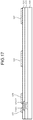
- FIG. 17 is a sectional view illustrating the method for manufacturing the fingerprint sensor according to the first embodiment
- FIG. 18 is a sectional view illustrating the method for manufacturing the fingerprint sensor according to the first embodiment
- FIG. 19 is a sectional view illustrating the method for manufacturing the fingerprint sensor according to the first embodiment
- FIG. 20 is a sectional view illustrating the method for manufacturing the fingerprint sensor according to the first embodiment
- FIG. 21 is a sectional view illustrating the method for manufacturing the fingerprint sensor according to the first embodiment
- FIG. 22 is a sectional view illustrating the method for manufacturing the fingerprint sensor according to the first embodiment
- FIG. 23 is a diagram illustrating a relation between the thickness of an insulating film covering the detection electrodes and the reflectance of light
- FIG. 24 is a plan view illustrating a configuration example of a fingerprint sensor according to a second embodiment
- FIG. 25 is a plan view illustrating the drive electrode and the detection electrode according to the second embodiment.
- FIG. 26 is a diagram omitting the illustration of the detection electrode and an insulating film in FIG. 25 ;
- FIG. 27 is a sectional view illustrating a configuration example of the fingerprint sensor according to the second embodiment.
- FIG. 28 is a sectional view illustrating a method for manufacturing the fingerprint sensor according to the second embodiment
- FIG. 29 is a sectional view illustrating the method for manufacturing the fingerprint sensor according to the second embodiment.
- FIG. 30 is a sectional view illustrating the method for manufacturing the fingerprint sensor according to the second embodiment
- FIG. 31 is a sectional view illustrating the method for manufacturing the fingerprint sensor according to the second embodiment
- FIG. 32 is a sectional view illustrating a configuration example of a fingerprint sensor according to a third embodiment
- FIG. 33 is a sectional view illustrating a configuration example of a fingerprint sensor according to a fourth embodiment
- FIG. 34 is a sectional view illustrating a configuration example of a fingerprint sensor according to a fifth embodiment
- FIG. 35 is a diagram illustrating a relation between the wavelength of light incident on an electrode portion of a drive electrode and the reflectance of light
- FIG. 36 is a sectional view illustrating a configuration example of a fingerprint sensor according to a sixth embodiment
- FIG. 37 is a block diagram illustrating a configuration example of the fingerprint detection device according to a seventh embodiment.
- FIG. 38 is a plan view illustrating a configuration example of the detection electrodes according to the seventh embodiment.
- FIG. 39 is a plan view illustrating a configuration example of the detection electrodes according to the seventh embodiment.
- FIG. 1 is a plan view illustrating a display device according to a first embodiment.
- FIG. 2 is a sectional view obtained by cutting the display device illustrated in FIG. 1 along the A 11 -A 12 line.
- the display device 1 illustrated in FIG. 1 is a display device equipped with a fingerprint detection function and includes: a display region AA for displaying an image; a fingerprint detection region FA; and a frame region GA provided outside the display region AA and the fingerprint detection region FA.
- the fingerprint detection region FA is a region for detecting a recess or protrusion on the surface of a finger or the like being in contact with or in proximity to a cover member 80 .
- the display region AA and the fingerprint detection region FA match with each other or substantially match with each other, thereby enabling detection of a fingerprint across the entire display region AA.
- the shape of the display region AA and that of the fingerprint detection region FA are rectangular, for example.
- the display device 1 of the present embodiment includes a display panel 30 and a fingerprint detection device 100 .
- the fingerprint detection device 100 has a fingerprint sensor 10 and the cover member 80 .
- the cover member 80 is a plate-shaped member having a first surface 80 a and a second surface 80 b on the side opposite of the first surface 80 a .
- the first surface 80 a of the cover member 80 is a detection surface for detecting the recess or protrusion on the surface of the finger or the like being in contact therewith or in proximity thereto, and is also a display surface for allowing an observer to visually recognize an image on the display panel 30 .
- the fingerprint sensor 10 and the display panel 30 are provided on the second surface 80 b side of the cover member 80 .
- the cover member 80 is a member for protecting the fingerprint sensor 10 and the display panel 30 and covers the fingerprint sensor 10 and the display panel 30 .
- the cover member 80 is a glass substrate or a resin substrate, for example.
- the shapes of the cover member 80 , the fingerprint sensor 10 , and the display panel 30 are not limited to be rectangular in a plan view, and may be circular, oval, or an odd shape with part of these outer shape lacked.
- the shape of the cover member 80 is not limited to be plate-shaped.
- the display region AA and the fingerprint detection region FA each have a curved surface or the frame region GA has a curved surface curving toward the display panel 30 , for example, the cover member 80 may have a curved surface.
- the display device is a curved surface display having a fingerprint detection function and can detect a fingerprint also on the curved surface of the curved surface display.
- a “plan view” indicates a case when viewed from a direction perpendicular to one surface 101 a of a substrate 101 illustrated in FIG. 3 described below.
- the direction perpendicular to the one surface 101 a is a “normal direction Dz of the substrate 101 ”.
- a decorative layer 81 is provided on the second surface 80 b of the cover member 80 .
- the decorative layer 81 is a coloring layer, light transmittance of which is lower than that of the cover member 80 .
- the decorative layer 81 can prevent wiring, circuits, and the like provided superimposed on the frame region GA from being visually recognized by the observer.
- the decorative layer 81 is provided on the second surface 80 b , but it may be provided on the first surface 80 a .
- the decorative layer 81 is not limited to be a single layer and may have a multilayered configuration.
- the fingerprint sensor 10 is a detector for detecting a recess or protrusion on the surface of a finger Fin or the like being in contact with or in proximity to the first surface 80 a of the cover member 80 . As illustrated in FIG. 2 , the fingerprint sensor 10 is provided between the cover member 80 and the display panel 30 . When viewed from a direction perpendicular to the first surface 80 a (a normal direction), the fingerprint sensor 10 overlaps with the fingerprint detection region FA and part of the frame region GA. A flexible substrate 76 is connected to the fingerprint sensor 10 in the frame region GA. An integrated circuit (IC) for detection (not illustrated) for controlling detection operations of the fingerprint sensor 10 is mounted on the flexible substrate 76 .
- IC integrated circuit
- One surface of the fingerprint sensor 10 is stuck to the second surface 80 b of the cover member 80 with an adhesive layer 71 , whereas the other surface thereof is stuck to a polarizing plate 35 of the display panel 30 with an adhesive layer 72 .
- Each of the adhesive layer 71 and the adhesive layer 72 is an adhesive or a resin having translucency, and allows visible light to pass therethrough.
- the display panel 30 includes: a pixel substrate 30 A; a counter substrate 30 B; a polarizing plate 34 provided below the pixel substrate 30 A; and the polarizing plate 35 provided above the counter substrate 30 B.
- An IC for display (not illustrated) for controlling a display operation of the display panel 30 is connected to the pixel substrate 30 A via a flexible substrate 75 .
- the display panel 30 is a liquid crystal panel in which a liquid crystal element is used as a display function layer.
- the present disclosure is not limited to this example, and the display panel 30 may be an organic EL display panel, for example.
- the IC for detection and the IC for display described above may be provided on a control substrate outside a module. Alternatively, the IC for detection may be provided on the substrate 101 of the fingerprint sensor 10 (refer to FIG. 3 and FIG. 14 ).
- the IC for display may be provided on a first substrate 31 of the pixel substrate 30 A (refer to FIG. 8 ).
- FIG. 3 is a plan view illustrating a configuration example of the fingerprint detection device according to the first embodiment.
- the fingerprint detection device 100 includes the substrate 101 and the fingerprint sensor 10 provided on the one surface 101 a side of the substrate 101 .
- the fingerprint sensor 10 includes drive electrodes Tx and detection electrodes Rx provided on the one surface 101 a side of the substrate 101 .
- the substrate 101 is a glass substrate having translucency allowing visible light to pass therethrough.
- the substrate 101 may be a translucent resin substrate or a resin film formed of a resin such as polyimide.
- the fingerprint sensor 10 is a sensor having translucency.
- the drive electrodes Tx are formed of a translucent conductive material such as indium tin oxide (ITO).
- the drive electrodes Tx are arranged in a first direction Dx.
- the drive electrodes Tx extend in a second direction Dy intersecting (e.g., orthogonal to) the first direction Dx.
- the detection electrodes Rx are arranged in the second direction Dy.
- the detection electrodes Rx extend in the first direction Dx. In this manner, the detection electrodes Rx extend in a direction intersecting the extension direction of the drive electrodes Tx.
- the detection electrodes Rx are each connected to the flexible substrate 75 provided on a short side of the frame region GA of the substrate 101 via frame wiring (not illustrated).
- the drive electrodes Tx employ a conductive material having translucency such as ITO. As illustrated in FIG. 3 , the drive electrodes Tx and the detection electrodes Rx are provided in the fingerprint detection region FA.
- Capacitance is formed at each of intersections between the detection electrodes Rx and the drive electrodes Tx.
- a drive electrode driver 15 sequentially selects the drive electrodes Tx in a time division manner, and supplies a drive signal Vs to the selected drive electrode Tx.
- a detection signal Vdet corresponding to a capacitance change by the recess or protrusion on the surface of the finger or the like being in contact with or in proximity to the cover member 80 is output from the detection electrodes Rx, whereby fingerprint detection is performed.
- the drive electrode driver 15 may sequentially select each drive electrode block including a plurality of drive electrodes Tx and drive the drive electrodes Tx.
- FIG. 3 illustrates a case in which the various kinds of circuits such as a detection electrode selection circuit 14 and the drive electrode driver 15 are provided in the frame region GA of the substrate 101 , this is a mere example. At least part of the various kinds of circuits may be included in the IC for detection mounted on the flexible substrate 76 .
- FIG. 4 is a block diagram illustrating a configuration example of the fingerprint detection device including the fingerprint sensor.
- the fingerprint detection device 100 includes the fingerprint sensor 10 , a detection controller 11 , the drive electrode driver 15 , the detection electrode selection circuit 14 , and a detector 40 .
- the detection controller 11 is a circuit for controlling detection operations of the fingerprint sensor 10 .
- the drive electrode driver 15 is a circuit for supplying a drive signal Vs for detection to the drive electrodes Tx of the fingerprint sensor 10 based on a control signal supplied from the detection controller 11 .
- the detection electrode selection circuit 14 selects the detection electrodes Rx of the fingerprint sensor 10 based on a control signal supplied from the detection controller 11 to connect the selected detection electrodes Rx to the detector 40 .
- the detector 40 is a circuit for detecting the recess or protrusion on the surface of the finger or the like being in contact with or in proximity to the first surface 80 a of the cover member 80 based on a control signal supplied from the detection controller 11 and the detection signal Vdet output from an insulating film 150 to detect the shape of a fingerprint.
- the detector 40 includes a detection signal amplifier 42 , an analog-to-digital (A/D) converter 43 , a signal processor 44 , a coordinates extractor 45 , a synthesizer 46 , and a detection timing controller 47 .
- the detection timing controller 47 performs control to cause the detection signal amplifier 42 , the A/D converter 43 , the signal processor 44 , the coordinates extractor 45 , and the synthesizer 46 to operate in synchronization with each other based on a control signal supplied from the detection controller 11 .
- the detection signal Vdet is supplied to the detection signal amplifier 42 of the detector 40 from the fingerprint sensor 10 .
- the detection signal amplifier 42 amplifies the detection signal Vdet.
- the A/D converter 43 converts an analog signal output from the detection signal amplifier 42 into a digital signal.
- the signal processor 44 is a logic circuit for detecting whether the finger is in contact with or in proximity to the fingerprint sensor 10 based on an output signal of the A/D converter 43 .
- the signal processor 44 performs processing to extract a differential signal of detection signals (an absolute value
- the signal processor 44 compares the absolute value
- the coordinates extractor 45 is a logic circuit that, when the contact or proximity of the finger is detected by the signal processor 44 , determines its detected coordinates.
- the coordinates extractor 45 outputs the detected coordinates to the synthesizer 46 .
- the synthesizer 46 combines the detection signal Vdet output from the fingerprint sensor 10 to generate two-dimensional information indicating the shape of the finger being in contact with or in proximity to the fingerprint sensor 10 .
- the synthesizer 46 outputs the two-dimensional information as output Vout of the detector 40 .
- the synthesizer 46 may generate an image based on the two-dimensional information and make image information serve as the output Vout.
- the IC for detection described above functions as the detector 40 illustrated in FIG. 4 .
- Part of the functions of the detector 40 may be included in the IC for display described above or be provided as functions of an external micro-processing unit (MPU).
- MPU micro-processing unit
- the fingerprint sensor 10 operates based on the basic principle of capacitance type detection.
- the following describes the basic principle of mutual capacitance detection by the fingerprint sensor 10 with reference to FIG. 5 to FIG. 7 .
- FIG. 5 is a diagram for explaining the basic principle of mutual capacitance detection.
- FIG. 6 is a diagram illustrating an exemplary equivalent circuit for explaining the basic principle of the mutual capacitance detection.
- FIG. 7 is a diagram illustrating exemplary waveforms of a drive signal and a detection signal of the mutual capacitance detection. While the following describes a case in which a finger is in contact with or in proximity to a detection electrode, the present disclosure is not limited to the finger, and a target may be an object including a conductor such as a stylus, for example.
- a capacitance element C 1 includes a pair of electrodes facing each other across a dielectric D, i.e., a drive electrode E 1 , and a detection electrode E 2 .
- the capacitance element C 1 produces lines of electric force for a fringe extending from ends of the drive electrode E 1 toward an upper surface of the detection electrode E 2 in addition to lines of electric force (not illustrated) generated between opposing surfaces of the drive electrode E 1 and the detection electrode E 2 .
- one end of the capacitance element C 1 is connected to an AC signal source (a drive signal source) S, whereas the other end thereof is connected to a voltage detector DET.
- the voltage detector DET is an integral circuit included in the detector 40 illustrated in FIG. 4 , for example.
- the AC signal source S applies an AC rectangular wave Sg at a predetermined frequency (e.g., a frequency of several kilohertz to several hundred kilohertz) to the drive electrode E 1 (one end of the capacitance element C 1 ), an output waveform (the detection signal Vdet) as illustrated in FIG. 7 appears via the voltage detector DET connected to the detection electrode E 2 (the other end of the capacitance element C 1 ).
- the AC rectangular wave Sg corresponds to the drive signal Vs input from the drive electrode driver 15 illustrated in FIG. 4 .
- a current corresponding to the capacitance value of the capacitance element C 1 flows with charge and discharge of the capacitance element C 1 .
- the voltage detector DET illustrated in FIG. 6 converts fluctuations in a current I 1 corresponding to the AC rectangular wave Sg into fluctuations in voltage (a solid line waveform V 1 (refer to FIG. 7 )).
- the waveform V 2 is smaller in amplitude than the waveform V 1 described above.
- of a voltage difference between the waveform V 1 and the waveform V 2 changes in accordance with the influence of an external object being in contact with or in proximity to the detection electrode E 2 from the outside such as a finger.
- the voltage detector DET preferably operates with a period Reset to reset charge and discharge of a capacitor in accordance with the frequency of the AC rectangular wave Sg by switching in the circuit.
- the detector 40 compares the absolute value
- the drive electrode E 1 illustrated in FIG. 5 corresponds to the drive electrode Tx illustrated in FIG. 3
- the detection electrode E 2 illustrated in FIG. 5 corresponds to the detection electrode Rx illustrated in FIG. 3 .
- FIG. 8 is a sectional view illustrating a configuration example of a display panel.
- the pixel substrate 30 A includes a first substrate 31 , pixel electrodes 32 , and a common electrode 33 .
- the common electrode 33 is provided on the first substrate 31 .
- the pixel electrodes 32 are provided above the common electrode 33 via an insulating layer 38 , and are arranged in a matrix (row-column configuration) in a plan view.
- the pixel electrodes 32 are provided corresponding to respective subpixels forming each pixel Pix of the display panel 30 , and are supplied with pixel signals for performing a display operation.
- the common electrode 33 to which DC drive signals for display are supplied, functions as a common electrode for the pixel electrodes 32 .
- the common electrode 33 , the insulating layer 38 , and the pixel electrodes 32 are stacked in this order on the first substrate 31 .
- the polarizing plate 34 is provided below the first substrate 31 via an adhesive layer.
- Thin film transistors (TFT, not illustrated) serving as switching elements for display are provided to the first substrate 31 .
- a conductive material having translucency such as ITO is used for the pixel electrodes 32 and the common electrode 33 .
- the arrangement of the pixel electrodes 32 is not limited to the matrix arrangement in which the pixel electrodes 32 are arranged in a first direction and a second direction orthogonal to the first direction, and may employ an arrangement in which adjacent pixel electrodes 32 are shifted from each other in the first direction or the second direction.
- the present disclosure can employ a configuration in which, with respect to one pixel electrode 32 constituting a pixel column in the first direction, two or three pixel electrodes 32 are arranged on one side of the one pixel electrode 32 , according to a difference in shape between adjacent pixel electrodes 32 .
- the counter substrate 30 B includes a second substrate 36 and a color filter 37 formed on one surface of the second substrate 36 .
- the color filter 37 faces a liquid crystal layer 6 in a direction perpendicular to the first substrate 31 .
- the polarizing plate 35 is provided above the second substrate 36 via an adhesive layer.
- the color filter 37 may be arranged on the first substrate 31 .
- each of the first substrate 31 and the second substrate 36 is a glass substrate or a resin substrate, for example.
- the liquid crystal layer 6 is provided between the first substrate 31 and the second substrate 36 .
- the liquid crystal layer 6 modulates light passing therethrough in accordance with the state of an electric field, and employs liquid crystals in a transverse electric field mode such as an in-plane switching (IPS) mode including a fringe field switching (FFS) mode.
- An orientation film may be provided between the liquid crystal layer 6 and the pixel substrate 30 A and between the liquid crystal layer 6 and the counter substrate 30 B illustrated in FIG. 8 .
- the illuminator (a backlight, not illustrated) is provided below the first substrate 31 .
- the illuminator has a light source such as a light-emitting diode (LED), for example, and emits light from the light source toward the first substrate 31 .
- the light from the illuminator passes through the pixel substrate 30 A, and switching is performed between part of the light to be blocked and not to be emitted and part of the light to be emitted depending on the state of liquid crystals, so that an image is displayed on the display surface (the first surface 80 a ).
- the display panel 30 is stuck to the fingerprint sensor 10 via the adhesive layer 72 provided on the polarizing plate 35 in the display region AA.
- the fingerprint sensor 10 is arranged at a position closer to the cover member 80 than the display panel 30 is to the cover member 80 in a direction orthogonal to the second surface 80 b of the cover member 80 .
- the provision of the fingerprint sensor 10 closer to the cover member 80 can reduce a distance between the detection electrodes Rx and the first surface 80 a serving as the detection surface, in comparison with a case in which detection electrodes for fingerprint detection are provided integrally with the display panel 30 , for example. Consequently, the display device 1 of the present embodiment can improve detection performance.
- FIG. 9 is a plan view illustrating a configuration example of detection electrodes of the fingerprint sensor according to the first embodiment.
- the detection electrodes Rx intersect the drive electrodes Tx.
- the shape of the detection electrode Rx is a zigzag line.
- the detection electrodes Rx zigzag in the first direction Dx.
- the detection electrodes Rx each have a plurality of first line portions RxL 1 , a plurality of second line portions RxL 2 , and a plurality of bent portions RxB, for example.
- the second line portions RxL 2 extend in a direction intersecting the first line portions RxL 1 .
- the bent portions RxB connect the first line portions RxL 1 and the second line portions RxL 2 to each other.
- first line portions RxL 1 extend in a direction intersecting the first direction Dx and the second direction Dy.
- the second line portions RxL 2 also extend in a direction intersecting the first direction Dx and the second direction Dy.
- the first line portions RxL 1 and the second line portions RxL 2 are arranged so as to be bilaterally symmetric about a virtual line (not illustrated) parallel to the first direction Dx.
- an arrangement pitch of bent portions RxB in th first direction Dx is defined as Prx.
- an arrangement pitch of the bent portions RxB in the second direction Dy is defined as Pry.
- a magnitude relation of Pry ⁇ Prx holds, for example.
- An arrangement pitch of the drive electrodes Tx in the first direction Dx is defined as Pt.
- An arrangement pitch in the first direction Dx of the pixel electrodes 32 of the display panel 30 stuck to the fingerprint detection device 100 is defined as Ppix.
- a magnitude relation of the arrangement pitch Pt of the drive electrodes Tx and the arrangement pitch Ppix of the pixel electrodes 32 preferably satisfies the following Expression (1), where n is an integer of 1 or more. With this relation, the fingerprint sensor 10 can reduce the occurrence of unintended patterns (e.g., moire and a light reflecting pattern) in the fingerprint detection region FA. 0.6 ⁇ ( n ⁇ 1) ⁇ Ppix ⁇ Pt ⁇ 0.4 ⁇ n ⁇ Ppix (1)
- An arrangement pitch of the connecting portions 127 in the first direction Dx is defined as Pb.
- the arrangement pitch Pb of the connecting portions 127 is preferably 0.5 times the arrangement pitch Pt of the drive electrode Tx.
- the connecting portions 127 are preferably arranged alternately on one side and the other side relative to a central line Lcent parallel to the second direction Dy and passing through the center of the electrode portions 130 .
- the connecting portions 127 light transmittance of which is lower than that of the electrode portions 130 , are not arranged on a straight line, so that the fingerprint sensor 10 can reduce the occurrence of unintended patterns such as moire.
- the longitudinal directions of the connecting portions 127 are preferably aligned in one direction. All of the longitudinal directions of the connecting portions 127 of the drive electrodes Tx are the second direction, for example. This structure uniforms the shape of the connecting portions 127 intersecting the detection electrodes Rx, which makes it easy to uniform capacitance between the drive electrodes Tx and the connecting portions 127 .
- the shape of the drive electrodes Tx, the shape of the detection electrodes Rx, and the positional relation thereof are uniform among the electrodes, and thus variations in capacitance of the drive electrodes Tx and variations in capacitance of the detection electrodes Rx are small. Further, there is an advantage that the calculation of coordinates in the fingerprint sensor 10 is easily corrected, for example.
- FIG. 11 is a plan view illustrating a drive electrode and a detection electrode according to the first embodiment.
- FIG. 12 is a diagram omitting the illustration of the electrode portions and the detection electrode in FIG. 11 .
- an insulating layer 129 is arranged between the connecting portion 127 and the detection electrode Rx.
- the insulating layer 129 is a resin insulating film, for example.
- the insulating layer 129 includes a first insulating film 129 A and a second insulating film 129 B thinner than the first insulating film 129 A.
- the second insulating film 129 B is provided with a contact hole 129 H.
- the connecting portion 127 is exposed at the bottom of the contact hole 129 H.
- FIG. 13 is a plan view illustrating a configuration example of the electrode portions.
- the electrode portion 130 has an electrode main body 131 and a protruding portion 132 in a plan view protruding toward an adjacent electrode portion 130 from the electrode main body 131 .
- the second insulating film 129 B is arranged between the protruding portion 132 and the connecting portion 127 .
- the protruding portion 132 is embedded in the contact hole 129 H (refer to FIG. 11 ) provided in the second insulating film 129 B. With this structure, the protruding portion 132 is connected to the connecting portion 127 (refer to FIG. 11 ) via the contact hole 129 H.
- the electrode portions 130 are connected to each other in the second direction Dy via the connecting portions 127 .
- the detection electrode Rx is arranged so as to overlap with the protruding portions 132 and capacitance generated between the electrode portions 130 and the detection electrode Rx can be reduced, in comparison with a case in which the electrode main bodies 131 and the detection electrode Rx overlap with each other.
- the electrode portions 130 when viewed from the normal direction Dz, have a plurality of shapes.
- the electrode portions 130 include a first electrode portion 130 A and a second electrode portion 130 B, the shape of the electrode main body 131 (refer to FIG. 13 ) of which is different from that of the first electrode portion 130 A.
- each of the shape of the electrode main body 131 of the first electrode portion 130 A and the shape of the electrode main body 131 of the second electrode portion 130 B is a parallelogram.
- the shape of the electrode main body 131 of the first electrode portion 130 B is obtained by vertically flipping the shape of the electrode main body 131 of the second electrode portion 130 A.
- the drive electrodes Tx- 1 and Tx- 2 intersecting the first line portions RxL 1 of the detection electrodes Rx include the first electrode portion 130 A having two sides parallel to the first line portions RxL 1 .
- the drive electrodes Tx- 3 and Tx- 4 intersecting the second line portions RxL 2 of the detection electrodes Rx include the second electrode portion 130 B having two sides parallel to the second line portions RxL 2 .
- the electrode main bodies 131 when viewed from the normal direction Dz, the electrode main bodies 131 can be arranged along the zigzag detection electrode Rx, and a separating distance d 3 between the zigzag detection electrode Rx and the electrode main bodies 131 can be a constant length.
- FIG. 14 is a sectional view illustrating a configuration example of the fingerprint sensor.
- the section of the fingerprint detection region FA is obtained by cutting the plan view illustrated in FIG. 10 along the A 13 -A 14 line.
- the section of the frame region GA is obtained by cutting a part including a thin film transistor Tr of the drive electrode driver 15 (refer to FIG. 3 ).
- FIG. 14 illustrates the section along the A 13 -A 14 line of the fingerprint detection region FA and the section of the part including the thin film transistor Tr of the frame region GA by schematically connecting these parts in order to show a relation between the layer structure of the fingerprint detection region FA and the layer structure of the frame region GA.
- the fingerprint sensor 10 has the substrate 101 , a gate electrode 103 provided on the substrate 101 , and a first inter-layer insulating film 111 provided on the substrate 101 to cover the gate electrode 103 .
- the gate electrode 103 is provided in the frame region GA.
- Aluminum (Al), copper (Cu), silver (Ag), molybdenum (Mo), or an alloy of these materials is used as the material of the gate electrode 103 .
- a silicon oxide film, a silicon nitride film, or a silicon oxide nitride film is used as the material of the first inter-layer insulating film 111 .
- the first inter-layer insulating film 111 is not limited to a single layer and may be a film with a multilayered structure.
- the first inter-layer insulating film 111 may be a film with a multilayered structure in which a silicon nitride film is formed on a silicon oxide film, for example.
- the fingerprint sensor 10 includes: a semiconductor layer 113 formed on the first inter-layer insulating film 111 ; and a second inter-layer insulating film 121 formed on the first inter-layer insulating film 111 to cover the semiconductor layer 113 .
- the second inter-layer insulating film 121 is provided with contact holes 121 H 1 and 121 H 2 .
- the semiconductor layer 113 is exposed at the bottom of the contact holes 121 H 1 and 121 H 2 .
- a polysilicon or an oxide semiconductor is used as the material of the semiconductor layer 113 .
- a silicon oxide film, a silicon nitride film, or a silicon oxide nitride film is used as the material of the second inter-layer insulating film 121 .
- the second inter-layer insulating film 121 is not limited to a single layer and may be a film with a multilayered structure.
- the second inter-layer insulating film 121 may be a film with a multilayered structure in which a silicon nitride film is formed on a silicon oxide film, for example.
- the fingerprint sensor 10 includes a source electrode 123 , a drain electrode 125 , and the connecting portions 127 provided on the second inter-layer insulating film 121 .
- the source electrode 123 is embedded in the contact hole 121 H 1 .
- the drain electrode 125 is embedded in the contact hole 121 H 2 .
- the source electrode 123 is connected to the semiconductor layer 113 via the contact hole 121 H 1 .
- the drain electrode 125 is connected to the semiconductor layer 113 via the contact hole 121 H 2 .
- Titanium aluminum (TiAl) which is an alloy of titanium and aluminum, is used as the materials of the source electrode 123 , the drain electrode 125 , and the connecting portions 127 .
- the gate electrode 103 , the semiconductor layer 113 , the source electrode 123 , and the drain electrode 125 described above are provided in the frame region GA.
- the gate electrode 103 , the semiconductor layer 113 , the source electrode 123 , and the drain electrode 125 constitute the thin film transistor Tr in the frame region GA.
- the insulating layer 129 is provided on the second inter-layer insulating film 121 .
- the insulating layer 129 includes the first insulating film 129 A and the second insulating film 129 B thinner than the first insulating film 129 A.
- the first insulating film 129 A provided in the frame region GA covers the source electrode 123 and the drain electrode 125 .
- the first insulating film 129 A provided in the frame region GA is provided with the contact hole 129 H.
- the first insulating film 129 A provided in the fingerprint detection region FA covers part of the connecting portion 127 positioned under the detection electrode Rx.
- the second insulating film 129 B provided in the fingerprint detection region FA covers part of the connecting portion 127 positioned under the electrode portion 130 .
- the second insulating film 129 B is provided with the contact hole 129 H.
- a resin film is used as the insulating layer 129 , for example. Since the resin film has a high refractive index, the resin film serving as the insulating layer 129 is preferably not arranged in the display region AA as much as possible. Not arranging the resin film in the display region AA as much as possible improves the visibility of an image displayed on the display region AA. As described above, in the display device 1 of the present embodiment, the display region AA and the fingerprint detection region FA match with each other or substantially match with each other. In the configuration in FIG. 14 , only the second insulating film 129 B, which is a thin film, is arranged as the insulating layer 129 in the display region AA. Consequently, the visibility of the image displayed on the display region AA improves.
- the electrode portions 130 are provided on the second inter-layer insulating film 121 .
- the peripheral parts of the electrode portions 130 e.g., the protruding portions 132 illustrated in FIG. 13
- the electrode portions 130 are connected to the connecting portions 127 via the contact hole 129 H.
- the electrode portions 130 are in contact with the second inter-layer insulating film 121 .
- the detection electrodes Rx are provided on the first insulating film 129 A.
- the first insulating film 129 A insulates the detection electrodes Rx and the drive electrodes Tx from each other.
- the detection electrode Rx includes a first metallic layer 141 , a second metallic layer 142 , and a third metallic layer 143 , for example.
- the second metallic layer 142 is provided on the third metallic layer 143
- the first metallic layer 141 is provided on the second metallic layer 142 .
- Molybdenum or a molybdenum alloy is used as the materials of the first metallic layer 141 and the third metallic layer 143 , for example.
- Aluminum or an aluminum alloy is used as the material of the second metallic layer 142 .
- Molybdenum or a molybdenum alloy forming the first metallic layer 141 has a reflectance of visible light lower than that of aluminum or an aluminum alloy forming the second metallic layer 142 .
- the insulating film 150 is provided above the insulating layer 129 , the electrode portions 130 , and the detection electrodes Rx.
- the insulating film 150 covers upper surfaces and side surfaces of the detection electrodes Rx.
- a film with a high refractive index and a low reflectance such as a silicon nitride film is used as the insulating film 150 .
- the insulating film 150 may be a light-shielding resin film (e.g., a black resin film).
- FIG. 15 to FIG. 22 are sectional views each illustrating a method for manufacturing the fingerprint sensor according to the first embodiment.
- a manufacturing apparatus (not illustrated) forms a conductive film (not illustrated) such as aluminum on the substrate 101 .
- the conductive film is formed by sputtering, for example.
- the manufacturing apparatus forms the gate electrode 103 by patterning the conductive film by photolithography technique and dry etching technique.
- the manufacturing apparatus forms a resist (not illustrated) on the conductive film, for example.
- the resist which is patterned by the photolithography, is formed into a shape covering an area in which the gate electrode 103 is formed, and exposing the other area.
- the manufacturing apparatus removes the conductive film in the area exposed from the resist by the dry etching technique. With this operation, the gate electrode 103 is formed out of the conductive film. After forming the gate electrode 103 , the manufacturing apparatus removes the resist.
- the manufacturing apparatus forms the first inter-layer insulating film 111 on the substrate 101 .
- the first inter-layer insulating film 111 is formed by chemical vapor deposition (CVD), for example. With this operation, the gate electrode 103 is covered with the first inter-layer insulating film 111 .
- the manufacturing apparatus forms a semiconductor film (not illustrated) on the first inter-layer insulating film 111 .
- the semiconductor film is formed by the CVD, for example.
- the manufacturing apparatus patterns the semiconductor film by the photolithography technique and the dry etching technique. With this operation, the manufacturing apparatus forms the semiconductor layer 113 out of the semiconductor film.
- the manufacturing apparatus forms the second inter-layer insulating film 121 on the first inter-layer insulating film 111 .
- the second inter-layer insulating film 121 is formed by the CVD, for example. With this operation, the semiconductor layer 113 is covered with the second inter-layer insulating film 121 .
- the manufacturing apparatus forms the contact holes 121 H 1 and 121 H 2 in the second inter-layer insulating film 121 .
- the manufacturing apparatus forms a resist (not illustrated) on the second inter-layer insulating film 121 , for example.
- the resist which is patterned by the photolithography, is formed into a shape exposing areas in which the contact holes 121 H 1 and 121 H 2 are formed, and covering the other area.
- the manufacturing apparatus removes the second inter-layer insulating film 121 in the area exposed from the resist by the dry etching technique. With this operation, the contact holes 121 H 1 and 121 H 2 are formed in the second inter-layer insulating film 121 .
- the manufacturing apparatus removes the resist.
- the manufacturing apparatus forms a metallic film (not illustrated) such as titanium aluminum on the second inter-layer insulating film 121 .
- the metallic film is formed by the sputtering, for example.
- the manufacturing apparatus patterns the metallic film by the photolithography technique and the dry etching technique. With this operation, as illustrated in FIG. 17 , the manufacturing apparatus forms the source electrode 123 , the drain electrode 125 , and the connecting portions 127 out of the metallic film.
- the manufacturing apparatus forms the insulating layer 129 on the second inter-layer insulating film 121 .
- the insulating layer 129 is a resin film, for example, and is a positive resist, for example.
- the insulating layer 129 is formed by spin coating technique, for example.
- the insulating layer 129 covers the source electrode 123 , the drain electrode 125 , and the connecting portions 127 .
- the manufacturing apparatus performs first exposure processing on the insulating layer 129 .
- the first exposure processing is half exposure. As illustrated in FIG. 19 , in the half exposure, part of the insulating layer 129 ranging from an upper surface of the insulating layer 129 to a halfway position exp in the thickness direction of the insulating layer 129 is exposed. Subsequently, the manufacturing apparatus performs second exposure processing on the insulating layer 129 . With this operation, the part of the insulating layer 129 in which the contact hole 129 H (refer to FIG. 14 ) is formed is exposed.
- the manufacturing apparatus performs developing processing on the insulating layer 129 .
- the developing processing the part exposed through the first exposure processing and the part exposed through the second exposure processing are removed from the insulating layer 129 . Consequently, as illustrated in FIG. 20 , the first insulating film 129 A and the second insulating film 129 B thinner than the first insulating film 129 A are formed out of the insulating layer 129 .
- the contact hole 129 H is formed in the second insulating film 129 B.
- the manufacturing apparatus forms a conductive film such as ITO (not illustrated) above the substrate 101 .
- the conductive film is formed by the sputtering, for example.
- the manufacturing apparatus patterns the conductive film by the photolithography technique and the dry etching technique. With this operation, as illustrated in FIG. 21 , the manufacturing apparatus forms the electrode portions 130 out of the conductive film.
- the manufacturing apparatus forms a metallic film with a multilayered structure (not illustrated) above the substrate 101 .
- the metallic film with the multilayered structure is a film with molybdenum or a molybdenum alloy, aluminum or an aluminum alloy, and molybdenum or a molybdenum alloy stacked in this order from the substrate 101 , for example.
- the metallic film is formed by the sputtering, for example.
- the manufacturing apparatus patterns the metallic film by the photolithography technique and the dry etching technique. With this operation, as illustrated in FIG. 22 , the manufacturing apparatus forms the detection electrode Rx including the first metallic layer 141 , the second metallic layer 142 , and the third metallic layer 143 .
- the manufacturing apparatus forms the insulating film 150 (refer to FIG. 14 ) above the substrate 101 .
- the insulating film 150 is formed by the CVD or the like.
- the fingerprint sensor 10 includes the drive electrodes Tx and the detection electrodes Rx both provided on the one surface 101 a side of the substrate 101 .
- the drive electrodes Tx are arranged in the first direction Dx.
- the detection electrodes Rx are arranged in the second direction Dy intersecting the first direction Dx.
- the fingerprint sensor 10 includes the insulating layer 129 provided in the normal direction Dz of the substrate 101 between the drive electrodes Tx and the respective detection electrodes Rx. In the normal direction of the substrate 101 , the detection electrodes Rx intersect the drive electrodes Tx.
- the detection electrode Rx has the first metallic layer 141 and the second metallic layer 142 positioned closer to the one surface 101 a than the first metallic layer 141 is to the one surface 101 a .
- the first metallic layer 141 has a reflectance of visible light lower than that of the second metallic layer 142 .
- This structure can reduce the reflection of light coming from the cover member 80 side (hereinafter, incident light) on the detection electrodes Rx, thereby making the detection electrodes Rx less noticeable. Consequently, the fingerprint sensor 10 can reduce the occurrence of unintended patterns such as moire.
- the fingerprint sensor 10 includes the insulating film 150 provided on the one surface 101 a side of the substrate 101 .
- the insulating film 150 covers the detection electrodes Rx.
- the insulating film 150 is a film with a high refractive index and a low reflectance and is a silicon nitride film, for example.
- the insulating film 150 is a light-shielding resin film (e.g., a black resin film). With this structure, the fingerprint sensor 10 can further reduce the reflection of light.
- FIG. 23 is a diagram illustrating a relation between the thickness of an insulating film covering the detection electrodes and the reflectance of light.
- the horizontal axis of FIG. 23 indicates a wavelength (nm) of light incident on the fingerprint detection region FA, where 380 nm to 780 nm correspond to a wavelength range of visible light.
- the vertical axis of FIG. 23 indicates the reflectance of light coming from the detection electrodes Rx.
- Dre 1 is measured data when no silicon nitride film is provided on the detection electrodes Rx so that the detection electrodes Rx are exposed to the air.
- Dre 2 is measured data when a silicon nitride film with a thickness of 100 nm is provided on the detection electrodes Rx.
- Dre 3 is measured data when a silicon nitride film with a thickness of 50 nm is provided on the detection electrodes Rx. As illustrated in FIG. 23 , in the wavelength range of visible light, the data Dre 2 and Dre 3 have a reflectance lower than that of the data Dre 1 . Consequently, the fingerprint sensor 10 can further reduce the reflection of light by having the insulating film 150 . As illustrated in FIG. 23 , there is a correlation between the thickness of the silicon nitride film and the reflectance of visible light. Consequently, a designer of the fingerprint detection device may set the thickness of the insulating film 150 so as to make the reflectance of visible light a desired value.
- the electrode portions 130 are translucent electrodes, whereas the detection electrodes Rx are metallic thin lines. This structure can reduce resistance and capacitance of the detection electrodes Rx.
- the detection electrodes Rx are metallic thin lines and are thus small in electrode width. This structure can reduce the area covered with the detection electrodes Rx. Consequently, the fingerprint sensor 10 can increase the aperture of the fingerprint detection region FA and increase the translucency of the fingerprint detection region FA.
- the insulating layer 129 includes: the first insulating film 129 A arranged between the connecting portion 127 and the detection electrode Rx in the normal direction Dz of the substrate 101 ; and the second insulating film 129 B arranged between the connecting portion 127 and the electrode portion 130 .
- the second insulating film 129 B is thinner than the first insulating film 129 A.
- This structure allows the fingerprint sensor 10 to reduce a level difference of the electrode portion 130 in comparison with a case in which the electrode portion 130 is arranged on the first insulating film 129 A. This structure can lower the probability of disconnection in the electrode portion 130 .
- the first insulating film 129 A arranged between the connecting portion 127 and the detection electrode Rx is larger in thickness than the second insulating film 129 B, and thus can reduce capacitance generated between the detection electrodes Rx and the drive electrodes Tx.
- the fingerprint sensor 10 includes: the first inter-layer insulating film 111 provided on the one surface 101 a of the substrate 101 ; and the second inter-layer insulating film 121 provided on the first inter-layer insulating film 111 in the fingerprint detection region FA.
- the drive electrodes Tx are provided on the second inter-layer insulating film.
- the sum of the thickness of the first inter-layer insulating film 111 , the thickness of the second inter-layer insulating film 121 , and the thickness of the drive electrode Tx is preferably 150 nm or less. This structure can reduce the reflection of light incident on the drive electrodes Tx.
- the connecting portion 127 may be connected to the electrode portion 130 without via a contact hole.
- the electrode portions 130 adjacent to each other in the second direction Dy may be connected to each other via a conductive film formed simultaneously with the electrode portions 130 at the same process.
- FIG. 24 is a plan view illustrating a configuration example of a fingerprint sensor according to a second embodiment.
- FIG. 25 is a plan view illustrating the drive electrode and the detection electrode according to the second embodiment.
- FIG. 26 is a diagram omitting the illustration of the detection electrode and the insulating film in FIG. 25 .
- FIG. 27 is a sectional view illustrating a configuration example of the fingerprint sensor according to the second embodiment.
- one drive electrode Tx has a plurality of electrode portions 130 , a plurality of connecting portions (hereinafter, first connecting portions) 127 , and a plurality of second connecting portions 133 .
- the electrode portions 130 are arranged in the second direction Dy and are spaced apart from each other.
- the first connecting portions 127 and the second connecting portions 133 each connect adjacent electrode portions among the electrode portions 130 to each other.
- the second connecting portion 133 is provided above the first connecting portion 127 .
- the second connecting portion 133 is a film formed simultaneously with the electrode portions 130 at the same process.
- the second connecting portion 133 is integral with the electrode portions 130 .
- An insulating film 135 is provided between the second connecting portion 133 and the detection electrode Rx. With this structure, the detection electrodes Rx and the drive electrodes Tx are insulated from each other.
- the insulating film 135 is a resin insulating film, for example.
- FIG. 28 to FIG. 31 are sectional views each illustrating a method for manufacturing the fingerprint sensor according to the second embodiment.
- the method for manufacturing the finger sensor according to the second embodiment is identical to that of the finger sensor according to the first embodiment (refer to FIG. 15 to FIG. 17 ) until the process by which the manufacturing apparatus (not illustrated) forms the source electrode 123 , the drain electrode 125 , and the connecting portion 127 in FIG. 28 .
- the manufacturing apparatus After forming the source electrode 123 , the drain electrode 125 , and the connecting portion 127 , the manufacturing apparatus forms the insulating layer 129 only in the frame region GA, as illustrated in FIG. 29 .
- the manufacturing apparatus forms the contact hole 129 H in the insulating layer 129 .
- the manufacturing apparatus forms an insulating film (not illustrated) above the substrate 101 , for example.
- the insulating film covers the source electrode 123 , the drain electrode 125 , and the connecting portions 127 .
- the manufacturing apparatus performs exposure processing on the insulating film. With this operation, part of the insulating film positioned in the fingerprint detection region FA and part of the insulating film in which the contact hole 129 H is formed are exposed. Subsequently, the manufacturing apparatus performs developing processing on the insulating film to remove the exposed part. With this operation, the manufacturing apparatus forms the insulating layer 129 in the frame region GA and forms the contact hole 129 H in the insulating layer 129 .
- the manufacturing apparatus forms a conductive film such as ITO (not illustrated) above the substrate 101 .
- the conductive film is formed by the sputtering, for example.
- the manufacturing apparatus patterns the conductive film by the photolithography technique and the dry etching technique. With this operation, as illustrated in FIG. 31 , the manufacturing apparatus forms the electrode portion 130 and the second connecting portions 133 out of the conductive film.
- the manufacturing apparatus forms the insulating film 135 only in the fingerprint detection region FA, as illustrated in FIG. 31 .
- the manufacturing apparatus forms an insulating film (not illustrate) above the substrate 101 , for example.
- the insulating film covers the electrode portion 130 and the like.
- the manufacturing apparatus performs exposure processing on the insulating film. With this operation, the insulating film other than part thereof positioned on the second connecting portion 133 is exposed.
- the manufacturing apparatus performs developing process on the insulating film to remove the exposed part. With this operation, the manufacturing apparatus forms the insulating layer 129 on the second connecting portion 133 .
- the manufacturing apparatus forms the detection electrode Rx including the first metallic layer 141 , the second metallic layer 142 , and the third metallic layer 143 on the insulating layer 129 .
- the manufacturing apparatus forms the insulating film 150 (refer to FIG. 27 ) above the substrate 101 .
- the insulating film 150 is formed by the CVD or the like.
- the detection electrode Rx has the first metallic layer 141 and the second metallic layer 142 .
- the first metallic layer 141 has a reflectance of visible light lower than that of the second metallic layer 142 .
- the fingerprint sensor 10 A can reduce the reflection of light by the detection electrodes Rx and can reduce the occurrence of unintended patterns (e.g., moire and a light reflecting pattern) due to this reflection.
- the structure can reduce the size of the connecting portions 127 , and reduce the area covered with the connecting portions 127 .
- the fingerprint sensor 10 A can further increase aperture of the fingerprint detection region FA and further increase the translucency of the fingerprint detection region FA.
- FIG. 32 is a sectional view illustrating a configuration example of a fingerprint sensor according to a third embodiment.
- the insulating layer 129 is arranged between the substrate 101 and the electrode portion 130 in the fingerprint detection region FA.
- the insulating layer 129 is arranged on the second inter-layer insulating film 121 , and the electrode portion 130 is arranged on the insulating layer 129 , for example.
- the process of arranging the insulating layer 129 on the substrate 101 in the fingerprint detection region FA may be performed by masking a region excluding the insulating layer 129 so as not to cause light incident on the region in the exposure processing for the insulating layer 129 described with reference to FIG. 29 . With this operation, the insulating layer 129 is arranged on the substrate 101 .
- the detection electrode Rx has the first metallic layer 141 and the second metallic layer 142 .
- the first metallic layer 141 has a reflectance of visible light lower than that of the second metallic layer 142 .
- the process of removing the first insulating film 129 A described above (refer to FIG. 14 ) is eliminated, and the number of processes of manufacturing the fingerprint sensor 10 B can be reduced in comparison with that of the fingerprint sensor 10 A (refer to FIG. 14 ).
- FIG. 33 is a sectional view illustrating a configuration example of a fingerprint sensor according to a fourth embodiment.
- the first inter-layer insulating film 111 and the second inter-layer insulating film 121 are not arranged between the substrate 101 and the electrode portion 130 .
- the insulating layer 129 is arranged on the substrate 101
- the electrode portion 130 is arranged on the insulating layer 129 .
- the process of removing the first inter-layer insulating film 111 and the second inter-layer insulating film 121 from the fingerprint detection region FA may be performed before or after the process of forming the contact holes 121 H 1 and 121 H 2 described with reference to FIG. 16 .
- a manufacturing apparatus (not illustrated) may sequentially remove the second inter-layer insulating film 121 and the first inter-layer insulating film 111 of the fingerprint detection region FA by the photolithography technique and wet etching technique, for example.
- the detection electrode Rx has the first metallic layer 141 and the second metallic layer 142 .
- the first metallic layer 141 has a reflectance of visible light lower than that of the second metallic layer 142 .
- the fingerprint sensor 10 C can reduce the reflection of light by the detection electrodes Rx and can reduce the occurrence of unintended patterns (e.g., moire and a light reflecting pattern) due to the reflection.
- the first inter-layer insulating film 111 and the second inter-layer insulating film 121 are not arranged. With this structure, the fingerprint sensor 10 C can reduce the reflection of light also at the position of the electrode portion 130 of the fingerprint detection region FA.
- the reflected light of light coming from the electrode portion 130 side is colored (e.g., the reflected light has a tinge of red).
- the first inter-layer insulating film 111 and the second inter-layer insulating film 121 are not preferably arranged in the display region AA that matches or substantially matches the fingerprint detection region FA. This structure can prevent the reflected light from unintentionally having a tinge of red, which can improve coloring of the reflected light. Consequently, the quality of an image displayed on the display region AA can be improved.
- FIG. 34 is a sectional view illustrating a configuration example of a fingerprint sensor according to a fifth embodiment.
- the first inter-layer insulating film 111 and the second inter-layer insulating film 121 are not arranged between the substrate 101 and the electrode portion 130 .
- the insulating layer 129 (refer to FIG. 33 ) is not arranged between the substrate 101 and the electrode portion 130 , either.
- the electrode portion 130 is arranged on the substrate 101 , and the electrode portion 130 is in contact with the substrate 101 .
- the connecting portion 127 is arranged on the substrate 101 , and the connecting portion 127 is in contact with the substrate 101 .
- the detection electrodes Rx have the first metallic layer 141 and the second metallic layer 142 .
- the first metallic layer 141 has a reflectance of visible light lower than that of the second metallic layer 142 .
- the fingerprint sensor 10 D can reduce the reflection of light by the detection electrodes Rx and can reduce the occurrence of unintended patterns due to the reflection.
- the first inter-layer insulating film 111 and the second inter-layer insulating film 121 are not arranged.
- the fingerprint sensor 10 D can also reduce the reflection of light at the position of the electrode portion 130 of the fingerprint detection region FA.
- the insulating layer 129 (refer to FIG. 33 ) is not arranged at the position of the electrode portion 130 , either. With this structure, the fingerprint sensor 10 D can increase the translucency of the position of the electrode portion 130 .
- FIG. 35 is a diagram illustrating a relation between the wavelength of light incident on the electrode portion of the drive electrode and the reflectance of light.
- the horizontal axis of FIG. 35 indicates the wavelength (nm) of light incident on the electrode portion 130 , where 380 nm to 780 nm correspond to a wavelength range of visible light.
- the vertical axis of FIG. 35 indicates the reflectance of light coming from the electrode portion 130 .
- L11 is measured data of the fingerprint sensor 10 D.
- L12 is measured data of a fingerprint sensor in which a silicon nitride film is arranged between the substrate 101 and the electrode portion 130 . As illustrated in FIG.
- L11 is lower in reflectance than L12.
- the fingerprint sensor 10 D can reduce the reflection of reddish light in particular, and can thus improve coloring of reflected light.
- FIG. 36 is a sectional view illustrating a configuration example of a fingerprint sensor according to a sixth embodiment.
- an insulating film 160 may be provided on the insulating film 150 in FIG. 35 .
- the insulating film 160 is a resin film, for example, and is formed by the spin coating technique or printing. With the configuration illustrated in FIG. 36 , the detection surface of a fingerprint sensor 10 E including the drive electrodes Tx and the detection electrodes Rx is protected by the insulating film 160 . Consequently, the fingerprint detection device 100 can improve reliability.
- FIG. 37 is a block diagram illustrating a configuration example of the fingerprint detection device according to a seventh embodiment.
- FIG. 38 is a plan view illustrating a configuration example of the detection electrodes according to the seventh embodiment.
- FIG. 39 is a plan view illustrating a configuration example of the detection electrodes according to the seventh embodiment.
- FIG. 39 is a partially enlarged view illustrating FIG. 38 .
- the drive electrode driver 15 and the drive electrodes Tx are arranged in the second direction Dy in which the drive electrodes Tx extend.
- a plurality of detection electrode selection circuits 14 are arranged in the first direction Dx so as to sandwich the drive electrodes Tx therebetween.
- the drive electrode driver 15 includes a shift register circuit 151 and a buffer circuit 152 .
- the shift register circuit 151 sequentially selects the drive electrodes Tx in a time division manner.
- the buffer circuit 152 amplifies the drive signal Vs and supplies it to a selected drive electrode Tx.
- a plurality of power supply lines PL supply power to the buffer circuit 152 from the outside.
- the power supply lines PL supply power to both ends of the buffer circuit 152 and the central part thereof in the second direction Dy, for example. With this operation, without supplying power from the upper side, power can be directly supplied to the buffer circuit 152 from the outside of the drive electrode driver 15 , and a load during power supply is reduced.
- dummy electrodes dmp are arranged such that conductive materials such as metal discontinue and not continuous in the first direction.
- slits SLT separate the conductive materials. This structure makes the detection electrodes Rx less noticeable and invisible.
- a transmissive liquid crystal display device capable of color display has been described as the display device 1 in the first embodiment, for example, the present disclosure is not limited to a transmissive liquid crystal display device supporting color display and may be a transmissive liquid crystal display device for monochrome display. Appropriate modifications made without departing from the gist of the present disclosure also naturally belong to the technical scope of the present disclosure.
- the fingerprint detection device and the display device of the preset disclosure include the following aspects:
- a fingerprint detection device comprising:
- a plurality of drive electrodes provided on one surface side of the substrate and arranged in a first direction;
- the detection electrodes intersect the drive electrodes in the normal direction of the substrate
- each of the detection electrodes includes:
- the first metallic layer has a reflectance of visible light lower than that of the second metallic layer.
- the insulating film includes at least one of a silicon nitride film or a light-shielding resin film.
- each of the drive electrodes includes:
- the electrode portions are translucent electrodes
- the detection electrodes are metallic thin lines.
- the insulating layer further includes:
- the second insulating film is thinner than the first insulating film.
- each of the electrode portions includes:
- the second insulating film is arranged between the corresponding electrode portion and the protruding portion.
- the inter-layer insulating film is arranged between the substrate and the drive electrodes, and
- a sum of a thickness of the inter-layer insulating film and a thickness of the drive electrodes is 150 nm or less.
- the substrate includes:
- the inter-layer insulating film is arranged in the frame region and is not arranged in the fingerprint detection region.
- the substrate includes:
- the inter-layer insulating film is arranged in the frame region on the substrate, and
- the drive electrodes are arranged in the fingerprint detection region on the substrate.
- a display device comprising:
- the finger print detection device comprising:
- a plurality of drive electrodes provided on one surface side of the substrate and arranged in a first direction;
- the detection electrodes intersect the drive electrodes in the normal direction of the substrate
- each of the detection electrodes includes:
- the first metallic layer has a reflectance of visible light lower than that of the second metallic layer.
Landscapes
- Engineering & Computer Science (AREA)
- Theoretical Computer Science (AREA)
- General Engineering & Computer Science (AREA)
- Physics & Mathematics (AREA)
- General Physics & Mathematics (AREA)
- Human Computer Interaction (AREA)
- Computer Hardware Design (AREA)
- Health & Medical Sciences (AREA)
- Life Sciences & Earth Sciences (AREA)
- Quality & Reliability (AREA)
- Multimedia (AREA)
- Microelectronics & Electronic Packaging (AREA)
- Heart & Thoracic Surgery (AREA)
- Computer Security & Cryptography (AREA)
- Veterinary Medicine (AREA)
- General Health & Medical Sciences (AREA)
- Animal Behavior & Ethology (AREA)
- Surgery (AREA)
- Molecular Biology (AREA)
- Public Health (AREA)
- Medical Informatics (AREA)
- Biomedical Technology (AREA)
- Pathology (AREA)
- Biophysics (AREA)
- Measurement Of The Respiration, Hearing Ability, Form, And Blood Characteristics Of Living Organisms (AREA)
- Image Input (AREA)
- Measurement Of Length, Angles, Or The Like Using Electric Or Magnetic Means (AREA)
- Devices For Indicating Variable Information By Combining Individual Elements (AREA)
Applications Claiming Priority (4)
| Application Number | Priority Date | Filing Date | Title |
|---|---|---|---|
| JP2017-191845 | 2017-09-29 | ||
| JPJP2017-191845 | 2017-09-29 | ||
| JP2017191845 | 2017-09-29 | ||
| PCT/JP2018/036258 WO2019065967A1 (ja) | 2017-09-29 | 2018-09-28 | 指紋検出装置及び表示装置 |
Related Parent Applications (1)
| Application Number | Title | Priority Date | Filing Date |
|---|---|---|---|
| PCT/JP2018/036258 Continuation WO2019065967A1 (ja) | 2017-09-29 | 2018-09-28 | 指紋検出装置及び表示装置 |
Publications (2)
| Publication Number | Publication Date |
|---|---|
| US20200226343A1 US20200226343A1 (en) | 2020-07-16 |
| US11054954B2 true US11054954B2 (en) | 2021-07-06 |
Family
ID=65902517
Family Applications (1)
| Application Number | Title | Priority Date | Filing Date |
|---|---|---|---|
| US16/828,296 Active US11054954B2 (en) | 2017-09-29 | 2020-03-24 | Fingerprint detection device and display device |
Country Status (4)
| Country | Link |
|---|---|
| US (1) | US11054954B2 (ja) |
| JP (1) | JPWO2019065967A1 (ja) |
| CN (1) | CN111033556A (ja) |
| WO (1) | WO2019065967A1 (ja) |
Families Citing this family (3)
| Publication number | Priority date | Publication date | Assignee | Title |
|---|---|---|---|---|
| DE102021112447A1 (de) * | 2021-05-12 | 2022-11-17 | Infineon Technologies Ag | Chipkarten-Biometrie-Sensor-Bauteil, Chipkarte, Verfahren zum Bilden eines Chipkarten-Biometrie-Sensor-Bauteils und Verfahren zum Bilden einer Chipkarte |
| US11519801B1 (en) * | 2021-06-04 | 2022-12-06 | Synaptics Incorporated | Sensor device for transcapacitive sensing with shielding |
| US11816919B2 (en) | 2021-06-04 | 2023-11-14 | Synaptics Incorporated | Sensor device for transcapacitive sensing with shielding |
Citations (17)
| Publication number | Priority date | Publication date | Assignee | Title |
|---|---|---|---|---|
| JP2001052148A (ja) | 1999-08-09 | 2001-02-23 | Seiko Instruments Inc | 指紋読み取り装置 |
| US20010047687A1 (en) * | 2000-05-29 | 2001-12-06 | Alps Electric Co., Ltd. | Gyroscope and input unit using the same |
| US20100152794A1 (en) | 2008-12-11 | 2010-06-17 | Nokia Corporation | Apparatus for providing nerve stimulation and related methods |
| US20110216033A1 (en) | 2010-03-02 | 2011-09-08 | Hitachi Displays, Ltd. | Coordinate input device and display device including the same |
| US20120241408A1 (en) * | 2009-11-26 | 2012-09-27 | Sharp Kabushiki Kaisha | Method for manufacturing touch panel and method for manufacturing display device provided with touch panel |
| US20120249454A1 (en) * | 2011-03-31 | 2012-10-04 | Sony Corporation | Display device and electronic unit |
| US20120247207A1 (en) * | 2011-04-01 | 2012-10-04 | Rohm Co., Ltd. | Piezoelectric thin film structure and angular velocity detection apparatus |
| US20130050107A1 (en) | 2011-08-26 | 2013-02-28 | Yanjun Xie | Touch panel and manufacturing method thereof |
| US20140253826A1 (en) * | 2013-03-08 | 2014-09-11 | Nanchang O-Film Tech. Co., Ltd. | Touch screen and manufacturing method thereof |
| US20140333855A1 (en) | 2013-05-10 | 2014-11-13 | Samsung Electro-Mecahnics Co., Ltd. | Touch sensor |
| US20150277485A1 (en) * | 2014-03-26 | 2015-10-01 | Panasonic Intellectual Property Management Co., Ltd. | Input device and display device |
| US20150309358A1 (en) * | 2014-04-14 | 2015-10-29 | Japan Display Inc. | Liquid crystal display |
| US20150356911A1 (en) | 2014-06-05 | 2015-12-10 | Japan Display Inc. | Display device |
| JP2017059147A (ja) | 2015-09-18 | 2017-03-23 | 株式会社ジャパンディスプレイ | センサ付き表示装置及びセンサ装置 |
| US20170123566A1 (en) * | 2015-10-28 | 2017-05-04 | Japan Display Inc. | Touch detection device and display device with touch detection function |
| WO2017150197A1 (ja) | 2016-03-03 | 2017-09-08 | 三菱電機株式会社 | タッチスクリーン、タッチパネル、表示装置および電子機器 |
| US20190049597A1 (en) * | 2017-01-04 | 2019-02-14 | Boe Technology Group Co., Ltd. | X-ray detector and manufacturing method thereof |
Family Cites Families (7)
| Publication number | Priority date | Publication date | Assignee | Title |
|---|---|---|---|---|
| WO2012141147A1 (ja) * | 2011-04-13 | 2012-10-18 | シャープ株式会社 | タッチパネルおよびそれを備えた表示装置 |
| JP2014145919A (ja) * | 2013-01-29 | 2014-08-14 | Kyocera Corp | 表示装置 |
| TWM494960U (zh) * | 2013-12-20 | 2015-02-01 | Wintek Corp | 元件基板與觸控顯示面板 |
| JP6326238B2 (ja) * | 2014-02-06 | 2018-05-16 | 株式会社ジャパンディスプレイ | 表示装置 |
| JP5818932B2 (ja) * | 2014-03-27 | 2015-11-18 | 株式会社ジャパンディスプレイ | タッチ検出機能付き表示装置、および電子機器 |
| JP6612075B2 (ja) * | 2015-07-23 | 2019-11-27 | 株式会社ジャパンディスプレイ | 表示装置、入力装置および表示装置の製造方法 |
| JP6692631B2 (ja) * | 2015-11-30 | 2020-05-13 | 株式会社ジャパンディスプレイ | センサ付き表示装置及びセンサ装置 |
-
2018
- 2018-09-28 CN CN201880051889.2A patent/CN111033556A/zh active Pending
- 2018-09-28 JP JP2019545683A patent/JPWO2019065967A1/ja active Pending
- 2018-09-28 WO PCT/JP2018/036258 patent/WO2019065967A1/ja active Application Filing
-
2020
- 2020-03-24 US US16/828,296 patent/US11054954B2/en active Active
Patent Citations (25)
| Publication number | Priority date | Publication date | Assignee | Title |
|---|---|---|---|---|
| JP2001052148A (ja) | 1999-08-09 | 2001-02-23 | Seiko Instruments Inc | 指紋読み取り装置 |
| US6401551B1 (en) | 1999-08-09 | 2002-06-11 | Seiko Instruments Inc. | Fingerprint reading device |
| US20010047687A1 (en) * | 2000-05-29 | 2001-12-06 | Alps Electric Co., Ltd. | Gyroscope and input unit using the same |
| US20100152794A1 (en) | 2008-12-11 | 2010-06-17 | Nokia Corporation | Apparatus for providing nerve stimulation and related methods |
| JP2012511360A (ja) | 2008-12-11 | 2012-05-24 | ノキア コーポレイション | 神経刺激を提供する装置及び関連方法 |
| US20120241408A1 (en) * | 2009-11-26 | 2012-09-27 | Sharp Kabushiki Kaisha | Method for manufacturing touch panel and method for manufacturing display device provided with touch panel |
| US20110216033A1 (en) | 2010-03-02 | 2011-09-08 | Hitachi Displays, Ltd. | Coordinate input device and display device including the same |
| JP2011180854A (ja) | 2010-03-02 | 2011-09-15 | Hitachi Displays Ltd | 座標入力装置、およびそれを備えた表示装置 |
| US20120249454A1 (en) * | 2011-03-31 | 2012-10-04 | Sony Corporation | Display device and electronic unit |
| US20120247207A1 (en) * | 2011-04-01 | 2012-10-04 | Rohm Co., Ltd. | Piezoelectric thin film structure and angular velocity detection apparatus |
| JP2014529128A (ja) | 2011-08-26 | 2014-10-30 | ティーピーケイ タッチ ソリューションズ(シアメン)インコーポレーテッド | タッチパネル及びその製造方法 |
| US20130050107A1 (en) | 2011-08-26 | 2013-02-28 | Yanjun Xie | Touch panel and manufacturing method thereof |
| US20140253826A1 (en) * | 2013-03-08 | 2014-09-11 | Nanchang O-Film Tech. Co., Ltd. | Touch screen and manufacturing method thereof |
| US20140333855A1 (en) | 2013-05-10 | 2014-11-13 | Samsung Electro-Mecahnics Co., Ltd. | Touch sensor |
| JP2014219987A (ja) | 2013-05-10 | 2014-11-20 | サムソン エレクトロ−メカニックス カンパニーリミテッド. | タッチセンサ |
| US20150277485A1 (en) * | 2014-03-26 | 2015-10-01 | Panasonic Intellectual Property Management Co., Ltd. | Input device and display device |
| US20150309358A1 (en) * | 2014-04-14 | 2015-10-29 | Japan Display Inc. | Liquid crystal display |
| US20150356911A1 (en) | 2014-06-05 | 2015-12-10 | Japan Display Inc. | Display device |
| JP2015230607A (ja) | 2014-06-05 | 2015-12-21 | 株式会社ジャパンディスプレイ | 表示装置 |
| JP2017059147A (ja) | 2015-09-18 | 2017-03-23 | 株式会社ジャパンディスプレイ | センサ付き表示装置及びセンサ装置 |
| US20170083137A1 (en) | 2015-09-18 | 2017-03-23 | Japan Display Inc. | Sensor-equipped display device and sensor device |
| US20170123566A1 (en) * | 2015-10-28 | 2017-05-04 | Japan Display Inc. | Touch detection device and display device with touch detection function |
| WO2017150197A1 (ja) | 2016-03-03 | 2017-09-08 | 三菱電機株式会社 | タッチスクリーン、タッチパネル、表示装置および電子機器 |
| US20190004656A1 (en) | 2016-03-03 | 2019-01-03 | Mitsubishi Electric Corporation | Touch screen, touch panel, display device, and electronic apparatus |
| US20190049597A1 (en) * | 2017-01-04 | 2019-02-14 | Boe Technology Group Co., Ltd. | X-ray detector and manufacturing method thereof |
Non-Patent Citations (1)
| Title |
|---|
| International Search Report issued in International Patent Application No. PCT/JP2018/036258, dated Oct. 30, 2018, and English translation of same. 6 pages. |
Also Published As
| Publication number | Publication date |
|---|---|
| JPWO2019065967A1 (ja) | 2020-09-10 |
| CN111033556A (zh) | 2020-04-17 |
| WO2019065967A1 (ja) | 2019-04-04 |
| US20200226343A1 (en) | 2020-07-16 |
Similar Documents
| Publication | Publication Date | Title |
|---|---|---|
| US11132079B2 (en) | Sensor device and sensor-equipped display device including detection electrode | |
| US11409392B2 (en) | Cover member and display apparatus | |
| US11054954B2 (en) | Fingerprint detection device and display device | |
| US11062111B2 (en) | Fingerprint detection device and display device | |
| US10372278B2 (en) | Display device and detection device | |
| US10747377B2 (en) | Display device with touch detection in peripheral region | |
| US11029793B2 (en) | Touch detecting device and touch-detection capable display device | |
| US10739925B2 (en) | Touch screen panel-integrated display device and method for fabricating the same | |
| US11733802B2 (en) | Display device | |
| US10664114B2 (en) | Detection device and display device | |
| US20240126395A1 (en) | Detection device and touch-detection display device | |
| CN109754764B (zh) | 显示装置 | |
| US11710336B2 (en) | Fingerprint detection device and display device | |
| US10705637B2 (en) | Detection device and display device |
Legal Events
| Date | Code | Title | Description |
|---|---|---|---|
| FEPP | Fee payment procedure |
Free format text: ENTITY STATUS SET TO UNDISCOUNTED (ORIGINAL EVENT CODE: BIG.); ENTITY STATUS OF PATENT OWNER: LARGE ENTITY |
|
| AS | Assignment |
Owner name: JAPAN DISPLAY INC., JAPAN Free format text: ASSIGNMENT OF ASSIGNORS INTEREST;ASSIGNORS:KURASAWA, HAYATO;OZEKI, YOSHITAKA;UEHARA, TOSHINORI;AND OTHERS;SIGNING DATES FROM 20200117 TO 20200122;REEL/FRAME:052225/0007 |
|
| STPP | Information on status: patent application and granting procedure in general |
Free format text: DOCKETED NEW CASE - READY FOR EXAMINATION |
|
| STPP | Information on status: patent application and granting procedure in general |
Free format text: NOTICE OF ALLOWANCE MAILED -- APPLICATION RECEIVED IN OFFICE OF PUBLICATIONS |
|
| STPP | Information on status: patent application and granting procedure in general |
Free format text: PUBLICATIONS -- ISSUE FEE PAYMENT RECEIVED |
|
| STPP | Information on status: patent application and granting procedure in general |
Free format text: PUBLICATIONS -- ISSUE FEE PAYMENT VERIFIED |
|
| STCF | Information on status: patent grant |
Free format text: PATENTED CASE |