US11029336B2 - Probe card for high-frequency applications - Google Patents
Probe card for high-frequency applications Download PDFInfo
- Publication number
- US11029336B2 US11029336B2 US16/537,770 US201916537770A US11029336B2 US 11029336 B2 US11029336 B2 US 11029336B2 US 201916537770 A US201916537770 A US 201916537770A US 11029336 B2 US11029336 B2 US 11029336B2
- Authority
- US
- United States
- Prior art keywords
- contact
- support
- flexible membrane
- end portion
- probe card
- Prior art date
- Legal status (The legal status is an assumption and is not a legal conclusion. Google has not performed a legal analysis and makes no representation as to the accuracy of the status listed.)
- Active, expires
Links
- 239000000523 sample Substances 0.000 title claims abstract description 255
- 239000012528 membrane Substances 0.000 claims abstract description 141
- 238000012360 testing method Methods 0.000 claims abstract description 86
- 230000002093 peripheral effect Effects 0.000 claims description 10
- 230000003247 decreasing effect Effects 0.000 claims description 3
- 235000012431 wafers Nutrition 0.000 description 12
- 238000013016 damping Methods 0.000 description 11
- 239000004065 semiconductor Substances 0.000 description 6
- 238000003825 pressing Methods 0.000 description 5
- 230000002829 reductive effect Effects 0.000 description 5
- 230000000670 limiting effect Effects 0.000 description 4
- 238000005452 bending Methods 0.000 description 3
- 238000004519 manufacturing process Methods 0.000 description 3
- 239000000463 material Substances 0.000 description 3
- 239000007769 metal material Substances 0.000 description 3
- 230000009467 reduction Effects 0.000 description 3
- 229910045601 alloy Inorganic materials 0.000 description 2
- 239000000956 alloy Substances 0.000 description 2
- 229910010293 ceramic material Inorganic materials 0.000 description 2
- 239000004020 conductor Substances 0.000 description 2
- 230000008878 coupling Effects 0.000 description 2
- 238000010168 coupling process Methods 0.000 description 2
- 238000005859 coupling reaction Methods 0.000 description 2
- 230000000694 effects Effects 0.000 description 2
- 230000014759 maintenance of location Effects 0.000 description 2
- RYGMFSIKBFXOCR-UHFFFAOYSA-N Copper Chemical compound [Cu] RYGMFSIKBFXOCR-UHFFFAOYSA-N 0.000 description 1
- 239000004952 Polyamide Substances 0.000 description 1
- 239000006096 absorbing agent Substances 0.000 description 1
- 230000004888 barrier function Effects 0.000 description 1
- 230000015572 biosynthetic process Effects 0.000 description 1
- 229910052802 copper Inorganic materials 0.000 description 1
- 239000010949 copper Substances 0.000 description 1
- 238000005520 cutting process Methods 0.000 description 1
- 230000007423 decrease Effects 0.000 description 1
- 230000002950 deficient Effects 0.000 description 1
- 239000003989 dielectric material Substances 0.000 description 1
- 230000009977 dual effect Effects 0.000 description 1
- 238000005516 engineering process Methods 0.000 description 1
- 238000009413 insulation Methods 0.000 description 1
- 238000000034 method Methods 0.000 description 1
- 238000012986 modification Methods 0.000 description 1
- 230000004048 modification Effects 0.000 description 1
- 229920002647 polyamide Polymers 0.000 description 1
- 150000003071 polychlorinated biphenyls Chemical class 0.000 description 1
- 230000008569 process Effects 0.000 description 1
- 230000001681 protective effect Effects 0.000 description 1
- 230000003014 reinforcing effect Effects 0.000 description 1
- 230000002040 relaxant effect Effects 0.000 description 1
- 230000000284 resting effect Effects 0.000 description 1
- 230000000717 retained effect Effects 0.000 description 1
- 230000035939 shock Effects 0.000 description 1
Images


Classifications
-
- G—PHYSICS
- G01—MEASURING; TESTING
- G01R—MEASURING ELECTRIC VARIABLES; MEASURING MAGNETIC VARIABLES
- G01R1/00—Details of instruments or arrangements of the types included in groups G01R5/00 - G01R13/00 and G01R31/00
- G01R1/02—General constructional details
- G01R1/06—Measuring leads; Measuring probes
- G01R1/067—Measuring probes
- G01R1/073—Multiple probes
- G01R1/07307—Multiple probes with individual probe elements, e.g. needles, cantilever beams or bump contacts, fixed in relation to each other, e.g. bed of nails fixture or probe card
- G01R1/07314—Multiple probes with individual probe elements, e.g. needles, cantilever beams or bump contacts, fixed in relation to each other, e.g. bed of nails fixture or probe card the body of the probe being perpendicular to test object, e.g. bed of nails or probe with bump contacts on a rigid support
-
- G—PHYSICS
- G01—MEASURING; TESTING
- G01R—MEASURING ELECTRIC VARIABLES; MEASURING MAGNETIC VARIABLES
- G01R1/00—Details of instruments or arrangements of the types included in groups G01R5/00 - G01R13/00 and G01R31/00
- G01R1/02—General constructional details
- G01R1/06—Measuring leads; Measuring probes
- G01R1/067—Measuring probes
- G01R1/073—Multiple probes
- G01R1/07307—Multiple probes with individual probe elements, e.g. needles, cantilever beams or bump contacts, fixed in relation to each other, e.g. bed of nails fixture or probe card
- G01R1/0735—Multiple probes with individual probe elements, e.g. needles, cantilever beams or bump contacts, fixed in relation to each other, e.g. bed of nails fixture or probe card arranged on a flexible frame or film
-
- G—PHYSICS
- G01—MEASURING; TESTING
- G01R—MEASURING ELECTRIC VARIABLES; MEASURING MAGNETIC VARIABLES
- G01R1/00—Details of instruments or arrangements of the types included in groups G01R5/00 - G01R13/00 and G01R31/00
- G01R1/02—General constructional details
- G01R1/06—Measuring leads; Measuring probes
- G01R1/067—Measuring probes
- G01R1/06711—Probe needles; Cantilever beams; "Bump" contacts; Replaceable probe pins
- G01R1/06716—Elastic
-
- G—PHYSICS
- G01—MEASURING; TESTING
- G01R—MEASURING ELECTRIC VARIABLES; MEASURING MAGNETIC VARIABLES
- G01R1/00—Details of instruments or arrangements of the types included in groups G01R5/00 - G01R13/00 and G01R31/00
- G01R1/02—General constructional details
- G01R1/06—Measuring leads; Measuring probes
- G01R1/067—Measuring probes
- G01R1/073—Multiple probes
- G01R1/07307—Multiple probes with individual probe elements, e.g. needles, cantilever beams or bump contacts, fixed in relation to each other, e.g. bed of nails fixture or probe card
- G01R1/07364—Multiple probes with individual probe elements, e.g. needles, cantilever beams or bump contacts, fixed in relation to each other, e.g. bed of nails fixture or probe card with provisions for altering position, number or connection of probe tips; Adapting to differences in pitch
- G01R1/07371—Multiple probes with individual probe elements, e.g. needles, cantilever beams or bump contacts, fixed in relation to each other, e.g. bed of nails fixture or probe card with provisions for altering position, number or connection of probe tips; Adapting to differences in pitch using an intermediate card or back card with apertures through which the probes pass
-
- G—PHYSICS
- G01—MEASURING; TESTING
- G01R—MEASURING ELECTRIC VARIABLES; MEASURING MAGNETIC VARIABLES
- G01R3/00—Apparatus or processes specially adapted for the manufacture or maintenance of measuring instruments, e.g. of probe tips
-
- G—PHYSICS
- G01—MEASURING; TESTING
- G01R—MEASURING ELECTRIC VARIABLES; MEASURING MAGNETIC VARIABLES
- G01R31/00—Arrangements for testing electric properties; Arrangements for locating electric faults; Arrangements for electrical testing characterised by what is being tested not provided for elsewhere
- G01R31/28—Testing of electronic circuits, e.g. by signal tracer
- G01R31/2851—Testing of integrated circuits [IC]
- G01R31/2886—Features relating to contacting the IC under test, e.g. probe heads; chucks
- G01R31/2889—Interfaces, e.g. between probe and tester
-
- G—PHYSICS
- G01—MEASURING; TESTING
- G01R—MEASURING ELECTRIC VARIABLES; MEASURING MAGNETIC VARIABLES
- G01R1/00—Details of instruments or arrangements of the types included in groups G01R5/00 - G01R13/00 and G01R31/00
- G01R1/02—General constructional details
- G01R1/06—Measuring leads; Measuring probes
- G01R1/067—Measuring probes
- G01R1/06711—Probe needles; Cantilever beams; "Bump" contacts; Replaceable probe pins
- G01R1/06733—Geometry aspects
- G01R1/06744—Microprobes, i.e. having dimensions as IC details
-
- G—PHYSICS
- G01—MEASURING; TESTING
- G01R—MEASURING ELECTRIC VARIABLES; MEASURING MAGNETIC VARIABLES
- G01R1/00—Details of instruments or arrangements of the types included in groups G01R5/00 - G01R13/00 and G01R31/00
- G01R1/02—General constructional details
- G01R1/06—Measuring leads; Measuring probes
- G01R1/067—Measuring probes
- G01R1/06772—High frequency probes
Definitions
- the disclosure relates to a probe card for testing electronic devices that are integrated on a semi-conductor wafer, and the following description is made with reference to this application field with the only purpose of simplifying the exposition.
- a probe card is a device adapted to electrically connect a plurality of contact pads of a microstructure, in particular an electronic device that is integrated on a semiconductor wafer, with corresponding channels of a testing apparatus that performs the functionality testing thereof, in particular electric, or generically the test.
- test which is performed on integrated devices, is particularly useful for detecting and isolating defective circuits as early as in the production phase. Normally, probe cards are therefore used for the electric test of devices that are integrated on wafers before cutting and assembling them inside a chip containment package.
- a probe card comprises a testing head, which includes in turn a plurality of movable contact probes retained by at least one pair of supports or guides that are substantially plate-shaped and parallel to each other. These plate-shaped supports are provided with suitable holes and are arranged at a certain distance from each other in order to leave a free space or air gap for the movement and possible deformation of the contact probes, which are usually made of wires of special alloys with good electric and mechanical properties.
- FIG. 1 schematically illustrates a known probe card 15 including a testing head 1 comprising in turn at least one plate-shaped support or upper guide 2 , usually indicated as “upper die”, and a plate-shaped support or lower guide 3 , usually indicated as “lower die”, having respective guide holes 4 and 5 within which a plurality of contact probes 6 slides.
- Each contact probe 6 ends at an end with a contact tip 7 intended to abut onto a contact pad 8 of a device under test that is integrated on a wafer 9 , so as to realize the mechanical and electric contact between the device under test and a testing apparatus (not shown), said probe card being a terminal element of this testing apparatus.
- the upper guide 2 and the lower guide 3 are suitably spaced by an air gap 10 that allows the deformation of the contact probes 6 .
- testing heads of this type are commonly called “vertical probe heads”.
- the contact probes are fixedly fastened to the head itself at the upper plate-shaped support: such testing heads are referred to as “blocked probe testing heads”.
- testing heads are used with not fixedly fastened blocked probes, but interfaced to a so-called board, possibly through a micro-contact board: such testing heads are referred to as unblocked testing heads.
- the micro-contact board is usually called “space transformer” since, besides contacting the probes, it also allows spatially redistributing the contact pads realized thereon with respect to the contact pads on the device under test, in particular relaxing the distance constraints between the centers of the pads themselves.
- each contact probe 6 has a further end area or region ending with a so-called contact head 11 towards a contact pad 12 of a plurality of contact pads of a space transformer 13 of the probe card 15 comprising the testing head 1 .
- the proper electric connection between the contact probes 6 and the space transformer 13 is ensured by the abutment of the contact heads 11 of the contact probes 6 onto the contact pads 12 of said space transformer 13 analogously to the contact between the contact tips 7 with the contact pads 8 of the device under test that is integrated on the wafer 9 .
- the probe card 15 comprises a support plate 14 , generally a printed circuit board (PCB), connected to the space transformer 13 , by means of which the probe card 15 interfaces with the testing apparatus.
- PCB printed circuit board
- the correct operation of a probe card is basically linked to two parameters: the vertical movement, or overtravel, of the contact probes and the horizontal movement, or scrub, of the contact tips of such contact probes on the contact pads.
- Probes of this type are for instance used for high-frequency applications, the reduced length of the probes limiting the connected self-inductance phenomenon.
- probes for high-frequency applications indicates probes that are capable of carrying signals with frequencies higher than 1 GHz.
- the reduced length of the body of the probes dramatically increases the rigidity of the probe itself, which leads to an increase in the force applied by the respective contact tip onto the contact pads of a device under test, which can lead to the breakage of those pads, with irreparable damage to the device under test, which is a situation that has to be avoided.
- the increase in the rigidity of the contact probe due to the reduction in the length of its body also increases the risk of breakage of the probes themselves.
- U.S. Patent Publications 2004/0046579 A1 and 2004/0036493 A1 disclose a probe card equipped with a flexible membrane adapted to carry high frequency signals.
- the probe card is able to carry high-frequency signals without adding noise to such signals, ensuring at the same time a proper operation during the contact of its contact probes with the contact pads of a device to be tested, avoiding the breakage of the contact probes and of the contact pads, so overcoming the problems tied to the prior art solutions.
- the probe card is provided with micro contact probes adapted to contact a device to be tested, each of those micro contact probes having an end portion abutting onto an end of a respective strip of a plurality of strips formed in a flexible membrane of the probe card, wherein contact elements of a testing head of the probe card also have an end portion abutting onto such end of the strips but onto an opposite face of the flexile membrane, in this way acting as damping support elements for the corresponding micro contact probes, the end portion of those strips moving during the contact of the micro contact probes with the device to be tested.
- the probe card for a testing apparatus of electronic devices comprises a testing head, which houses a plurality of contact elements extending along a longitudinal axis between a first end portion and a second end portion, a support plate, onto which the first end portion is adapted to abut, and a flexible membrane which comprises a first face and a second and opposite face, the probe card being characterized in that a first portion of the flexible membrane is arranged on at least one support and comprises a plurality of strips extending between a proximal end and a distal end, the probe card further including a plurality of micro contact probes comprising a body extending along the longitudinal axis between a first end portion and a second end portion, the second end portion of each contact element abutting onto the first face of the flexible membrane at the distal end of a respective strip, and the first end portion of each micro contact probe abutting onto the second face of the flexible membrane at a respective contact element, the flexible membrane being electrically connected to the support plate through a second portion thereof, the
- the probe card comprises the following additional characteristics, taken individually or in combination if required.
- the probe card can further comprise retaining means adapted to keep in place the flexible membrane.
- the retaining means can comprise a further support provided with a plurality of further guide holes for the housing of the contact elements, the flexible membrane being arranged between the support and the further support, a gap being defined between the support and the further support to allow a movement of the distal end of the strips during the contact of the second end portion of the micro contact probes with the contact pads of the device to be tested.
- the gap between the support and the further support can be formed by a recess made in the further support, or the further support can be divided into a first plate-like element, which comprises a central opening, and a second plate-like element, which is on the top of the first plate-like element, the gap being defined by the central opening of the first plate-like element.
- the guide holes of the support can comprise a recessed portion that forms a shoulder in the support.
- the support can comprise at least one first and at least one second plate-like element, which are overlapped and integral with each other, the first plate-like element being provided with openings having a larger diameter with respect to corresponding openings of the second plate-like element, the openings of the first plate-like element being concentrically overlapped with the openings of the second plate-like element, those overlapped openings forming the guide holes of the support provided with the recessed portion.
- each strip of the flexible membrane can comprise an opening, the first end portion of the micro contact probes comprising an engagement portion engaging with the opening, wherein the engagement portion comprises a first member and a second member separated by a space, those members being adapted to be inserted into the opening and to be moved one towards the other by the walls of the opening.
- the micro contact probes can have a length lower than a length of the contact elements, preferably at least less than 500 ⁇ m, this length being measured along the longitudinal axis.
- the flexible membrane can include conductive tracks extending from the distal end of the strips.
- each strip can comprise, on the second face, a lower contact pad or a lower conductive layer onto which the first end portion of the micro contact probes abuts, the conductive tracks extending from the lower contact pad of from the conductive layer.
- the conductive tracks of the flexible membrane can be electrically connected to contact pads of the support plate.
- the flexible membrane and the support plate can be electrically connected to each other by means of a pressing contact, a conductive rubber or a weld.
- the conductive tracks can extend along the first and/or second face of the flexible membrane and/or can extend within the flexible membrane.
- each strips can comprise, on the first face, an upper contact pad or an upper conductive layer onto which the second end portion of the contact elements abuts.
- the upper conductive layer can comprise at least one lowered portion for the housing of the second end portion of the contact elements.
- the support plate can be a printed circuit board apt to be connected with the testing apparatus.
- the support can be made of a ceramic material.
- the probe card can comprise further contact elements which are apt to carry power signals and/or ground signals and/or low frequency signals between the device to be tested and the support plate.
- the support can comprise a plurality of further guide holes for the housing of the further contact elements.
- the contact elements of the testing head can comprise a group of contact elements, each contact element of this group being electrically connected to a corresponding micro contact probe, the contact elements not included in this group being electrically insulated from the micro contact probes and from the contact elements of this group, the contact elements of this group being adapted to carry power signals and/or ground signals and/or low frequency signals.
- each contact element of this group can be electrically connected to a corresponding micro contact probe by means of connection conductive tracks formed in the flexible membrane, the connection conductive tracks extending between the first face and the second face of the flexible membrane.
- the testing head can comprise at least one guide provided with a plurality of guide holes within which the contact elements are slidingly housed.
- the first end portion of the micro contact probes can include a beveled portion at an upper edge thereof.
- the first end portion of the micro contact probes can have a diameter greater than a diameter of the body of the micro contact probes, the term diameter meaning a maximum transverse dimension.
- the diameter of the body can be variable along the longitudinal axis, the body being rod-shaped and comprising an enlarged portion within which its diameter has a maximum value at the first end portion, this diameter decreasing within the enlarged portion along the longitudinal axis away from the first end portion and being constant outside the enlarged portion.
- first portion of the flexible membrane can be a central portion thereof, while the second portion of the flexible membrane can be a peripheral portion thereof.
- the strips can comprise a lifted portion.
- the probe card can comprise strips having a different length, this length being measured along an axis of the strips.
- FIG. 1 schematically shows a probe card according to the prior art
- FIG. 2A schematically shows a probe card according to the disclosure
- FIG. 2B schematically shows a probe card according to a preferred embodiment of the disclosure
- FIG. 3 shows a schematic top view of a portion of the probe card of FIGS. 2A and 2B , in particular showing a portion of a flexible membrane arranged on a support;
- FIG. 4A shows a lateral view of a detail of the probe card of FIG. 2B ;
- FIG. 4B shows a lateral view of a detail of a probe card according to an alternative embodiment of the disclosure
- FIGS. 5A and 5B show different views of a micro contact probe of the probe card according to the disclosure
- FIG. 6 shows a top view of a portion of the flexible membrane of the probe card of the disclosure, in particular of a face thereof opposite the one shown in FIG. 3 ;
- FIG. 7 schematically shows a probe card according to an alternative embodiment of the disclosure.
- FIG. 8 schematically shows a probe card according to a further alternative embodiment of the disclosure.
- FIG. 9 shows a schematic top view of a portion of the probe card of FIG. 8 , showing in particular a portion of the flexible membrane arranged on the support;
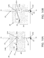
- FIGS. 10A and 10B schematically show the operation of the probe card according to the disclosure, under different operating conditions.
- a probe card according to the disclosure is globally and schematically indicated with 20 .
- the probe card 20 is adapted to connect with an apparatus (not shown in the Figures) for testing electronic devices that are integrated on a semi-conductor wafer.
- the probe card 20 comprises a testing head 21 , which houses a plurality of contact elements 22 , four of said contact elements 22 being shown in FIG. 2A just by way of example.
- the testing head 21 comprises a main body 21 ′ intended to house the contact elements 22 , the main body 21 ′ thus being the support structure of the contact elements 22 .
- the probe card 20 further comprises a support plate 23 , which is preferably a printed circuit board (PCB) that ensures the connection between the probe card 20 and the testing apparatus.
- PCB printed circuit board
- the contact elements 22 comprise a body 22 b , which extends along a longitudinal axis H-H between a first end portion 24 A and a second end portion 24 B, the first end portion 24 A being adapted to abut onto the support plate 23 .
- the probe card 20 further comprises a flexible membrane 25 , which has a first face F 1 , onto which the second end portion 24 B of the contact elements 22 is adapted to abut, and a second face F 2 , opposite the first face F 1 , the second face F 2 being a lower face according to the local reference system of FIG. 2A , namely a face facing a device under test, and the first face F 1 being an upper face according to the local reference system of FIG. 2A , namely a face facing the testing head 21 .
- the testing head 21 is interposed between the flexible membrane 25 and the support place 23 .
- the flexible membrane 25 comprises a first portion or central portion 25 A and a second portion or peripheral portion 25 B, which are intended to contact the testing head 21 and the support plate 23 , respectively.
- the flexible membrane 25 is electrically connected to the support plate 23 by means of the peripheral portion 25 B thereof, said electric connection occurring for instance by means of suitable conductive contact pads 26 of the support plate 23 and of suitable contact pads or conductive portions (not shown) formed on the flexible membrane 25 at its peripheral portion 25 B, as it will be illustrated in the following.
- the contact pads 26 of the support plate 23 are formed on a face F thereof facing the testing head 21 , the face F being a lower face according to the local reference system of FIG. 2A .
- the support plate 23 can comprise suitable openings in order to allow the passage of the flexible membrane 25 therethrough, said flexible membrane 25 being in this case connected to contact pads (not shown) formed on a face opposite to the face F of the support plate 23 , namely on an upper face according to the local reference system of FIG. 2A .
- the flexible membrane 25 can be directly connected to the testing apparatus.
- conductive portions of the flexible membrane 25 are connected to the contact pads 26 of the support plate 23 by means of a pressing contact.
- the flexible membrane 25 and the support plate 23 can be associated by means of a conductive rubber or a weld.
- the support 28 whereon the flexible membrane 25 is arranged, comprises a plurality of guide holes 28 h adapted to slidingly house a plurality of micro contact probes 30 , which are adapted to contact the contact pads 32 of a device under test on a semiconductor wafer 33 , the flexible membrane 25 being interposed between the contact elements 22 and said micro contact probes 30 .
- the probe card 20 further comprises suitable retaining means 29 adapted to keep in place the flexible membrane 25 .
- suitable retaining means 29 adapted to keep in place the flexible membrane 25 .
- the retaining means 29 are in the form of a further support, still indicated with the reference number 29 , the flexible membrane 25 being interposed between the support 28 and said further support 29 .
- the further support 29 comprises a plurality of further guide holes 29 h which adapted to house the contact elements 22 .
- the further support 29 can comprise only one opening for all the contact elements 22 .
- the micro contact probes 30 comprise a body 30 C that extends along the longitudinal axis H-H between a first end portion 30 A and a second end portion 30 B, said second end portion 30 B being adapted to contact the contact pads 32 of the device under test integrated on the semiconductor wafer 33 .
- the flexible membrane 25 is suitably shaped so as to include, preferably in its central portion 25 A, a plurality of strips or fingers 27 (i.e. cutouts in the flexible membrane 25 ).
- the strips 27 protrude and extend in the central portion 25 A of the flexible membrane 25 along an axis H′-H′, which is substantially orthogonal to the axis H-H, between a first end or proximal end 27 A, connected to the flexible membrane 25 , and a second end or distal end 27 B, which protrudes and is not connected to any portion of the flexible membrane 25 .
- the flexible membrane 25 has at least one opening 25 r , preferably formed in the central portion 25 A thereof, in which the strips 27 extend, the distal end 27 B of those strips being thus free, wherein a suitable gap 25 v is defined between adjacent strips and separates them.
- each strip 27 comprises, on the first face F 1 facing the testing head 21 , an upper contact pad 40 , preferably made of a metal material, onto which the second end portion 24 B of the contact elements 22 abuts.
- FIG. 4A which shows a lateral view of a portion of the probe card 20 of FIG. 2B
- the second end portion 24 B of each contact element 22 abuts onto the first face F 1 of the flexible membrane 25 , at the distal end 27 B of a respective strip 27 .
- the first end portion 30 A of each micro contact probe 30 abuts onto the second face F 2 of the flexible membrane 25 , still at said distal end 27 B.
- the second end portion 24 B of the contact elements 22 and the first end portion 30 A of the micro contact probes 30 both abut onto the distal end 27 B of a same respective strip 27 of the flexible membrane 25 , but on opposite sides of such strip 27 , namely onto the first face F 1 and onto the second face F 2 of the flexible membrane 25 , respectively.
- the contact elements 22 abut onto the first face F 1 of the flexible membrane 25 by means of the second end portion 24 B thereof, in particular at the distal end 27 B of a respective strip 27
- the micro contact probes 30 abut onto the second face F 2 of the flexible membrane 25 by means of the first end portion 30 A thereof, in particular at a respective contact element 22 .
- the micro contact probes 30 have a length much lower than the length of the contact probes used in the known solutions, in particular they have a length at least lower than 500 ⁇ m. It should be noted that, in the present description, the term “length” means a dimension of the micro contact probes 30 and of the contact elements 22 measured in a direction parallel to the longitudinal axis H-H.
- micro contact probes 30 of the probe card 20 of the disclosure are adapted to test high-frequency devices, the length thereof being such as to avoid disadvantageous self-inductance phenomena.
- each contact element 22 abuts onto the first face F 1 of a strip 27 of the flexible membrane 25 at the first end portion 30 A of a respective micro contact probe 30 , which in turn abuts onto the second face F 2 of the flexible membrane 25 .
- the number of contact elements 22 in this case corresponds to the number of the micro contact probes 30 , thus resulting in a one-to-one correspondence between said contact elements 22 and said micro contact probes 30 .
- each micro contact probe 30 corresponds to a respective contact element 22 , which abuts onto the flexible membrane 25 but onto the opposite face thereof.
- the contact elements 22 act as damping elements for the micro contact probes 30 , which carry the signals between the probe card 20 and the device under test integrated on the wafer 33 .
- the contact elements 22 are electrically insulated from the micro contact probes 30 , in particular thanks to the flexible membrane 25 interposed therebetween.
- the support 28 and the further support 29 are such as to allow a vertical movement along the longitudinal axis H-H of the strips 27 , in particular of their distal end 27 B.
- a gap 31 is defined between the support 28 and the further support 29 , such as to allow the movement of the distal end 27 B of the strips 27 when the second end portion 30 B of the micro contact probes 30 contacts the contact pads 32 of the device under test.
- the further support 29 comprises a recess 31 ′ that forms the gap 31 between the support 28 and said further support 29 , the strips 27 moving inside this gap 31 .
- the distal ends 27 B of the strips 27 which are flexible, are free to move under the pressure of the micro contact probes 30 when they contact the contact pads 32 of the device under test.
- the recess 31 ′ can be formed by means of a lowering process of the further support 29 .
- the further support 29 can be divided into a first plate-like element, which contacts the flexible membrane 25 and comprises a central opening, and into a second plate-like element, which is on the top of said first plate-like element and comprises the holes for housing the contact elements 22 , the gap 31 being in this case defined by the central opening of the first plate-like element.
- the contact elements 22 act as damping elements (i.e. as shock absorbers), adjusting the contact force exerted on the contact pads 32 of the device under test.
- the contact elements 22 of the testing head 21 have a length generally between 1.5 mm and 10 mm, i.e. a length much greater than that of the micro contact probes 30 which, as previously seen, is lower than 500 ⁇ m, and therefore they have a much greater bending capacity, such as to ensure the aforementioned damping effect.
- the contact elements 22 are made of materials suitable for maximizing the damping effect for the micro contact probes 30 .
- each contact element 22 moves independently of the adjacent ones, so that each micro contact probe 30 moves independently of the adjacent ones when they contact the contact pads 32 of the device under test.
- the contact elements 22 also act as pre-loading elements that keep the flexible membrane 25 , in particular the distal end 27 B of the strips 27 , under pressure against the first end portion 30 A of the micro contact probes 30 , the contact elements 22 thus also ensuring the correct mechanical coupling between the micro contact probes 30 and the flexible membrane 25 .
- the distal end 27 B of the strips 27 of the flexible membrane 25 comprises an opening 34
- the first end portion 30 A of the micro contact probes 30 comprises a protruding portion 35 that engages said opening 34 , allowing in this way a better coupling between the micro contact probes 30 and the flexible membrane 25
- said protruding portion 35 being formed on the top of the first end portion 30 A of the micro contact probes 30 , in particular at an upper edge of the first end portion 30 A, said upper edge being the most faraway one from the proximal portion 27 A of the strips 27 when the micro contact probe 30 is associated with the respective strip 27 .
- the protruding portion 35 engaging with the opening 34 of the strips 27 , also acts as a barrier or containment element for said strips 27 , allowing the formation of a lifted portion L thereof.
- the arrangement of the micro contact probes 30 (which are associated with the distal end 27 B of the strips 27 ) with respect to the proximal end 27 A of the strips 27 determines the presence of the lifted portion L.
- the height h of the lifted portion L which is measured along the axis H-H with respect to the plane where the flexible membrane 25 lies, is suitably calibrated so that, during the overtravel, the distal end 27 B of the strips 27 lifts, thus avoiding excessive traction stresses for the flexible membrane 25 .
- the height h of the lifted portion L is suitably calibrated so that, during the overtravel, the distal end 27 B of the strips 27 lifts by at least 15 ⁇ m.
- each strip 27 comprises, on the second face F 2 , a lower contact pad 39 , which is made of a metallic material and onto which the first end portion 30 A of the micro contact probes 30 abuts, wherein conductive tracks extend from the lower contact pad 39 , as it will be shown below.
- the contact pads 39 and 40 of the flexible membrane 25 are formed in its central portion 25 A, which therefore is a contact area of said flexible membrane 25 , said contact area substantially corresponding to an area of the device under integrated on the wafer 33 comprising the contact pads 32 , the peripheral portion 25 B of the flexible membrane 25 being a portion external to this contact area.
- the lower contact pads 39 and the upper contact pads 40 are further useful for reinforcing the strips 27 of the flexible membrane 25 , in particular they are adapted to damp the abutment of the second end portion 24 B of the contact elements 22 and of the first end portion 30 A of the micro contact probes 30 onto the flexible membrane 25 , substantially acting as a protective structure for said flexible membrane 25 at the strips 27 , in particular at the distal end 27 B thereof.
- the lower contact pads 39 also allow the passage of the signals from the micro contact probes 30 to conductive tracks of the flexible membrane 25 .
- the association between the micro contact probes 30 and the membrane 25 is performed by means of a clip-like attachment.
- the first end portion 30 A of the micro contact probes 30 comprises, on the top thereof, an engagement portion 41 adapted to engage with the opening 34 of the flexible membrane 25 , such an engagement portion 41 comprising a first member 41 a and a second member 41 b separated by a space 41 g , so that when the engagement portion 41 is inserted into the opening 34 of the flexible membrane 25 , the first member 41 a and the second member 41 b are moved one towards the other by the lateral (i.e.
- the conductive layer 40 ′ on the face F 1 facing the contact element 22 is provided with at least one lowered portion 40 ′ l at the opening 34 of the membrane 22 , such a lowered portion 40 ′ l being a housing seat for the second end portion 24 B of the contact element 22 , which abuts onto this housing seat.
- the lowered portion 40 ′ l can be in the form of a through hole and the second end portion 24 B of the contact element 22 abuts directly onto the flexible membrane 25 .
- the guide holes 28 h of the support 28 comprise a recessed portion 281 that forms a shoulder S 1 in each of these guide holes 28 h.
- the support 28 comprises at least one first and one plate-like element, indicated as 28 A and 28 B, respectively, which are overlapped to and integral with each other.
- the first plate-like element 28 A is provided with openings 28 Ah having a diameter greater than corresponding openings 28 Bh of the second plate-like element 28 B, so that when said openings 28 Ah and 28 Bh of the first and second plate-like element are concentrically overlapped, they form the guide holes 28 h of the support 28 , which are provided with the recessed portion 281 previously mentioned.
- the term “diameter” means a maximum transverse dimension.
- the thicknesses of the plate-like elements 28 A and 28 B may vary according to the needs and/or circumstances.
- the thickness of the first plate-like element 28 A may vary from 150 to 200 ⁇ m, preferably 150 ⁇ m
- the thickness of the second plate-like element 28 B may vary from 80 to 150 ⁇ m, preferably 100 ⁇ m.
- the thickness of the further support 29 if any, may vary from 200 to 400 ⁇ m, preferably 250 ⁇ m.
- the plate-like elements 28 A and 28 B can be made of the same material or of different materials. Furthermore, it is possible to provide a support 28 comprising a number of plate-like elements greater than two.
- the first end portion 30 A of the micro contact probes 30 has a diameter D 1 greater than the diameter D 2 of the body 30 C of the micro contact probes 30 , so as to facilitate the association between the distal end 27 B of the strips 27 and such first end portion 30 A.
- the first end portion 30 A of the micro contact probes 30 which has the diameter D 1 greater than the diameter D 2 of the body 30 C, defines a surface S 2 from which a first and a second protruding portions protrude, such protruding portions being indicated as 36 A and 36 B, respectively.
- the first and second protruding portions 36 A and 36 B protrude from the surface S 2 of the first end portion 30 A towards the shoulder S 1 of the guide holes 28 h without abutting thereonto.
- a calibrated gap usually of a few ⁇ m, is present between the first and second protruding portions 36 A and 36 B and the shoulder S 1 .
- the first end portion 30 A of the micro contact probes 30 comprises a beveled portion 37 on the top thereof.
- the beveled portion 37 is formed at an upper edge of the first end portion 30 A, this edge being the closest one to the proximal portion 27 A of the strips 27 when the micro contact probe 30 is associated with the respective strip 27 .
- the beveled portion 37 is formed at the opposite edge with respect to the protruding portion 35 , if any.
- the beveled portion 37 defines, on top of the first end portion 30 A, an inclined surface 37 S onto which the strip 27 lies when the micro contact probes 30 contact the pads 32 of the device under test, namely during the vertical movement or overtravel of the micro contact probes 30 .
- damage to the flexible membrane 25 is avoided during the overtravel, since the flexible membrane 25 is prevented from resting onto a sharp corner.
- the body 30 C of the micro contact probes 30 is a rod-like body suitably tapered.
- the diameter D 2 of the body 30 C of the micro contact probes 30 is variable along the longitudinal axis H-H, so that the body 30 C has a cross-section that is not constant along this longitudinal axis H-H.
- the diameter D 2 is maximum at the first end portion 30 A and is greater than that of the opening 28 Bh of the second plate-like element 28 B, said diameter D 2 decreasing along the longitudinal axis H-H from the first end portion 30 A towards the second end portion 30 B, until it has a constant value.
- the body 30 C of the micro contact probes 30 comprises an enlarged portion 30 D, formed in a portion thereof that is close proximity to the first end portion 30 A, wherein the diameter D 2 has a maximum value at this first end portion 30 A and decreases away from it, the diameter D 2 being constant outside this enlarged portion 30 D, in particular less than the diameter of the opening 28 Bh of the second plate-like element 28 B.
- variable diameter D 2 is obtained by beveling at least one of the four walls of the body 30 C of the micro contact probes 30 , preferably two walls.
- the enlarged portion 30 D, inside which the diameter D 2 is variable can comprise two faces inclined towards the inside of the rod-like body 30 C, these faces being inclined from the lower surface of the first end portion 30 A. These faces possibly have a concavity and are preferably two contiguous faces, the remaining faces being parallel to each other.
- the shape of the body 30 C of the micro contact probes 30 on the one hand avoids them from being stuck in the guide holes 28 h , and on the other hand it reduces the clearance between them and the walls of said guide holes 28 h , in particular the walls of the openings 28 Bh of the second plate-like element 28 B.
- the retention of the micro contact probes 30 within the guide holes 28 h is obtained thanks to the abutment of the inclined faces of the enlarged portion 30 D against the edges of the shoulder S 1 .
- the retention is obtained thanks to the abutment of the first and second protruding portions 36 A and 36 B against the shoulder S 1 of the guide holes 28 h.
- the shape of the body 30 C allows the micro contact probes 30 to be repositioned, under the load of the pre-loading contact elements 22 , in the same operating position after they have contacted the contact pads 32 of the device under test.
- FIGS. 4A, 4B, 5A and 5B is provided only by way of non-limiting example of the disclosure, since the micro contact probes 30 can be of any suitable shape.
- the flexible membrane 25 comprises suitable conductive tracks 38 for carrying and routing signals between the device under test and the support plate 23 , as it was previously mentioned.
- the conductive tracks 38 extend from the distal end 27 B of the strips 27 , in particular from the strip point at which the first end portion 30 A of the micro contact probes 30 abuts.
- the flexible membrane 25 provides for the routing of the signals towards the PCB by means of the conductive tracks 38 , and therefore it also performs the function generally performed by the space transformers of the known probe cards.
- the probe card 20 may further comprise an additional board having the function of space transformer, so that the routing of the signals can be performed both by the conductive tracks 38 of the flexible membrane 25 and by this space transformer.
- the contact elements 22 are not adapted to carry signals but are included only as damping elements of the probe card 20 , so as to overcome the problem of the rigidity of the micro contact probes 30 and to avoid the breakage thereof during the contact with the contact pads 32 of the device under test.
- a group 22 ′ of the contact elements 22 is also adapted to carry signals between the device under test and the testing apparatus.
- Each contact element of this group 22 ′ is thus electrically connected to a corresponding micro contact probe 30 by means of connection conductive tracks 38 ′ in the flexible membrane 25 , said connection conductive tracks 38 ′ extending between the first face F 1 and the second face F 2 of the flexible membrane 25 .
- the connection conductive tracks 38 ′ are adapted to connect the opposite faces F 1 and F 2 of the flexible membrane 25 to each other, these tracks being formed for instance by filling through-holes or through-paths made in the flexible membrane 25 with a conductive material.
- the contact elements of the group 22 ′ thus perform a dual function, namely on the one hand they act as damping elements of the probe card 20 , in particular of the micro contact probes 30 , and on the other hand they carry signals towards the support plate 23 .
- the contact elements not included in the group 22 ′ are electrically insulated from the micro contact probes 30 (and also from the other contact elements) and only act as damping elements.
- the contact elements of the group 22 ′ are adapted to carry power signals and/or ground signals and/or low-frequency signals between the device under test and said support plate 23 .
- the support plate 23 comprises further conductive contact pads (not shown in the Figures) at the first end portion 24 A′ of the contact elements of the group 22 ′, onto which these end portions abut for actually carrying the signals towards the testing apparatus.
- connection conductive tracks 38 ′ can connect the lower contact pad 39 of the face F 1 and the upper contact pad 40 of the face F 2 , or it is possible to make just one conductive pad that passes through the flexible membrane 25 and emerges on said faces F 1 and F 2 .
- the conductive tracks 38 extend from the central portion 25 A of the flexible membrane 25 along the strips 27 up to the peripheral portion 25 B, so as to connect to the support plate 23 .
- the conductive tracks 38 are electrically connected, for instance by means of a pressing contact or a weld, to the contact pads 26 of the support plate 23 .
- the conductive tracks 38 extend along the second face F 2 of the flexible membrane 25 from the respective micro contact probe 30 , in particular from the respective lower contact pad 39 .
- the conductive tracks 38 can also extend on the first face F 1 of the flexible membrane 25 , if required by the configuration.
- the conductive tracks 38 can also extend within the flexible membrane 25 (namely they can be embedded therein).
- the conductive tracks 38 in the flexible membrane 25 are made on different levels starting from the second face F 2 .
- the number of levels of the flexible membrane 25 where the conductive tracks 38 are made may vary according to the needs and/or circumstances, in particular according to the number of signals to be carried and thus according to the complexity of the routing pattern of the flexible membrane 25 .
- a configuration can be provided wherein a first level comprises tracks adapted to carry the power signal and a second level comprises tracks adapted to carry the ground signal.
- the micro contact probes 30 which are adapted to contact the contact pads 32 of the device under test integrated on the semiconductor wafer 33 , are made of a conductive material or of a suitable alloy.
- the flexible membrane 25 is made of dielectric materials, preferably polyamide, capable of providing the desired flexibility and the desired electric insulation, whereas the conductive tracks 38 are made of a conductive metallic material, preferably copper.
- the support plate 23 is similar the known PCBs, with the difference that its contact pads 26 are preferably made on a peripheral portion thereof, so that these contact pads 26 can electrically contact the conductive tracks 38 (or possible pads of the membrane) at the peripheral portion 25 B of the flexible membrane 25 .
- the support 28 and the further support 29 are preferably made of a ceramic material.
- the length of the strips 27 may vary according to the needs and/or circumstances.
- the length of the strips 27 can be very small, slightly greater than a maximum dimension of the lower contact pads 39 , for instance in order to reduce the path of some ground signals.
- the flexible membrane 25 comprises strips whose length is slightly greater than the lower contact pads 39 , and also strips having greater extension.
- the testing head 21 of the probe card 20 comprises further contact elements 22 bis adapted to carry power signals and/or ground signals and/or low-frequency signals between the device under test and the support plate 23 , i.e. signals that can be carried also by longer probes.
- the support 28 comprises in this case further guide holes 28 h ′ for the passage of the further contact elements 22 bis .
- the further support 29 comprises a plurality of second guide holes 29 h ′, which are concentric to the further guide holes 28 h ′, for the passage of the further contact elements 22 bis.
- the further guide holes 28 h ′ are formed in the support 28 in an area thereof that substantially corresponds to the opening 25 r of the flexible membrane 25 , so as not to further pierce the flexible membrane 25 .
- the flexible membrane 25 can be further shaped or cutout so as to allow the passage of the further contact elements 22 bis in any portion.
- the contact elements 22 and the further contact elements 22 bis are designed so that these further contact elements 22 bis and the micro contact probes 30 exert substantially identical forces onto the contact pads 32 of the device under test during the overtravel, as well as comparable scrubs.
- FIGS. 10A and 10B the operation of the probe card 20 according to the disclosure is shown, under different operating conditions.
- the strips 27 of the flexible membrane 25 are lifted and move along the longitudinal axis H-H, while the contact elements 22 always ensure the correct pressure of the micro contact probes 30 onto the contact pads 32 of the device under test, as well as the correct pressure of the flexible membrane 25 onto the first end portion 30 A of said micro contact probes 30 .
- the lifted portion L of the strips 27 is such as to avoid unfavorable traction stresses.
- the pressure exerted by the contact elements 22 onto the micro contact probes 30 is suitably calibrated so that, on the one hand the flexible membrane 25 is always pushed against the first end portion 30 A of the micro contact probes 30 , and that on the other hand a correct mechanical and electric contact of the micro contact probes 30 with the device under test is always ensured, i.e. it is calibrated taking into account both the pre-loading pressure and the working pressure.
- the main body 21 ′ of the testing head 21 comprises at least one guide provided with a plurality of guide holes within which the contact elements 22 are slidingly housed.
- the disclosure provides a probe card provided with micro contact probes adapted to contact a device to be tested, each of those micro contact probes having an end portion abutting onto an end of a respective strip of a plurality of strips formed in a flexible membrane of the probe card, wherein contact elements of a testing head of the probe card also have an end portion abutting onto such end of the strips but onto an opposite face of the flexile membrane, in this way acting as damping support elements for the corresponding micro contact probes, the end portion of those strips moving during the contact of the micro contact probes with the device to be tested.
- the probe card is particularly performing in radiofrequency applications, thanks to the reduced dimensions of the micro contact probes comprised therein, having a length much lower than that of the contact elements and in particular lower than 500 ⁇ m.
- the presence of the contact elements of the testing head interposed between the flexible membrane and the PCB, which act as damping elements for each micro contact probe (namely they are adapted to damp the contact between the micro contact probe and the contact pads of a device under test), allows overcoming the problem of the rigidity of said micro contact probes having a reduced length, drastically reducing the possibility of breakage of the microprobes themselves, at the same time ensuring a proper reduction in the pressure they exert, avoiding any breakages of the contact pads of the devices under test onto which the micro contact probes abut.
- the contact elements of the testing head thanks to their length greater than the one of the respective micro contact probes, have a much greater bending capacity.
- the probe card of the disclosure on the one hand allows testing high-frequency electronic devices, and on the other hand allows avoiding the breakage of its micro contact probes and/or of the contact pads of the device under test, thus solving the technical problem of the disclosure.
- the micro contact probes of the probe card of the disclosure have a very long working life, said micro contact probes being in any case easily replaceable.
- each of those contact elements providing a support for a corresponding micro contact probe independently of the other contact elements and of the other micro contact probes, therefore compensating for any possible lack of uniformity in the probe card, in terms of levels, heights and force exerted onto the pads.
- the probe card of the disclosure works correctly even in case of planarity problems of its components or of the wafer and of the devices under test comprised therein.
- the contact elements also act as pre-loading elements for the micro contact probes, ensuring the micro contact probes to always be associated with the respective flexible strip of the membrane, which also performs the desired routing of the signals within the probe card.
- the flexible membrane, the micro contact probes and the contact elements are structurally independent from each other, thereby ensuring a prober operation of the probe card.
- the contact elements are not fixedly fastened (i.e. soldered) to the flexible membrane and simply abut onto this flexible membrane, thus avoiding possible undesirable stresses.
- the hybrid configuration in which further contact elements are adapted to carry specific signals, greatly simplifies the signal routing by the flexible membrane, especially in the case of several signals to be carried by the probe card.
- the further contact elements it is possible to carry power signals and/or ground signals, namely signals that do not require short contact probes, whereas the high-frequency signals, which require short probes to avoid self-inductance problems, are carried by the micro contact probes associated with the flexible membrane.
Landscapes
- Physics & Mathematics (AREA)
- General Physics & Mathematics (AREA)
- Engineering & Computer Science (AREA)
- Geometry (AREA)
- Computer Hardware Design (AREA)
- Microelectronics & Electronic Packaging (AREA)
- General Engineering & Computer Science (AREA)
- Measuring Leads Or Probes (AREA)
- Testing Or Measuring Of Semiconductors Or The Like (AREA)
- Testing Of Individual Semiconductor Devices (AREA)
- Inorganic Insulating Materials (AREA)
- Polyesters Or Polycarbonates (AREA)
Abstract
Description
Claims (25)
Applications Claiming Priority (3)
| Application Number | Priority Date | Filing Date | Title |
|---|---|---|---|
| IT102017000017061A IT201700017061A1 (en) | 2017-02-15 | 2017-02-15 | Improved measurement card for high frequency applications |
| IT102017000017061 | 2017-02-15 | ||
| PCT/EP2018/053593 WO2018149838A1 (en) | 2017-02-15 | 2018-02-13 | Improved probe card for high-frequency applications |
Related Parent Applications (1)
| Application Number | Title | Priority Date | Filing Date |
|---|---|---|---|
| PCT/EP2018/053593 Continuation-In-Part WO2018149838A1 (en) | 2017-02-15 | 2018-02-13 | Improved probe card for high-frequency applications |
Publications (2)
| Publication Number | Publication Date |
|---|---|
| US20190361051A1 US20190361051A1 (en) | 2019-11-28 |
| US11029336B2 true US11029336B2 (en) | 2021-06-08 |
Family
ID=59297241
Family Applications (1)
| Application Number | Title | Priority Date | Filing Date |
|---|---|---|---|
| US16/537,770 Active 2038-02-21 US11029336B2 (en) | 2017-02-15 | 2019-08-12 | Probe card for high-frequency applications |
Country Status (10)
| Country | Link |
|---|---|
| US (1) | US11029336B2 (en) |
| EP (1) | EP3583430B1 (en) |
| JP (1) | JP7104054B2 (en) |
| KR (1) | KR102515947B1 (en) |
| CN (1) | CN110312940B (en) |
| IT (1) | IT201700017061A1 (en) |
| PH (1) | PH12019501890A1 (en) |
| SG (1) | SG11201907123PA (en) |
| TW (1) | TWI717585B (en) |
| WO (1) | WO2018149838A1 (en) |
Cited By (2)
| Publication number | Priority date | Publication date | Assignee | Title |
|---|---|---|---|---|
| US12169208B2 (en) | 2021-11-30 | 2024-12-17 | Innovatum Instruments Inc. | Probe tip X-Y location identification using a charged particle beam |
| US12306241B2 (en) | 2022-02-14 | 2025-05-20 | Innovatum Instruments Inc. | Automated probe landing |
Families Citing this family (29)
| Publication number | Priority date | Publication date | Assignee | Title |
|---|---|---|---|---|
| JP7249281B2 (en) | 2016-12-23 | 2023-03-30 | クアンタム ダイヤモンド テクノロジーズ インク. | Method and apparatus for magnetic multi-bead assay |
| IT201700017037A1 (en) * | 2017-02-15 | 2018-08-15 | Technoprobe Spa | Measurement board for high frequency applications |
| CN108241078B (en) * | 2017-05-18 | 2020-06-02 | 苏州韬盛电子科技有限公司 | Vertical probe card |
| ES2932362T3 (en) * | 2017-07-31 | 2023-01-18 | Quantum Diamond Tech Inc | Sensor system comprising a sample cartridge including a flexible membrane to support a sample |
| IT201800021253A1 (en) * | 2018-12-27 | 2020-06-27 | Technoprobe Spa | Vertical probe measuring head having an improved contact with a device to be tested |
| DE102019107138A1 (en) * | 2019-03-20 | 2020-09-24 | OSRAM Opto Semiconductors Gesellschaft mit beschränkter Haftung | METHOD AND DEVICE FOR ELECTRICAL CONTACTING OF COMPONENTS IN A SEMICONDUCTOR WAFER |
| US11346860B2 (en) * | 2019-08-15 | 2022-05-31 | Mpi Corporation | Probe head for high frequency signal test and medium or low frequency signal test at the same time |
| IT201900024964A1 (en) * | 2019-12-20 | 2021-06-20 | Technoprobe Spa | Measuring head for low pitch applications |
| CN111579833B (en) * | 2020-05-18 | 2022-12-23 | 武汉精毅通电子技术有限公司 | Probe and connector suitable for high-current high-speed signal test |
| JP7250112B2 (en) * | 2020-05-19 | 2023-03-31 | グーグル エルエルシー | Using crowdsourcing to combat disinformation |
| KR102307942B1 (en) * | 2020-07-13 | 2021-10-01 | 양진석 | Apparatus for testing a semiconductor device |
| CN114545042B (en) * | 2020-11-24 | 2025-07-18 | 台湾中华精测科技股份有限公司 | Probe card device and self-aligned probe |
| IT202000028370A1 (en) | 2020-11-25 | 2022-05-25 | Technoprobe Spa | FLEXIBLE MEMBRANE SUITABLE FOR THE TRANSPORT OF HIGH FREQUENCY (RF) POWER SIGNALS AND CORRESPONDING MEASUREMENT BOARD FOR HIGH FREQUENCY (RF) POWER TESTING OF ELECTRONIC DEVICES |
| CN112362922A (en) * | 2020-11-25 | 2021-02-12 | 广州国显科技有限公司 | Lighting test fixture, fixing piece and lighting test device |
| TWI758991B (en) * | 2020-12-04 | 2022-03-21 | 致茂電子股份有限公司 | Probe device |
| TWI784439B (en) * | 2021-03-12 | 2022-11-21 | 冠銓科技實業股份有限公司 | Test needle seat structure for high frequency measurement |
| KR102577539B1 (en) * | 2021-04-09 | 2023-09-12 | (주)포인트엔지니어링 | The Electro-conductive Contact Pin and Manufacturing Method thereof |
| CN113466504B (en) * | 2021-09-03 | 2021-11-19 | 绅克半导体科技(苏州)有限公司 | Test probe, test probe module and test device |
| JP2023064802A (en) * | 2021-10-27 | 2023-05-12 | 株式会社ヨコオ | Flexible substrates and inspection jig |
| CN114200280B (en) * | 2021-11-29 | 2022-11-15 | 强一半导体(苏州)有限公司 | Film probe card and probe head thereof |
| CN116359569A (en) * | 2021-12-27 | 2023-06-30 | 财团法人工业技术研究院 | Probe card |
| CN115616260B (en) * | 2022-09-26 | 2024-02-23 | 上海泽丰半导体科技有限公司 | Thin film probe card assembly |
| TWI865981B (en) * | 2022-12-06 | 2024-12-11 | 旺矽科技股份有限公司 | Probe card device |
| JP2024147205A (en) * | 2023-04-03 | 2024-10-16 | 株式会社日本マイクロニクス | Method for manufacturing probe and electrical connection device |
| CN119199206A (en) * | 2023-06-27 | 2024-12-27 | 迪科特测试科技(苏州)有限公司 | Probe card structure comprising probe groups with different lengths |
| CN119199205A (en) * | 2023-06-27 | 2024-12-27 | 迪科特测试科技(苏州)有限公司 | Probe card structure |
| TWI863494B (en) * | 2023-08-09 | 2024-11-21 | 思達科技股份有限公司 | Probe card structure |
| JP2025074065A (en) * | 2023-10-27 | 2025-05-13 | 旺▲夕▼科技股▲分▼有限公司 | Vertical probe, probe head, and method for manufacturing vertical probe |
| TW202603385A (en) * | 2024-04-10 | 2026-01-16 | 義大利商探針科技公司 | Measuring system for performing high-voltage tests and related apparatus |
Citations (9)
| Publication number | Priority date | Publication date | Assignee | Title |
|---|---|---|---|---|
| JPS596500A (en) | 1982-07-02 | 1984-01-13 | Sumitomo Metal Ind Ltd | Leakage detection method of liquid transferring pipeline |
| US5252916A (en) * | 1992-01-27 | 1993-10-12 | Everett Charles Technologies, Inc. | Pneumatic test fixture with springless test probes |
| US5389885A (en) * | 1992-01-27 | 1995-02-14 | Everett Charles Technologies, Inc. | Expandable diaphragm test modules and connectors |
| US5633598A (en) * | 1993-06-23 | 1997-05-27 | Everett Charles Technologies, Inc. | Translator fixture with module for expanding test points |
| US20040036493A1 (en) | 2002-05-08 | 2004-02-26 | Miller Charles A. | High performance probe system |
| US20040046579A1 (en) | 2002-05-08 | 2004-03-11 | Formfactor, Inc. | High performance probe system |
| US20040070413A1 (en) | 2002-10-02 | 2004-04-15 | Susumu Kasukabe | Probe sheet, probe card, semiconductor test equipment and semiconductor device fabrication method |
| JP3596500B2 (en) | 2001-09-10 | 2004-12-02 | セイコーエプソン株式会社 | Method for manufacturing semiconductor inspection device, semiconductor inspection device, and method for inspecting semiconductor device |
| US20080061808A1 (en) | 2006-09-12 | 2008-03-13 | Sammy Mok | Compliance partitioning in testing of integrated circuits |
Family Cites Families (23)
| Publication number | Priority date | Publication date | Assignee | Title |
|---|---|---|---|---|
| JP3194669B2 (en) * | 1993-05-19 | 2001-07-30 | 東京エレクトロン株式会社 | Inspection device and connection method in inspection device |
| US5583445A (en) * | 1994-02-04 | 1996-12-10 | Hughes Aircraft Company | Opto-electronic membrane probe |
| CN1208624C (en) * | 1996-05-17 | 2005-06-29 | 福姆法克特公司 | Method for making interconnection elements |
| ATE346310T1 (en) * | 2001-01-31 | 2006-12-15 | Wentworth Lab Inc | NICKEL ALLOY PROBE CARD FRAME LAMINATE |
| JP2004144742A (en) * | 2002-10-02 | 2004-05-20 | Renesas Technology Corp | Probe sheet, probe card, semiconductor inspection apparatus, and method for manufacturing semiconductor device |
| KR20050083184A (en) * | 2003-03-17 | 2005-08-26 | 프롬써어티 주식회사 | Probe card for testing semiconductor |
| US7383518B1 (en) * | 2004-11-01 | 2008-06-03 | Synopsys, Inc. | Method and apparatus for performance metric compatible control of data transmission signals |
| KR100661254B1 (en) * | 2005-01-06 | 2006-12-28 | (주) 미코티엔 | Probe Card for Semiconductor Inspection |
| US7368928B2 (en) * | 2006-08-29 | 2008-05-06 | Mjc Probe Incorporation | Vertical type high frequency probe card |
| KR100882512B1 (en) * | 2007-04-25 | 2009-02-10 | 윌테크놀러지(주) | Probe card |
| KR100799128B1 (en) * | 2007-08-14 | 2008-01-29 | 주식회사 파이컴 | Electrical inspection device |
| JP5219633B2 (en) * | 2008-06-05 | 2013-06-26 | 東京特殊電線株式会社 | High frequency measurement probe |
| CN201464507U (en) * | 2009-07-31 | 2010-05-12 | 中芯国际集成电路制造(上海)有限公司 | Probe card and metal probe |
| KR101674135B1 (en) * | 2010-01-13 | 2016-11-09 | (주)엠투엔 | Probe card |
| KR20110139827A (en) * | 2010-06-24 | 2011-12-30 | (주) 미코티엔 | Probe card and its manufacturing method |
| KR101805816B1 (en) * | 2011-01-04 | 2017-12-07 | (주)엠투엔 | Probe card |
| US8884640B2 (en) * | 2011-04-28 | 2014-11-11 | Mpi Corporation | Integrated high-speed probe system |
| TWI542889B (en) * | 2011-06-03 | 2016-07-21 | Hioki Electric Works | A detection unit, a circuit board detection device, and a detection unit manufacturing method |
| US9891273B2 (en) * | 2011-06-29 | 2018-02-13 | Taiwan Semiconductor Manufacturing Company, Ltd. | Test structures and testing methods for semiconductor devices |
| US10006938B2 (en) * | 2012-01-04 | 2018-06-26 | Formfactor, Inc. | Probes with programmable motion |
| ITMI20120996A1 (en) * | 2012-06-08 | 2013-12-09 | Technoprobe Spa | MEASUREMENT CARD FOR A TEST DEVICE OF ELECTRONIC DEVICES |
| KR101704188B1 (en) * | 2015-04-23 | 2017-02-22 | 김일 | Probe Card with Wire Probes |
| WO2016177850A1 (en) * | 2015-05-07 | 2016-11-10 | Technoprobe S.P.A. | Testing head having vertical probes, in particular for reduced pitch applications |
-
2017
- 2017-02-15 IT IT102017000017061A patent/IT201700017061A1/en unknown
-
2018
- 2018-02-13 EP EP18707644.3A patent/EP3583430B1/en active Active
- 2018-02-13 WO PCT/EP2018/053593 patent/WO2018149838A1/en not_active Ceased
- 2018-02-13 SG SG11201907123PA patent/SG11201907123PA/en unknown
- 2018-02-13 KR KR1020197026817A patent/KR102515947B1/en active Active
- 2018-02-13 CN CN201880011989.2A patent/CN110312940B/en active Active
- 2018-02-13 JP JP2019543214A patent/JP7104054B2/en not_active Expired - Fee Related
- 2018-02-14 TW TW107105488A patent/TWI717585B/en active
-
2019
- 2019-08-12 US US16/537,770 patent/US11029336B2/en active Active
- 2019-08-14 PH PH12019501890A patent/PH12019501890A1/en unknown
Patent Citations (9)
| Publication number | Priority date | Publication date | Assignee | Title |
|---|---|---|---|---|
| JPS596500A (en) | 1982-07-02 | 1984-01-13 | Sumitomo Metal Ind Ltd | Leakage detection method of liquid transferring pipeline |
| US5252916A (en) * | 1992-01-27 | 1993-10-12 | Everett Charles Technologies, Inc. | Pneumatic test fixture with springless test probes |
| US5389885A (en) * | 1992-01-27 | 1995-02-14 | Everett Charles Technologies, Inc. | Expandable diaphragm test modules and connectors |
| US5633598A (en) * | 1993-06-23 | 1997-05-27 | Everett Charles Technologies, Inc. | Translator fixture with module for expanding test points |
| JP3596500B2 (en) | 2001-09-10 | 2004-12-02 | セイコーエプソン株式会社 | Method for manufacturing semiconductor inspection device, semiconductor inspection device, and method for inspecting semiconductor device |
| US20040036493A1 (en) | 2002-05-08 | 2004-02-26 | Miller Charles A. | High performance probe system |
| US20040046579A1 (en) | 2002-05-08 | 2004-03-11 | Formfactor, Inc. | High performance probe system |
| US20040070413A1 (en) | 2002-10-02 | 2004-04-15 | Susumu Kasukabe | Probe sheet, probe card, semiconductor test equipment and semiconductor device fabrication method |
| US20080061808A1 (en) | 2006-09-12 | 2008-03-13 | Sammy Mok | Compliance partitioning in testing of integrated circuits |
Cited By (2)
| Publication number | Priority date | Publication date | Assignee | Title |
|---|---|---|---|---|
| US12169208B2 (en) | 2021-11-30 | 2024-12-17 | Innovatum Instruments Inc. | Probe tip X-Y location identification using a charged particle beam |
| US12306241B2 (en) | 2022-02-14 | 2025-05-20 | Innovatum Instruments Inc. | Automated probe landing |
Also Published As
| Publication number | Publication date |
|---|---|
| KR20190117015A (en) | 2019-10-15 |
| US20190361051A1 (en) | 2019-11-28 |
| EP3583430B1 (en) | 2021-01-20 |
| EP3583430A1 (en) | 2019-12-25 |
| KR102515947B1 (en) | 2023-03-29 |
| JP2020507769A (en) | 2020-03-12 |
| PH12019501890A1 (en) | 2019-10-21 |
| TW201840987A (en) | 2018-11-16 |
| WO2018149838A1 (en) | 2018-08-23 |
| CN110312940B (en) | 2021-11-12 |
| JP7104054B2 (en) | 2022-07-20 |
| IT201700017061A1 (en) | 2018-08-15 |
| TWI717585B (en) | 2021-02-01 |
| CN110312940A (en) | 2019-10-08 |
| SG11201907123PA (en) | 2019-09-27 |
Similar Documents
| Publication | Publication Date | Title |
|---|---|---|
| US11029336B2 (en) | Probe card for high-frequency applications | |
| US10578646B2 (en) | Testing head comprising vertical probes with internal openings | |
| US11415600B2 (en) | Probe card for high frequency applications | |
| US11402428B2 (en) | High-performance probe card in high-frequency | |
| US11112431B2 (en) | Probe card for high-frequency applications | |
| JP5289771B2 (en) | Probe card | |
| TWI865696B (en) | A testing head with an improved contact between contact probes and guide holes | |
| KR20190039122A (en) | Contact probes and corresponding test heads of devices for testing electronic devices | |
| US20200200795A1 (en) | Interface element for a testing apparatus of electronic devices and corresponding manufacturing method | |
| KR102790096B1 (en) | Needle unit for electrical property inspection apparatus | |
| TW202409588A (en) | Improved measurement system for the testing of high-frequency devices | |
| KR20240081020A (en) | probe card for vertical type with scrub length control | |
| JPH06281671A (en) | Probe card | |
| JP2010103238A (en) | Device for manufacturing semiconductor |
Legal Events
| Date | Code | Title | Description |
|---|---|---|---|
| FEPP | Fee payment procedure |
Free format text: ENTITY STATUS SET TO UNDISCOUNTED (ORIGINAL EVENT CODE: BIG.); ENTITY STATUS OF PATENT OWNER: LARGE ENTITY |
|
| STPP | Information on status: patent application and granting procedure in general |
Free format text: DOCKETED NEW CASE - READY FOR EXAMINATION |
|
| AS | Assignment |
Owner name: TECHNOPROBE S.P.A., ITALY Free format text: ASSIGNMENT OF ASSIGNORS INTEREST;ASSIGNORS:VETTORI, RICCARDO;FELICI, STEFANO;REEL/FRAME:050564/0764 Effective date: 20190918 |
|
| STPP | Information on status: patent application and granting procedure in general |
Free format text: NOTICE OF ALLOWANCE MAILED -- APPLICATION RECEIVED IN OFFICE OF PUBLICATIONS |
|
| STPP | Information on status: patent application and granting procedure in general |
Free format text: NOTICE OF ALLOWANCE MAILED -- APPLICATION RECEIVED IN OFFICE OF PUBLICATIONS |
|
| STPP | Information on status: patent application and granting procedure in general |
Free format text: DOCKETED NEW CASE - READY FOR EXAMINATION |
|
| STPP | Information on status: patent application and granting procedure in general |
Free format text: NOTICE OF ALLOWANCE MAILED -- APPLICATION RECEIVED IN OFFICE OF PUBLICATIONS |
|
| STPP | Information on status: patent application and granting procedure in general |
Free format text: PUBLICATIONS -- ISSUE FEE PAYMENT RECEIVED |
|
| STPP | Information on status: patent application and granting procedure in general |
Free format text: PUBLICATIONS -- ISSUE FEE PAYMENT VERIFIED |
|
| STCF | Information on status: patent grant |
Free format text: PATENTED CASE |
|
| MAFP | Maintenance fee payment |
Free format text: PAYMENT OF MAINTENANCE FEE, 4TH YEAR, LARGE ENTITY (ORIGINAL EVENT CODE: M1551); ENTITY STATUS OF PATENT OWNER: LARGE ENTITY Year of fee payment: 4 |