US11029222B2 - Pressure sensor having conductive material extending between non-porous and porous regions and pressure sensing device comprising same - Google Patents
Pressure sensor having conductive material extending between non-porous and porous regions and pressure sensing device comprising same Download PDFInfo
- Publication number
- US11029222B2 US11029222B2 US16/313,110 US201616313110A US11029222B2 US 11029222 B2 US11029222 B2 US 11029222B2 US 201616313110 A US201616313110 A US 201616313110A US 11029222 B2 US11029222 B2 US 11029222B2
- Authority
- US
- United States
- Prior art keywords
- electrode layer
- pressure sensor
- conductive
- foam
- region
- Prior art date
- Legal status (The legal status is an assumption and is not a legal conclusion. Google has not performed a legal analysis and makes no representation as to the accuracy of the status listed.)
- Active
Links
Images


Classifications
-
- G—PHYSICS
- G01—MEASURING; TESTING
- G01L—MEASURING FORCE, STRESS, TORQUE, WORK, MECHANICAL POWER, MECHANICAL EFFICIENCY, OR FLUID PRESSURE
- G01L1/00—Measuring force or stress, in general
- G01L1/20—Measuring force or stress, in general by measuring variations in ohmic resistance of solid materials or of electrically-conductive fluids; by making use of electrokinetic cells, i.e. liquid-containing cells wherein an electrical potential is produced or varied upon the application of stress
-
- G—PHYSICS
- G01—MEASURING; TESTING
- G01L—MEASURING FORCE, STRESS, TORQUE, WORK, MECHANICAL POWER, MECHANICAL EFFICIENCY, OR FLUID PRESSURE
- G01L1/00—Measuring force or stress, in general
- G01L1/18—Measuring force or stress, in general using properties of piezo-resistive materials, i.e. materials of which the ohmic resistance varies according to changes in magnitude or direction of force applied to the material
-
- G—PHYSICS
- G01—MEASURING; TESTING
- G01L—MEASURING FORCE, STRESS, TORQUE, WORK, MECHANICAL POWER, MECHANICAL EFFICIENCY, OR FLUID PRESSURE
- G01L1/00—Measuring force or stress, in general
- G01L1/20—Measuring force or stress, in general by measuring variations in ohmic resistance of solid materials or of electrically-conductive fluids; by making use of electrokinetic cells, i.e. liquid-containing cells wherein an electrical potential is produced or varied upon the application of stress
- G01L1/22—Measuring force or stress, in general by measuring variations in ohmic resistance of solid materials or of electrically-conductive fluids; by making use of electrokinetic cells, i.e. liquid-containing cells wherein an electrical potential is produced or varied upon the application of stress using resistance strain gauges
- G01L1/2287—Measuring force or stress, in general by measuring variations in ohmic resistance of solid materials or of electrically-conductive fluids; by making use of electrokinetic cells, i.e. liquid-containing cells wherein an electrical potential is produced or varied upon the application of stress using resistance strain gauges constructional details of the strain gauges
-
- H—ELECTRICITY
- H01—ELECTRIC ELEMENTS
- H01B—CABLES; CONDUCTORS; INSULATORS; SELECTION OF MATERIALS FOR THEIR CONDUCTIVE, INSULATING OR DIELECTRIC PROPERTIES
- H01B1/00—Conductors or conductive bodies characterised by the conductive materials; Selection of materials as conductors
- H01B1/20—Conductive material dispersed in non-conductive organic material
- H01B1/22—Conductive material dispersed in non-conductive organic material the conductive material comprising metals or alloys
-
- H—ELECTRICITY
- H01—ELECTRIC ELEMENTS
- H01B—CABLES; CONDUCTORS; INSULATORS; SELECTION OF MATERIALS FOR THEIR CONDUCTIVE, INSULATING OR DIELECTRIC PROPERTIES
- H01B1/00—Conductors or conductive bodies characterised by the conductive materials; Selection of materials as conductors
- H01B1/20—Conductive material dispersed in non-conductive organic material
- H01B1/24—Conductive material dispersed in non-conductive organic material the conductive material comprising carbon-silicon compounds, carbon or silicon
Definitions
- the present invention relates to a pressure sensor, and more specifically, to a sensor and device for sensing a pressure.
- a device for sensing a pressure in various application fields using a pressure from a body, as well as a safety device for home use, is required.
- a pressure sensing device includes a lower electrode, an intermediate layer disposed on the lower electrode, and an upper electrode disposed on the intermediate layer.
- the intermediate layer has elasticity and may include a conductive filler.
- the performance of the pressure sensing device may be influenced by the elastic restoring force and conduction performance of the intermediate layer.
- the intermediate layer may be manufactured through a process of immersing an elastic foam in a conductive solution and cleaning and drying the foam.
- the conductive filler attached to a surface of the elastic foam may be detached, and the detached conductive filler may become a surrounding pollution source and may cause sensitivity degradation of the pressure sensing device.
- the elastic restoring force of the intermediate layer may be degraded.
- the present invention is directed to providing a pressure sensing device for sensing a pressure according to an applied weight.
- One aspect of the present invention provides a pressure sensor which includes a first electrode layer, a second electrode layer, and an intermediate layer disposed between the first electrode layer and the second electrode layer, wherein the intermediate layer includes a foam in which a porous region is dispersed in a non-porous region and a conductive material dispersed in the foam and having a conductivity rate that is higher than that of the foam.
- At least a part of the conductive material may be dispersed in the non-porous region.
- the at least a part of the conductive material may pass through an interface between the non-porous region and the porous region.
- the at least a part of the conductive material may be dispersed in the porous region.
- a ratio of the porous region in the foam to the foam may be in a range of 5 to 90%.
- a resistance of the intermediate layer may be changed according to change in at least one of a thickness and a volume of the intermediate layer.
- the foam may be selected from the group consisting of polyurethane, polyolefin, rubber, silicone, and elastomer.
- the conductive material may be selected from the group consisting of Au, Ag, Cu, Ni, carbon nano tube (CNT), carbon black, graphene, a ceramic material, and a conductive polymer.
- Each of the first electrode layer and the second electrode layer may be made of a conductive fiber.
- a pressure sensor which includes a first electrode layer, a second electrode layer disposed to be spaced apart from the first electrode layer on a horizontal surface, and an intermediate layer disposed on or under the first electrode layer and the second electrode layer, wherein the intermediate layer includes a foam in which a porous region is disposed in a non-porous region and includes a conductive material dispersed in the foam and having a conductivity rate that is higher than that of the foam.
- Still another aspect of the present invention provides a pressure sensing device which includes a pressure sensor, a signal processing unit connected with the pressure sensor and configured to process an electric signal generated by the pressure sensor, and a control unit connected with the signal processing unit and configured to generate a control signal based on a signal processed by the signal processing unit, wherein the pressure sensor includes a first electrode layer, a second electrode layer, and an intermediate layer disposed between the first electrode layer and the second electrode layer, wherein the intermediate layer includes a foam in which a porous region is dispersed in a non-porous region and a conductive material dispersed in the foam and having a conductivity rate that is higher than that of the foam.
- a pressure sensing device can precisely detect a pressure caused according to an applied weight and can precisely detect pressure distribution.
- detachment of a conductive filler is minimized, and thus a pressure sensing device with high elastic restoring force and high durability can be obtained. Further, according to the embodiment of the present invention, a manufacturing process can be simplified.
- FIG. 1 is a perspective view of a pressure sensor according to one embodiment of the present invention.
- FIG. 2 is an enlarged view of an intermediate layer of the pressure sensor according to one embodiment of the present invention.
- FIG. 3 is a flowchart showing a method of manufacturing the pressure sensor according to one embodiment of the present invention.
- FIGS. 4 and 5 are scanning electron microscope (SEM) images of an intermediate layer manufactured according to a comparative example.
- FIG. 6 is a graph showing a change in resistance of the intermediate layer shown in FIGS. 4 and 5 .
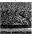
- FIGS. 7 to 8 are SEM images of an intermediate layer manufactured according to one embodiment of the present invention.
- FIG. 9 is a graph showing a change in resistance of the intermediate layer shown in FIGS. 7 and 8 .
- FIG. 10 is a perspective view of a pressure sensor according to one embodiment of the present invention.
- FIG. 11 is a cross-sectional view of a pressure sensor according to another embodiment of the present invention.
- FIG. 12 is a block diagram of a pressure sensing device according to one embodiment of the present invention.
- FIG. 13 shows an example in which the pressure sensing device according to one embodiment of the present invention is applied to a pressure sensing chair.
- FIG. 14 shows an example in which the pressure sensing device according to one embodiment of the present invention is applied to a pressure sensing mat.
- FIG. 1 is a perspective view of a pressure sensor according to one embodiment of the present invention
- FIG. 2 is an enlarged view of an intermediate layer of the pressure sensor according to one embodiment of the present invention.
- a pressure sensor 100 includes a first electrode layer 110 , a second electrode layer 120 , and an intermediate layer 130 disposed between the first electrode layer 110 and the second electrode layer 120 .
- the first electrode layer 110 and the second electrode layer 120 are made of fabric and may be made of fabric including conductive fiber.
- the conductive fiber may be a metal wire or general fiber of which the surface is covered with a metal film.
- the conductive fiber may be a general fiber in which metal particles are dispersed.
- a diameter of the metal wire may be in a range of 10 to 500 ⁇ m.
- the metal wire may be made of Cu, Ni, or a stainless alloy.
- the stainless alloy may be a martensitic stainless alloy, a ferrite-based stainless alloy, an austenite-based stainless alloy, a two-phase-based stainless alloy, a precipitation hardening-based stainless alloy, or the like.
- the metal wire is made of a stainless alloy, a corrosion resistance of the pressure sensor 100 can be increased.
- the metal film may be formed by a method of covering a surface of the general fiber with metal particles in a plating method or a deposition method.
- the metal particles may be Cu, Ni, or a stainless alloy, and a thickness of metal film may be in a range of 1 to 50 ⁇ m.
- a thickness of the metal film is less than 1 ⁇ m, a loss may be caused due to a low conductivity rate when a signal is transferred, and, when a thickness of metal film is greater than 50 ⁇ m, the metal film is easily detached from a surface of the fiber.
- the first electrode layer 110 and the second electrode layer 120 may be a plating electrode or a printing electrode and may be a flexible and elastic electrode.
- the first electrode layer 110 and the second electrode layer 120 may be formed in different directions from each other, and a crossing point may act as one sensing point. Therefore, when the sensing point is pressurized, a gap between the first electrode layer 110 and the second electrode layer 120 , that is, a thickness of intermediate layer 130 , is decreased. As applying force is increased, the thickness of intermediate layer 130 is decreased, and a piezo resistance is lowered. Therefore, the pressure sensor 100 according to the embodiment of the present invention may detect a weight according to a change in piezo resistance.
- the first electrode layer 110 may be formed to be larger than the second electrode layer 120 .
- the intermediate layer 130 includes a foam in which porous regions 134 are dispersed in a non-porous region 132 and a conductive material 136 dispersed in the foam and having a conductivity rate that is higher than that of the foam.
- the non-porous region 132 of the foam may include at least one selected from the group consisting of polyurethane, polyolefin, rubber, silicone, and elastomer.
- the intermediate layer 130 may include elasticity. Therefore, when a pressure is applied to a point at which the first electrode layer 110 and the second electrode layer 120 cross each other, a thickness of intermediate layer 130 is decreased, and a piezo resistance is changed. In this case, the porous regions 134 may be dispersed in the non-porous region 132 of the foam.
- a ratio of the porous regions 134 to the foam may be in a range of 5% to 90%.
- the ratio of the porous regions 134 to the foam is less than 5%, deformation of thickness is small, and thus a change in piezo-resistance is not measured, or weight detection recognition is hard.
- the ratio of the porous regions 134 to the foam is greater than 90%, the elastic restoring force of the foam is degraded, and thus the performance of the pressure sensor is not secured.
- the conductive material 136 in the foam may be selected from the group consisting of Au, Ag, Cu, Ni, carbon nano tubes (CNTs), carbon black, graphene, a ceramic material, and a conductive polymer.
- the conductive polymer may include polyaniline or polypyrrole.
- the ceramic material may be, for example, micro carbon coil barium titanate with a diameter of less than or equal to 100 ⁇ m. Therefore, the intermediate layer 130 has an insulation performance having a resistance of greater than or equal to 1 k ⁇ in a normal state, but when a physical change around the intermediate layer 130 is caused, or a pressure is applied to the intermediate layer 130 , a resistance is changed by a change in any one of a thickness and volume of the intermediate layer 130 .
- the conductive material 136 may be included in an amount of 1 to 10 wt % of the foam.
- the conductive material 136 is included in an amount of less than 1 wt % of the foam, piezo resistance may be caused to be insensitive to change when a pressure is applied.
- the conductive material 136 is included in an amount of greater than 10 wt % of the foam, it is hard to secure the insulation performance of the intermediate layer 130 in a state in which a pressure is not applied.
- At least a part of the conductive material 136 is dispersed in the non-porous region 132 , is dispersed to pass through an interface between the non-porous region 132 and the porous region 134 , or is dispersed in the porous region 134 . Therefore, when the conductive material 136 is dispersed in the non-porous region 132 or dispersed to pass through an interface between the non-porous region 132 and the porous region 134 , the conductive material 136 may be fixed to the inside of the foam. Therefore, even when the pressure sensor 100 is repeatedly used for a long period of time, a possibility of the conductive material 136 being detached from the foam may be decreased.
- a ratio of conductive materials dispersed in the non-porous region 132 or dispersed to pass through an interface between the non-porous region 132 and the porous region 134 to all conductive materials may be greater than or equal to 50 wt %.
- the ratio of conductive materials dispersed in the non-porous region 132 or dispersed to pass through an interface between the non-porous region 132 and the porous region 134 to all conductive materials is less than 50 wt %, pollution may occur due to detachment of the conductive material, or sensitivity to a resistance change may be degraded.
- FIG. 3 is a flowchart showing a method of manufacturing the pressure sensor according to one embodiment of the present invention.
- the foam and the conductive material are mixed (S 100 ).
- the foam may include at least one selected from the group consisting of polyurethane, polyolefin, rubber, silicone, and elastomer
- the conductive material may be selected from the group consisting of Au, Ag, Cu, Ni, CNTs, carbon black, a ceramic material, and a conductive polymer.
- the conductive material may be included in an amount of 1 to 10 wt % of the foam.
- the mixed foam and conductive material is foam-molded to form an intermediate layer (S 110 ). Therefore, the foam may be divided into the non-porous region and the porous region, and the conductive material is dispersed in the non-porous region or dispersed to pass through an interface between the non-porous region and the porous region.
- an electrode layer is attached to the intermediate layer (S 120 ).
- a first electrode layer may be attached to one surface of the intermediate layer, and a second electrode layer may be attached to the other surface of the intermediate layer.
- the intermediate layer, the first electrode layer, and the second electrode layer may be attached by an adhesive layer.
- the adhesive layer may be an insulating adhesive layer including an insulating material.
- FIGS. 4 and 5 are scanning electron microscope (SEM) images of an intermediate layer manufactured according to a comparative example
- FIG. 6 is a graph showing a change in resistance of the intermediate layer shown in FIGS. 4 and 5
- FIGS. 7 to 8 are SEM images of an intermediate layer manufactured according to one embodiment of the present invention
- FIG. 9 is a graph showing a change in resistance of the intermediate layer shown in FIGS. 7 and 8 .
- an intermediate layer was manufactured by a method in which a foam was foam-molded and was immerged in a solution including a conductive material.
- an intermediate layer was manufactured by a method in which a foam and a conductive material were mixed and foam-molded.
- the foams used in the comparative example and the embodiment were polyurethane, the conductive materials were CNTs, and the conductive materials were added in an amount of 0.05 to 3 wt % of all conductive materials.
- Resistance changes of the intermediate layer were repeatedly measured by performing a process of increasing a pressure from 0 to 1000 kPa at least three times.
- a film made of a conductive material was formed on a surface of the non-porous region of the intermediate layer manufactured according to the comparative example, but the conductive material was partially buried in the surface of the non-porous region of the intermediate layer manufactured according to the embodiment.
- the foam was foam-molded and immerged in a conductive solution, and thus most of the conductive materials were attached to a surface of the non-porous region of the foam.
- the foam and the conductive material were mixed and foam-molded, and thus the conductive materials were dispersed in the non-porous region or dispersed to pass through an interface between the non-porous region and the porous region.
- the intermediate layer manufactured according to the comparative example had resistance values which increased from first pressurization toward third pressurization, but the intermediate layer manufactured according to the embodiment had similar resistance values in the first, second, and third pressurization. Therefore, it can be confirmed that the repeatability and reproducibility of the intermediate layer manufactured according to the embodiment was higher than the repeatability and reproducibility of the intermediate layer manufactured according to the comparative example.
- an initial resistance of the intermediate layer manufactured according to the embodiment was higher than an initial resistance of the intermediate layer manufactured according to the comparative example.
- the initial resistance was high, an insulation performance in a state in which a pressure was not applied was excellent, and current consumption of a sensor could be decreased.
- FIG. 10 is a perspective view of a pressure sensor according to one embodiment of the present invention. The same descriptions as those in the first to third embodiments will be omitted.
- a pressure sensor 100 includes a first electrode layer 110 including a first conductive region 112 , a second electrode layer 120 including a second conductive region 122 , and an intermediate layer 130 disposed between the first electrode layer 110 and the second electrode layer 120 .
- the first electrode layer 110 and the second electrode layer 120 are made of fabric, and the first conductive region 112 and the second conductive region 122 may be made of fabric including conductive fiber.
- the first conductive region 112 of the first electrode layer 110 and the second conductive region 122 of the second electrode layer 120 may be formed in different directions from each other, and a point at which the first conductive region 112 and the second conductive region 122 cross each other may act as one sensing point. Therefore, when the sensing point is pressurized, a gap between the first conductive region 112 and the second conductive region 122 , that is, a thickness of the intermediate layer 130 , is decreased. As applying force is increased, a thickness of the intermediate layer 130 is decreased, and a piezo resistance is lowered. Therefore, the present invention pressure sensor 100 according to the embodiment may detect a weight according to a change in piezo resistance.
- first conductive region 112 may be formed to be larger than the second conductive region 122 , and a plurality of second conductive regions 122 may be disposed on one first conductive region 112 .
- the intermediate layer between the first electrode layer and the second electrode layer is formed has been mainly described, and the first electrode layer and the second electrode layer may be disposed to be coplanar.
- FIG. 11 is a cross-sectional view of a pressure sensor according to another embodiment of the present invention. The same descriptions as those in the first to third embodiments will be omitted.
- a pressure sensor 100 includes a first electrode layer 110 including a first conductive region, a second electrode layer 120 including a second conductive region, and an intermediate layer 130 .
- the second electrode layer 120 is disposed to be spaced apart from the first electrode layer 110 on a horizontal surface, and the intermediate layer 130 may be disposed on or under the first electrode layer 110 and the second electrode layer 120 .
- a ground may be connected to one layer, and it is not necessary to install an additional ground electrode, and thus costs for materials of the pressure sensor 100 and manufacturing the pressure sensor 100 can be reduced, and a thickness of the pressure sensor 100 can be reduced.
- the first electrode layer 110 and the second electrode layer 120 may be attached to the intermediate layer 130 through an adhesive layer 140 .
- the adhesive layer 140 includes an insulator and may be disposed on one area between the first electrode layer 110 and the intermediate layer 130 and on one area between the second electrode layer 120 and the intermediate layer 130 .
- the adhesive layer 140 may be separately disposed in the same manner as the first electrode layer 110 and the second electrode layer 120 . Further, the adhesive layer 140 may have a structure in which both surfaces of the film are coated with insulating adhesives.
- a thickness of the elastic intermediate layer 130 is changed. Due to a change in thickness of the intermediate layer 130 , the first electrode layer 110 and the second electrode layer 120 spaced apart from each other are connected to allow electricity to flow. A level of pressure may be detected based on a generated electric signal.
- the pressure sensor according to the embodiment of the present invention may be included in the pressure sensing device.
- FIG. 12 is a block diagram of a pressure sensing device according to one embodiment of the present invention.
- a pressure sensing device 200 includes a pressure sensor 100 , a signal processing unit 210 , a control unit 220 , and a communication unit 230 .
- the pressure sensor 100 may generate an electric signal due to a resistance change caused by change in at least one of a thickness and a volume of the intermediate layer 130 .
- Electric signals of the first electrode layer 110 and the second electrode layer 120 are transmitted to the signal processing unit 210 .
- the first electrode layer 110 , the second electrode layer 120 , and the signal processing unit 210 may be connected by a flexible printed circuit board (FPCB).
- FPCB flexible printed circuit board
- the signal processing unit 210 processes the electric signals received from the first electrode layer 110 and the second electrode layer 120 and transmits the electric signals to the control unit 220 , and the control unit 220 may generate a control signal based on a signal processed by the signal processing unit 210 .
- the control unit 220 may control the pressure sensing device 200 to turn on/off using a result obtained by processing a signal detected by the pressure sensor 100 .
- the control unit 220 may generate diagnosis information using the result obtained by processing the signal detected by the pressure sensor 100 .
- the control unit 220 may generate an alarm signal and the like for a user using the result obtained by processing the signal detected by the pressure sensor 100 .
- the communication unit 230 transmits a control signal generated by the control unit 220 to an external device.
- the pressure sensor 100 is disposed in a separate space from the signal processing unit 210 , the control unit 220 , and the communication unit 230 and may be connected through the FPCB. Otherwise, the pressure sensor 100 is disposed in the same space as the signal processing unit 210 , the control unit 220 , and the communication unit 230 and may be connected through the FPCB.
- the pressure sensor 100 may be applied to various application fields using body pressure distribution such as a pressure detection insole, a pressure detection grove, a pressure detecting mat, a pressure detecting chair, and the like.
- FIG. 13 shows an example in which the pressure sensing device according to one embodiment of the present invention is applied to a pressure sensing chair.
- a pressure sensing chair 1200 includes a seat 1210 , an armrest 1220 , a backrest 1230 , a leg 1240 , and the like.
- the pressure sensing device 200 embedded in the pressure sensing chair 1200 detects whether a user is seated and may measure relative pressure distribution according to seating of the user.
- the pressure sensing device 200 may detect a weight, an age group, and a sitting position, and the like according to the measured pressure distribution.
- the pressure sensor 100 according to the embodiment of the present invention may be installed in the seat 1210 .
- FIG. 14 shows an example in which the pressure sensing device according to one embodiment of the present invention is applied to a pressure sensing mat.
- the pressure sensor 100 is included in a mat 1300 , and the signal processing unit 210 , the control unit 220 , and the communication unit 230 of the pressure sensing device 200 may be disposed in a separate space.
- the pressure sensor 100 included in the mat 1300 detects a change in piezo resistance, and the control unit 220 may measure a weight applied to the mat 1300 based on the detected change in piezo resistance.
- the control unit 220 locks an home appliance, a gas range, or the like around the mat or may generate a control signal for outputting an alarm.
Landscapes
- Physics & Mathematics (AREA)
- General Physics & Mathematics (AREA)
- Chemical & Material Sciences (AREA)
- Dispersion Chemistry (AREA)
- Spectroscopy & Molecular Physics (AREA)
- Force Measurement Appropriate To Specific Purposes (AREA)
Abstract
Description
-
- 100: PRESSURE SENSOR
- 110: FIRST ELECTRODE LAYER
- 120: SECOND ELECTRODE LAYER
- 130: INTERMEDIATE LAYER
- 132: NON-POROUS REGION
- 134: POROUS REGION
- 136: CONDUCTIVE MATERIAL
Claims (20)
Applications Claiming Priority (3)
| Application Number | Priority Date | Filing Date | Title |
|---|---|---|---|
| KR1020160082982A KR101753247B1 (en) | 2016-06-30 | 2016-06-30 | Pressure sensing sensor and pressure sensing apparatus comprising the same |
| KR10-2016-0082982 | 2016-06-30 | ||
| PCT/KR2016/007493 WO2018004049A1 (en) | 2016-06-30 | 2016-07-11 | Pressure sensor and pressure sensing device comprising same |
Publications (2)
| Publication Number | Publication Date |
|---|---|
| US20190219460A1 US20190219460A1 (en) | 2019-07-18 |
| US11029222B2 true US11029222B2 (en) | 2021-06-08 |
Family
ID=59357033
Family Applications (1)
| Application Number | Title | Priority Date | Filing Date |
|---|---|---|---|
| US16/313,110 Active US11029222B2 (en) | 2016-06-30 | 2016-07-11 | Pressure sensor having conductive material extending between non-porous and porous regions and pressure sensing device comprising same |
Country Status (3)
| Country | Link |
|---|---|
| US (1) | US11029222B2 (en) |
| KR (1) | KR101753247B1 (en) |
| WO (1) | WO2018004049A1 (en) |
Cited By (2)
| Publication number | Priority date | Publication date | Assignee | Title |
|---|---|---|---|---|
| US11320327B2 (en) * | 2019-07-18 | 2022-05-03 | Medx Technology Inc. | Pressure sensing device and manufacturing method thereof |
| US12173133B2 (en) | 2021-12-30 | 2024-12-24 | Hyundai Motor Company | Preparing method for conductive composite, conductive composite and piezoresistive device using the same |
Families Citing this family (11)
| Publication number | Priority date | Publication date | Assignee | Title |
|---|---|---|---|---|
| CN107782475B (en) * | 2017-10-24 | 2020-08-11 | 北京石墨烯研究院 | Resistive pressure sensor and preparation method |
| WO2019129387A1 (en) * | 2018-01-01 | 2019-07-04 | Rhodia Operations | Structured composites useful as low force sensors |
| JP7026238B2 (en) * | 2018-01-01 | 2022-02-25 | ローディア オペレーションズ | Devices including pressure sensitive layers and pressure sensitive layers |
| JP2021513580A (en) * | 2018-01-01 | 2021-05-27 | ローディア オペレーションズ | Structured composition useful as a low force sensor |
| WO2019221536A1 (en) * | 2018-05-18 | 2019-11-21 | 동우화인켐 주식회사 | Pressure sensor and image display device including same |
| JP2020046391A (en) * | 2018-09-21 | 2020-03-26 | 藤倉コンポジット株式会社 | Pressure sensor |
| US20230228633A1 (en) * | 2020-06-18 | 2023-07-20 | Basf Se | Piezoresistive Pressure Sensor Based on Foam Structure |
| CN112697034A (en) * | 2021-03-25 | 2021-04-23 | 湖南大学 | Flexible strain sensor made of graphene composite material and preparation method of flexible strain sensor |
| US12056305B2 (en) * | 2022-01-05 | 2024-08-06 | Samsung Electronics Co., Ltd. | Pressure sensor, pressure sensor pixel array including pressure sensor, and electronic system including pressure sensor |
| CN118283469A (en) * | 2022-12-30 | 2024-07-02 | 华为技术有限公司 | Electronic device and method for coating material |
| CN220935157U (en) * | 2023-09-28 | 2024-05-10 | 童宗伟 | A pressure sensor device with body sensing and body sensing pressure switch |
Citations (52)
| Publication number | Priority date | Publication date | Assignee | Title |
|---|---|---|---|---|
| US3398233A (en) * | 1965-04-20 | 1968-08-20 | Dennis G Wyman | Electrical conductor of fibers embedded in an insulator |
| US4258100A (en) * | 1977-09-09 | 1981-03-24 | Kabushiki Kaisha Kyowa | Pressure-sensitive electric conductive sheet material |
| US4449774A (en) * | 1981-02-05 | 1984-05-22 | Shin-Etsu Polymer Co., Ltd. | Electroconductive rubbery member and elastic connector therewith |
| US4876419A (en) * | 1987-06-02 | 1989-10-24 | Leda Logarithmic Electrical Devices For Automation S.R.L. | Two-dimensional electric conductor designed to function as an electric switch |
| US4876420A (en) * | 1987-06-02 | 1989-10-24 | Leda Logarithmic Electrical Devices For Automation S.R.L. | Continuous flexible electric conductor capable of functioning as an electric switch |
| US4900497A (en) * | 1987-02-05 | 1990-02-13 | Leda Logarithmic Electrical Devices For Automation S.R.L. | Process for producing electric resistors having a wide range of specific resistance values |
| US4977386A (en) * | 1987-10-13 | 1990-12-11 | Leda Logarithmic Electrical Devices For Automation S.R.L. | Electric resistor producible in a wide range of specific resistance values, and relative manufacturing process |
| US5060527A (en) * | 1990-02-14 | 1991-10-29 | Burgess Lester E | Tactile sensing transducer |
| US5213715A (en) * | 1989-04-17 | 1993-05-25 | Western Digital Corporation | Directionally conductive polymer |
| US5431571A (en) * | 1993-11-22 | 1995-07-11 | W. L. Gore & Associates, Inc. | Electrical conductive polymer matrix |
| US5679888A (en) * | 1994-10-05 | 1997-10-21 | Matsushita Electric Industrial Co., Ltd. | Dynamic quantity sensor and method for producing the same, distortion resistance element and method for producing the same, and angular velocity sensor |
| US5695859A (en) * | 1995-04-27 | 1997-12-09 | Burgess; Lester E. | Pressure activated switching device |
| US5904978A (en) * | 1995-12-15 | 1999-05-18 | W. L. Gore & Associates, Inc. | Electrically conductive polytetrafluoroethylene article |
| US6114645A (en) * | 1995-04-27 | 2000-09-05 | Burgess; Lester E. | Pressure activated switching device |
| US6210789B1 (en) * | 1997-02-20 | 2001-04-03 | W. L. Gore & Associates, Inc. | Electrically conductive composite article |
| US6238599B1 (en) * | 1997-06-18 | 2001-05-29 | International Business Machines Corporation | High conductivity, high strength, lead-free, low cost, electrically conducting materials and applications |
| US6452479B1 (en) * | 1999-05-20 | 2002-09-17 | Eleksen Limited | Detector contructed from fabric |
| US6501463B1 (en) * | 1999-12-10 | 2002-12-31 | Siemens Technology -To-Business Center Llc | Electronic whiteboard system using a tactile foam sensor |
| US6534430B2 (en) * | 2000-02-28 | 2003-03-18 | Kabushiki Kaisha Toyota Chuo Kenkyusho | Material for measuring static and dynamic physical parameters |
| US6646540B1 (en) * | 1999-06-22 | 2003-11-11 | Peratech Limited | Conductive structures |
| US20030213939A1 (en) * | 2002-04-01 | 2003-11-20 | Sujatha Narayan | Electrically conductive polymeric foams and elastomers and methods of manufacture thereof |
| US6724195B2 (en) * | 2002-03-29 | 2004-04-20 | Jerome R. Lurtz | Contact sensor |
| US6809280B2 (en) * | 2002-05-02 | 2004-10-26 | 3M Innovative Properties Company | Pressure activated switch and touch panel |
| US6835889B2 (en) * | 2001-09-21 | 2004-12-28 | Kabushiki Kaisha Toshiba | Passive element component and substrate with built-in passive element |
| US6888537B2 (en) * | 2002-02-13 | 2005-05-03 | Siemens Technology-To-Business Center, Llc | Configurable industrial input devices that use electrically conductive elastomer |
| US7260999B2 (en) * | 2004-12-23 | 2007-08-28 | 3M Innovative Properties Company | Force sensing membrane |
| US7443082B2 (en) * | 2006-03-03 | 2008-10-28 | Basf Corporation | Piezoelectric polymer composite article and system |
| US20090002201A1 (en) * | 1993-07-29 | 2009-01-01 | Research Transfer Enterprise, L.L.C. | Keyboard with keys for moving cursor |
| US7594442B2 (en) * | 2005-10-14 | 2009-09-29 | T-Ink Tc Corp | Resistance varying sensor using electrically conductive coated materials |
| US7703333B2 (en) * | 2006-09-15 | 2010-04-27 | Tokai Rubber Industries, Ltd. | Deformation sensor |
| JP2010101827A (en) | 2008-10-27 | 2010-05-06 | Kuraray Co Ltd | Pressure detector |
| US8089336B2 (en) * | 2007-05-02 | 2012-01-03 | Peratech Limited | Position detection |
| US8253696B2 (en) * | 2006-10-23 | 2012-08-28 | Patrick R. Antaki | Flexible fingerprint sensor |
| US8371174B2 (en) * | 2009-08-31 | 2013-02-12 | Universal Cement Corporation | Micro-deformable piezoresistive material and manufacturing method thereof and pressure sensor using the same |
| US8471719B2 (en) * | 2010-01-22 | 2013-06-25 | Tsinghua University | Pressure control switch, method for using the same and alarm system using the same |
| US8514088B2 (en) * | 2010-01-22 | 2013-08-20 | Tsinghua University | Temperature control switch, method for using the same and alarm system using the same |
| US8558434B2 (en) * | 2010-12-22 | 2013-10-15 | Canon Kabushiki Kaisha | Actuator |
| US8570641B2 (en) * | 2010-10-28 | 2013-10-29 | Seiko Epson Corporation | Display sheet, display device, and electronic apparatus |
| US8669755B2 (en) * | 2010-08-02 | 2014-03-11 | Sony Corporation | Geometry sensor and information input device |
| US20140090489A1 (en) | 2012-09-29 | 2014-04-03 | Stryker Corporation | Force detecting mat with multiple sensor types |
| KR20150007855A (en) | 2013-07-12 | 2015-01-21 | 강진규 | Pressure sensor |
| US8984954B2 (en) * | 2013-03-15 | 2015-03-24 | Brigham Young University | Composite material used as a strain gauge |
| WO2016010894A1 (en) | 2014-07-14 | 2016-01-21 | Rogers Corporation | Foam pressure sensor |
| US9448127B2 (en) * | 2011-01-13 | 2016-09-20 | Francis Cannard | Device for measuring pressure from a flexible, pliable, and/or extensible object made from a textile material comprising a measurement device |
| US9743712B2 (en) * | 2015-05-28 | 2017-08-29 | Nike, Inc. | Sole structure with electrically controllable damping element |
| US9857246B2 (en) * | 2014-09-17 | 2018-01-02 | Sensable Technologies, Llc | Sensing system including a sensing membrane |
| US9904393B2 (en) * | 2010-06-11 | 2018-02-27 | 3M Innovative Properties Company | Positional touch sensor with force measurement |
| US20180198129A1 (en) * | 2015-10-28 | 2018-07-12 | Lg Chem, Ltd. | Conductive material dispersed liquid and lithium secondary battery manufactured using the same |
| US20180326456A1 (en) * | 2015-11-06 | 2018-11-15 | Moda-Innochips Co., Ltd. | Pressure sensor, and composite element and electronic device having same |
| US10260968B2 (en) * | 2013-03-15 | 2019-04-16 | Nano Composite Products, Inc. | Polymeric foam deformation gauge |
| US10401238B2 (en) * | 2014-02-26 | 2019-09-03 | 3M Innovative Properties Company | Force responsive inductors for force sensors |
| US10418145B2 (en) * | 2014-06-06 | 2019-09-17 | President And Fellows Of Harvard College | Stretchable conductive composites for use in soft devices |
Family Cites Families (2)
| Publication number | Priority date | Publication date | Assignee | Title |
|---|---|---|---|---|
| US8966997B2 (en) * | 2011-10-12 | 2015-03-03 | Stryker Corporation | Pressure sensing mat |
| JP2015187561A (en) | 2014-03-26 | 2015-10-29 | 株式会社日本自動車部品総合研究所 | Pressure sensor |
-
2016
- 2016-06-30 KR KR1020160082982A patent/KR101753247B1/en not_active Expired - Fee Related
- 2016-07-11 US US16/313,110 patent/US11029222B2/en active Active
- 2016-07-11 WO PCT/KR2016/007493 patent/WO2018004049A1/en active Application Filing
Patent Citations (61)
| Publication number | Priority date | Publication date | Assignee | Title |
|---|---|---|---|---|
| US3398233A (en) * | 1965-04-20 | 1968-08-20 | Dennis G Wyman | Electrical conductor of fibers embedded in an insulator |
| US4258100A (en) * | 1977-09-09 | 1981-03-24 | Kabushiki Kaisha Kyowa | Pressure-sensitive electric conductive sheet material |
| US4449774A (en) * | 1981-02-05 | 1984-05-22 | Shin-Etsu Polymer Co., Ltd. | Electroconductive rubbery member and elastic connector therewith |
| US4900497A (en) * | 1987-02-05 | 1990-02-13 | Leda Logarithmic Electrical Devices For Automation S.R.L. | Process for producing electric resistors having a wide range of specific resistance values |
| US4876419A (en) * | 1987-06-02 | 1989-10-24 | Leda Logarithmic Electrical Devices For Automation S.R.L. | Two-dimensional electric conductor designed to function as an electric switch |
| US4876420A (en) * | 1987-06-02 | 1989-10-24 | Leda Logarithmic Electrical Devices For Automation S.R.L. | Continuous flexible electric conductor capable of functioning as an electric switch |
| US4977386A (en) * | 1987-10-13 | 1990-12-11 | Leda Logarithmic Electrical Devices For Automation S.R.L. | Electric resistor producible in a wide range of specific resistance values, and relative manufacturing process |
| US5213715A (en) * | 1989-04-17 | 1993-05-25 | Western Digital Corporation | Directionally conductive polymer |
| US5060527A (en) * | 1990-02-14 | 1991-10-29 | Burgess Lester E | Tactile sensing transducer |
| US20090002201A1 (en) * | 1993-07-29 | 2009-01-01 | Research Transfer Enterprise, L.L.C. | Keyboard with keys for moving cursor |
| US5431571A (en) * | 1993-11-22 | 1995-07-11 | W. L. Gore & Associates, Inc. | Electrical conductive polymer matrix |
| US5679888A (en) * | 1994-10-05 | 1997-10-21 | Matsushita Electric Industrial Co., Ltd. | Dynamic quantity sensor and method for producing the same, distortion resistance element and method for producing the same, and angular velocity sensor |
| US5695859A (en) * | 1995-04-27 | 1997-12-09 | Burgess; Lester E. | Pressure activated switching device |
| US5828289A (en) * | 1995-04-27 | 1998-10-27 | Burgess; Lester E. | Pressure activated switching device |
| US5886615A (en) * | 1995-04-27 | 1999-03-23 | Burgess; Lester E. | Pressure activated switching device with piezoresistive material |
| US5910355A (en) * | 1995-04-27 | 1999-06-08 | Burgess; Lester E. | Pressure activated switching device |
| US5962118A (en) * | 1995-04-27 | 1999-10-05 | Burgess; Lester E. | Pressure activated switching device |
| US6072130A (en) * | 1995-04-27 | 2000-06-06 | Burgess; Lester E. | Pressure activated switching device |
| US6114645A (en) * | 1995-04-27 | 2000-09-05 | Burgess; Lester E. | Pressure activated switching device |
| US5904978A (en) * | 1995-12-15 | 1999-05-18 | W. L. Gore & Associates, Inc. | Electrically conductive polytetrafluoroethylene article |
| US6210789B1 (en) * | 1997-02-20 | 2001-04-03 | W. L. Gore & Associates, Inc. | Electrically conductive composite article |
| US6238599B1 (en) * | 1997-06-18 | 2001-05-29 | International Business Machines Corporation | High conductivity, high strength, lead-free, low cost, electrically conducting materials and applications |
| US6452479B1 (en) * | 1999-05-20 | 2002-09-17 | Eleksen Limited | Detector contructed from fabric |
| US6714117B2 (en) * | 1999-05-20 | 2004-03-30 | Eleksen Limited | Detector constructed from fabric |
| US6646540B1 (en) * | 1999-06-22 | 2003-11-11 | Peratech Limited | Conductive structures |
| US6501463B1 (en) * | 1999-12-10 | 2002-12-31 | Siemens Technology -To-Business Center Llc | Electronic whiteboard system using a tactile foam sensor |
| US6534430B2 (en) * | 2000-02-28 | 2003-03-18 | Kabushiki Kaisha Toyota Chuo Kenkyusho | Material for measuring static and dynamic physical parameters |
| US6835889B2 (en) * | 2001-09-21 | 2004-12-28 | Kabushiki Kaisha Toshiba | Passive element component and substrate with built-in passive element |
| US6888537B2 (en) * | 2002-02-13 | 2005-05-03 | Siemens Technology-To-Business Center, Llc | Configurable industrial input devices that use electrically conductive elastomer |
| US6724195B2 (en) * | 2002-03-29 | 2004-04-20 | Jerome R. Lurtz | Contact sensor |
| US20030213939A1 (en) * | 2002-04-01 | 2003-11-20 | Sujatha Narayan | Electrically conductive polymeric foams and elastomers and methods of manufacture thereof |
| US6809280B2 (en) * | 2002-05-02 | 2004-10-26 | 3M Innovative Properties Company | Pressure activated switch and touch panel |
| US7260999B2 (en) * | 2004-12-23 | 2007-08-28 | 3M Innovative Properties Company | Force sensing membrane |
| US7594442B2 (en) * | 2005-10-14 | 2009-09-29 | T-Ink Tc Corp | Resistance varying sensor using electrically conductive coated materials |
| US7443082B2 (en) * | 2006-03-03 | 2008-10-28 | Basf Corporation | Piezoelectric polymer composite article and system |
| US7703333B2 (en) * | 2006-09-15 | 2010-04-27 | Tokai Rubber Industries, Ltd. | Deformation sensor |
| US8253696B2 (en) * | 2006-10-23 | 2012-08-28 | Patrick R. Antaki | Flexible fingerprint sensor |
| US8363028B2 (en) * | 2006-10-23 | 2013-01-29 | Antaki Patrick R | Flexible fingerprint sensor |
| US8089336B2 (en) * | 2007-05-02 | 2012-01-03 | Peratech Limited | Position detection |
| JP2010101827A (en) | 2008-10-27 | 2010-05-06 | Kuraray Co Ltd | Pressure detector |
| US8371174B2 (en) * | 2009-08-31 | 2013-02-12 | Universal Cement Corporation | Micro-deformable piezoresistive material and manufacturing method thereof and pressure sensor using the same |
| US8471719B2 (en) * | 2010-01-22 | 2013-06-25 | Tsinghua University | Pressure control switch, method for using the same and alarm system using the same |
| US8514088B2 (en) * | 2010-01-22 | 2013-08-20 | Tsinghua University | Temperature control switch, method for using the same and alarm system using the same |
| US9904393B2 (en) * | 2010-06-11 | 2018-02-27 | 3M Innovative Properties Company | Positional touch sensor with force measurement |
| US8669755B2 (en) * | 2010-08-02 | 2014-03-11 | Sony Corporation | Geometry sensor and information input device |
| US8570641B2 (en) * | 2010-10-28 | 2013-10-29 | Seiko Epson Corporation | Display sheet, display device, and electronic apparatus |
| US8558434B2 (en) * | 2010-12-22 | 2013-10-15 | Canon Kabushiki Kaisha | Actuator |
| US9448127B2 (en) * | 2011-01-13 | 2016-09-20 | Francis Cannard | Device for measuring pressure from a flexible, pliable, and/or extensible object made from a textile material comprising a measurement device |
| US20140090489A1 (en) | 2012-09-29 | 2014-04-03 | Stryker Corporation | Force detecting mat with multiple sensor types |
| US10260968B2 (en) * | 2013-03-15 | 2019-04-16 | Nano Composite Products, Inc. | Polymeric foam deformation gauge |
| US8984954B2 (en) * | 2013-03-15 | 2015-03-24 | Brigham Young University | Composite material used as a strain gauge |
| US10263174B2 (en) * | 2013-03-15 | 2019-04-16 | Nano Composite Products, Inc. | Composite material used as a strain gauge |
| KR20150007855A (en) | 2013-07-12 | 2015-01-21 | 강진규 | Pressure sensor |
| US10401238B2 (en) * | 2014-02-26 | 2019-09-03 | 3M Innovative Properties Company | Force responsive inductors for force sensors |
| US10418145B2 (en) * | 2014-06-06 | 2019-09-17 | President And Fellows Of Harvard College | Stretchable conductive composites for use in soft devices |
| WO2016010894A1 (en) | 2014-07-14 | 2016-01-21 | Rogers Corporation | Foam pressure sensor |
| US20170199095A1 (en) | 2014-07-14 | 2017-07-13 | Rogers Corporation | Foam pressure sensor |
| US9857246B2 (en) * | 2014-09-17 | 2018-01-02 | Sensable Technologies, Llc | Sensing system including a sensing membrane |
| US9743712B2 (en) * | 2015-05-28 | 2017-08-29 | Nike, Inc. | Sole structure with electrically controllable damping element |
| US20180198129A1 (en) * | 2015-10-28 | 2018-07-12 | Lg Chem, Ltd. | Conductive material dispersed liquid and lithium secondary battery manufactured using the same |
| US20180326456A1 (en) * | 2015-11-06 | 2018-11-15 | Moda-Innochips Co., Ltd. | Pressure sensor, and composite element and electronic device having same |
Non-Patent Citations (1)
| Title |
|---|
| International Search Report (with English Translation) and Written Opinion dated Mar. 20, 2017 issued in Application No. PCT/KR2016/007493. |
Cited By (2)
| Publication number | Priority date | Publication date | Assignee | Title |
|---|---|---|---|---|
| US11320327B2 (en) * | 2019-07-18 | 2022-05-03 | Medx Technology Inc. | Pressure sensing device and manufacturing method thereof |
| US12173133B2 (en) | 2021-12-30 | 2024-12-24 | Hyundai Motor Company | Preparing method for conductive composite, conductive composite and piezoresistive device using the same |
Also Published As
| Publication number | Publication date |
|---|---|
| KR101753247B1 (en) | 2017-07-04 |
| US20190219460A1 (en) | 2019-07-18 |
| WO2018004049A1 (en) | 2018-01-04 |
Similar Documents
| Publication | Publication Date | Title |
|---|---|---|
| US11029222B2 (en) | Pressure sensor having conductive material extending between non-porous and porous regions and pressure sensing device comprising same | |
| CN108135362B (en) | pressure sensing chair | |
| US10876907B2 (en) | Pressure detection sensor having a plurality of dielectric layers and a plurality of electrode layers with conductive paths and wiring portions | |
| KR102361874B1 (en) | Pressure sensing sensor and pressure sensing apparatus comprising the same | |
| KR102382320B1 (en) | Pressure sensor device | |
| KR20180117893A (en) | Pressure sensor | |
| KR102361875B1 (en) | Pressure sensing sensor and pressure sensing apparatus comprising the same | |
| WO2021254249A1 (en) | Piezoresistive pressure sensor based on foam structure | |
| KR101783413B1 (en) | Sensor for detecting pressure and insole of sensing pressure including the same | |
| KR20180117889A (en) | Pressure sensor | |
| JP6829365B2 (en) | Pressure sensors, pressure sensor manufacturing methods, bed devices and automotive seats | |
| JP2008256399A (en) | Pressure sensitive resistance element | |
| US20200260815A1 (en) | Pressure sensing insole | |
| US10794779B2 (en) | Pressure sensor | |
| KR20170040985A (en) | Chair of sensing pressure | |
| KR20180117894A (en) | Pressure sensing sensor and pressure sensing apparatus comprising the same | |
| KR20180053133A (en) | Humidity sensor | |
| KR20170131988A (en) | Sensor for detecting pressure and insol of sensing pressure including the same | |
| KR102308301B1 (en) | Pressure sensing sensor and pressure sensing apparatus comprising the same | |
| KR20170081482A (en) | Chair of sensing pressure | |
| KR20170074045A (en) | Chair of sensing pressure | |
| KR102461696B1 (en) | Chair of sensing pressure | |
| KR102400892B1 (en) | Pressure sensor device | |
| Atalay | Development of textile-based resistive pressure sensing structures for wearable electronic systems | |
| KR102568540B1 (en) | Sensor for detecting pressrue |
Legal Events
| Date | Code | Title | Description |
|---|---|---|---|
| FEPP | Fee payment procedure |
Free format text: ENTITY STATUS SET TO UNDISCOUNTED (ORIGINAL EVENT CODE: BIG.); ENTITY STATUS OF PATENT OWNER: LARGE ENTITY |
|
| STPP | Information on status: patent application and granting procedure in general |
Free format text: DOCKETED NEW CASE - READY FOR EXAMINATION |
|
| AS | Assignment |
Owner name: LG INNOTEK CO., LTD., KOREA, REPUBLIC OF Free format text: ASSIGNMENT OF ASSIGNORS INTEREST;ASSIGNORS:LEE, SOO MIN;CHO, IN HEE;JO, HYUN JIN;SIGNING DATES FROM 20190228 TO 20190521;REEL/FRAME:049245/0191 |
|
| STPP | Information on status: patent application and granting procedure in general |
Free format text: NON FINAL ACTION MAILED |
|
| STPP | Information on status: patent application and granting procedure in general |
Free format text: RESPONSE TO NON-FINAL OFFICE ACTION ENTERED AND FORWARDED TO EXAMINER |
|
| STPP | Information on status: patent application and granting procedure in general |
Free format text: FINAL REJECTION MAILED |
|
| STPP | Information on status: patent application and granting procedure in general |
Free format text: ADVISORY ACTION MAILED |
|
| STPP | Information on status: patent application and granting procedure in general |
Free format text: DOCKETED NEW CASE - READY FOR EXAMINATION |
|
| STPP | Information on status: patent application and granting procedure in general |
Free format text: NOTICE OF ALLOWANCE MAILED -- APPLICATION RECEIVED IN OFFICE OF PUBLICATIONS |
|
| STPP | Information on status: patent application and granting procedure in general |
Free format text: PUBLICATIONS -- ISSUE FEE PAYMENT VERIFIED |
|
| STCF | Information on status: patent grant |
Free format text: PATENTED CASE |
|
| MAFP | Maintenance fee payment |
Free format text: PAYMENT OF MAINTENANCE FEE, 4TH YEAR, LARGE ENTITY (ORIGINAL EVENT CODE: M1551); ENTITY STATUS OF PATENT OWNER: LARGE ENTITY Year of fee payment: 4 |