US11004418B2 - Display panel driving method, driving device, display device and non-transitory computer readable medium - Google Patents
Display panel driving method, driving device, display device and non-transitory computer readable medium Download PDFInfo
- Publication number
- US11004418B2 US11004418B2 US16/622,646 US201716622646A US11004418B2 US 11004418 B2 US11004418 B2 US 11004418B2 US 201716622646 A US201716622646 A US 201716622646A US 11004418 B2 US11004418 B2 US 11004418B2
- Authority
- US
- United States
- Prior art keywords
- switch transistor
- electrode
- scanning line
- pixel
- pixel electrode
- Prior art date
- Legal status (The legal status is an assumption and is not a legal conclusion. Google has not performed a legal analysis and makes no representation as to the accuracy of the status listed.)
- Active
Links
Images


Classifications
-
- G—PHYSICS
- G09—EDUCATION; CRYPTOGRAPHY; DISPLAY; ADVERTISING; SEALS
- G09G—ARRANGEMENTS OR CIRCUITS FOR CONTROL OF INDICATING DEVICES USING STATIC MEANS TO PRESENT VARIABLE INFORMATION
- G09G3/00—Control arrangements or circuits, of interest only in connection with visual indicators other than cathode-ray tubes
- G09G3/20—Control arrangements or circuits, of interest only in connection with visual indicators other than cathode-ray tubes for presentation of an assembly of a number of characters, e.g. a page, by composing the assembly by combination of individual elements arranged in a matrix no fixed position being assigned to or needed to be assigned to the individual characters or partial characters
- G09G3/34—Control arrangements or circuits, of interest only in connection with visual indicators other than cathode-ray tubes for presentation of an assembly of a number of characters, e.g. a page, by composing the assembly by combination of individual elements arranged in a matrix no fixed position being assigned to or needed to be assigned to the individual characters or partial characters by control of light from an independent source
- G09G3/36—Control arrangements or circuits, of interest only in connection with visual indicators other than cathode-ray tubes for presentation of an assembly of a number of characters, e.g. a page, by composing the assembly by combination of individual elements arranged in a matrix no fixed position being assigned to or needed to be assigned to the individual characters or partial characters by control of light from an independent source using liquid crystals
- G09G3/3611—Control of matrices with row and column drivers
- G09G3/3648—Control of matrices with row and column drivers using an active matrix
-
- G—PHYSICS
- G09—EDUCATION; CRYPTOGRAPHY; DISPLAY; ADVERTISING; SEALS
- G09G—ARRANGEMENTS OR CIRCUITS FOR CONTROL OF INDICATING DEVICES USING STATIC MEANS TO PRESENT VARIABLE INFORMATION
- G09G3/00—Control arrangements or circuits, of interest only in connection with visual indicators other than cathode-ray tubes
- G09G3/20—Control arrangements or circuits, of interest only in connection with visual indicators other than cathode-ray tubes for presentation of an assembly of a number of characters, e.g. a page, by composing the assembly by combination of individual elements arranged in a matrix no fixed position being assigned to or needed to be assigned to the individual characters or partial characters
- G09G3/34—Control arrangements or circuits, of interest only in connection with visual indicators other than cathode-ray tubes for presentation of an assembly of a number of characters, e.g. a page, by composing the assembly by combination of individual elements arranged in a matrix no fixed position being assigned to or needed to be assigned to the individual characters or partial characters by control of light from an independent source
- G09G3/36—Control arrangements or circuits, of interest only in connection with visual indicators other than cathode-ray tubes for presentation of an assembly of a number of characters, e.g. a page, by composing the assembly by combination of individual elements arranged in a matrix no fixed position being assigned to or needed to be assigned to the individual characters or partial characters by control of light from an independent source using liquid crystals
- G09G3/3611—Control of matrices with row and column drivers
- G09G3/3674—Details of drivers for scan electrodes
- G09G3/3677—Details of drivers for scan electrodes suitable for active matrices only
-
- G—PHYSICS
- G09—EDUCATION; CRYPTOGRAPHY; DISPLAY; ADVERTISING; SEALS
- G09G—ARRANGEMENTS OR CIRCUITS FOR CONTROL OF INDICATING DEVICES USING STATIC MEANS TO PRESENT VARIABLE INFORMATION
- G09G3/00—Control arrangements or circuits, of interest only in connection with visual indicators other than cathode-ray tubes
- G09G3/20—Control arrangements or circuits, of interest only in connection with visual indicators other than cathode-ray tubes for presentation of an assembly of a number of characters, e.g. a page, by composing the assembly by combination of individual elements arranged in a matrix no fixed position being assigned to or needed to be assigned to the individual characters or partial characters
- G09G3/34—Control arrangements or circuits, of interest only in connection with visual indicators other than cathode-ray tubes for presentation of an assembly of a number of characters, e.g. a page, by composing the assembly by combination of individual elements arranged in a matrix no fixed position being assigned to or needed to be assigned to the individual characters or partial characters by control of light from an independent source
- G09G3/36—Control arrangements or circuits, of interest only in connection with visual indicators other than cathode-ray tubes for presentation of an assembly of a number of characters, e.g. a page, by composing the assembly by combination of individual elements arranged in a matrix no fixed position being assigned to or needed to be assigned to the individual characters or partial characters by control of light from an independent source using liquid crystals
- G09G3/3611—Control of matrices with row and column drivers
- G09G3/3648—Control of matrices with row and column drivers using an active matrix
- G09G3/3659—Control of matrices with row and column drivers using an active matrix the addressing of the pixel involving the control of two or more scan electrodes or two or more data electrodes, e.g. pixel voltage dependant on signal of two data electrodes
-
- G—PHYSICS
- G09—EDUCATION; CRYPTOGRAPHY; DISPLAY; ADVERTISING; SEALS
- G09G—ARRANGEMENTS OR CIRCUITS FOR CONTROL OF INDICATING DEVICES USING STATIC MEANS TO PRESENT VARIABLE INFORMATION
- G09G3/00—Control arrangements or circuits, of interest only in connection with visual indicators other than cathode-ray tubes
- G09G3/20—Control arrangements or circuits, of interest only in connection with visual indicators other than cathode-ray tubes for presentation of an assembly of a number of characters, e.g. a page, by composing the assembly by combination of individual elements arranged in a matrix no fixed position being assigned to or needed to be assigned to the individual characters or partial characters
- G09G3/34—Control arrangements or circuits, of interest only in connection with visual indicators other than cathode-ray tubes for presentation of an assembly of a number of characters, e.g. a page, by composing the assembly by combination of individual elements arranged in a matrix no fixed position being assigned to or needed to be assigned to the individual characters or partial characters by control of light from an independent source
- G09G3/36—Control arrangements or circuits, of interest only in connection with visual indicators other than cathode-ray tubes for presentation of an assembly of a number of characters, e.g. a page, by composing the assembly by combination of individual elements arranged in a matrix no fixed position being assigned to or needed to be assigned to the individual characters or partial characters by control of light from an independent source using liquid crystals
- G09G3/3611—Control of matrices with row and column drivers
- G09G3/3685—Details of drivers for data electrodes
- G09G3/3688—Details of drivers for data electrodes suitable for active matrices only
-
- G—PHYSICS
- G09—EDUCATION; CRYPTOGRAPHY; DISPLAY; ADVERTISING; SEALS
- G09G—ARRANGEMENTS OR CIRCUITS FOR CONTROL OF INDICATING DEVICES USING STATIC MEANS TO PRESENT VARIABLE INFORMATION
- G09G2300/00—Aspects of the constitution of display devices
- G09G2300/04—Structural and physical details of display devices
- G09G2300/0439—Pixel structures
- G09G2300/0443—Pixel structures with several sub-pixels for the same colour in a pixel, not specifically used to display gradations
- G09G2300/0447—Pixel structures with several sub-pixels for the same colour in a pixel, not specifically used to display gradations for multi-domain technique to improve the viewing angle in a liquid crystal display, such as multi-vertical alignment [MVA]
-
- G—PHYSICS
- G09—EDUCATION; CRYPTOGRAPHY; DISPLAY; ADVERTISING; SEALS
- G09G—ARRANGEMENTS OR CIRCUITS FOR CONTROL OF INDICATING DEVICES USING STATIC MEANS TO PRESENT VARIABLE INFORMATION
- G09G2310/00—Command of the display device
- G09G2310/02—Addressing, scanning or driving the display screen or processing steps related thereto
- G09G2310/0264—Details of driving circuits
- G09G2310/0278—Details of driving circuits arranged to drive both scan and data electrodes
-
- G—PHYSICS
- G09—EDUCATION; CRYPTOGRAPHY; DISPLAY; ADVERTISING; SEALS
- G09G—ARRANGEMENTS OR CIRCUITS FOR CONTROL OF INDICATING DEVICES USING STATIC MEANS TO PRESENT VARIABLE INFORMATION
- G09G2310/00—Command of the display device
- G09G2310/08—Details of timing specific for flat panels, other than clock recovery
-
- G—PHYSICS
- G09—EDUCATION; CRYPTOGRAPHY; DISPLAY; ADVERTISING; SEALS
- G09G—ARRANGEMENTS OR CIRCUITS FOR CONTROL OF INDICATING DEVICES USING STATIC MEANS TO PRESENT VARIABLE INFORMATION
- G09G2320/00—Control of display operating conditions
- G09G2320/02—Improving the quality of display appearance
- G09G2320/0209—Crosstalk reduction, i.e. to reduce direct or indirect influences of signals directed to a certain pixel of the displayed image on other pixels of said image, inclusive of influences affecting pixels in different frames or fields or sub-images which constitute a same image, e.g. left and right images of a stereoscopic display
- G09G2320/0214—Crosstalk reduction, i.e. to reduce direct or indirect influences of signals directed to a certain pixel of the displayed image on other pixels of said image, inclusive of influences affecting pixels in different frames or fields or sub-images which constitute a same image, e.g. left and right images of a stereoscopic display with crosstalk due to leakage current of pixel switch in active matrix panels
-
- G—PHYSICS
- G09—EDUCATION; CRYPTOGRAPHY; DISPLAY; ADVERTISING; SEALS
- G09G—ARRANGEMENTS OR CIRCUITS FOR CONTROL OF INDICATING DEVICES USING STATIC MEANS TO PRESENT VARIABLE INFORMATION
- G09G2320/00—Control of display operating conditions
- G09G2320/06—Adjustment of display parameters
- G09G2320/068—Adjustment of display parameters for control of viewing angle adjustment
Definitions
- the present disclosure relates to display technology area and especially relates to a driving method of display panels, a driving device, a display device and a non-transitory computer readable medium thereof.
- the present disclosure also provides a driving device of a display panel, comprising: a driver module; and a voltage control module.
- the driver module is configured to, in performing a plane display, turn on a first switch transistor and a second switch transistor under control of a first scanning line and turn off a third switch transistor under control of a second scanning line and turn off a fourth switch transistor under control of a third scanning line, such that a data line inputs a data signal into a first pixel electrode and a second pixel electrode through the first switch transistor and the second switch transistor, thereby driving pixel structures where the first pixel electrode and the second pixel electrode are located to display.
- the array substrate comprises: a plurality of the data lines; a plurality of the first scanning lines; a plurality of the second scanning lines; a plurality of the third scanning lines; a plurality of common voltage signal lines; a plurality of pixel units; a plurality of the first switch transistors; a plurality of the second switch transistors; a plurality of the third switch transistors; and a plurality of the fourth switch transistors.
- each of the pixel units includes the first pixel electrode, the second pixel electrode, and the auxiliary electrode made of a same material.
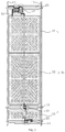
- FIG. 1 is a schematic diagram showing a flow chart of a driving method of a display panel provided in the present embodiment
- FIG. 1 is a schematic diagram showing a flow chart of a driving method of a display panel provided in the present embodiment, wherein the driving method is applicable on a situation that requires driving the display panel to carry out a plane display.
- the input device 930 can accept inputted digit or character information
- the output device 940 can include a display device such as a display panel.
Landscapes
- Engineering & Computer Science (AREA)
- Chemical & Material Sciences (AREA)
- Crystallography & Structural Chemistry (AREA)
- Physics & Mathematics (AREA)
- Computer Hardware Design (AREA)
- General Physics & Mathematics (AREA)
- Theoretical Computer Science (AREA)
- Control Of Indicators Other Than Cathode Ray Tubes (AREA)
- Liquid Crystal (AREA)
- Liquid Crystal Display Device Control (AREA)
Applications Claiming Priority (3)
| Application Number | Priority Date | Filing Date | Title |
|---|---|---|---|
| CN201710516338.6A CN107301847B (zh) | 2017-06-29 | 2017-06-29 | 一种显示面板的驱动方法、驱动装置及显示装置 |
| CN201710516338.6 | 2017-06-29 | ||
| PCT/CN2017/100257 WO2019000636A1 (zh) | 2017-06-29 | 2017-09-01 | 显示面板的驱动方法、驱动装置及显示装置 |
Publications (2)
| Publication Number | Publication Date |
|---|---|
| US20200372872A1 US20200372872A1 (en) | 2020-11-26 |
| US11004418B2 true US11004418B2 (en) | 2021-05-11 |
Family
ID=60136159
Family Applications (1)
| Application Number | Title | Priority Date | Filing Date |
|---|---|---|---|
| US16/622,646 Active US11004418B2 (en) | 2017-06-29 | 2017-09-01 | Display panel driving method, driving device, display device and non-transitory computer readable medium |
Country Status (3)
| Country | Link |
|---|---|
| US (1) | US11004418B2 (zh) |
| CN (1) | CN107301847B (zh) |
| WO (1) | WO2019000636A1 (zh) |
Families Citing this family (1)
| Publication number | Priority date | Publication date | Assignee | Title |
|---|---|---|---|---|
| CN114299892B (zh) * | 2021-12-24 | 2023-04-25 | 长沙惠科光电有限公司 | 像素结构、像素驱动方法、显示面板及显示设备 |
Citations (19)
| Publication number | Priority date | Publication date | Assignee | Title |
|---|---|---|---|---|
| US20070064182A1 (en) * | 2005-09-20 | 2007-03-22 | Au Optronics Corporation | Transflective liquid crystal display with multi-threshold harmonization |
| US20070153146A1 (en) * | 2005-05-03 | 2007-07-05 | Hannstar Display Corporation | Pixel Structure with Improved Viewing Angle |
| US20080246720A1 (en) * | 2007-04-03 | 2008-10-09 | Samsung Electronics Co., Ltd. | Display substrate and liquid crystal display having the same |
| CN101290411A (zh) | 2007-04-18 | 2008-10-22 | 奇美电子股份有限公司 | 液晶显示面板、液晶显示器及其驱动方法 |
| US20080284931A1 (en) * | 2007-05-17 | 2008-11-20 | Semiconductor Energy Laboratory Co., Ltd. | Liquid crystal display device |
| US20100220116A1 (en) * | 2009-02-27 | 2010-09-02 | Hannstar Display Corp. | Pixel structure and driving method thereof |
| US20110085105A1 (en) * | 2009-10-13 | 2011-04-14 | Park Kyung-Ho | Liquid crystal display and repairing method thereof |
| US20110170029A1 (en) * | 2007-05-17 | 2011-07-14 | Semiconductor Energy Laboratory Co., Ltd. | Liquid Crystal Display Device |
| US20110170031A1 (en) * | 2010-01-08 | 2011-07-14 | Samsung Electronics Co., Ltd. | Switching device of active display device and method of driving the switching device |
| US20110221988A1 (en) * | 2010-03-10 | 2011-09-15 | Samsung Electronics Co., Ltd. | Liquid crystal display |
| US20120026415A1 (en) * | 2009-03-05 | 2012-02-02 | Sharp Kabushiki Kaisha | Active matrix substrate, method for producing active matrix substrate, liquid crystal panel, method for producing liquid crystal panel, liquid crystal display device, liquid crystal display unit, and television receiver |
| US20120033148A1 (en) * | 2010-08-06 | 2012-02-09 | Samsung Electronics Co., Ltd. | Liquid crystal display |
| CN102436105A (zh) | 2011-10-20 | 2012-05-02 | 友达光电股份有限公司 | 液晶显示装置及其显示驱动方法 |
| CN102750899A (zh) | 2011-04-20 | 2012-10-24 | 乐金显示有限公司 | 图像显示装置及其驱动方法 |
| US20130249882A1 (en) * | 2012-03-26 | 2013-09-26 | Shenzhen China Star Optoelectronics Technology, Co., Ltd. | Liquid Crystal Display Device and Driving Method |
| CN103353698A (zh) | 2013-07-19 | 2013-10-16 | 深圳市华星光电技术有限公司 | 一种阵列基板及液晶显示面板 |
| US20140035968A1 (en) * | 2012-08-03 | 2014-02-06 | Au Optronics Corp. | Pixel circuit, pixel structure, 2d and 3d switchable display device and display driving method thereof |
| US9240152B2 (en) * | 2013-12-25 | 2016-01-19 | Shenzhen China Star Optoelectronics Technology Co., Ltd. | Array substrate and liquid crystal display panel and driving method thereof |
| US10593246B2 (en) * | 2017-11-08 | 2020-03-17 | E Ink Holdings Inc. | Pixel array substrate and display device |
Family Cites Families (10)
| Publication number | Priority date | Publication date | Assignee | Title |
|---|---|---|---|---|
| CN100507689C (zh) * | 2007-03-05 | 2009-07-01 | 友达光电股份有限公司 | 液晶显示器及其驱动方法 |
| CN100419818C (zh) * | 2007-04-23 | 2008-09-17 | 友达光电股份有限公司 | 液晶显示器及其驱动方法 |
| KR101538320B1 (ko) * | 2008-04-23 | 2015-07-23 | 삼성디스플레이 주식회사 | 표시 장치 |
| KR101015846B1 (ko) * | 2009-01-16 | 2011-02-23 | 삼성모바일디스플레이주식회사 | 전자 영상 기기 |
| WO2012063830A1 (ja) * | 2010-11-09 | 2012-05-18 | シャープ株式会社 | 液晶表示装置、表示装置およびゲート信号線駆動方法 |
| CN102707527B (zh) * | 2012-06-13 | 2015-07-15 | 深圳市华星光电技术有限公司 | 一种液晶显示面板及其阵列基板 |
| CN103257495B (zh) * | 2013-05-24 | 2015-11-25 | 深圳市华星光电技术有限公司 | 一种阵列基板及液晶显示面板 |
| CN104280965A (zh) * | 2014-10-29 | 2015-01-14 | 深圳市华星光电技术有限公司 | 显示面板及其中像素结构和驱动方法 |
| CN105046243B (zh) * | 2015-08-25 | 2019-12-20 | 业成光电(深圳)有限公司 | 显示装置 |
| CN105405424B (zh) * | 2015-12-16 | 2018-12-28 | 京东方科技集团股份有限公司 | 像素电路及其驱动方法、驱动电路、显示装置 |
-
2017
- 2017-06-29 CN CN201710516338.6A patent/CN107301847B/zh active Active
- 2017-09-01 WO PCT/CN2017/100257 patent/WO2019000636A1/zh active Application Filing
- 2017-09-01 US US16/622,646 patent/US11004418B2/en active Active
Patent Citations (19)
| Publication number | Priority date | Publication date | Assignee | Title |
|---|---|---|---|---|
| US20070153146A1 (en) * | 2005-05-03 | 2007-07-05 | Hannstar Display Corporation | Pixel Structure with Improved Viewing Angle |
| US20070064182A1 (en) * | 2005-09-20 | 2007-03-22 | Au Optronics Corporation | Transflective liquid crystal display with multi-threshold harmonization |
| US20080246720A1 (en) * | 2007-04-03 | 2008-10-09 | Samsung Electronics Co., Ltd. | Display substrate and liquid crystal display having the same |
| CN101290411A (zh) | 2007-04-18 | 2008-10-22 | 奇美电子股份有限公司 | 液晶显示面板、液晶显示器及其驱动方法 |
| US20080284931A1 (en) * | 2007-05-17 | 2008-11-20 | Semiconductor Energy Laboratory Co., Ltd. | Liquid crystal display device |
| US20110170029A1 (en) * | 2007-05-17 | 2011-07-14 | Semiconductor Energy Laboratory Co., Ltd. | Liquid Crystal Display Device |
| US20100220116A1 (en) * | 2009-02-27 | 2010-09-02 | Hannstar Display Corp. | Pixel structure and driving method thereof |
| US20120026415A1 (en) * | 2009-03-05 | 2012-02-02 | Sharp Kabushiki Kaisha | Active matrix substrate, method for producing active matrix substrate, liquid crystal panel, method for producing liquid crystal panel, liquid crystal display device, liquid crystal display unit, and television receiver |
| US20110085105A1 (en) * | 2009-10-13 | 2011-04-14 | Park Kyung-Ho | Liquid crystal display and repairing method thereof |
| US20110170031A1 (en) * | 2010-01-08 | 2011-07-14 | Samsung Electronics Co., Ltd. | Switching device of active display device and method of driving the switching device |
| US20110221988A1 (en) * | 2010-03-10 | 2011-09-15 | Samsung Electronics Co., Ltd. | Liquid crystal display |
| US20120033148A1 (en) * | 2010-08-06 | 2012-02-09 | Samsung Electronics Co., Ltd. | Liquid crystal display |
| CN102750899A (zh) | 2011-04-20 | 2012-10-24 | 乐金显示有限公司 | 图像显示装置及其驱动方法 |
| CN102436105A (zh) | 2011-10-20 | 2012-05-02 | 友达光电股份有限公司 | 液晶显示装置及其显示驱动方法 |
| US20130249882A1 (en) * | 2012-03-26 | 2013-09-26 | Shenzhen China Star Optoelectronics Technology, Co., Ltd. | Liquid Crystal Display Device and Driving Method |
| US20140035968A1 (en) * | 2012-08-03 | 2014-02-06 | Au Optronics Corp. | Pixel circuit, pixel structure, 2d and 3d switchable display device and display driving method thereof |
| CN103353698A (zh) | 2013-07-19 | 2013-10-16 | 深圳市华星光电技术有限公司 | 一种阵列基板及液晶显示面板 |
| US9240152B2 (en) * | 2013-12-25 | 2016-01-19 | Shenzhen China Star Optoelectronics Technology Co., Ltd. | Array substrate and liquid crystal display panel and driving method thereof |
| US10593246B2 (en) * | 2017-11-08 | 2020-03-17 | E Ink Holdings Inc. | Pixel array substrate and display device |
Also Published As
| Publication number | Publication date |
|---|---|
| US20200372872A1 (en) | 2020-11-26 |
| WO2019000636A1 (zh) | 2019-01-03 |
| CN107301847A (zh) | 2017-10-27 |
| CN107301847B (zh) | 2018-08-28 |
Similar Documents
| Publication | Publication Date | Title |
|---|---|---|
| US11355079B2 (en) | Array substrate, display panel, display device, and driving methods thereof | |
| US9501994B2 (en) | Liquid crystal display panel and driving method thereof | |
| US20190250442A1 (en) | Array substrate and manufacturing method thereof, display panel and driving method thereof, and electronic device | |
| US20160231605A1 (en) | Rgbw tft lcd having reduced horizontal crosstalk | |
| US9653028B2 (en) | Pixel structure | |
| CN102681224A (zh) | 液晶屏检测装置及方法 | |
| KR20090112087A (ko) | 표시 장치 | |
| CN101055386B (zh) | 图像显示系统 | |
| CN104795031A (zh) | 显示设备及用于驱动显示设备的方法 | |
| US10748500B2 (en) | Driving apparatus and method of display panel | |
| US20130335658A1 (en) | Pixel Architecture for Electronic Displays | |
| US10371978B2 (en) | Liquid crystal display device and electronic apparatus | |
| US10930240B2 (en) | Display panel driving method and driving device | |
| CN102292669B (zh) | 液晶显示装置 | |
| EP3715939A1 (en) | Pixel driving circuit and liquid crystal display panel | |
| US20160139462A1 (en) | Curved liquid crystal display | |
| US8432501B2 (en) | Liquid crystal display with improved side visibility | |
| US11004418B2 (en) | Display panel driving method, driving device, display device and non-transitory computer readable medium | |
| EP3637182A1 (en) | Liquid crystal display panel and device | |
| US20180356662A1 (en) | Liquid Crystal Display Panel and Apparatus | |
| US20210405483A1 (en) | Display panel and display device | |
| US11126048B2 (en) | Array substrate and display device | |
| US20190221583A1 (en) | Drive device and display device | |
| KR20160039763A (ko) | 액정 표시 장치 | |
| US10353236B2 (en) | Color film substrate and liquid crystal panel |
Legal Events
| Date | Code | Title | Description |
|---|---|---|---|
| AS | Assignment |
Owner name: HKC CORPORATION LIMITED, CHINA Free format text: ASSIGNMENT OF ASSIGNORS INTEREST;ASSIGNOR:CHEN, YU-JEN;REEL/FRAME:051278/0811 Effective date: 20180331 Owner name: CHONGQING HKC OPTOELECTRONICS TECHNOLOGY CO., LTD., CHINA Free format text: ASSIGNMENT OF ASSIGNORS INTEREST;ASSIGNOR:CHEN, YU-JEN;REEL/FRAME:051278/0811 Effective date: 20180331 |
|
| FEPP | Fee payment procedure |
Free format text: ENTITY STATUS SET TO UNDISCOUNTED (ORIGINAL EVENT CODE: BIG.); ENTITY STATUS OF PATENT OWNER: LARGE ENTITY |
|
| STPP | Information on status: patent application and granting procedure in general |
Free format text: NOTICE OF ALLOWANCE MAILED -- APPLICATION RECEIVED IN OFFICE OF PUBLICATIONS |
|
| STPP | Information on status: patent application and granting procedure in general |
Free format text: PUBLICATIONS -- ISSUE FEE PAYMENT VERIFIED |
|
| STCF | Information on status: patent grant |
Free format text: PATENTED CASE |