US10971237B2 - Semiconductor device - Google Patents
Semiconductor device Download PDFInfo
- Publication number
- US10971237B2 US10971237B2 US16/434,264 US201916434264A US10971237B2 US 10971237 B2 US10971237 B2 US 10971237B2 US 201916434264 A US201916434264 A US 201916434264A US 10971237 B2 US10971237 B2 US 10971237B2
- Authority
- US
- United States
- Prior art keywords
- input
- memory elements
- semiconductor device
- data
- terminal
- Prior art date
- Legal status (The legal status is an assumption and is not a legal conclusion. Google has not performed a legal analysis and makes no representation as to the accuracy of the status listed.)
- Expired - Fee Related, expires
Links
Images


Classifications
-
- G—PHYSICS
- G11—INFORMATION STORAGE
- G11C—STATIC STORES
- G11C16/00—Erasable programmable read-only memories
- G11C16/02—Erasable programmable read-only memories electrically programmable
- G11C16/06—Auxiliary circuits, e.g. for writing into memory
- G11C16/10—Programming or data input circuits
- G11C16/20—Initialising; Data preset; Chip identification
-
- G—PHYSICS
- G11—INFORMATION STORAGE
- G11C—STATIC STORES
- G11C16/00—Erasable programmable read-only memories
- G11C16/02—Erasable programmable read-only memories electrically programmable
- G11C16/06—Auxiliary circuits, e.g. for writing into memory
- G11C16/26—Sensing or reading circuits; Data output circuits
-
- G—PHYSICS
- G06—COMPUTING OR CALCULATING; COUNTING
- G06F—ELECTRIC DIGITAL DATA PROCESSING
- G06F13/00—Interconnection of, or transfer of information or other signals between, memories, input/output devices or central processing units
- G06F13/14—Handling requests for interconnection or transfer
- G06F13/16—Handling requests for interconnection or transfer for access to memory bus
- G06F13/1668—Details of memory controller
-
- G—PHYSICS
- G06—COMPUTING OR CALCULATING; COUNTING
- G06F—ELECTRIC DIGITAL DATA PROCESSING
- G06F13/00—Interconnection of, or transfer of information or other signals between, memories, input/output devices or central processing units
- G06F13/38—Information transfer, e.g. on bus
- G06F13/382—Information transfer, e.g. on bus using universal interface adapter
- G06F13/385—Information transfer, e.g. on bus using universal interface adapter for adaptation of a particular data processing system to different peripheral devices
-
- G—PHYSICS
- G06—COMPUTING OR CALCULATING; COUNTING
- G06F—ELECTRIC DIGITAL DATA PROCESSING
- G06F13/00—Interconnection of, or transfer of information or other signals between, memories, input/output devices or central processing units
- G06F13/38—Information transfer, e.g. on bus
- G06F13/42—Bus transfer protocol, e.g. handshake; Synchronisation
- G06F13/4204—Bus transfer protocol, e.g. handshake; Synchronisation on a parallel bus
-
- G—PHYSICS
- G06—COMPUTING OR CALCULATING; COUNTING
- G06F—ELECTRIC DIGITAL DATA PROCESSING
- G06F13/00—Interconnection of, or transfer of information or other signals between, memories, input/output devices or central processing units
- G06F13/38—Information transfer, e.g. on bus
- G06F13/42—Bus transfer protocol, e.g. handshake; Synchronisation
- G06F13/4282—Bus transfer protocol, e.g. handshake; Synchronisation on a serial bus, e.g. I2C bus, SPI bus
-
- G—PHYSICS
- G06—COMPUTING OR CALCULATING; COUNTING
- G06K—GRAPHICAL DATA READING; PRESENTATION OF DATA; RECORD CARRIERS; HANDLING RECORD CARRIERS
- G06K19/00—Record carriers for use with machines and with at least a part designed to carry digital markings
- G06K19/06—Record carriers for use with machines and with at least a part designed to carry digital markings characterised by the kind of the digital marking, e.g. shape, nature, code
- G06K19/067—Record carriers with conductive marks, printed circuits or semiconductor circuit elements, e.g. credit or identity cards also with resonating or responding marks without active components
- G06K19/07—Record carriers with conductive marks, printed circuits or semiconductor circuit elements, e.g. credit or identity cards also with resonating or responding marks without active components with integrated circuit chips
- G06K19/073—Special arrangements for circuits, e.g. for protecting identification code in memory
-
- G—PHYSICS
- G11—INFORMATION STORAGE
- G11C—STATIC STORES
- G11C16/00—Erasable programmable read-only memories
- G11C16/02—Erasable programmable read-only memories electrically programmable
- G11C16/06—Auxiliary circuits, e.g. for writing into memory
- G11C16/10—Programming or data input circuits
- G11C16/102—External programming circuits, e.g. EPROM programmers; In-circuit programming or reprogramming; EPROM emulators
- G11C16/105—Circuits or methods for updating contents of nonvolatile memory, especially with 'security' features to ensure reliable replacement, i.e. preventing that old data is lost before new data is reliably written
-
- G—PHYSICS
- G11—INFORMATION STORAGE
- G11C—STATIC STORES
- G11C16/00—Erasable programmable read-only memories
- G11C16/02—Erasable programmable read-only memories electrically programmable
- G11C16/06—Auxiliary circuits, e.g. for writing into memory
- G11C16/22—Safety or protection circuits preventing unauthorised or accidental access to memory cells
-
- G—PHYSICS
- G11—INFORMATION STORAGE
- G11C—STATIC STORES
- G11C17/00—Read-only memories programmable only once; Semi-permanent stores, e.g. manually-replaceable information cards
- G11C17/06—Read-only memories programmable only once; Semi-permanent stores, e.g. manually-replaceable information cards using diode elements
-
- G—PHYSICS
- G11—INFORMATION STORAGE
- G11C—STATIC STORES
- G11C17/00—Read-only memories programmable only once; Semi-permanent stores, e.g. manually-replaceable information cards
- G11C17/08—Read-only memories programmable only once; Semi-permanent stores, e.g. manually-replaceable information cards using semiconductor devices, e.g. bipolar elements
-
- G—PHYSICS
- G11—INFORMATION STORAGE
- G11C—STATIC STORES
- G11C5/00—Details of stores covered by group G11C11/00
- G11C5/06—Arrangements for interconnecting storage elements electrically, e.g. by wiring
- G11C5/066—Means for reducing external access-lines for a semiconductor memory clip, e.g. by multiplexing at least address and data signals
-
- G—PHYSICS
- G11—INFORMATION STORAGE
- G11C—STATIC STORES
- G11C7/00—Arrangements for writing information into, or reading information out from, a digital store
- G11C7/10—Input/output [I/O] data interface arrangements, e.g. I/O data control circuits, I/O data buffers
- G11C7/1015—Read-write modes for single port memories, i.e. having either a random port or a serial port
- G11C7/1036—Read-write modes for single port memories, i.e. having either a random port or a serial port using data shift registers
-
- G—PHYSICS
- G11—INFORMATION STORAGE
- G11C—STATIC STORES
- G11C7/00—Arrangements for writing information into, or reading information out from, a digital store
- G11C7/10—Input/output [I/O] data interface arrangements, e.g. I/O data control circuits, I/O data buffers
- G11C7/1015—Read-write modes for single port memories, i.e. having either a random port or a serial port
- G11C7/1042—Read-write modes for single port memories, i.e. having either a random port or a serial port using interleaving techniques, i.e. read-write of one part of the memory while preparing another part
-
- G—PHYSICS
- G11—INFORMATION STORAGE
- G11C—STATIC STORES
- G11C7/00—Arrangements for writing information into, or reading information out from, a digital store
- G11C7/10—Input/output [I/O] data interface arrangements, e.g. I/O data control circuits, I/O data buffers
- G11C7/1078—Data input circuits, e.g. write amplifiers, data input buffers, data input registers, data input level conversion circuits
-
- G—PHYSICS
- G06—COMPUTING OR CALCULATING; COUNTING
- G06F—ELECTRIC DIGITAL DATA PROCESSING
- G06F2213/00—Indexing scheme relating to interconnection of, or transfer of information or other signals between, memories, input/output devices or central processing units
- G06F2213/0002—Serial port, e.g. RS232C
-
- G—PHYSICS
- G06—COMPUTING OR CALCULATING; COUNTING
- G06F—ELECTRIC DIGITAL DATA PROCESSING
- G06F2213/00—Indexing scheme relating to interconnection of, or transfer of information or other signals between, memories, input/output devices or central processing units
- G06F2213/0004—Parallel ports, e.g. centronics
-
- G—PHYSICS
- G06—COMPUTING OR CALCULATING; COUNTING
- G06F—ELECTRIC DIGITAL DATA PROCESSING
- G06F2213/00—Indexing scheme relating to interconnection of, or transfer of information or other signals between, memories, input/output devices or central processing units
- G06F2213/38—Universal adapter
- G06F2213/3852—Converter between protocols
-
- G—PHYSICS
- G11—INFORMATION STORAGE
- G11C—STATIC STORES
- G11C19/00—Digital stores in which the information is moved stepwise, e.g. shift registers
-
- G—PHYSICS
- G11—INFORMATION STORAGE
- G11C—STATIC STORES
- G11C2207/00—Indexing scheme relating to arrangements for writing information into, or reading information out from, a digital store
- G11C2207/10—Aspects relating to interfaces of memory device to external buses
- G11C2207/107—Serial-parallel conversion of data or prefetch
-
- G—PHYSICS
- G11—INFORMATION STORAGE
- G11C—STATIC STORES
- G11C7/00—Arrangements for writing information into, or reading information out from, a digital store
- G11C7/10—Input/output [I/O] data interface arrangements, e.g. I/O data control circuits, I/O data buffers
- G11C7/1006—Data managing, e.g. manipulating data before writing or reading out, data bus switches or control circuits therefor
- G11C7/1012—Data reordering during input/output, e.g. crossbars, layers of multiplexers, shifting or rotating
-
- G—PHYSICS
- G11—INFORMATION STORAGE
- G11C—STATIC STORES
- G11C7/00—Arrangements for writing information into, or reading information out from, a digital store
- G11C7/10—Input/output [I/O] data interface arrangements, e.g. I/O data control circuits, I/O data buffers
- G11C7/1015—Read-write modes for single port memories, i.e. having either a random port or a serial port
- G11C7/1045—Read-write mode select circuits
-
- G—PHYSICS
- G11—INFORMATION STORAGE
- G11C—STATIC STORES
- G11C7/00—Arrangements for writing information into, or reading information out from, a digital store
- G11C7/10—Input/output [I/O] data interface arrangements, e.g. I/O data control circuits, I/O data buffers
- G11C7/1078—Data input circuits, e.g. write amplifiers, data input buffers, data input registers, data input level conversion circuits
- G11C7/109—Control signal input circuits
Definitions
- the present invention relates to a semiconductor device, and particularly to a semiconductor device that outputs fixed data in which the data value is fixed.
- a semiconductor device such as a semiconductor IC (integrated circuit) chip can be used to store fixed data in which a data value, such as an identifier (also referred to below as ID), is fixed.
- ID a data value
- the ID may be read out from the semiconductor device for various purposes and at various times.
- IDs examples include chip IDs (unique IDs), device IDs (product IDs), device address codes (slave addresses), and the like.
- Chip IDs are unique IDs for distinguishing individual semiconductor IC chips, which are mass produced, and the IDs indicate the number of the lot in which the chip was manufactured, the number of the wafer from which the chip was cut out, the position of the chip on the wafer (chip position), the manufacturing date, or the like (see Japanese Patent Application Laid-Open Publication No. 2008-10549, for example).
- Device IDs are IDs assigned to each type of product, and unless there are revisions all mass produced semiconductor IC chips that are the same product are assigned the same ID (see Japanese Translation of PCT International Application Publication No. 2010-506284, page 14, table 6, for example).
- Device address codes are IDs used in order to identify each semiconductor IC chip when constructing a system for enabling a plurality of semiconductor IC chips to communicate with each other through a bus (communication path). Where at least one of the plurality of semiconductor IC chips is a master device and other semiconductor IC chips are slave devices, the device address code is used for the master device to identify and individually control each of the slave devices.
- Japanese Translation of PCT International Application Publication No. 2010-506284 proposes a flash memory control interface in which a memory controller functioning as a master device individually controls a plurality of flash memories functioning as slave devices.
- IDs generated by the memory controller itself are written to the reserved memory unit of each flash memory to set a unique device address code for each flash memory.
- Japanese Patent Application Laid-Open Publication No. 2008-10549 discloses a semiconductor device including a plurality of fuse elements having states (connection/disconnection) respectively corresponding to the plurality of bits indicating the ID in order to store various IDs as described above in the semiconductor IC chip, for example.
- the semiconductor device according to embodiments of the invention has a function of outputting the IDs stored therein to an external unit through an interface unit.
- a configuration for a flash memory is known in which information data pieces read from the memory cell array thereof are outputted to an external unit in a serial signal format through an SPI (serial-parallel interface) bus, for example.
- SPI serial-parallel interface
- Such a flash memory is provided with a parallel/serial conversion circuit (hereinafter, referred to as P/S conversion circuit) that converts the parallel format information data pieces (hereinafter referred to as read data pieces) read from the memory cell array to serial format.
- the P/S conversion circuit includes a shift register constituted of a plurality of flip-flops (hereinafter referred to as FFs) that are in a cascade arrangement. Additionally, in the P/S conversion circuit, a so-called 2-to-1 selector of a 2-input selection-type that causes bits of a read data piece to be acquired by the FFs constituting the shift register is provided between FFs that are connected to each other. The 2-to-1 selector selects either one of 1 bit of the read data piece or 1 bit outputted from the previous stage FF, and supplies the bit to the next stage FF.
- FFs flip-flops
- the read data piece is acquired by the shift register if the 2-to-1 selector selects the 1 bit within the read data piece.
- the 2-to-1 selector selects the 1 bit outputted from the previous stage FF, then the read data piece acquired by the shift register is shifted 1 bit at a time and transmitted to the SPI bus in order from the last stage FF.
- the flash memory be provided with the function of being able to output through the SPI bus not only the read data piece but also a plurality of data pieces representing the state of the flash memory, the ID, and the like.
- a configuration is adopted in which the fixed data as the ID is stored in advance in a fuse element, a non-volatile memory, or the like, and when necessary, a plurality of bits indicating this ID are read, and acquired by the P/S conversion circuit in parallel format, for example.
- one possible configuration is to adopt an N-input selector (N being an integer of 3 or greater) that causes the shift register to selectively acquire the plurality of information data pieces including the state of the device as well as fixed data such as the ID, instead of the 2-to-1 selector provided between individual FFs of the P/S conversion circuit.
- An object of the present invention is to provide a semiconductor device by which it is possible to set fixed data without resulting in a decrease in processing speed or an increase in power consumption.
- a semiconductor device is a semiconductor device that uses fixed data constituted of a plurality of bits, the semiconductor device including: a plurality of memory elements that correspond, respectively, to the plurality of bits of the fixed data, and that acquire, store, and output the value of each bit received at an input terminal of each of the memory elements according to a timing signal; and an initialization control unit that feeds, to the plurality of memory elements, an initialization signal upon receipt of a fixed data setting signal, wherein each of the plurality of memory elements is initialized to a state of storing a corresponding value represented by a bit of the fixed data according to the initialization signal.
- the plurality of memory elements that correspond, respectively, to the plurality of bits of the fixed data, and that acquire, store, and output the value of each bit received at an input terminal of each of the memory elements according to a timing signal, are initialized as follows according to a setting signal for the fixed data. That is, each of the plurality of memory elements is initialized to a state of storing a corresponding value represented by a bit of the fixed data according to the initialization signal.
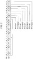
- FIG. 1 is a block diagram showing the configuration of a memory unit 100 included in a semiconductor device according to the present invention.
- FIG. 2 is a data format diagram showing one example of a device ID [0:23].
- FIG. 3 is a block diagram showing one example of an internal configuration of a P/S conversion circuit 125 .
- FIG. 4 is a block diagram showing an example of an internal configuration of each 8-input selector SL 0 to SL 7 .
- FIG. 5 shows an example of the relationship between the selection signal SED and operation modes.
- FIG. 6 is a time chart showing an example of an internal operation in the P/S conversion circuit 125 .
- FIG. 7 is a block diagram showing a modification example of an internal configuration of the P/S conversion circuit 125 .
- FIG. 8 is a block diagram showing another modification example of an internal configuration of the P/S conversion circuit 125 .
- FIG. 1 is a block diagram showing the configuration of a memory unit 100 included in a semiconductor device according to the present invention.
- the memory unit 100 is a NAND flash memory, for example, and includes a memory cell array 10 , an array controller 11 , and a memory controller 12 .
- the memory cell array 10 is constituted of a plurality of banks, each of which includes a plurality of memory cells.
- the array controller 11 generates various voltages for writing data, reading data, or deleting data according to an address supplied from the memory controller 12 and a read command, write command, or delete command, and supplies the voltages to the memory cell group in the memory cell array 10 corresponding to the address.
- the array controller 11 detects the current sent from the memory cell group in the memory cell array 10 and determines the value of the read data on the basis of the detected current. Then, the array controller 11 generates the determined read data as read data MEM[0:7] indicated with 8 bits, for example, and supplies the read data to the memory controller 12 .
- the memory controller 12 includes various registers such as a status register 121 , a configuration register 122 , a bank address register 123 , and a sector protection register 124 , as well as an ID storage unit 130 . Additionally, the memory controller 12 includes a P/S (parallel/serial) conversion circuit 125 and an output buffer 126 .
- P/S parallel/serial
- the status register 121 stores status data SR[0:7] that indicates the current state of the memory unit 100 in 8 bits.
- the configuration register 122 stores configuration data CFG[0:7] that indicates setting information for the memory control method performed by the memory controller 12 in 8 bits.
- the bank address register 123 stores a bank address BA[0:7] that indicates the position of each of the banks included in the memory cell array 10 in 8 bits.
- the sector protection register 124 stores sector protection data SP[0:7] indicating sectors to be excluded from data writing or deletion in each bank included in the memory cell array 10 in 8 bits.
- the ID storage unit 130 stores an ID [0:15] included within the device ID [0:23] that indicates in 24 bits specific information of the product type of the host device. As will be described later, unlike typical examples, in the present invention, the remaining ID [16:23] is stored in a distributed manner in the P/S conversion circuit 125 .
- the memory controller 12 stores identification information, which may include chip IDs, device IDs, device address codes, or any other type of identification information as an ID, and a portion of the ID is stored in the ID storage unit 130 while a remainder of the ID is stored in a distributed manner in the P/S conversion circuit 125 .
- FIG. 2 is a data format diagram showing one example of the device ID [0:23].
- the ID storage unit 130 shown in FIG. 1 stores an ID [0:7] constituted of a 0th bit to a 7th bit and an ID [8:15] constituted of an 8th bit to a 15th bit, within the device ID [0:23] shown in FIG. 2 , and supplies the ID [0:7] and the ID [8:15] to the P/S conversion circuit 125 .
- the P/S conversion circuit 125 receives the above-mentioned read data MEM[0:7], the status data SR[0:7], the configuration data CFG[0:7], the bank address BA[0:7], the sector protection data SP[0:7], and the device ID [0:15].
- the P/S conversion circuit 125 first selects one group's worth of data pieces, among the above-mentioned six groups of information data pieces including the MEM[0:7], the SR[0:7], the CFG[0:7], the BA[0:7], the SP[0:7], and the ID[0:15], to be subjected to parallel/serial conversion. Next, the P/S conversion circuit 125 converts the selected one group's worth of data pieces into a serial data signal SIO for each bit, and supplies the serial data signal to the output buffer 126 .
- the output buffer 126 sends the serial data signal SIO to a serial bus SBS through an output terminal SO according to an output enable signal EN.
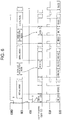
- FIG. 3 is a circuit diagram showing an example of an internal configuration of the P/S conversion circuit 125 .
- the P/S conversion circuit 125 includes a shift register including flip-flops FF 0 to FF 7 , 8-input selectors SL 0 to SL 7 , and an AND gate AN.
- Each of the 8-input selectors SL 0 to SL 7 has eight input terminals (a, b, c, d, e, f, g, h). Each of the 8-input selectors SL 0 to SL 7 selects a data bit received by one input terminal selected according to a selection signal SED, among the input terminals a to h, and outputs the data bit to an output terminal Y.
- the selection signal may be a control signal provided by a memory control device or processor (not shown), for example, or it may be provided from the array controller 11 .
- FIG. 4 is a circuit diagram showing one example of an internal configuration of each 8-input selector SL 0 to SL 7 .
- each 8-input selector SL 0 to SL 7 has a 2-input selector 41 and 4-input selectors 42 and 43 .
- the selection signal SED is constituted of five selection bits (SELA[0], SELA[1], SELB[0], SELB[1], SELC) as shown in FIG. 4 .
- the 2-input selector 41 selects the data bit received by the input terminal a or the data bit received by the input terminal b on the basis of the binary (logic level of 0 or 1) value of the selection bit SELC, and supplies this data bit as a selection data bit r to the 4-input selector 42 in the next stage.
- the 4-input selector 42 selects one of the selection data bit r, the data bit received by the input terminal c, the data bit received by the input terminal d, and the data bit received by the input terminal e on the basis of the binary values of the selection bits SELB[0] and SELB[1].
- the 4-input selector 42 supplies the one selected data bit as a selection data bit t to the 4-input selector 43 in the next stage.
- the 4-input selector 43 selects one of the selection data bit t, the data bit received by the input terminal f, the data bit received by the input terminal g, and the data bit received by the input terminal h on the basis of the binary values of the selection bits SELA[0] and SELA[1].
- the 4-input selector 43 outputs the one selected data bit as a selection data bit through the output terminal Y.
- the input terminals a of the 8-input selectors SL 0 to SL 7 respectively receive as data bits the device ID [8], ID[9], ID[10], ID[11], ID[12], ID[13], ID[14], and ID[15], as shown in FIG. 3 .
- the input terminals b of the 8-input selectors SL 0 to SL 7 respectively receive as data bits the device ID [0], ID[1], ID[2], ID[3], ID[4], ID[5], ID[6], and ID[7], as shown in FIG. 3 .
- the input terminals c of the 8-input selectors SL 0 to SL 7 respectively receive as data bits the bank addresses BA[0], BA[1], BA[2], BA[3], BA[4], BA[5], BA[6], and BA[7], as shown in FIG. 3 .
- the input terminals d of the 8-input selectors SL 0 to SL 7 respectively receive as data bits the sector protection data SP[0], SP[1], SP[2], SP[3], SP[4], SP[5], SP[6], and SP[7], as shown in FIG. 3 .
- the input terminals e of the 8-input selectors SL 0 to SL 7 respectively receive as data bits the configuration data CFG[0], CFG[1], CFG[2], CFG[3], CFG[4], CFG[5], CFG[6], and CFG[7], as shown in FIG. 3 .
- the input terminals f of the 8-input selectors SL 0 to SL 7 respectively receive as data bits the read data MEM[0], MEM[1], MEM[2], MEM[3], MEM[4], MEM[5], MEM[6], and MEM[7], as shown in FIG. 3 .
- the input terminals g of the 8-input selectors SL 0 to SL 7 respectively receive as data bits the status data SR[0], SR[1], SR[2], SR[3], SR[4], SR[5], SR[6], and SR[7], as shown in FIG. 3 .
- the 8-input selector SL 0 selects one of the above-mentioned ID[8], ID[0], BA[0], SP[0], CFG[0], MEM[0], and SR[0] according to the selection signal SED (SELA[0], SELA[1], SELB[0], SELB[1], SELC).
- the 8-input selector SL 0 supplies to the input terminal D of the flip-flop FF 0 , the selected ID[8], ID[0], BA[0], SP[0], CFG[0], MEM[0], or SR[0] as a data bit D 0 .
- the input terminal h of the 8-input selector SL 0 is unused, and thus, is supplied ground potential.
- the flip-flop FF 0 acquires the data bit D 0 at the rising edge of a clock signal CLK, which is a timing signal, and supplies an output signal Q[0] of the flip-flop FF 0 to the input terminal h of the 8-input selector SL 1 .
- the 8-input selector SL 1 selects any of the above-mentioned ID[9], ID[1], BA[1], SP[1], CFG[1], MEM[1], SR[1], and the data bit Q[0] supplied from the flip-flop FF 0 according to the selection signal SED.
- the 8-input selector SL 1 supplies to the input terminal D of the flip-flop FF 1 , the selected ID[9], ID[1], BA[1], SP[1], CFG[1], MEM[1], SR[1], or Q[0] as a data bit D 1 .
- the flip-flop FF 1 acquires the data bit D 1 at the rising edge of the clock signal CLK, and supplies an output signal Q[1] of the flip-flop FF 1 to the input terminal h of the 8-input selector SL 2 .
- the 8-input selector SLw (where w is an integer of 2-7) selects any of the above-mentioned ID[w+8], ID[w], BA[w], SP[w], CFG[w], MEM[w], SR[w], and the data bit Q[w ⁇ 1] supplied from the flip-flop FF[w ⁇ 1] according to the selection signal SED.
- the 8-input selector SLw supplies to the input terminal D of the flip-flop FFw, the selected ID[w+8], ID[w], BA[w], SP[w], CFG[w], MEM[w], SR[w], or the data bit supplied from the flip-flop FF[w ⁇ 1] as a data bit Dw.
- the flip-flop FFw acquires and retains the data bit Dw at the rising edge of the clock signal CLK, and (excluding FF 7 ) supplies an output signal Q[w] of the flip-flop FFw to the input terminal h of the 8-input selector SLw+1.
- the flip-flop FF 7 which is the last stage of the shift register, acquires and retains the data bit D 7 at the rising edge of the clock signal CLK, and outputs the data bit as the data bit Q[7].
- the P/S conversion circuit 125 outputs the data bit Q[7] outputted from the flip-flop FF 7 as the serial data signal SIO.
- the flip-flops FF 0 to FF 7 each have a set terminal S, whereas the flip-flops FF 1 , FF 3 , FF 5 , and FF 7 have a reset terminal R.
- the flip-flops FF 0 to FF 7 receive the initialization signals INI at times that are not synchronized to the clock signal CLK, and are initialized to a set state or a reset state as described above according to the initialization signal INI.
- the AND gate AN receives a power on reset signal POR and an ID setting signal IDS.
- the power on reset signal POR stays at a logic level of 0, which prompts initialization of flip-flops for only a prescribed period, and then stays at a logic level of 1 when the memory unit 100 is powered on.
- the ID setting signal IDS is a signal that is not synchronized to the clock signal CLK, and that corresponds to the ID read command signal supplied from a source external to the memory unit 100 , for example. If the ID setting signal IDS is at a logic level of 0, for example, then among the device ID [0:23] shown in FIG. 2 , the values (logic level of 0 or 1) of the ID [16:23] are set to the flip-flops FF 0 to FF 7 .
- the AND gate AN If either one of the power on reset signal POR and the ID setting signal IDS is at a logic level of 0, then the AND gate AN generates an initialization signal at a logic level of 0, which prompts initialization.
- the AND gate AN supplies the initialization signal INI to the set terminals S of the flip-flops FF 0 , FF 2 , FF 4 , and FF 6 , and to the reset terminals R of the flip-flops FF 1 , FF 3 , FF 5 , and FF 7 .
- the P/S conversion circuit 125 operates in an operation mode set according to the selection signal SED.
- FIG. 5 shows an example of the relationship between the selection signal SED (SELA[1], SELA[0], SELB[1], SELB[0], SELC) and operation modes set according to the selection signal SED.
- the 8-input selectors SL 0 to SL 7 supply to the input terminals D of the flip-flops FF 0 to FF 7 the read data MEM[0:7] received by the input terminals f.
- the pieces of read data MEM[0:7] read from the memory cell array 10 are acquired by the shift register (FF 0 -FF 7 ) in a parallel manner.
- each flip-flop of the shift register causes the acquired 8-bit read data MEM[0:7] to be shifted by 1 bit each by the next stage flip-flop in synchronization with the rising edge of the clock signal CLK, and outputs the resultant data as the serial data signal SIO from the last stage flip-flop FF 7 .
- the P/S conversion circuit 125 successively outputs 1 bit at a time the read data MEM[0:7] outputted from the array controller 11 as the serial data signal SIO generated by converting the read data to a serial format.
- the P/S conversion circuit 125 when BA acquisition mode and serial mode are successively selected according to the selection signal SED, the P/S conversion circuit 125 successively outputs 1 bit at a time the bank address BA[0:7] stored in the bank address register 123 as the serial data signal SIO generated by converting the bank address to a serial format.
- the P/S conversion circuit 125 when SP acquisition mode and serial mode are successively selected according to the selection signal SED, the P/S conversion circuit 125 successively outputs 1 bit at a time the sector protection data SP[0:7] stored in the array controller 124 as the serial data signal SIO generated by converting the sector protection data to a serial format.
- the P/S conversion circuit 125 when CFG acquisition mode and serial mode are successively selected according to the selection signal SED, the P/S conversion circuit 125 successively outputs 1 bit at a time the configuration data CFG[0:7] stored in the configuration register 122 as the serial data signal SIO generated by converting the configuration data to a serial format.
- the P/S conversion circuit 125 when SR acquisition mode and serial mode are successively selected according to the selection signal SED, the P/S conversion circuit 125 successively outputs 1 bit at a time the status data SR[0:7] stored in the status register 121 as the serial data signal SIO generated by converting the status data to a serial format.
- the P/S conversion circuit 125 converts the 24-bit device ID [0:23] as fixed data to a serial format by the following method and outputs the device ID.
- FIG. 6 is an example of a timing chart for an internal operation performed when the P/S conversion circuit 125 converts the device ID [0:23] to a serial format and outputs the device ID as the serial data signal SIO.
- the P/S conversion circuit 125 has inputted thereto the ID setting signal IDS at a logic level of 0, which causes the device ID to be set as the fixed data, according to the ID read command signal IDRD.
- the flip-flops FF 0 , FF 2 , FF 4 , and FF 6 shown in FIG. 3 are initialized to the set state, and the flip-flops FF 1 , FF 3 , FF 5 , and FF 7 are initialized to the reset state.
- the 8-bit device ID [16:23] corresponding to the 16th to 23rd bits of the device ID shown in FIG. 2 is acquired by the flip-flops FF 0 to FF 7 .
- the serial mode continues to be set according to the selection signal SED.
- the shift register (FF 0 -FF 7 ) outputs 1 bit at a time the acquired device ID [16:23] in the order of the ID[23], ID[22], ID[21], ID[20], ID[19], ID[18], ID[17], and ID[16] as shown in FIG. 6 , in synchronization with the rising edge of the clock signal CLK, as the serial data signal SIO.
- the ID[8:15] acquisition mode continues to be designated according to the selection signal SED.
- the 8-input selectors SL 0 to SL 7 supply to the input terminals D 0 to D 7 of the flip-flops FF 0 to FF 7 the device ID received by the input terminals a, that is, the device ID [8:15] corresponding to the 8th to 15th bits of the device ID shown in FIG. 2 .
- the device ID [8:15] stored in the ID storage unit 130 is acquired by the shift register (FF 0 -FF 7 ) at the rising edge of the clock signal CLK following the rising edge when outputting the device ID [16] as shown in FIG. 6 .
- the serial mode is set according to the selection signal SED as shown in FIG. 6 .
- the 8-input selectors SL 1 to SL 7 supply to the input terminals D 1 to D 7 of the next stage flip-flops FF 1 to FF 7 the data bits Q[0:6] outputted from the previous stage flip-flops FF 0 to FF 6 received by the input terminals h.
- the shift register outputs 1 bit at a time the 8-bit device ID [8:15] in the order of the ID[15], ID[14], ID[13], ID[12], ID[11], ID[10], ID[9], and ID[8] as shown in FIG. 6 , in synchronization with the rising edge of the clock signal CLK, as the serial data signal SIO.
- the ID[0:7] acquisition mode continues to be designated according to the selection signal SED.
- the 8-input selectors SL 0 to SL 7 supply to the input terminals D 0 to D 7 of the flip-flops FF 0 to FF 7 the device ID received by the input terminals b, that is, the device ID [0:7] corresponding to the 0th to 7th bits of the device ID shown in FIG. 2 .
- the device ID [0:7] stored in the ID storage unit 130 is acquired by the shift register (FF 0 -FF 7 ) at the rising edge of the clock signal CLK following the rising edge when outputting the device ID [8] as shown in FIG. 6 .
- the serial mode is set according to the selection signal SED as shown in FIG. 6 .
- the 8-input selectors SL 1 to SL 7 supply to the input terminals D 1 to D 7 of the next stage flip-flops FF 1 to FF 7 the data bits Q[0:6] outputted from the previous stage flip-flops FF 0 to FF 6 received by the input terminals h.
- the shift register outputs 1 bit at a time the 8-bit device ID [0:7] in the order of the ID[7], ID[6], ID[5], ID[4], ID[3], ID[2], ID[1], and ID[0] as shown in FIG. 6 , in synchronization with the rising edge of the clock signal CLK, as the serial data signal SIO.
- the P/S conversion circuit 125 in converting the device ID [0:23] as fixed data to a serial format and outputting it, first, signals are supplied through the selectors (SL 0 to SL 7 ) to the input terminals D 0 to D 7 of the flip-flops FF 0 to FF 7 for the device ID [0:7] or [8:15]. As a result, the flip-flops FF 0 to FF 7 acquire the values of the 8-bit device ID [0:7] or [8:15] in a parallel manner at the rising edge of the clock signal CLK.
- the shift register constituted of the flip-flops FF 0 to FF 7 outputs 1 bit at a time the acquired 8-bit device ID [0:7] or [8:15] successively in synchronization with the rising edge of the clock signal CLK, as the serial data signal SIO.
- the device ID [16:23] is acquired by and stored in the flip-flops FF 0 to FF 7 without passing through the selectors (SL 0 to SL 7 ) by initialization of the reset terminal R or the set terminal S of the flip-flops FF 0 to FF 7 .
- the shift register (FF 0 to FF 7 ) outputs 1 bit at a time the set 8-bit device ID [16:23] successively in synchronization with the rising edge of the clock signal CLK, as the serial data signal SIO.
- the 8-bit device ID [16:23] for which there is no margin for setup time for the flip-flops to read the ID read command signal IDRD shown in FIG. 6 immediately after receipt thereof, is acquired by the shift register (FF 0 to FF 7 ) by asynchronous initialization without depending on the clock signal CLK.
- the shift register (FF 0 to FF 7 ) acquires the device ID [16:23]
- the device ID [8:15] fed to the input terminal a would pass through three stages of selectors ( 41 , 42 , 43 ) and be fed to the input terminal D of each of the flip-flops FF 0 to FF 7 .
- the device ID [0:7] fed to the input terminal b would pass through three stages of selectors ( 41 , 42 , 43 ) and be fed to the input terminal D of each of the flip-flops FF 0 to FF 7 .
- selection of serial mode by the selection signal SED depends only on the selection bit SELA [0:1], and the selection bits SELB[0:1] and SELC are not relevant.
- the SELB [0:1] and the SELC are both set to a logic level of 0 as shown in FIG. 5 .
- the SELB [0:1] is set to a logic level of 0 and the SELC is set to a logic level of 1 as shown in FIG. 5 .
- the delay time at each of the 8-input selectors SL 0 to SL 7 during acquisition of the device ID [0:7] or [8:15] is in reality only for one stage of the 4-input selector 43 shown in FIG. 4 .
- the device ID [16:23] among the device ID [0:23] is acquired by the shift register without passing through the 8-input selectors (SL 0 -SL 7 ).
- the P/S conversion circuit 125 it is possible to selectively output a plurality of information data pieces (ID, BA, SP, CFG, MEM, SR) including a fixed data piece (ID) in a serial manner without resulting in decreased processing speed, increased power consumption, or increased chip area.
- the 16th to 23rd bits of the device ID [0:23] correspond to the flip-flops FF 0 to FF 7 in the following way.
- flip-flops corresponding to the bits indicating a logic level of 0 (first value) among the 16th to 23rd bits of the device ID [0:23] have reset terminals, and flip-flops corresponding to bits having a logic level of 1 (second value) have set terminals.
- the flip-flops FF 0 to FF 7 may each have both a set terminal and a reset terminal.
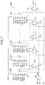
- FIG. 7 is a circuit diagram showing a P/S conversion circuit 125 A as a modification example of the P/S conversion circuit 125 that was made taking into consideration the aforementioned points.
- the same configuration is used as that of FIG. 3 aside from the flip-flops FF 0 to FF 7 .
- the reset terminals R of the flip-flops FF 0 , FF 2 , FF 4 , and FF 6 , and the set terminals S of the flip-flops FF 1 , FF 3 , FF 5 , and FF 7 are not used, and thus, a power source potential is applied to those reset terminals R and set terminals S.
- the ID setting signal IDS is switched to a logic level of 0 as shown in FIG. 6 only when setting the device ID [16:23] in the shift register (FF 0 -FF 7 ).
- the ID setting signal IDS may be constantly fixed to a logic level of 0.
- the outputs of the flip-flops FF 0 to FF 7 with the ID setting signal IDS at a logic level of 0 may be initialized to be the same as the respective values of the device ID [16:23] until the start of the next read operation.
- the P/S conversion circuits 125 and 125 A output to an external unit the serial data signal SIO generated by selecting one of the plurality of information data pieces (ID, BA, SP, CFG, MEM, SR) and converting it to a serial format.
- the present invention can be applied not only to a semiconductor device provided with a serial interface such as an SPI or an I 2 C (inter-integrated circuit), or a parallel/serial converter, but also to a semiconductor device provided with a parallel interface.
- a serial interface such as an SPI or an I 2 C (inter-integrated circuit), or a parallel/serial converter
- a configuration such as that of a P/S conversion circuit 125 B shown in FIG. 8 may be adopted in which output buffers PD 0 to PD 7 and eight output terminals SO[0:7] corresponding to each output Q[0:7] from the flip-flops FF 0 to FF 7 are provided, and information data pieces acquired by the flip-flops FF 0 to FF 7 are outputted to an external unit in a parallel manner through the eight output terminals [0:7].
- the output buffers PD 0 to PD 7 output each output Q[0:7] from the flip-flops FF 0 to FF 7 through the output terminals SO[0:7] according to the output enable signal EN.
- the P/S conversion circuits 125 , 125 A, and 125 B use eight flip-flops as a group of memory elements that acquire one of the plurality of information data pieces (ID, BA, SP, CFG, MEM, SR).
- latches may be used instead of flip-flops.
- each latch acquires an inputted data bit only when the clock signal CLK is at one logic level among 0 or 1, and stores the acquired data bit while the clock signal CLK is at the other logic level.
- Such a memory element group may be constituted of both latches and flip-flops. That is, any configuration may be adopted as long as each element acquires and stores the value of each bit according to the clock signal CLK, and information data pieces are outputted through a plurality of memory elements that output each bit.
- the information data piece set by initializing each flip-flop (or latch) is the device ID, but IDs other than the device ID or other information data pieces may be set by initializing the flip-flops (or latches). That is, any configuration may be adopted as long as the information data set by initialization of each flip-flop (latch) is fixed data for which the data value does not change during operation of the semiconductor device.
- the device ID has 24 bits and other information data pieces (BA, SP, CFG, MEM, SR) other than the device ID are 8 bits, but the number of bits is not limited to 8 or 24. If the number of bits of the device ID, which is fixed data, is 8, which is the same as the number of flip-flops FF 0 to FF 7 , then acquisition of the device ID is completed by only initializing the flip-flops FF 0 to FF 7 . Thus, in such a case, it is possible to use a 6-input selector instead of the 8-input selectors SL 0 to SL 7 . Similarly, the number of flip-flops (or latches) is not limited to eight as long as a plurality thereof (two or more) are provided.
- any configuration may be adopted for the semiconductor device of the present invention as long as a plurality of memory elements and an initialization control unit are included for outputting fixed data (ID) constituted of a plurality of bits.
- the plurality of memory elements correspond, respectively, to the plurality of bits of the fixed data (ID), and acquire, store, and output the value of each bit received at the input terminal of each of the memory elements according to the timing signal.
- the initialization control unit (AN) feeds, to the plurality of memory elements, the initialization signal upon receipt of a fixed data setting signal (IDS).
- IDSS fixed data setting signal
- each of the plurality of memory elements is initialized to a state of storing a corresponding value represented by bits of fixed data according to the initialization signal.
Landscapes
- Engineering & Computer Science (AREA)
- Theoretical Computer Science (AREA)
- General Engineering & Computer Science (AREA)
- Physics & Mathematics (AREA)
- General Physics & Mathematics (AREA)
- Computer Security & Cryptography (AREA)
- Computer Hardware Design (AREA)
- Microelectronics & Electronic Packaging (AREA)
- Read Only Memory (AREA)
- Design And Manufacture Of Integrated Circuits (AREA)
Abstract
Description
-
- 10 memory cell array
- 11 array controller
- 12 memory controller
- 121 status register
- 122 configuration register
- 123 bank address register
- 124 sector protection register
- 125, 125A, 125B P/S conversion circuit
- 130 ID storage unit
- FF0-FF7 flip-flop
- SL0-SL7 8-input selector
Claims (15)
Applications Claiming Priority (3)
| Application Number | Priority Date | Filing Date | Title |
|---|---|---|---|
| JPJP2018-112766 | 2018-06-13 | ||
| JP2018-112766 | 2018-06-13 | ||
| JP2018112766A JP7141858B2 (en) | 2018-06-13 | 2018-06-13 | semiconductor equipment |
Publications (2)
| Publication Number | Publication Date |
|---|---|
| US20190385683A1 US20190385683A1 (en) | 2019-12-19 |
| US10971237B2 true US10971237B2 (en) | 2021-04-06 |
Family
ID=68839356
Family Applications (1)
| Application Number | Title | Priority Date | Filing Date |
|---|---|---|---|
| US16/434,264 Expired - Fee Related US10971237B2 (en) | 2018-06-13 | 2019-06-07 | Semiconductor device |
Country Status (3)
| Country | Link |
|---|---|
| US (1) | US10971237B2 (en) |
| JP (1) | JP7141858B2 (en) |
| CN (1) | CN110597743A (en) |
Families Citing this family (6)
| Publication number | Priority date | Publication date | Assignee | Title |
|---|---|---|---|---|
| US11907545B2 (en) * | 2021-09-16 | 2024-02-20 | Sandisk Technologies Llc | On-the-fly multiplexing scheme for compressed soft bit data in non-volatile memories |
| US12057188B2 (en) | 2021-09-16 | 2024-08-06 | SanDisk Technologies, Inc. | Use of data latches for plane level compression of soft bit data in non-volatile memories |
| US11971826B2 (en) | 2021-09-16 | 2024-04-30 | Sandisk Technologies Llc | Architecture and data path options for compression of soft bit data in non-volatile memories |
| US11971829B2 (en) | 2021-09-16 | 2024-04-30 | Sandisk Technologies Llc | On-the-fly compression scheme for soft bit data in non-volatile memory |
| US11901019B2 (en) | 2021-09-16 | 2024-02-13 | Sandisk Technologies Llc | Use of data latches for compression of soft bit data in non-volatile memories |
| US11894068B2 (en) | 2021-09-16 | 2024-02-06 | Sandisk Technologies Llc | Efficient sensing of soft bit data for non-volatile memory |
Citations (3)
| Publication number | Priority date | Publication date | Assignee | Title |
|---|---|---|---|---|
| JP2008010549A (en) | 2006-06-28 | 2008-01-17 | Renesas Technology Corp | Method for verifying unique ID of semiconductor device and unique ID of semiconductor device |
| JP2010506284A (en) | 2006-10-04 | 2010-02-25 | マーベル ワールド トレード リミテッド | Flash memory control interface |
| US20140368246A1 (en) * | 2013-06-14 | 2014-12-18 | Samsung Electronics Co., Ltd. | Semiconductor device and method for operating the same |
Family Cites Families (7)
| Publication number | Priority date | Publication date | Assignee | Title |
|---|---|---|---|---|
| JPH11312736A (en) * | 1998-04-28 | 1999-11-09 | Hitachi Ltd | Semiconductor integrated circuit device |
| JP4583043B2 (en) * | 2004-02-13 | 2010-11-17 | 凸版印刷株式会社 | Semiconductor memory |
| JP4346526B2 (en) | 2004-08-31 | 2009-10-21 | 株式会社東芝 | Semiconductor integrated circuit device |
| JP2007109313A (en) * | 2005-10-13 | 2007-04-26 | Renesas Technology Corp | Nonvolatile semiconductor storage device |
| KR101373793B1 (en) * | 2006-10-04 | 2014-03-13 | 마벨 월드 트레이드 리미티드 | Flash memory control interface |
| JP2013179164A (en) | 2012-02-28 | 2013-09-09 | Toshiba Corp | Semiconductor integrated circuit, semiconductor device and method for designing semiconductor integrated circuit |
| US10295597B2 (en) * | 2015-04-16 | 2019-05-21 | Renesas Electronics Corporation | Semiconductor device and scan test method including writing and reading test data |
-
2018
- 2018-06-13 JP JP2018112766A patent/JP7141858B2/en active Active
-
2019
- 2019-06-07 US US16/434,264 patent/US10971237B2/en not_active Expired - Fee Related
- 2019-06-10 CN CN201910496266.2A patent/CN110597743A/en active Pending
Patent Citations (3)
| Publication number | Priority date | Publication date | Assignee | Title |
|---|---|---|---|---|
| JP2008010549A (en) | 2006-06-28 | 2008-01-17 | Renesas Technology Corp | Method for verifying unique ID of semiconductor device and unique ID of semiconductor device |
| JP2010506284A (en) | 2006-10-04 | 2010-02-25 | マーベル ワールド トレード リミテッド | Flash memory control interface |
| US20140368246A1 (en) * | 2013-06-14 | 2014-12-18 | Samsung Electronics Co., Ltd. | Semiconductor device and method for operating the same |
Also Published As
| Publication number | Publication date |
|---|---|
| US20190385683A1 (en) | 2019-12-19 |
| JP7141858B2 (en) | 2022-09-26 |
| JP2019215724A (en) | 2019-12-19 |
| CN110597743A (en) | 2019-12-20 |
Similar Documents
| Publication | Publication Date | Title |
|---|---|---|
| US10971237B2 (en) | Semiconductor device | |
| US20230106495A1 (en) | Memory card and host device thereof | |
| US6272052B1 (en) | Block-erase type semiconductor storage device with independent memory groups having sequential logical addresses | |
| JP4550439B2 (en) | ECC controller | |
| EP0967723A2 (en) | Programmable pin designation for semiconductor devices | |
| US6888733B2 (en) | Multiple chip system including a plurality of non-volatile semiconductor memory devices | |
| US6483183B1 (en) | Integrated circuit (IC) package with a microcontroller having an n-bit bus and up to n-pins coupled to the microcontroller | |
| CN113075904A (en) | PLC extension system, PLC system communication method and storage medium | |
| US8312206B2 (en) | Memory module and memory module system | |
| US6820197B2 (en) | Data processing system having configurable components | |
| EP0327115B1 (en) | Serial access memory system provided with improved cascade buffer circuit | |
| US6567970B1 (en) | PLD configuration architecture | |
| JPH1174360A (en) | Semiconductor logic circuit device | |
| US6175518B1 (en) | Remote register hierarchy accessible using a serial data line | |
| US6363032B2 (en) | Programmable counter circuit for generating a sequential/interleave address sequence | |
| JP4209708B2 (en) | Semiconductor memory device | |
| KR200148658Y1 (en) | PLC's Input / Output Card Selector | |
| JPH01213890A (en) | Memory device | |
| JPH1153256A (en) | Semiconductor storage device |
Legal Events
| Date | Code | Title | Description |
|---|---|---|---|
| AS | Assignment |
Owner name: LAPIS SEMICONDUCTOR CO., LTD., JAPAN Free format text: ASSIGNMENT OF ASSIGNORS INTEREST;ASSIGNOR:YAMADA, TAKASHI;REEL/FRAME:049401/0085 Effective date: 20190524 |
|
| FEPP | Fee payment procedure |
Free format text: ENTITY STATUS SET TO UNDISCOUNTED (ORIGINAL EVENT CODE: BIG.); ENTITY STATUS OF PATENT OWNER: LARGE ENTITY |
|
| STPP | Information on status: patent application and granting procedure in general |
Free format text: DOCKETED NEW CASE - READY FOR EXAMINATION |
|
| STPP | Information on status: patent application and granting procedure in general |
Free format text: PUBLICATIONS -- ISSUE FEE PAYMENT VERIFIED |
|
| STCF | Information on status: patent grant |
Free format text: PATENTED CASE |
|
| FEPP | Fee payment procedure |
Free format text: MAINTENANCE FEE REMINDER MAILED (ORIGINAL EVENT CODE: REM.); ENTITY STATUS OF PATENT OWNER: LARGE ENTITY |
|
| LAPS | Lapse for failure to pay maintenance fees |
Free format text: PATENT EXPIRED FOR FAILURE TO PAY MAINTENANCE FEES (ORIGINAL EVENT CODE: EXP.); ENTITY STATUS OF PATENT OWNER: LARGE ENTITY |
|
| STCH | Information on status: patent discontinuation |
Free format text: PATENT EXPIRED DUE TO NONPAYMENT OF MAINTENANCE FEES UNDER 37 CFR 1.362 |
|
| FP | Lapsed due to failure to pay maintenance fee |
Effective date: 20250406 |