US10881002B2 - Capacitor module, resonator, wireless power transmission device, wireless power reception device, and wireless power transmission system - Google Patents
Capacitor module, resonator, wireless power transmission device, wireless power reception device, and wireless power transmission system Download PDFInfo
- Publication number
- US10881002B2 US10881002B2 US16/179,038 US201816179038A US10881002B2 US 10881002 B2 US10881002 B2 US 10881002B2 US 201816179038 A US201816179038 A US 201816179038A US 10881002 B2 US10881002 B2 US 10881002B2
- Authority
- US
- United States
- Prior art keywords
- capacitor
- power transmission
- pad electrode
- substrate
- principal surface
- Prior art date
- Legal status (The legal status is an assumption and is not a legal conclusion. Google has not performed a legal analysis and makes no representation as to the accuracy of the status listed.)
- Active, expires
Links
Images


Classifications
-
- B—PERFORMING OPERATIONS; TRANSPORTING
- B60—VEHICLES IN GENERAL
- B60L—PROPULSION OF ELECTRICALLY-PROPELLED VEHICLES; SUPPLYING ELECTRIC POWER FOR AUXILIARY EQUIPMENT OF ELECTRICALLY-PROPELLED VEHICLES; ELECTRODYNAMIC BRAKE SYSTEMS FOR VEHICLES IN GENERAL; MAGNETIC SUSPENSION OR LEVITATION FOR VEHICLES; MONITORING OPERATING VARIABLES OF ELECTRICALLY-PROPELLED VEHICLES; ELECTRIC SAFETY DEVICES FOR ELECTRICALLY-PROPELLED VEHICLES
- B60L53/00—Methods of charging batteries, specially adapted for electric vehicles; Charging stations or on-board charging equipment therefor; Exchange of energy storage elements in electric vehicles
- B60L53/10—Methods of charging batteries, specially adapted for electric vehicles; Charging stations or on-board charging equipment therefor; Exchange of energy storage elements in electric vehicles characterised by the energy transfer between the charging station and the vehicle
- B60L53/12—Inductive energy transfer
-
- H—ELECTRICITY
- H01—ELECTRIC ELEMENTS
- H01G—CAPACITORS; CAPACITORS, RECTIFIERS, DETECTORS, SWITCHING DEVICES, LIGHT-SENSITIVE OR TEMPERATURE-SENSITIVE DEVICES OF THE ELECTROLYTIC TYPE
- H01G4/00—Fixed capacitors; Processes of their manufacture
- H01G4/38—Multiple capacitors, i.e. structural combinations of fixed capacitors
-
- H—ELECTRICITY
- H02—GENERATION; CONVERSION OR DISTRIBUTION OF ELECTRIC POWER
- H02J—ELECTRIC POWER NETWORKS; CIRCUIT ARRANGEMENTS OR SYSTEMS FOR SUPPLYING OR DISTRIBUTING ELECTRIC POWER; SYSTEMS FOR STORING ELECTRIC ENERGY
- H02J50/00—Circuit arrangements or systems for wireless supply or distribution of electric power
- H02J50/005—Mechanical details of housing or structure aiming to accommodate the power transfer means, e.g. mechanical integration of coils, antennas or transducers into emitting or receiving devices
-
- H—ELECTRICITY
- H03—ELECTRONIC CIRCUITRY
- H03H—IMPEDANCE NETWORKS, e.g. RESONANT CIRCUITS; RESONATORS
- H03H7/00—Multiple-port networks comprising only passive electrical elements as network components
- H03H7/01—Frequency selective two-port networks
- H03H7/0115—Frequency selective two-port networks comprising only inductors and capacitors
-
- H—ELECTRICITY
- H05—ELECTRIC TECHNIQUES NOT OTHERWISE PROVIDED FOR
- H05K—PRINTED CIRCUITS; CASINGS OR CONSTRUCTIONAL DETAILS OF ELECTRIC APPARATUS; MANUFACTURE OF ASSEMBLAGES OF ELECTRICAL COMPONENTS
- H05K1/00—Printed circuits
- H05K1/02—Details
- H05K1/0271—Arrangements for reducing stress or warp in rigid printed circuit boards, e.g. caused by loads, vibrations or differences in thermal expansion
-
- H—ELECTRICITY
- H05—ELECTRIC TECHNIQUES NOT OTHERWISE PROVIDED FOR
- H05K—PRINTED CIRCUITS; CASINGS OR CONSTRUCTIONAL DETAILS OF ELECTRIC APPARATUS; MANUFACTURE OF ASSEMBLAGES OF ELECTRICAL COMPONENTS
- H05K1/00—Printed circuits
- H05K1/02—Details
- H05K1/11—Printed elements for providing electric connections to or between printed circuits
- H05K1/111—Pads for surface mounting, e.g. lay-out
- H05K1/112—Pads for surface mounting, e.g. lay-out directly combined with via connections
-
- H—ELECTRICITY
- H05—ELECTRIC TECHNIQUES NOT OTHERWISE PROVIDED FOR
- H05K—PRINTED CIRCUITS; CASINGS OR CONSTRUCTIONAL DETAILS OF ELECTRIC APPARATUS; MANUFACTURE OF ASSEMBLAGES OF ELECTRICAL COMPONENTS
- H05K1/00—Printed circuits
- H05K1/18—Printed circuits structurally associated with non-printed electric components
- H05K1/181—Printed circuits structurally associated with non-printed electric components associated with surface mounted components
-
- H—ELECTRICITY
- H05—ELECTRIC TECHNIQUES NOT OTHERWISE PROVIDED FOR
- H05K—PRINTED CIRCUITS; CASINGS OR CONSTRUCTIONAL DETAILS OF ELECTRIC APPARATUS; MANUFACTURE OF ASSEMBLAGES OF ELECTRICAL COMPONENTS
- H05K3/00—Apparatus or processes for manufacturing printed circuits
- H05K3/30—Assembling printed circuits with electric components, e.g. with resistors
- H05K3/32—Assembling printed circuits with electric components, e.g. with resistors electrically connecting electric components or wires to printed circuits
- H05K3/34—Assembling printed circuits with electric components, e.g. with resistors electrically connecting electric components or wires to printed circuits by soldering
- H05K3/341—Surface mounted components
- H05K3/3431—Leadless components
- H05K3/3442—Leadless components having edge contacts, e.g. leadless chip capacitors, chip carriers
-
- B60L2230/14—
-
- B—PERFORMING OPERATIONS; TRANSPORTING
- B60—VEHICLES IN GENERAL
- B60L—PROPULSION OF ELECTRICALLY-PROPELLED VEHICLES; SUPPLYING ELECTRIC POWER FOR AUXILIARY EQUIPMENT OF ELECTRICALLY-PROPELLED VEHICLES; ELECTRODYNAMIC BRAKE SYSTEMS FOR VEHICLES IN GENERAL; MAGNETIC SUSPENSION OR LEVITATION FOR VEHICLES; MONITORING OPERATING VARIABLES OF ELECTRICALLY-PROPELLED VEHICLES; ELECTRIC SAFETY DEVICES FOR ELECTRICALLY-PROPELLED VEHICLES
- B60L53/00—Methods of charging batteries, specially adapted for electric vehicles; Charging stations or on-board charging equipment therefor; Exchange of energy storage elements in electric vehicles
- B60L53/30—Constructional details of charging stations
- B60L53/34—Plug-like or socket-like devices specially adapted for contactless inductive charging of electric vehicles
-
- B—PERFORMING OPERATIONS; TRANSPORTING
- B60—VEHICLES IN GENERAL
- B60Y—INDEXING SCHEME RELATING TO ASPECTS CROSS-CUTTING VEHICLE TECHNOLOGY
- B60Y2200/00—Type of vehicle
- B60Y2200/90—Vehicles comprising electric prime movers
- B60Y2200/91—Electric vehicles
-
- H—ELECTRICITY
- H01—ELECTRIC ELEMENTS
- H01G—CAPACITORS; CAPACITORS, RECTIFIERS, DETECTORS, SWITCHING DEVICES, LIGHT-SENSITIVE OR TEMPERATURE-SENSITIVE DEVICES OF THE ELECTROLYTIC TYPE
- H01G2/00—Details of capacitors not covered by a single one of groups H01G4/00-H01G11/00
- H01G2/02—Mountings
- H01G2/06—Mountings specially adapted for mounting on a printed-circuit support
-
- H—ELECTRICITY
- H01—ELECTRIC ELEMENTS
- H01G—CAPACITORS; CAPACITORS, RECTIFIERS, DETECTORS, SWITCHING DEVICES, LIGHT-SENSITIVE OR TEMPERATURE-SENSITIVE DEVICES OF THE ELECTROLYTIC TYPE
- H01G4/00—Fixed capacitors; Processes of their manufacture
- H01G4/40—Structural combinations of fixed capacitors with other electric elements, the structure mainly consisting of a capacitor, e.g. RC combinations
-
- H—ELECTRICITY
- H02—GENERATION; CONVERSION OR DISTRIBUTION OF ELECTRIC POWER
- H02J—ELECTRIC POWER NETWORKS; CIRCUIT ARRANGEMENTS OR SYSTEMS FOR SUPPLYING OR DISTRIBUTING ELECTRIC POWER; SYSTEMS FOR STORING ELECTRIC ENERGY
- H02J2105/00—Networks for supplying or distributing electric power characterised by their spatial reach or by the load
- H02J2105/30—Networks for supplying or distributing electric power characterised by their spatial reach or by the load the load networks being external to vehicles, i.e. exchanging power with vehicles
- H02J2105/33—Networks for supplying or distributing electric power characterised by their spatial reach or by the load the load networks being external to vehicles, i.e. exchanging power with vehicles exchanging power with road vehicles
- H02J2105/37—Networks for supplying or distributing electric power characterised by their spatial reach or by the load the load networks being external to vehicles, i.e. exchanging power with vehicles exchanging power with road vehicles exchanging power with electric vehicles [EV] or with hybrid electric vehicles [HEV]
-
- H—ELECTRICITY
- H02—GENERATION; CONVERSION OR DISTRIBUTION OF ELECTRIC POWER
- H02J—ELECTRIC POWER NETWORKS; CIRCUIT ARRANGEMENTS OR SYSTEMS FOR SUPPLYING OR DISTRIBUTING ELECTRIC POWER; SYSTEMS FOR STORING ELECTRIC ENERGY
- H02J50/00—Circuit arrangements or systems for wireless supply or distribution of electric power
- H02J50/10—Circuit arrangements or systems for wireless supply or distribution of electric power using inductive coupling
- H02J50/12—Circuit arrangements or systems for wireless supply or distribution of electric power using inductive coupling of the resonant type
-
- H02J7/025—
-
- H—ELECTRICITY
- H05—ELECTRIC TECHNIQUES NOT OTHERWISE PROVIDED FOR
- H05K—PRINTED CIRCUITS; CASINGS OR CONSTRUCTIONAL DETAILS OF ELECTRIC APPARATUS; MANUFACTURE OF ASSEMBLAGES OF ELECTRICAL COMPONENTS
- H05K2201/00—Indexing scheme relating to printed circuits covered by H05K1/00
- H05K2201/09—Shape and layout
- H05K2201/09009—Substrate related
- H05K2201/09063—Holes or slots in insulating substrate not used for electrical connections
-
- H—ELECTRICITY
- H05—ELECTRIC TECHNIQUES NOT OTHERWISE PROVIDED FOR
- H05K—PRINTED CIRCUITS; CASINGS OR CONSTRUCTIONAL DETAILS OF ELECTRIC APPARATUS; MANUFACTURE OF ASSEMBLAGES OF ELECTRICAL COMPONENTS
- H05K2201/00—Indexing scheme relating to printed circuits covered by H05K1/00
- H05K2201/09—Shape and layout
- H05K2201/09009—Substrate related
- H05K2201/09072—Hole or recess under component or special relationship between hole and component
-
- H—ELECTRICITY
- H05—ELECTRIC TECHNIQUES NOT OTHERWISE PROVIDED FOR
- H05K—PRINTED CIRCUITS; CASINGS OR CONSTRUCTIONAL DETAILS OF ELECTRIC APPARATUS; MANUFACTURE OF ASSEMBLAGES OF ELECTRICAL COMPONENTS
- H05K2201/00—Indexing scheme relating to printed circuits covered by H05K1/00
- H05K2201/10—Details of components or other objects attached to or integrated in a printed circuit board
- H05K2201/10007—Types of components
- H05K2201/10015—Non-printed capacitor
-
- H—ELECTRICITY
- H05—ELECTRIC TECHNIQUES NOT OTHERWISE PROVIDED FOR
- H05K—PRINTED CIRCUITS; CASINGS OR CONSTRUCTIONAL DETAILS OF ELECTRIC APPARATUS; MANUFACTURE OF ASSEMBLAGES OF ELECTRICAL COMPONENTS
- H05K2201/00—Indexing scheme relating to printed circuits covered by H05K1/00
- H05K2201/10—Details of components or other objects attached to or integrated in a printed circuit board
- H05K2201/10431—Details of mounted components
- H05K2201/10507—Involving several components
- H05K2201/10522—Adjacent components
-
- H—ELECTRICITY
- H05—ELECTRIC TECHNIQUES NOT OTHERWISE PROVIDED FOR
- H05K—PRINTED CIRCUITS; CASINGS OR CONSTRUCTIONAL DETAILS OF ELECTRIC APPARATUS; MANUFACTURE OF ASSEMBLAGES OF ELECTRICAL COMPONENTS
- H05K2201/00—Indexing scheme relating to printed circuits covered by H05K1/00
- H05K2201/10—Details of components or other objects attached to or integrated in a printed circuit board
- H05K2201/10431—Details of mounted components
- H05K2201/10507—Involving several components
- H05K2201/10545—Related components mounted on both sides of the PCB
-
- Y—GENERAL TAGGING OF NEW TECHNOLOGICAL DEVELOPMENTS; GENERAL TAGGING OF CROSS-SECTIONAL TECHNOLOGIES SPANNING OVER SEVERAL SECTIONS OF THE IPC; TECHNICAL SUBJECTS COVERED BY FORMER USPC CROSS-REFERENCE ART COLLECTIONS [XRACs] AND DIGESTS
- Y02—TECHNOLOGIES OR APPLICATIONS FOR MITIGATION OR ADAPTATION AGAINST CLIMATE CHANGE
- Y02P—CLIMATE CHANGE MITIGATION TECHNOLOGIES IN THE PRODUCTION OR PROCESSING OF GOODS
- Y02P70/00—Climate change mitigation technologies in the production process for final industrial or consumer products
- Y02P70/50—Manufacturing or production processes characterised by the final manufactured product
-
- Y—GENERAL TAGGING OF NEW TECHNOLOGICAL DEVELOPMENTS; GENERAL TAGGING OF CROSS-SECTIONAL TECHNOLOGIES SPANNING OVER SEVERAL SECTIONS OF THE IPC; TECHNICAL SUBJECTS COVERED BY FORMER USPC CROSS-REFERENCE ART COLLECTIONS [XRACs] AND DIGESTS
- Y02—TECHNOLOGIES OR APPLICATIONS FOR MITIGATION OR ADAPTATION AGAINST CLIMATE CHANGE
- Y02T—CLIMATE CHANGE MITIGATION TECHNOLOGIES RELATED TO TRANSPORTATION
- Y02T10/00—Road transport of goods or passengers
- Y02T10/60—Other road transportation technologies with climate change mitigation effect
- Y02T10/70—Energy storage systems for electromobility, e.g. batteries
-
- Y—GENERAL TAGGING OF NEW TECHNOLOGICAL DEVELOPMENTS; GENERAL TAGGING OF CROSS-SECTIONAL TECHNOLOGIES SPANNING OVER SEVERAL SECTIONS OF THE IPC; TECHNICAL SUBJECTS COVERED BY FORMER USPC CROSS-REFERENCE ART COLLECTIONS [XRACs] AND DIGESTS
- Y02—TECHNOLOGIES OR APPLICATIONS FOR MITIGATION OR ADAPTATION AGAINST CLIMATE CHANGE
- Y02T—CLIMATE CHANGE MITIGATION TECHNOLOGIES RELATED TO TRANSPORTATION
- Y02T10/00—Road transport of goods or passengers
- Y02T10/60—Other road transportation technologies with climate change mitigation effect
- Y02T10/7072—Electromobility specific charging systems or methods for batteries, ultracapacitors, supercapacitors or double-layer capacitors
-
- Y—GENERAL TAGGING OF NEW TECHNOLOGICAL DEVELOPMENTS; GENERAL TAGGING OF CROSS-SECTIONAL TECHNOLOGIES SPANNING OVER SEVERAL SECTIONS OF THE IPC; TECHNICAL SUBJECTS COVERED BY FORMER USPC CROSS-REFERENCE ART COLLECTIONS [XRACs] AND DIGESTS
- Y02—TECHNOLOGIES OR APPLICATIONS FOR MITIGATION OR ADAPTATION AGAINST CLIMATE CHANGE
- Y02T—CLIMATE CHANGE MITIGATION TECHNOLOGIES RELATED TO TRANSPORTATION
- Y02T90/00—Enabling technologies or technologies with a potential or indirect contribution to GHG emissions mitigation
- Y02T90/10—Technologies relating to charging of electric vehicles
- Y02T90/14—Plug-in electric vehicles
Definitions
- the present invention relates to a capacitor module, a resonator including the capacitor module, and a wireless power transmission device, a wireless power reception device, and a wireless power transmission system, which include the resonator.
- a wireless power transmission technology for performing wireless power transmission by using a magnetic field resonance method has received attention.
- a battery a secondary battery installed in an electrically driven vehicle such as an electric vehicle
- a magnetic field resonance method using a resonance phenomenon between two resonators has been actively discussed (for example, see Patent Documents 1 and 2 below).
- resonators of a power transmission side and a power reception side use a resonance circuit including a coil and a capacitor.
- resonance frequencies of these two resonators are caused to become close to each other (or to coincide with each other), and high frequency current and voltage near this resonance frequency are applied to the resonator of the power transmission (a primary) side, so that power is transmitted to the electromagnetically resonated resonator of the power reception (a secondary) side in a wireless manner.
- this magnetic field resonance method there is an advantage that it is possible to increase a distance between the power transmission side coil and the power reception side coil, as compared with an electromagnetic induction method in which the power transmission side coil and the power reception side coil are electromagnetically coupled to each other by using an electromagnetic induction principle. Furthermore, in the magnetic field resonance method, since it is possible to transmit power of several kW or more over a distance of about several cm to about several tens of cm in a wireless manner, application to various systems is being explored.
- the capacitor constituting the aforementioned resonator uses a capacitor module in which a plurality of chip capacitors (capacitor elements) are disposed and mounted in an array on a principal surface of a printed wiring substrate (for example, see Patent Document 3 above).
- the capacitor module has a structure in which a pair of terminal electrodes provided at both ends of each chip capacitor and a pair of pad electrodes provided on the printed wiring substrate are solder-bonded to each other, so that each chip capacitor is mounted on the printed wiring substrate.
- Patent Document 4 discloses a configuration in which rectangular parallelepiped penetrating holes are provided from a dielectric substrate through a ground layer in a gap between microstriplines.
- Patent Document 5 discloses a configuration in which a hole is provided to pass through a thin plate between a pair of terminals of a chip capacitor.
- Patent Document 6 discloses a configuration in which one land formed on one surface of a substrate is conductively connected to the other land formed on the other surface of the substrate via a penetrating hole passing through the substrate.
- Patent Documents 4 to 6 are not discussed in view of preventing the occurrence of solder cracking, and an object of providing a penetrating hole of the present invention is different from that of Patent Documents 4 to 6.
- the present invention has been made to solve the aforementioned problems, and an object of the present invention is to provide a capacitor module that suppresses the occurrence of solder cracking in a soldered part of a terminal electrode of a capacitor element side and a pad electrode of a substrate side, a resonator including the capacitor module, and a wireless power transmission device, a wireless power reception device, and a wireless power transmission system, which include the resonator.
- a capacitor module includes a substrate having a first principal surface and a second principal surface opposite to each other in a thickness direction, and at least one capacitor element mounted on at least the first principal surface of the substrate, wherein the substrate has a first pad electrode solder-bonded to a first terminal electrode provided at one end side of the capacitor element and a second pad electrode solder-bonded to a second terminal electrode provided at the other end side of the capacitor element, and penetrating holes are provided at positions, which overlap a pair of boundary lines that define a boundary between at least a region between the first pad electrode and the second pad electrode and an outside of the region in a plan view, and pass through the substrate in the thickness direction.
- a capacitor module that suppresses the occurrence of solder cracking in a soldered part of a terminal electrode of a capacitor element side and a pad electrode of a substrate side. Furthermore, it is possible to provide a resonator including the capacitor module, and a wireless power transmission device, a wireless power reception device, and a wireless power transmission system, which include the resonator.
- FIG. 1 is a configuration diagram illustrating an example of a wireless power transmission system according to an embodiment of the present invention
- FIG. 2 is a circuit diagram illustrating a configuration of a power transmission side resonator and a power reception side resonator of the wireless power transmission system illustrated in FIG. 1 ;
- FIG. 3 is a plan view illustrating a configuration of a capacitor module to which the present invention is applied;
- FIG. 4 is an enlarged plan view of main elements of the capacitor module illustrated in FIG. 3 ;
- FIG. 5 is a sectional view of the capacitor module taken along line A-A illustrated in FIG. 4 ;
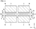
- FIG. 6 is a sectional view of the capacitor module taken along line B-B illustrated in FIG. 4 ;
- FIG. 7 is an enlarged plan view of main elements of a substrate of the capacitor module illustrated in FIG. 3 ;
- FIG. 8 is a sectional view for explaining a crack ratio of a crack occurring in a soldered part
- FIG. 9 is a graph illustrating a result obtained by measuring a crack ratio in a soldered part after a heat cycle test
- FIG. 10 is a plan view illustrating main elements of another configuration example of the capacitor module to which the present invention is applied.
- FIG. 11 is a plan view illustrating another configuration example of the capacitor module to which the present invention is applied.
- FIG. 1 is a configuration diagram illustrating an example of the wireless power transmission system 100 .
- FIG. 2 is a circuit diagram illustrating a configuration of a power transmission side resonator 203 and a power reception side resonator 301 of the wireless power transmission system 100 .
- the wireless power transmission system 100 of the present embodiment is obtained by applying the present invention to a non-contact charging system that performs non-contact charging for a battery (a second battery) installed in an electric vehicle EV as illustrated in FIG. 1 and FIG. 2 .
- the electric vehicle EV is an electrically driven vehicle (a moving body) that travels when a motor is driven using the power charged into the battery.
- the wireless power transmission system 100 of the present embodiment performs wireless power transmission by using a magnetic field resonance method, and includes a wireless power transmission device (hereinafter, referred to a “power transmission device”) 200 installed on the ground G of a charging equipment side and a wireless power reception device (hereinafter, referred to a “power reception device”) 300 installed in the electric vehicle EV.
- a wireless power transmission device hereinafter, referred to a “power transmission device” 200 installed on the ground G of a charging equipment side
- a wireless power reception device hereinafter, referred to a “power reception device” 300 installed in the electric vehicle EV.
- the power transmission device 200 generally includes a power supply circuit 201 , a driving circuit 202 , and the power transmission side resonator 203 .
- the power reception device 300 generally includes the power reception side resonator 301 and a load 302 .
- the load 302 is composed of a rectification circuit 303 and a variable load Vload.
- the power supply circuit 201 serves as an AC/DC power supply that is electrically connected to an external commercial power supply P and converts AC power inputted from the commercial power supply P to desired DC power.
- the power supply circuit 201 is electrically connected to the driving circuit 202 .
- the power supply circuit 201 supplies the converted DC power to the driving circuit 202 .
- the power supply circuit 201 outputs DC power to the driving circuit 202 , and the configuration of the power supply circuit 201 is not particularly limited.
- the power supply circuit 201 there may be a power supply circuit obtained by combining a rectification circuit, which rectifies AC power and converts the rectified AC power to DC power, with a power factor correction (PFC) circuit, which performs power factor improvement, a power supply circuit obtained by combining the same rectification circuit with a switching circuit such as a switching converter, and the like.
- PFC power factor correction
- the driving circuit 202 converts the DC power supplied from the power supply circuit 201 to high frequency power.
- the driving circuit 202 for example, there may be a switching circuit, in which a plurality of switching elements are connected to one another on a bridge basis, and the like.
- the driving circuit 202 is electrically connected to the power transmission side resonator 203 .
- the driving circuit 202 supplies the power transmission side resonator 203 with high frequency power with a driving frequency controlled on the basis of a resonance frequency of the power transmission side resonator 203 .
- the power transmission side resonator 203 constitutes an LC resonance circuit including a power transmission side coil L 1 and a power transmission side capacitor C 1 .
- the resonance frequency of the power transmission side resonator 203 side is caused to become close to the resonance frequency of the power reception side resonator 301 side (or to coincide with the resonance frequency of the power reception side resonator 301 side), so that wireless power transmission using a magnetic field resonance method is possible.
- the power transmission side resonator 203 of the present embodiment has a configuration in which a reactor Ls is serially inserted into the power transmission side capacitor C 1 .
- a reactor Ls is serially inserted into the power transmission side capacitor C 1 .
- the reactor Ls has high impedance with respect to a frequency component sufficiently higher than the resonance frequency of the power transmission side resonator 203 side. In this way, the reactor Ls serves as a filter that supplies the power transmission side coil L 1 with power with no high frequency component.
- the power transmission side coil L 1 for example, is configured by a coil for wireless power transmission in which a Litz wire including copper, aluminum and the like has been spirally wound.
- the power transmission side coil L 1 of the present embodiment is installed on the ground G or is buried in the ground G to face a lower side of a floor of the electric vehicle EV.
- the power transmission side coil L 1 (the power transmission side resonator 203 ) is configured to be installed on the ground G together with the power supply circuit 201 .
- the power transmission side capacitor C 1 has a function of adjusting a driving frequency and both end voltages of the load 302 .
- the power transmission side capacitor C 1 of the present embodiment is configured by a first capacitor C 11 serially connected to the power transmission side coil L 1 and a second capacitor C 12 connected to the power transmission side coil L 1 in a parallel manner; however, the present invention is not limited to such a configuration.
- the power transmission side capacitor C 1 may be configured to include only the first capacitor C 11 serially connected to the power transmission side coil L 1 .
- the power reception side resonator 301 constitutes an LC resonance circuit including a power reception side coil L 2 and a power reception side capacitor C 2 .
- the resonance frequency of the power reception side resonator 301 side is caused to become close to the resonance frequency of the power transmission side resonator 203 side (or to coincide with the resonance frequency of the power transmission side resonator 203 side), so that wireless power transmission using the magnetic field resonance method is possible.
- the power reception side resonator 301 of the present embodiment has a configuration in which a reactor Lr is serially inserted into the power reception side capacitor C 2 .
- the reactor Lr has high impedance with respect to a frequency component sufficiently higher than the resonance frequency of the power reception side resonator 301 side. In this way, the reactor Lr serves as a filter that supplies the load 302 with power with no high frequency component.
- the power reception side coil L 2 for example, is configured by a coil for wireless power transmission in which a Litz wire including copper, aluminum and the like has been spirally wound.
- the power reception side coil L 2 of the present embodiment is installed under the floor of the electric vehicle EV to face the power transmission side coil L 1 installed on the ground G or buried in the ground G.
- the power reception side capacitor C 2 has a function of adjusting a driving frequency and both end voltages of the load 302 .
- the power reception side capacitor C 2 of the present embodiment is configured by a third capacitor C 21 serially connected to the power reception side coil L 2 and a fourth capacitor C 22 connected to the power reception side coil L 2 in a parallel manner; however, the present invention is not limited to such a configuration.
- the power reception side capacitor C 2 may be configured to include only the third capacitor C 21 serially connected to the power reception side coil L 2 .
- the rectification circuit 303 is electrically connected to the power reception side resonator 301 , rectifies the high frequency power received in the power reception side coil L 2 , and converts the rectified high frequency power to DC power.
- the rectification circuit 303 for example, there may be a half-wave rectification circuit composed of one switching element or a diode and a smoothing capacitor, a full wave rectification circuit composed of four switching elements connected to one another on a bridge basis or a diode and a smoothing capacitor, and the like.
- the rectification circuit 303 is electrically connected to the variable load Vload.
- the rectification circuit 303 supplies the converted DC power to the variable load Vload.
- a charger may be provided between the rectification circuit 303 and the variable load Vload.
- the variable load Vload is connected between output terminals of the rectification circuit 303 and stores or consumes the DC power supplied from the rectification circuit 303 .
- the variable load Vload there may be a battery, a motor and the like installed in the electric vehicle EV.
- the variable load Vload can be regarded as a resistive load in which an equivalent resistance value of the load 302 changes according to the passage of time due to a demand state (a storage state or a consumption state) of power. Since an amount of power consumed in the rectification circuit 303 is sufficiently smaller than that in the variable load Vload, the equivalent resistance value of the load 302 may be regarded as being approximate to an equivalent resistance value of the variable load Vload.
- the wireless power transmission system 100 having the above configuration of the present embodiment, it is possible to transmit power in a wireless manner toward the power reception device 300 from the power transmission device 200 by a magnetic field resonance method using a resonance phenomenon between the power transmission side resonator 203 and the power reception side resonator 301 . That is, in the magnetic field resonance method, the resonance frequencies of these two resonators 203 and 301 are caused to become close to each other (or to coincide with each other), and high frequency current and voltage around the resonance frequency are applied to the power transmission side resonator 203 , so that power can be transmitted (supplied) to the electromagnetically resonated power reception side resonator 301 in a wireless manner.
- the wireless power transmission system 100 of the present embodiment it is possible to perform non-contact charging for a battery installed in the electric vehicle EV while transmitting power supplied from the charging equipment side to the electric vehicle EV in a wireless manner without connection to a charging cable.
- capacitor module 1 illustrated in FIG. 3 to FIG. 7 will be described for example.
- FIG. 3 is a plan view illustrating a configuration of the capacitor module 1 .
- FIG. 4 is an enlarged plan view of main elements of the capacitor module 1 .
- FIG. 5 is a sectional view of the capacitor module 1 taken along line A-A illustrated in FIG. 4 .
- FIG. 6 is a sectional view of the capacitor module 1 taken along line B-B illustrated in FIG. 4 .
- FIG. 7 is an enlarged plan view of main elements of a substrate 2 of the capacitor module 1 .
- an X axis direction is a first direction on a horizontal plane of the capacitor module 1
- a Y axis direction is a second direction on the horizontal plane of the capacitor module 1
- a Z axis direction is a thickness direction of the capacitor module 1 .
- the capacitor module 1 of the present embodiment includes the substrate 2 having a first principal surface 2 a and a second principal surface 2 b opposite to each other in the thickness direction, and a capacitor element group 30 including a plurality of capacitor elements 3 disposed in an array on at least the first principal surface 2 a (both principal surfaces 2 a and 2 b in the present embodiment) of the substrate 2 as illustrated in FIG. 3 to FIG. 7 .
- the capacitor module 1 of the present embodiment has a structure in which the plurality of capacitor elements 3 are mounted at overlapping positions on the first principal surface 2 a and the second principal surface 2 b in the plan view. That is, the capacitor module 1 basically has the same mounting structure (a symmetrical structure in which the substrate 2 is interposed between the first principal surface 2 a and the second principal surface 2 b ) at the first principal surface 2 a side and the second principal surface 2 b side of the substrate 2 .
- the mounting structure of the first principal surface (an upper surface) 2 a side of the substrate 2 will be described, and unless otherwise specifically mentioned, the mounting structure of the second principal surface (a lower surface) 2 b side of the substrate 2 will not be described.
- the capacitor element group 30 has a plurality of capacitor element arrays 3 A in which the plurality of capacitor elements 3 disposed in the first direction (the X axis direction) of the first direction and the second direction (the Y axis direction) are serially connected to one another, and has a structure in which the plurality of capacitor element arrays 3 A disposed in the second direction are connected in parallel to one another, wherein the first direction and the second direction cross each other (are orthogonal to each other in the present embodiment) on the plane of the substrate 2 .
- the substrate 2 includes a double-sided printed wiring substrate in which a plurality of wiring patterns are provided on both surfaces of an insulating substrate formed in an approximately rectangular flat plate shape as a whole.
- the substrate 2 has a first wiring 4 a that electrically connects the capacitor elements 3 , which are adjacent to one another in the first direction among the plurality of capacitor elements 3 constituting the capacitor element array 3 A, to one another, a second wiring 4 b that electrically connects the capacitor elements 3 , which are positioned at one end side of the plurality of capacitor element arrays 3 A in the first direction among the plurality of capacitor elements 3 constituting the capacitor element array 3 A, to one another in the second direction, and a third wiring 4 c that electrically connects the capacitor elements 3 , which are positioned at the other end side of the plurality of capacitor element arrays 3 A in the first direction among the plurality of capacitor elements 3 constituting the capacitor element array 3 A, to one another in the second direction.
- a first pad electrode 5 a and a second pad electrode 5 b are provided at positions of the substrate 2 corresponding to each capacitor element 3 .
- the first pad electrode 5 a and the second pad electrode 5 b are obtained by patterning a part of the wirings 4 a to 4 c called lands in a rectangular shape.
- the first pad electrode 5 a and the second pad electrode 5 b have the same shape and are juxtaposed in the first direction.
- the plurality of capacitor elements 3 include laminated ceramic chip capacitors formed in an approximately rectangular shape in the plan view.
- Each of the capacitor elements 3 has a first terminal electrode 6 a provided along an end edge in a short direction (the second direction) at one end side in a longitudinal direction (the first direction) thereof, and a second terminal electrode 6 b provided along an end edge in the short direction (the second direction) at the other end side in the longitudinal direction (the first direction) thereof.
- Each of the capacitor elements 3 is mounted on the substrate 2 via a first soldered part 7 a in which the first terminal electrode 6 a and the first pad electrode 5 a are solder-bonded to each other, and a second soldered part 7 b in which the second terminal electrode 6 b and the second pad electrode 5 b are solder-bonded to each other. In this way, each of the capacitor elements 3 is mounted on the substrate 2 bridging between the first pad electrode 5 a and the second pad electrode 5 b.
- the capacitor module 1 of the present embodiment has a plurality of penetrating holes 8 formed at positions corresponding to the plurality of capacitor elements 3 to pass through the substrate 2 in the thickness direction (the Z axis direction).
- the penetrating holes 8 have a circular shape in the plan view and are provided at positions, which overlap a pair of boundary lines S 1 and S 2 that define a boundary between at least a region E between the first pad electrode 5 a and the second pad electrode 5 b and an outside of the region E, in the plan view.
- each of the penetrating holes 8 is provided at a position overlapping an outline of each of the capacitor elements 3 mounted on the substrate 2 in the plan view.
- the pair of boundary lines S 1 and S 2 are linear lines that connect the end edges of the first pad electrode 5 a and the second pad electrode 5 b along the first direction (the X axis direction) to each other. Furthermore, the pair of boundary lines S 1 and S 2 constitute lines approximately coinciding with the outlines of the capacitor elements 3 mounted on the substrate 2 along the first direction (the X axis direction).
- the region E is a region surrounded by the end edges of the first pad electrode 5 a and the second pad electrode 5 b along the second direction (the Y axis direction), in which they face each other, and the pair of boundary lines S 1 and S 2 .
- the penetrating hole 8 includes regions 8 a inward from the boundary lines S 1 and S 2 and regions 8 b outward from the boundary lines S 1 and S 2 in the plan view. Furthermore, the penetrating hole 8 includes a region overlapping the capacitor element 3 and a region not overlapping the capacitor element 3 in the plan view.
- such penetrating holes 8 are provided, so that it is possible to suppress the occurrence of solder cracking in the first and second soldered parts 7 a and 7 b.
- the penetrating holes 8 are provided at positions overlapping the pair of boundary lines S 1 and S 2 in the plan view, so that it is possible to reduce creep strain occurring in the first and second soldered parts 7 a and 7 b . That is, a point indicating a maximum value of the creep strain, exists on the pair of boundary lines S 1 and S 2 . And a crack progresses with this point as a starting point. Consequently, the penetrating holes 8 are provided on the pair of boundary lines S 1 and S 2 , so that it is possible to suppress the occurrence of cracking.
- the capacitor module 1 of the present embodiment it is possible to improve a lifespan according to disconnection in the first and second soldered parts 7 a and 7 b while suppressing the occurrence of solder cracking in the first and second soldered parts 7 a and 7 b.
- the penetrating holes 8 are provided in the state of overlapping the boundary line S 1 of one capacitor element 3 side and the boundary line S 2 of the other capacitor element 3 side in the plan view, wherein the one capacitor element 3 and the other capacitor element 3 are adjacent to each other among the plurality of capacitor elements 3 disposed in the second direction (the Y axis direction).
- the penetrating hole 8 can be used in common between one capacitor element 3 and the another capacitor element 3 adjacent to each other, as compared with a case where two penetrating holes 8 overlapping the pair of boundary lines S 1 and S 2 are provided for each capacitor element 3 . Consequently, it is possible to suppress the occurrence of solder cracking in the first and second soldered parts 7 a and 7 b using less penetrating holes 8 .
- the penetrating holes 8 are provided in the state of overlapping the pair of boundary lines S 1 and S 2 , which define the region E between the first pad electrode 5 a and the second pad electrode 5 b of the first principal surface 2 a side, and the pair of boundary lines S 1 and S 2 , which define the region E between the first pad electrode 5 a and the second pad electrode 5 b of the second principal surface 2 b side, in the plan view.
- the penetrating holes 8 can be used in common between the first principal surface 2 a side and the second principal surface 2 b side of the substrate 2 . In this way, it is possible to achieve miniaturization and integration of the capacitor module 1 while suppressing the occurrence of solder cracking in the first and second soldered parts 7 a and 7 b.
- the capacitor module 1 of the present embodiment when a length (hereinafter, referred to as an “inter-electrode length”) on the boundary lines S 1 and S 2 between the first pad electrode 5 a and the second pad electrode 5 b is set as L and a length (hereinafter, referred to as a “hole length”) on the boundary lines S 1 and S 2 of the penetrating hole 8 is set as D, it is preferable to satisfy a relation of the following (1). 0.15 ⁇ D/L ⁇ 0.85 (1)
- a capacitor element 3 having a 3225 size (an external size is 3.2 mm ⁇ 2.5 mm) was mounted on the substrate 2 provided with the first and second pad electrodes 5 a and 5 b having an external size of 2.2 mm ⁇ 2.5 mm and an inter-electrode length L of 1.3 mm. Furthermore, the substrate 2 was provided with the penetrating hole 8 in which the hole length D was changed for each capacitor element array 3 A.
- a crack ratio of a crack occurred in the first and second soldered parts 7 a and 7 b was calculated for each hole length D.
- the crack ratio is a value calculated using the following (2) when the length of a crack occurring in the first and second soldered parts 7 a and 7 b is set as L 1 and the shortest length existing in the first and second soldered parts 7 a and 7 b is set as L 2 as illustrated in FIG. 8 .
- Crack ratio (%) ⁇ L 1/( L 1+ L 2) ⁇ 100 (2)
- an average value of the crack ratios was calculated for the capacitor element arrays 3 A in which the hole lengths D were different from one another. Then, for the presence or absence of the occurrence of the solder cracking, an optimal hole length D was calculated employing a position, in which the crack ratio was 50%, as a reference. The results are collectively illustrated in the graph of FIG. 9 .
- the capacitor module 1 of the present embodiment when the relation of the above (1) is satisfied, it is possible to reduce the occurrence of the solder cracking in the first and second soldered parts 7 a and 7 b and to extend fatigue life of the capacitor module 1 according to the heat cycle while keeping the mechanical strength of the substrate 2 .
- the penetrating hole 8 having a circular shape in the plan view is formed due to ease of machining of the substrate 2 ; however, the present invention is not limited to the shape of the penetrating hole 8 and for example, it is also possible to form the penetrating hole 8 having an oval shape, a long hole shape, other shapes and the like in the plan view.
- the outline of the capacitor element 3 and the pair of boundary lines S 1 and S 2 approximately coincide with each other due to a self-alignment effect due to mounting.
- a case, where the outline of the capacitor element 3 and the pair of boundary lines S 1 and S 2 do not coincide with each other due to a difference between sizes and the like of the first and second terminal electrodes 6 a and 6 b (chips) and the first and second pad electrodes 5 a and 5 b (lands) may also be conceived.
- the hole length D of the penetrating hole 8 on the pair of boundary lines S 1 and S 2 is decided by deciding the position of the penetrating hole 8 based on the boundary lines S 1 and S 2 and considering a deviation amount of the outline of the capacitor element 3 with respect to the pair of boundary lines S 1 and S 2 .
- the capacitor module 1 of the present embodiment has a first connection terminal 10 a electrically connected to one end side of the second wiring 4 b in the second direction, and a second connection terminal 10 b electrically connected to the other end side of the third wiring 4 c in the second direction as illustrated in FIG. 3 .
- the first connection terminal 10 a and the second connection terminal 10 b are external connection terminals of the capacitor module 1 , and are provided on land parts 11 a and 11 b protruding in a rectangular shape outward in the first direction from one end side of the second wiring 4 b and the other end side of the third wiring 4 c .
- the first connection terminal 10 a and the second connection terminal 10 b are provided at symmetrical positions (diagonal positions in the present embodiment) while the capacitor element group 30 is interposed between in the plane of the substrate 2 .
- a current path from one connection terminal (the first connection terminal 10 a in the present embodiment) to the other connection terminal (the second connection terminal 10 b in the present embodiment) can be equalized among the capacitor element arrays 3 A constituting the capacitor element group 30 .
- a current inputted from the first connection terminal 10 a reaches the other end side from one end side of each capacitor element array 3 A constituting the capacitor element group 30 via the second wiring 4 b , and is outputted to the second connection terminal 10 b via the third wiring 4 c.
- the length of the current path of a current I 1 flowing through the capacitor element array 3 A positioned at one end side in the second direction, the length of the current path of a current I 2 flowing through the capacitor element array 3 A positioned at the center side in the second direction, and the length of the current path of a current I 3 flowing through the capacitor element array 3 A positioned at the other end side in the second direction are identical to one another between the first connection terminal 10 a and the second connection terminal 10 b.
- the currents I 1 to I 3 can approximately equally flow through the plurality of capacitor elements 3 mounted on the substrate 2 . Consequently, in the capacitor module 1 of the present embodiment, it is possible to suppress generation of heat from each capacitor element 3 while avoiding the probability that the current will be concentrated on some capacitor elements 3 and these capacitor elements 3 will break.
- the capacitor module 1 of the present embodiment has a structure in which the plurality of capacitor elements 3 are mounted at overlapping positions on the first principal surface 2 a and the second principal surface 2 b in the plan view. In such a case, it is possible to achieve miniaturization and integration of the capacitor module 1 while suppressing the generation of heat from each capacitor element 3 on both principal surfaces 2 a and 2 b of the substrate 2 .
- the first connection terminal 10 a and the second connection terminal 10 b are provided at diagonal positions while interposing the capacitor element group 30 therebetween in the plane of the substrate 2 .
- the capacitor module 1 of the present embodiment can be preferably used as the power transmission side capacitor C 1 and the power reception side capacitor C 2 respectively constituting the power transmission side resonator 203 and the power reception side resonator 301 . That is, the capacitor module 1 of the present embodiment can constitute the power transmission side capacitor C 1 and the power reception side capacitor C 2 compatible with the power transmission side resonator 203 and the power reception side resonator 301 to which large capacity of high frequency current and voltage are applied.
- the wireless power transmission system 100 of the present embodiment it is possible to stably perform wireless power transmission by using the magnetic field resonance method between the power transmission device 200 including such a power transmission side resonator 203 and the power reception device 300 including such a power reception side resonator 301 .
- a penetrating hole 9 may be provided between the pair of boundary lines S 1 and S 2 to pass through the substrate 2 in the thickness direction.
- the penetrating hole 9 having a circular shape in the plan view is provided between (at the center in the present embodiment) the penetrating holes 8 provided at positions overlapping the pair of boundary lines S 1 and S 2 in the plan view.
- the penetrating hole 9 may have an oval shape, a long hole shape, other shapes and the like in the plan view, similarly to the penetrating hole 8 .
- the opening area (the hole diameter) of the penetrating hole 8 provided at the position overlapping the pair of boundary lines S 1 and S 2 in the plan view is larger than the opening area (the hole diameter) of the penetrating hole 9 positioned between the pair of boundary lines S 1 and S 2 .
- the opening area (the hole diameter) of the penetrating hole 9 it is possible to further reduce creep strain occurring in the first and second soldered parts 7 a and 7 b while preventing the opening area (the hole diameter) of the penetrating hole 9 from being excessively increased, so that it is possible to further suppress the occurrence of solder cracking in the first and second soldered parts 7 a and 7 b.
- the aforementioned capacitor module 1 is not limited to the configuration in which the first connection terminal 10 a and the second connection terminal 10 b are provided at diagonal positions while interposing the capacitor element group 30 therebetween.
- first connection terminal 10 a can be moved around the center of the capacitor element group 30 in the second direction from the diagonal position of the capacitor element group 30 due to the first extension wiring 4 d.
- the lengths of current paths from the first connection terminal 10 a to the second connection terminal 10 b can be equalized among the capacitor element arrays 3 A constituting the capacitor element group 30 regardless of the extension length of the first extension wiring 4 d or the second extension wiring 4 e . Consequently, it is possible to improve the degree of freedom in design of the arrangement of the first connection terminal 10 a and the second connection terminal 10 b while suppressing the generation of heat from each capacitor element 3 .
- the present embodiment has described a case where the present invention is applied to a non-contact charging system that performs non-contact charging for a battery installed in the electric vehicle EV; however, the present invention can also be widely applied to an electrically driven vehicle (a moving body) such as a plug-in hybrid vehicle (PHEV), in addition to the electric vehicle EV.
- a moving body such as a plug-in hybrid vehicle (PHEV)
- PHEV plug-in hybrid vehicle
- a power transmission system employing the present invention is not limited to such a non-contact charging system.
- the present invention can also be widely applied to a non-contact charging system that performs non-contact charging for a portable electronic device such as a tablet terminal and a personal computer (PC) placed on a table, a non-contact power feeding system that performs non-contact power feeding for an electrically driven vehicle which is traveling, and the like.
- a non-contact charging system that performs non-contact charging for a portable electronic device such as a tablet terminal and a personal computer (PC) placed on a table
- PC personal computer
Landscapes
- Engineering & Computer Science (AREA)
- Power Engineering (AREA)
- Microelectronics & Electronic Packaging (AREA)
- Manufacturing & Machinery (AREA)
- Computer Networks & Wireless Communication (AREA)
- Transportation (AREA)
- Mechanical Engineering (AREA)
- Fixed Capacitors And Capacitor Manufacturing Machines (AREA)
- Electric Propulsion And Braking For Vehicles (AREA)
- Charge And Discharge Circuits For Batteries Or The Like (AREA)
Abstract
Description
- [Patent Document 1] Japanese Unexamined Patent Application, First Publication No. 2017-005790
- [Patent Document 2] Japanese Unexamined Patent Application, First Publication No. 2017-051084
- [Patent Document 3] Japanese Unexamined Patent Application, First Publication No. 2016-018802
- [Patent Document 4] Japanese Unexamined Patent Application, First Publication No. 2001-326444
- [Patent Document 5] PCT International Publication No. WO 2009/096003 [Patent Document 6] Japanese Unexamined Patent Application, First Publication No. 2003-324030
0.15≤D/L≤0.85 (1)
Crack ratio (%)={L1/(L1+L2)}×100 (2)
-
- 1 Capacitor module
- 2 Substrate
- 2 a First principal surface
- 2 b Second principal surface
- 3 Capacitor element
- 4 a First wiring
- 4 b Second wiring
- 4 c Third wiring
- 5 a First pad electrode
- 5 b Second pad electrode
- 6 a First terminal electrode
- 6 b Second terminal electrode
- 7 a First soldered part
- 7 b Second soldered part
- 8, 9 Through hole
- E Region
- S1, S2 Boundary line
- 100 Wireless power transmission system
- 200 Wireless power transmission device
- 201 Power supply circuit
- 202 Driving circuit
- 203 Power transmission side resonator
- 300 Wireless power reception device
- 301 Power reception side resonator
- 302 Load
- 303 Rectification circuit
- L1 Power transmission side coil
- L2 Power reception side coil
- C1 Power transmission side capacitor
- C2 Power reception side capacitor
- EV Electric vehicle
Claims (18)
Applications Claiming Priority (2)
| Application Number | Priority Date | Filing Date | Title |
|---|---|---|---|
| JP2017213477A JP2019087592A (en) | 2017-11-06 | 2017-11-06 | Capacitor module, resonator, wireless power transmission device, wireless power reception device, and wireless power transmission system |
| JP2017-213477 | 2017-11-06 |
Publications (2)
| Publication Number | Publication Date |
|---|---|
| US20190141835A1 US20190141835A1 (en) | 2019-05-09 |
| US10881002B2 true US10881002B2 (en) | 2020-12-29 |
Family
ID=66327983
Family Applications (1)
| Application Number | Title | Priority Date | Filing Date |
|---|---|---|---|
| US16/179,038 Active 2039-02-26 US10881002B2 (en) | 2017-11-06 | 2018-11-02 | Capacitor module, resonator, wireless power transmission device, wireless power reception device, and wireless power transmission system |
Country Status (3)
| Country | Link |
|---|---|
| US (1) | US10881002B2 (en) |
| JP (1) | JP2019087592A (en) |
| CN (1) | CN109767912B (en) |
Families Citing this family (2)
| Publication number | Priority date | Publication date | Assignee | Title |
|---|---|---|---|---|
| DE102018205141A1 (en) * | 2018-04-05 | 2019-10-10 | Siemens Aktiengesellschaft | Vibration-damped circuit arrangement, converter and aircraft with such an arrangement |
| JP7218677B2 (en) * | 2019-06-17 | 2023-02-07 | 株式会社オートネットワーク技術研究所 | Substrate structure |
Citations (17)
| Publication number | Priority date | Publication date | Assignee | Title |
|---|---|---|---|---|
| JP2001326444A (en) | 2000-05-12 | 2001-11-22 | Clarion Co Ltd | Chip component mounting board |
| JP2003324030A (en) | 2002-04-26 | 2003-11-14 | Taiyo Yuden Co Ltd | Method of mounting capacitor on circuit board and circuit board for mounting capacitor |
| US20050225408A1 (en) * | 2004-04-08 | 2005-10-13 | Fujitsu Limited | Direct current cut structure |
| US7036217B2 (en) * | 2001-06-22 | 2006-05-02 | Intel Corporation | Methods of manufacturing via intersect pad for electronic components |
| US20080218984A1 (en) * | 2005-08-18 | 2008-09-11 | Tdk Corporation | Flexible substrate, mounted structure, display unit, and portable electronic apparatus |
| WO2009096003A1 (en) | 2008-01-29 | 2009-08-06 | Fujitsu Limited | Mounting structure for chip capacitor, electronic device and mounting method |
| US20110222255A1 (en) * | 2010-03-10 | 2011-09-15 | Panasonic Corporation | Electronic circuit |
| US8212152B2 (en) * | 2008-04-28 | 2012-07-03 | Tdk Corporation | Electronic device |
| US20140111021A1 (en) * | 2011-06-30 | 2014-04-24 | Toyota Jidosha Kabushiki Kaisha | Power transmission device, power reception device and power transfer system |
| US9089054B2 (en) * | 2012-06-12 | 2015-07-21 | Murata Manufacturing Co., Ltd. | Chip-component structure |
| US20150270065A1 (en) * | 2014-03-24 | 2015-09-24 | Murata Manufacturing Co., Ltd. | Electronic component |
| JP2016018802A (en) | 2014-07-04 | 2016-02-01 | トヨタ自動車株式会社 | Coil unit |
| US20160308403A1 (en) * | 2015-04-14 | 2016-10-20 | Minnetronix, Inc. | Repeater resonator |
| JP2017005790A (en) | 2015-06-05 | 2017-01-05 | Tdk株式会社 | Wireless power transmission system |
| US20170063163A1 (en) | 2015-09-02 | 2017-03-02 | Tdk Corporation | Coil device and wireless power transmission device |
| US20170063157A1 (en) * | 2015-09-02 | 2017-03-02 | Semiconductor Components Industries, Llc | Tunable/de-tunable wireless power resonator system and related methods |
| JP2017051084A (en) | 2015-09-02 | 2017-03-09 | Tdk株式会社 | Coil device and wireless power transmission device |
Family Cites Families (5)
| Publication number | Priority date | Publication date | Assignee | Title |
|---|---|---|---|---|
| JPH098444A (en) * | 1995-04-20 | 1997-01-10 | Sony Corp | Electronic circuit device |
| JP2013239470A (en) * | 2012-05-11 | 2013-11-28 | Fuji Electric Fa Components & Systems Co Ltd | Surface mounting substrate |
| JP2014099589A (en) * | 2012-10-19 | 2014-05-29 | Murata Mfg Co Ltd | Method of manufacturing mounting substrate on which multilayer ceramic capacitors are mounted and mounting structure body |
| KR101514536B1 (en) * | 2013-08-09 | 2015-04-22 | 삼성전기주식회사 | Chip electronic component and board for mounting the same |
| JP6370558B2 (en) * | 2014-02-14 | 2018-08-08 | 矢崎総業株式会社 | Coil unit and power supply system having the same |
-
2017
- 2017-11-06 JP JP2017213477A patent/JP2019087592A/en active Pending
-
2018
- 2018-11-02 CN CN201811300009.9A patent/CN109767912B/en active Active
- 2018-11-02 US US16/179,038 patent/US10881002B2/en active Active
Patent Citations (17)
| Publication number | Priority date | Publication date | Assignee | Title |
|---|---|---|---|---|
| JP2001326444A (en) | 2000-05-12 | 2001-11-22 | Clarion Co Ltd | Chip component mounting board |
| US7036217B2 (en) * | 2001-06-22 | 2006-05-02 | Intel Corporation | Methods of manufacturing via intersect pad for electronic components |
| JP2003324030A (en) | 2002-04-26 | 2003-11-14 | Taiyo Yuden Co Ltd | Method of mounting capacitor on circuit board and circuit board for mounting capacitor |
| US20050225408A1 (en) * | 2004-04-08 | 2005-10-13 | Fujitsu Limited | Direct current cut structure |
| US20080218984A1 (en) * | 2005-08-18 | 2008-09-11 | Tdk Corporation | Flexible substrate, mounted structure, display unit, and portable electronic apparatus |
| WO2009096003A1 (en) | 2008-01-29 | 2009-08-06 | Fujitsu Limited | Mounting structure for chip capacitor, electronic device and mounting method |
| US8212152B2 (en) * | 2008-04-28 | 2012-07-03 | Tdk Corporation | Electronic device |
| US20110222255A1 (en) * | 2010-03-10 | 2011-09-15 | Panasonic Corporation | Electronic circuit |
| US20140111021A1 (en) * | 2011-06-30 | 2014-04-24 | Toyota Jidosha Kabushiki Kaisha | Power transmission device, power reception device and power transfer system |
| US9089054B2 (en) * | 2012-06-12 | 2015-07-21 | Murata Manufacturing Co., Ltd. | Chip-component structure |
| US20150270065A1 (en) * | 2014-03-24 | 2015-09-24 | Murata Manufacturing Co., Ltd. | Electronic component |
| JP2016018802A (en) | 2014-07-04 | 2016-02-01 | トヨタ自動車株式会社 | Coil unit |
| US20160308403A1 (en) * | 2015-04-14 | 2016-10-20 | Minnetronix, Inc. | Repeater resonator |
| JP2017005790A (en) | 2015-06-05 | 2017-01-05 | Tdk株式会社 | Wireless power transmission system |
| US20170063163A1 (en) | 2015-09-02 | 2017-03-02 | Tdk Corporation | Coil device and wireless power transmission device |
| US20170063157A1 (en) * | 2015-09-02 | 2017-03-02 | Semiconductor Components Industries, Llc | Tunable/de-tunable wireless power resonator system and related methods |
| JP2017051084A (en) | 2015-09-02 | 2017-03-09 | Tdk株式会社 | Coil device and wireless power transmission device |
Also Published As
| Publication number | Publication date |
|---|---|
| JP2019087592A (en) | 2019-06-06 |
| CN109767912A (en) | 2019-05-17 |
| US20190141835A1 (en) | 2019-05-09 |
| CN109767912B (en) | 2021-07-23 |
Similar Documents
| Publication | Publication Date | Title |
|---|---|---|
| US10158256B2 (en) | Contactless connector system tolerant of position displacement between transmitter coil and receiver coil and having high transmission efficiency | |
| US11837877B2 (en) | Coil module, wireless charging transmitting apparatus, receiving apparatus, system, and terminal | |
| EP3282539B1 (en) | Power transmission device, vehicle equipped with power transmission device, and wireless power transmission system | |
| US9705363B2 (en) | Communication control device and mounting board | |
| EP3016231B1 (en) | Power transmission device, vehicle equipped with power transmission device, and wireless power transmission system | |
| US9224533B2 (en) | Wireless electric power transmission apparatus | |
| JP2016039773A (en) | Power transmission device and wireless power transmission system | |
| US20110248573A1 (en) | Wireless power transmission system | |
| JP2016039644A (en) | Power transmission device and wireless power transmission system | |
| CN106952710A (en) | A wireless charging magnetic coupling structure and its circuit for multiple loads | |
| US10291080B2 (en) | Electric power transmission device and wireless electric power transfer system | |
| US10881002B2 (en) | Capacitor module, resonator, wireless power transmission device, wireless power reception device, and wireless power transmission system | |
| US9473212B2 (en) | Wireless power transmission system | |
| JP2016093088A (en) | Power transmission device, vehicle having the same and radio power transmission system | |
| JP2012143092A (en) | Charging ac adapter | |
| US10056788B2 (en) | Wireless transmission device | |
| US20190140478A1 (en) | Capacitor module, resonator, wireless power transmission device, wireless power reception device, and wireless power transmission system | |
| CN110323837B (en) | Coil unit, wireless power feeding device, wireless power receiving device, and wireless power transmission system | |
| EP3790162B1 (en) | Wireless charging apparatus for preventing magnetic field cancellation between adjacent coils | |
| US20120200282A1 (en) | Chip electronic component, mounted structure of chip electronic component, and switching supply circuit | |
| JP6088814B2 (en) | Wireless power transmission system |
Legal Events
| Date | Code | Title | Description |
|---|---|---|---|
| AS | Assignment |
Owner name: TDK CORPORATION, JAPAN Free format text: ASSIGNMENT OF ASSIGNORS INTEREST;ASSIGNOR:FURUKAWA, KENJI;REEL/FRAME:047394/0465 Effective date: 20181005 |
|
| FEPP | Fee payment procedure |
Free format text: ENTITY STATUS SET TO UNDISCOUNTED (ORIGINAL EVENT CODE: BIG.); ENTITY STATUS OF PATENT OWNER: LARGE ENTITY |
|
| STPP | Information on status: patent application and granting procedure in general |
Free format text: DOCKETED NEW CASE - READY FOR EXAMINATION |
|
| STPP | Information on status: patent application and granting procedure in general |
Free format text: PUBLICATIONS -- ISSUE FEE PAYMENT VERIFIED |
|
| STCF | Information on status: patent grant |
Free format text: PATENTED CASE |
|
| MAFP | Maintenance fee payment |
Free format text: PAYMENT OF MAINTENANCE FEE, 4TH YEAR, LARGE ENTITY (ORIGINAL EVENT CODE: M1551); ENTITY STATUS OF PATENT OWNER: LARGE ENTITY Year of fee payment: 4 |