US10879654B2 - RF PCB connector with a surface-mount interface - Google Patents
RF PCB connector with a surface-mount interface Download PDFInfo
- Publication number
- US10879654B2 US10879654B2 US16/712,426 US201916712426A US10879654B2 US 10879654 B2 US10879654 B2 US 10879654B2 US 201916712426 A US201916712426 A US 201916712426A US 10879654 B2 US10879654 B2 US 10879654B2
- Authority
- US
- United States
- Prior art keywords
- pcb
- surface mount
- housing
- connector
- sections
- Prior art date
- Legal status (The legal status is an assumption and is not a legal conclusion. Google has not performed a legal analysis and makes no representation as to the accuracy of the status listed.)
- Active
Links
- 239000004020 conductor Substances 0.000 claims abstract description 65
- 229910052751 metal Inorganic materials 0.000 claims description 10
- 239000002184 metal Substances 0.000 claims description 10
- 238000005476 soldering Methods 0.000 description 5
- 239000000463 material Substances 0.000 description 3
- 238000012986 modification Methods 0.000 description 2
- 230000004048 modification Effects 0.000 description 2
- 125000006850 spacer group Chemical group 0.000 description 2
- 239000000758 substrate Substances 0.000 description 2
- ATJFFYVFTNAWJD-UHFFFAOYSA-N Tin Chemical compound [Sn] ATJFFYVFTNAWJD-UHFFFAOYSA-N 0.000 description 1
- 238000005452 bending Methods 0.000 description 1
- 230000009286 beneficial effect Effects 0.000 description 1
- -1 led Chemical compound 0.000 description 1
- 150000002739 metals Chemical class 0.000 description 1
- 238000000034 method Methods 0.000 description 1
- 229910052709 silver Inorganic materials 0.000 description 1
- 239000004332 silver Substances 0.000 description 1
Images


Classifications
-
- H—ELECTRICITY
- H01—ELECTRIC ELEMENTS
- H01R—ELECTRICALLY-CONDUCTIVE CONNECTIONS; STRUCTURAL ASSOCIATIONS OF A PLURALITY OF MUTUALLY-INSULATED ELECTRICAL CONNECTING ELEMENTS; COUPLING DEVICES; CURRENT COLLECTORS
- H01R24/00—Two-part coupling devices, or either of their cooperating parts, characterised by their overall structure
- H01R24/38—Two-part coupling devices, or either of their cooperating parts, characterised by their overall structure having concentrically or coaxially arranged contacts
- H01R24/40—Two-part coupling devices, or either of their cooperating parts, characterised by their overall structure having concentrically or coaxially arranged contacts specially adapted for high frequency
- H01R24/42—Two-part coupling devices, or either of their cooperating parts, characterised by their overall structure having concentrically or coaxially arranged contacts specially adapted for high frequency comprising impedance matching means or electrical components, e.g. filters or switches
- H01R24/44—Two-part coupling devices, or either of their cooperating parts, characterised by their overall structure having concentrically or coaxially arranged contacts specially adapted for high frequency comprising impedance matching means or electrical components, e.g. filters or switches comprising impedance matching means
-
- H—ELECTRICITY
- H01—ELECTRIC ELEMENTS
- H01R—ELECTRICALLY-CONDUCTIVE CONNECTIONS; STRUCTURAL ASSOCIATIONS OF A PLURALITY OF MUTUALLY-INSULATED ELECTRICAL CONNECTING ELEMENTS; COUPLING DEVICES; CURRENT COLLECTORS
- H01R24/00—Two-part coupling devices, or either of their cooperating parts, characterised by their overall structure
- H01R24/38—Two-part coupling devices, or either of their cooperating parts, characterised by their overall structure having concentrically or coaxially arranged contacts
- H01R24/40—Two-part coupling devices, or either of their cooperating parts, characterised by their overall structure having concentrically or coaxially arranged contacts specially adapted for high frequency
- H01R24/50—Two-part coupling devices, or either of their cooperating parts, characterised by their overall structure having concentrically or coaxially arranged contacts specially adapted for high frequency mounted on a PCB [Printed Circuit Board]
-
- H—ELECTRICITY
- H05—ELECTRIC TECHNIQUES NOT OTHERWISE PROVIDED FOR
- H05K—PRINTED CIRCUITS; CASINGS OR CONSTRUCTIONAL DETAILS OF ELECTRIC APPARATUS; MANUFACTURE OF ASSEMBLAGES OF ELECTRICAL COMPONENTS
- H05K1/00—Printed circuits
- H05K1/02—Details
- H05K1/0213—Electrical arrangements not otherwise provided for
- H05K1/0237—High frequency adaptations
- H05K1/0243—Printed circuits associated with mounted high frequency components
-
- H—ELECTRICITY
- H01—ELECTRIC ELEMENTS
- H01R—ELECTRICALLY-CONDUCTIVE CONNECTIONS; STRUCTURAL ASSOCIATIONS OF A PLURALITY OF MUTUALLY-INSULATED ELECTRICAL CONNECTING ELEMENTS; COUPLING DEVICES; CURRENT COLLECTORS
- H01R2103/00—Two poles
Definitions
- the invention relates to an RF-PCB connector assembly which may be used for milli-meter waves and which has a surface-mount interface for a printed circuit board (PCB).
- PCB printed circuit board
- An RF connector assembly is disclosed in U.S. Pat. No. 6,607,400 B1.
- a connector is mounted into a cutout of a printed circuit board. The electrical contact is established by soldering pads to a ground plane and to a signal line. Due to its design, as a skilled artisan will readily appreciate, such connector is only suitable for operation at frequencies up to order of magnitude of 1 GHz.
- the connector is a miniature pushbutton connector. A larger connector with a higher weight cannot be mounted by the disclosed PCB interface.
- a millimeter-wave connector for interconnecting a microstrip circuit and an external circuit is disclosed in U.S. Pat. No. 4,669,805.
- the connector is held in a housing, which also contains a microstrip substrate to be connected to the connector.
- the flexible center conductor of the connector has to be bent to adapt to the microstrip circuit. Bending of the center conductor may cause asymmetries, which degrade the electrical characteristics of the connector.
- the embodiments are providing a millimeter-wave connector, which is configured for and can be mounted to a printed circuit board (PCB) or any other microstrip substrate without requiring complex and expensive mounting tools.
- PCB printed circuit board
- the connector should be designed such, that it can be mounted by automated tools.
- a millimeter wave or RF connector for printed circuit boards includes housing, an RF connector interface, and a printed circuit board interface.
- the RF-PCB connector defines a mounting plane.
- the mounting plane is a common plane of all surface mount components of the connector. It is also a plane of a PCB to which the connector may be mounted.
- the RF connector interface may be any standard RF connector interface like SMA, 2.92 mm, 1.85 mm or 1.0 mm.
- the RF connector interface may provide a coaxial connector interface that generally has an outer conductor and an internal conductor (including a center conductor member and/or an inner conductor member).
- the coaxial RF connector interface may be mounted or attached to the housing.
- the outer conductor may be part of the housing, such that it is monolithic with the housing.
- the housing may include a metal block having a cuboid shape.
- the housing includes at least one, or it may include two surface mount sections which may be part of the housing and may be monolithic with the housing.
- the surface mount sections may be formed as side wings to the housing, therefore requiring less space and material. Furthermore, side wings provide lower thermal capacity.
- the at least one surface mount section has a plurality of surface mount studs which may be monolithic with the surface mount section and which have a planar end surface in the mounting plane.
- the surface mount studs may be soldered with their end surface to the surface of a printed circuit board. They may be soldered to a continuous metal surface, like a ground plane.
- the surface mount studs may be soldered to matching contact pads.
- contact pads may be insulated from each other and/or from the system ground, as the ground connection may be done by the matching blocks, which are part of the PCB contact section and are arranged close to the inner conductor exit of the housing.
- the contact pads may also be used for further grounding the connector.
- centering of each surface mount stud to the corresponding contact pad may automatically be done by surface tension of the soldering metal.
- soldering metal may be any metal or combination of metals as known from prior art, e.g. tin, led, silver and others.
- the centering of the individual surface mount studs results in a total alignment of RF connector. Furthermore, the RF connector can easily be handled by automatic pick and place systems and needs no additional handling steps.
- the housing may include a conductive material, which may be a metal.
- the outer conductor can be contacted by means of the surface mount studs to a printed circuit board.
- the center conductor (via its extension, referred to herein as an inner conductor, as will be discussed below) of the coaxial RF connector interface is guided through the housing, which may be within a coaxial bore to maintain the coaxial structure by minimizing reflections.
- the center conductor (member) and the inner conductor (member) form an internal conductor (member) of the coaxial RF connector.
- the inner conductor is disposed to emerge from or exit the housing at the PCB contact section, which may be at a side opposing to the side of the coaxial RF connector interface, and has a contact area in the mounting plane.
- At the exit side of the housing close to the inner conductor is at least one matching block in electrical contact with the housing, which keeps the capacitance of the inner conductor in the area of the exit side and the contact to the strip line of the printed circuit board corresponding to the inductance, such that the characteristic impedance is always constant and the reflections are minimized.
- the matching blocks may also act as soldering pads to provide an electrical connection to a ground plane of the printed circuit board.
- a cutout may be provided in the printed circuit board.
- the cutout may be at least slightly larger than the housing, such that there is a gap between the cutout and the housing. It is not necessary that the cutout exactly matches the housing and holds the housing, as the housing itself is precisely centered by the surface mount studs which are further centered to the contact pads. Such a precision alignment is necessary to provide a perfect alignment at the exit side of the inner conductor with the strip line, which further results in minimal reflections at high frequencies.
- an RF connector system is provided to include at least one RF connector structured as discussed above and a matching printed circuit board, structured as discussed above.
- the contact pads of the printed circuit board may match to the surface mount studs of the RF connector.
- the contact pads and the surface mount studs may have a rectangular, or a squared cross-section.
- the size of the contact pads may be by 0.05 mm to 0.15 mm larger than the size of the surface mount studs.
- the surface mount studs may also have a circular or elliptical shape, whereas the size of the contact pads, which may have a rectangular or circular or elliptical shape, may be in a range from 0.05 to 0.15 mm larger than the studs.
- the housing and/or the surface mount stud as well as the matching blocks may have a surface, which can be soldered easily.
- the surfaces may be electro-plated.
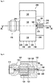
- FIG. 1 shows a perspective view of the RF connector with PCB interface.
- FIG. 2 illustrates a detailed view of a surface mount section.
- FIG. 3 depicts a detail of the inner conductor connection.
- FIG. 4 presents details of a surface mount stud.
- FIG. 5 shows a top view of a RF connector with PCB interface.
- FIG. 6 illustrates a sectional view of the RF connector with PCB interface.
- FIG. 7 provides a side view of the RF connector.
- FIG. 8 shows a bottom view of the RF connector.
- FIG. 9 is an enlarged sectional view of FIG. 7 .
- FIG. 1 shows a perspective view of the RF connector with PCB interface 100 . It contains a housing 120 including, holding, or being one part with a coaxial RF connector interface 110 .
- the coaxial RF connector interface 110 has an outer conductor 111 (interchangeably referred to as an outer conductor member) and a center conductor 112 (interchangeably referred to as a center conductor member) that is coaxial to and with the outer conductor 111 .
- the center conductor 112 cannot be seen in FIG. 1 , but will be shown later in detail.
- the coaxial RF connector interface may be of any type. It may be male, female, or of a hermaphroditic type.
- the housing 120 which may include a metal and may have a cuboid shape furthermore has at least one surface mount section 130 , 140 , which may be symmetrically arranged (located, disposed) at two opposing sides of the housing.
- the surface mount sections may have the shape of side wings. The thickness(es) of the surface mount sections may be smaller that the thickness of the housing, therefore requiring less material and providing a lower thermal capacity, which may be beneficial for soldering.
- the at least one surface mount section includes a plurality of surface mount studs 150 .
- the surface mount studs may be arranged in a common mounting plane, such that a printed circuit board may be attached thereto.
- the surface mount studs may have a rectangular or squared cross-section, but they may have any other shape like a circular or elliptical cross-section.
- the surface mount sections may have a cuboid shape above the mounting plane with surface mount studs extending towards the mounting plane.
- the surface mount studs may be arranged in (that is, aggregately form) at least one row and at least one column at the common mounting plate.
- the housing 120 may have a first side 121 with the coaxial RF connector interface and an exit side 122 bearing the PCB contact section 180 which may be opposing thereto.
- the exit side is used for contacting an inner conductor connected to or being part of the center conductor 112 to a printed circuit board, which is explained in more detail below.
- FIG. 1 shows a printed circuit board 200 having a plurality of contact pads 230 aligned with the surface mount studs.
- the printed circuit board has a strip line 220 and at least one (here: two) ground plane sections 210 insulated from the strip line. These ground plane sections may be electrically connected together by a plurality of through-holes 211 passing to a lower electrical layer in the printed circuit board, which cannot be shown here. This layer connects the ground plane sections under (or over) the strip line.
- FIG. 2 a detailed view of a surface mount section 130 (section II of FIG. 1 ) is shown, the second 130 having a plurality of surface mount studs 150 which may be soldered to respectively-matching contact pads 230 of the printed circuit board 200 .
- inner conductor 160 (section III of FIG. 1 ) is shown.
- the inner conductor 160 (which, in practice, is an electrical extension of the conductor 112 ) is disposed to exit the exit side 122 of the housing through a bore 165 , and may be soldered to a strip line 220 .
- one or two matching blocks 171 , 172 may be provided at one or on two sides of the inner conductor.
- the matching blocks may be dimensioned such that a distance, at a given plane, between the inner conductor and a matching block increases as the distance between this plane and the housing is increased, to respectively reduce capacitance between the matching block and the inner conductor.
- These matching blocks also may be used to contact the housing 120 to a ground plane 210 of the printed circuit board by being soldered thereto.
- FIG. 4 details of a surface mount stud 150 are shown; the surface mount stud 150 is shown soldered on a matching contact pad 230 .
- the stud and the pad have rectangular cross-sections, or squared cross-sections.
- the surface mount stud 150 has a first side length 151 and a second side length 152 .
- the contact pad 230 has a first side length 231 and a second side length 232 .
- the first side length 151 of the surface mount stud may be by 0.05 mm to 0.15 mm shorter than the first side length 231 of contact pad 230 .
- the second side length 152 of the surface mount stud may be shorter than the second side length 232 of contact pad 230 by, for example, 0.05 mm to 0.15 mm.
- FIG. 5 shows a top view of the RF connector with PCB interface 100 mounted to a printed circuit board.
- FIG. 5 illustrates the contact pads 230 as well as the ground plane 210 together with strip line 220 .
- a cutout 250 may be provided in the printed circuit board.
- the cutout may be at least slightly larger than the housing, such that there may be a gap between the cutout and the housing. It is not necessary that the cutout exactly matches to the housing and holds the housing, as the housing itself is precisely centered by the surface mount studs which may further be centered to the contact pads. Such a precision alignment is necessary to provide a perfect alignment at the exit side of the inner conductor with the strip line, which further results in minimal reflections (that is, optimized impedance) at high frequencies.
- FIG. 6 a sectional view of the RF connector with PCB interface is shown. This view illustrates the path of the center conductor connection.
- the center conductor 112 of the coaxial RF connector interface is electrically and structurally extended and guided as an inner conductor 160 through a bore 165 at exit side 122 .
- the inner conductor 160 may be structured as one integral piece with the center conductor 112 . It may also be a separated wire or other metal structure electrically and/or mechanically connected to the center conductor 112 to form the extension of the conductor 112 through the bore 165 .
- the center conductor 112 and/or inner conductor 160 may be mechanically supported by spacers 123 , which in one case may be held by outer conductor sections 125 .
- the Coaxial RF connector interface 110 is shown to be held by a thread 124 in the housing 120 . Therefore, the interface 110 may be replaced or it may be part of a modular system including multiple different connector interfaces fitting into the same housing.
- FIG. 7 a side view of the RF-connector is shown.
- This side view depicts the mounting plane 280 which is in this view the plane defining the bottom of the surface mount stud and other contact parts as well as the top side of printed circuit board 200 .
- FIG. 7 also indicates the planar surfaces 154 at the end of surface mount studs 150 .
- the planar surface 154 is in the mounting plane.
- the matching block contact surface 175 of matching block 171 is shown. This surface is shown to be configured as the mounting plane.
- FIG. 8 illustrates a bottom view of the connector. Here, the planar surfaces 154 are shown, as well as the matching block contact surface 175 and the contact area 162 of the inner conductor.
- FIG. 9 shows an enlarged sectional view of FIG. 7 .
Landscapes
- Engineering & Computer Science (AREA)
- Microelectronics & Electronic Packaging (AREA)
- Coupling Device And Connection With Printed Circuit (AREA)
Applications Claiming Priority (4)
| Application Number | Priority Date | Filing Date | Title |
|---|---|---|---|
| EP17182262.0A EP3432424A1 (en) | 2017-07-20 | 2017-07-20 | Rf connector with a surface-mount interface |
| EP17182262.0 | 2017-07-20 | ||
| EP17182262 | 2017-07-20 | ||
| PCT/EP2018/068205 WO2019015978A1 (en) | 2017-07-20 | 2018-07-05 | RF PRINTED CIRCUIT BOARD CONNECTOR WITH SURFACE MOUNTING INTERFACE |
Related Parent Applications (1)
| Application Number | Title | Priority Date | Filing Date |
|---|---|---|---|
| PCT/EP2018/068205 Continuation WO2019015978A1 (en) | 2017-07-20 | 2018-07-05 | RF PRINTED CIRCUIT BOARD CONNECTOR WITH SURFACE MOUNTING INTERFACE |
Publications (2)
| Publication Number | Publication Date |
|---|---|
| US20200119502A1 US20200119502A1 (en) | 2020-04-16 |
| US10879654B2 true US10879654B2 (en) | 2020-12-29 |
Family
ID=59383453
Family Applications (1)
| Application Number | Title | Priority Date | Filing Date |
|---|---|---|---|
| US16/712,426 Active US10879654B2 (en) | 2017-07-20 | 2019-12-12 | RF PCB connector with a surface-mount interface |
Country Status (5)
| Country | Link |
|---|---|
| US (1) | US10879654B2 (https=) |
| EP (2) | EP3432424A1 (https=) |
| JP (1) | JP7038796B2 (https=) |
| CN (1) | CN110832711B (https=) |
| WO (1) | WO2019015978A1 (https=) |
Cited By (3)
| Publication number | Priority date | Publication date | Assignee | Title |
|---|---|---|---|---|
| US11289855B2 (en) * | 2019-08-29 | 2022-03-29 | Yazaki Corporation | Shield connector having improved bonding strength to a substrate |
| US20220247060A1 (en) * | 2019-07-03 | 2022-08-04 | Kabushiki Kaisha Toshiba | Coaxial microstrip line conversion circuit |
| US20220285861A1 (en) * | 2021-03-08 | 2022-09-08 | Samtec, Inc. | Connector with linear coaxial, right angle coaxial and optical connectors |
Families Citing this family (2)
| Publication number | Priority date | Publication date | Assignee | Title |
|---|---|---|---|---|
| EP4184728B1 (en) | 2021-11-18 | 2025-06-25 | Rohde & Schwarz GmbH & Co. KG | Rf connector for contacting a printed circuit board |
| US12080978B2 (en) * | 2021-12-30 | 2024-09-03 | Raytheon Company | High frequency impedance matching edge launch RF connector |
Citations (23)
| Publication number | Priority date | Publication date | Assignee | Title |
|---|---|---|---|---|
| US4669805A (en) | 1984-06-27 | 1987-06-02 | Yuhei Kosugi | High frequency connector |
| US5334050A (en) | 1992-02-14 | 1994-08-02 | Derek Andrews | Coaxial connector module for mounting on a printed circuit board |
| US5478258A (en) * | 1993-12-20 | 1995-12-26 | Wang; Tsan-Chi | BNC connector and PC board arrangement |
| WO1998024147A1 (en) | 1996-11-27 | 1998-06-04 | The Whitaker Corporation | Board mountable coaxial connector |
| US5897384A (en) * | 1997-10-24 | 1999-04-27 | The Whitaker Corporation | Board mountable coaxial connector |
| US6053744A (en) | 1998-03-09 | 2000-04-25 | Itt Manufacturing Enterprises, Inc. | Radio frequency connector to printed circuit board adapter |
| US6607400B1 (en) | 2002-10-22 | 2003-08-19 | Hon Hai Precision Ind. Co., Ltd. | Low profile RF connector assembly |
| US6790047B2 (en) * | 2002-08-07 | 2004-09-14 | Smk Corporation | Coaxial connector with switch |
| WO2005109577A2 (en) | 2004-04-29 | 2005-11-17 | Emerson Network Power Connectivity Solutions, Inc. | High frequency edge mount connector |
| US7049903B2 (en) * | 2002-03-07 | 2006-05-23 | Cyoptics (Israel) Ltd. | Transition from a coaxial transmission line to a printed circuit transmission line |
| US7500855B2 (en) * | 2006-10-30 | 2009-03-10 | Emerson Network Power Connectivity Solutions | Coaxial connector assembly with self-aligning, self-fixturing mounting terminals |
| US20090269984A1 (en) | 2008-04-28 | 2009-10-29 | Electroline Equipment Inc. | EMI filtering coaxial power connector |
| US7665998B2 (en) * | 2008-02-01 | 2010-02-23 | Raytheon Company | Radio frequency connector |
| US7785142B2 (en) * | 2008-09-08 | 2010-08-31 | Tyco Electronics Corporation | Panel mountable connector assembly |
| US7946854B2 (en) * | 2009-07-21 | 2011-05-24 | Tyco Electronics Corporation | Electrical connector assembly having shield member |
| US20110217853A1 (en) | 2009-09-11 | 2011-09-08 | Thales | Connection Device for High Frequency Signals Between a Connector and a Transmission Line |
| US8152534B1 (en) | 2010-10-08 | 2012-04-10 | National Taipei University Of Technology | Connector used for connecting a coaxial cable and a microstrip |
| US20130115787A1 (en) | 2010-07-15 | 2013-05-09 | Yazaki Corporation | Connector |
| US8506306B2 (en) * | 2010-09-30 | 2013-08-13 | Wistron Neweb Corp. | Board mountable connector |
| CN103579871A (zh) | 2012-08-09 | 2014-02-12 | 泰科电子(上海)有限公司 | 射频连接器 |
| JP2014107733A (ja) | 2012-11-28 | 2014-06-09 | Mitsubishi Electric Corp | 同軸コネクタおよびその基板接続構造 |
| US20140342581A1 (en) | 2013-03-14 | 2014-11-20 | Southwest Microwave, Inc. | Vertical mount pcb coaxial connector |
| US9039424B2 (en) * | 2011-10-19 | 2015-05-26 | Winchester Electronics Corporation | Closed entry din jack and connector with PCB board lock |
Family Cites Families (4)
| Publication number | Priority date | Publication date | Assignee | Title |
|---|---|---|---|---|
| JP4018802B2 (ja) * | 1998-03-27 | 2007-12-05 | Necエンジニアリング株式会社 | マイクロストリップ線路用コネクタ装置 |
| JP5276433B2 (ja) * | 2005-04-29 | 2013-08-28 | フィニサー コーポレイション | 1つ以上の受動部品を備えた成形リードフレームコネクタ |
| CN204391270U (zh) * | 2015-02-13 | 2015-06-10 | 深圳市大疆创新科技有限公司 | 阻抗匹配结构,天线组件及飞行器 |
| JP2016201234A (ja) * | 2015-04-09 | 2016-12-01 | ヒロセ電機株式会社 | 同軸コネクタ |
-
2017
- 2017-07-20 EP EP17182262.0A patent/EP3432424A1/en not_active Ceased
-
2018
- 2018-07-05 EP EP18181838.6A patent/EP3432425A1/en not_active Withdrawn
- 2018-07-05 CN CN201880044648.5A patent/CN110832711B/zh active Active
- 2018-07-05 WO PCT/EP2018/068205 patent/WO2019015978A1/en not_active Ceased
- 2018-07-05 JP JP2020502215A patent/JP7038796B2/ja active Active
-
2019
- 2019-12-12 US US16/712,426 patent/US10879654B2/en active Active
Patent Citations (23)
| Publication number | Priority date | Publication date | Assignee | Title |
|---|---|---|---|---|
| US4669805A (en) | 1984-06-27 | 1987-06-02 | Yuhei Kosugi | High frequency connector |
| US5334050A (en) | 1992-02-14 | 1994-08-02 | Derek Andrews | Coaxial connector module for mounting on a printed circuit board |
| US5478258A (en) * | 1993-12-20 | 1995-12-26 | Wang; Tsan-Chi | BNC connector and PC board arrangement |
| WO1998024147A1 (en) | 1996-11-27 | 1998-06-04 | The Whitaker Corporation | Board mountable coaxial connector |
| US5897384A (en) * | 1997-10-24 | 1999-04-27 | The Whitaker Corporation | Board mountable coaxial connector |
| US6053744A (en) | 1998-03-09 | 2000-04-25 | Itt Manufacturing Enterprises, Inc. | Radio frequency connector to printed circuit board adapter |
| US7049903B2 (en) * | 2002-03-07 | 2006-05-23 | Cyoptics (Israel) Ltd. | Transition from a coaxial transmission line to a printed circuit transmission line |
| US6790047B2 (en) * | 2002-08-07 | 2004-09-14 | Smk Corporation | Coaxial connector with switch |
| US6607400B1 (en) | 2002-10-22 | 2003-08-19 | Hon Hai Precision Ind. Co., Ltd. | Low profile RF connector assembly |
| WO2005109577A2 (en) | 2004-04-29 | 2005-11-17 | Emerson Network Power Connectivity Solutions, Inc. | High frequency edge mount connector |
| US7500855B2 (en) * | 2006-10-30 | 2009-03-10 | Emerson Network Power Connectivity Solutions | Coaxial connector assembly with self-aligning, self-fixturing mounting terminals |
| US7665998B2 (en) * | 2008-02-01 | 2010-02-23 | Raytheon Company | Radio frequency connector |
| US20090269984A1 (en) | 2008-04-28 | 2009-10-29 | Electroline Equipment Inc. | EMI filtering coaxial power connector |
| US7785142B2 (en) * | 2008-09-08 | 2010-08-31 | Tyco Electronics Corporation | Panel mountable connector assembly |
| US7946854B2 (en) * | 2009-07-21 | 2011-05-24 | Tyco Electronics Corporation | Electrical connector assembly having shield member |
| US20110217853A1 (en) | 2009-09-11 | 2011-09-08 | Thales | Connection Device for High Frequency Signals Between a Connector and a Transmission Line |
| US20130115787A1 (en) | 2010-07-15 | 2013-05-09 | Yazaki Corporation | Connector |
| US8506306B2 (en) * | 2010-09-30 | 2013-08-13 | Wistron Neweb Corp. | Board mountable connector |
| US8152534B1 (en) | 2010-10-08 | 2012-04-10 | National Taipei University Of Technology | Connector used for connecting a coaxial cable and a microstrip |
| US9039424B2 (en) * | 2011-10-19 | 2015-05-26 | Winchester Electronics Corporation | Closed entry din jack and connector with PCB board lock |
| CN103579871A (zh) | 2012-08-09 | 2014-02-12 | 泰科电子(上海)有限公司 | 射频连接器 |
| JP2014107733A (ja) | 2012-11-28 | 2014-06-09 | Mitsubishi Electric Corp | 同軸コネクタおよびその基板接続構造 |
| US20140342581A1 (en) | 2013-03-14 | 2014-11-20 | Southwest Microwave, Inc. | Vertical mount pcb coaxial connector |
Non-Patent Citations (2)
| Title |
|---|
| National Intellectual Property Administration, PRC. First Office Action for application 201880044648.5, dated Sep. 3, 2020. With translation. |
| National Intellectual Property Administration, PRC. Search Report for application 201880044648.5, dated Aug. 21, 2020. With translation. |
Cited By (5)
| Publication number | Priority date | Publication date | Assignee | Title |
|---|---|---|---|---|
| US20220247060A1 (en) * | 2019-07-03 | 2022-08-04 | Kabushiki Kaisha Toshiba | Coaxial microstrip line conversion circuit |
| US12068520B2 (en) * | 2019-07-03 | 2024-08-20 | Kabushiki Kaisha Toshiba | Coaxial microstrip line conversion circuit |
| US11289855B2 (en) * | 2019-08-29 | 2022-03-29 | Yazaki Corporation | Shield connector having improved bonding strength to a substrate |
| US20220285861A1 (en) * | 2021-03-08 | 2022-09-08 | Samtec, Inc. | Connector with linear coaxial, right angle coaxial and optical connectors |
| US12051881B2 (en) * | 2021-03-08 | 2024-07-30 | Samtec, Inc. | Connector with linear coaxial, right angle coaxial and optical connectors |
Also Published As
| Publication number | Publication date |
|---|---|
| WO2019015978A1 (en) | 2019-01-24 |
| US20200119502A1 (en) | 2020-04-16 |
| EP3432425A1 (en) | 2019-01-23 |
| CN110832711A (zh) | 2020-02-21 |
| JP2020527838A (ja) | 2020-09-10 |
| CN110832711B (zh) | 2022-03-22 |
| EP3432424A1 (en) | 2019-01-23 |
| JP7038796B2 (ja) | 2022-03-18 |
Similar Documents
| Publication | Publication Date | Title |
|---|---|---|
| US10879654B2 (en) | RF PCB connector with a surface-mount interface | |
| EP0901181B1 (en) | Microstrip to coax vertical launcher using conductive, compressible and solderless interconnects | |
| US10164394B2 (en) | Direct-attach connector | |
| US4932888A (en) | Multi-row box connector | |
| JP2005522848A (ja) | プリント回路基板に取り付けられたコンタクト・ピンを有するシールドされたケーブル端子 | |
| US20210159619A1 (en) | High density connector assembly | |
| US20140038465A1 (en) | Shielding socket with two pieces contacts and two pieces housing components | |
| US6700464B2 (en) | Low cost high speed board-to-board coaxial connector design with co-planar waveguide for PCB launch | |
| EP1174960A1 (en) | Coaxial connector and communication device having the same | |
| JP2020527838A5 (https=) | ||
| US5938456A (en) | Low profile electrical connector | |
| US20200313333A1 (en) | Electrical connector and assembly method thereof | |
| US11381013B2 (en) | Electrical connector | |
| EP0915527A2 (en) | Nonreciprocal circuit device | |
| US10923857B2 (en) | Connector module and connector for transmitting HF signals | |
| US11437744B2 (en) | Printed circuit board assembly | |
| US6837747B1 (en) | Filtered connector | |
| US6636180B2 (en) | Printed circuit board antenna | |
| US9801269B1 (en) | Resilient miniature integrated electrical connector | |
| US20260058415A1 (en) | Connector, connector assembly, and connection device | |
| US20250226621A1 (en) | Plug electrical connector and electrical connector combination having the same | |
| US12080978B2 (en) | High frequency impedance matching edge launch RF connector | |
| US6935002B1 (en) | Method of manufacturing a nonreciprocal circuit device |
Legal Events
| Date | Code | Title | Description |
|---|---|---|---|
| FEPP | Fee payment procedure |
Free format text: ENTITY STATUS SET TO UNDISCOUNTED (ORIGINAL EVENT CODE: BIG.); ENTITY STATUS OF PATENT OWNER: LARGE ENTITY |
|
| AS | Assignment |
Owner name: SPINNER GMBH, GERMANY Free format text: ASSIGNMENT OF ASSIGNORS INTEREST;ASSIGNORS:GRASSL, MARTIN;ZISSLER, WOLFGANG;REEL/FRAME:051817/0235 Effective date: 20200130 |
|
| STPP | Information on status: patent application and granting procedure in general |
Free format text: RESPONSE TO NON-FINAL OFFICE ACTION ENTERED AND FORWARDED TO EXAMINER |
|
| STPP | Information on status: patent application and granting procedure in general |
Free format text: NOTICE OF ALLOWANCE MAILED -- APPLICATION RECEIVED IN OFFICE OF PUBLICATIONS |
|
| STPP | Information on status: patent application and granting procedure in general |
Free format text: PUBLICATIONS -- ISSUE FEE PAYMENT VERIFIED |
|
| STCF | Information on status: patent grant |
Free format text: PATENTED CASE |
|
| MAFP | Maintenance fee payment |
Free format text: PAYMENT OF MAINTENANCE FEE, 4TH YEAR, LARGE ENTITY (ORIGINAL EVENT CODE: M1551); ENTITY STATUS OF PATENT OWNER: LARGE ENTITY Year of fee payment: 4 |