US10852447B2 - Panel for flexible digital x-ray detector and method for manufacturing the same - Google Patents
Panel for flexible digital x-ray detector and method for manufacturing the same Download PDFInfo
- Publication number
- US10852447B2 US10852447B2 US16/211,107 US201816211107A US10852447B2 US 10852447 B2 US10852447 B2 US 10852447B2 US 201816211107 A US201816211107 A US 201816211107A US 10852447 B2 US10852447 B2 US 10852447B2
- Authority
- US
- United States
- Prior art keywords
- layer
- panel
- device array
- scintillator
- flexible
- Prior art date
- Legal status (The legal status is an assumption and is not a legal conclusion. Google has not performed a legal analysis and makes no representation as to the accuracy of the status listed.)
- Active, expires
Links
Images


Classifications
-
- G—PHYSICS
- G01—MEASURING; TESTING
- G01N—INVESTIGATING OR ANALYSING MATERIALS BY DETERMINING THEIR CHEMICAL OR PHYSICAL PROPERTIES
- G01N23/00—Investigating or analysing materials by the use of wave or particle radiation, e.g. X-rays or neutrons, not covered by groups G01N3/00 – G01N17/00, G01N21/00 or G01N22/00
- G01N23/02—Investigating or analysing materials by the use of wave or particle radiation, e.g. X-rays or neutrons, not covered by groups G01N3/00 – G01N17/00, G01N21/00 or G01N22/00 by transmitting the radiation through the material
- G01N23/04—Investigating or analysing materials by the use of wave or particle radiation, e.g. X-rays or neutrons, not covered by groups G01N3/00 – G01N17/00, G01N21/00 or G01N22/00 by transmitting the radiation through the material and forming images of the material
-
- G—PHYSICS
- G01—MEASURING; TESTING
- G01T—MEASUREMENT OF NUCLEAR OR X-RADIATION
- G01T1/00—Measuring X-radiation, gamma radiation, corpuscular radiation, or cosmic radiation
- G01T1/16—Measuring radiation intensity
- G01T1/161—Applications in the field of nuclear medicine, e.g. in vivo counting
- G01T1/1611—Applications in the field of nuclear medicine, e.g. in vivo counting using both transmission and emission sources sequentially
- G01T1/1614—Applications in the field of nuclear medicine, e.g. in vivo counting using both transmission and emission sources sequentially with semiconductor detectors
-
- G—PHYSICS
- G01—MEASURING; TESTING
- G01T—MEASUREMENT OF NUCLEAR OR X-RADIATION
- G01T1/00—Measuring X-radiation, gamma radiation, corpuscular radiation, or cosmic radiation
- G01T1/16—Measuring radiation intensity
- G01T1/20—Measuring radiation intensity with scintillation detectors
- G01T1/2018—Scintillation-photodiode combinations
-
- G—PHYSICS
- G01—MEASURING; TESTING
- G01T—MEASUREMENT OF NUCLEAR OR X-RADIATION
- G01T1/00—Measuring X-radiation, gamma radiation, corpuscular radiation, or cosmic radiation
- G01T1/02—Dosimeters
- G01T1/026—Semiconductor dose-rate meters
-
- G—PHYSICS
- G01—MEASURING; TESTING
- G01T—MEASUREMENT OF NUCLEAR OR X-RADIATION
- G01T1/00—Measuring X-radiation, gamma radiation, corpuscular radiation, or cosmic radiation
- G01T1/16—Measuring radiation intensity
- G01T1/161—Applications in the field of nuclear medicine, e.g. in vivo counting
- G01T1/1611—Applications in the field of nuclear medicine, e.g. in vivo counting using both transmission and emission sources sequentially
- G01T1/1612—Applications in the field of nuclear medicine, e.g. in vivo counting using both transmission and emission sources sequentially with scintillation detectors
-
- G—PHYSICS
- G01—MEASURING; TESTING
- G01T—MEASUREMENT OF NUCLEAR OR X-RADIATION
- G01T1/00—Measuring X-radiation, gamma radiation, corpuscular radiation, or cosmic radiation
- G01T1/16—Measuring radiation intensity
- G01T1/20—Measuring radiation intensity with scintillation detectors
- G01T1/2018—Scintillation-photodiode combinations
- G01T1/20183—Arrangements for preventing or correcting crosstalk, e.g. optical or electrical arrangements for correcting crosstalk
-
- G—PHYSICS
- G01—MEASURING; TESTING
- G01T—MEASUREMENT OF NUCLEAR OR X-RADIATION
- G01T1/00—Measuring X-radiation, gamma radiation, corpuscular radiation, or cosmic radiation
- G01T1/16—Measuring radiation intensity
- G01T1/20—Measuring radiation intensity with scintillation detectors
- G01T1/2018—Scintillation-photodiode combinations
- G01T1/20188—Auxiliary details, e.g. casings or cooling
- G01T1/20189—Damping or insulation against damage, e.g. caused by heat or pressure
-
- G—PHYSICS
- G01—MEASURING; TESTING
- G01T—MEASUREMENT OF NUCLEAR OR X-RADIATION
- G01T1/00—Measuring X-radiation, gamma radiation, corpuscular radiation, or cosmic radiation
- G01T1/16—Measuring radiation intensity
- G01T1/20—Measuring radiation intensity with scintillation detectors
- G01T1/202—Measuring radiation intensity with scintillation detectors the detector being a crystal
-
- H01L27/14663—
-
- H01L27/14689—
-
- H01L27/14692—
-
- H01L31/03926—
-
- H01L31/115—
-
- H01L31/1892—
-
- H—ELECTRICITY
- H10—SEMICONDUCTOR DEVICES; ELECTRIC SOLID-STATE DEVICES NOT OTHERWISE PROVIDED FOR
- H10F—INORGANIC SEMICONDUCTOR DEVICES SENSITIVE TO INFRARED RADIATION, LIGHT, ELECTROMAGNETIC RADIATION OF SHORTER WAVELENGTH OR CORPUSCULAR RADIATION
- H10F30/00—Individual radiation-sensitive semiconductor devices in which radiation controls the flow of current through the devices, e.g. photodetectors
- H10F30/20—Individual radiation-sensitive semiconductor devices in which radiation controls the flow of current through the devices, e.g. photodetectors the devices having potential barriers, e.g. phototransistors
- H10F30/29—Individual radiation-sensitive semiconductor devices in which radiation controls the flow of current through the devices, e.g. photodetectors the devices having potential barriers, e.g. phototransistors the devices being sensitive to radiation having very short wavelengths, e.g. X-rays, gamma-rays or corpuscular radiation
-
- H—ELECTRICITY
- H10—SEMICONDUCTOR DEVICES; ELECTRIC SOLID-STATE DEVICES NOT OTHERWISE PROVIDED FOR
- H10F—INORGANIC SEMICONDUCTOR DEVICES SENSITIVE TO INFRARED RADIATION, LIGHT, ELECTROMAGNETIC RADIATION OF SHORTER WAVELENGTH OR CORPUSCULAR RADIATION
- H10F39/00—Integrated devices, or assemblies of multiple devices, comprising at least one element covered by group H10F30/00, e.g. radiation detectors comprising photodiode arrays
- H10F39/011—Manufacture or treatment of image sensors covered by group H10F39/12
- H10F39/014—Manufacture or treatment of image sensors covered by group H10F39/12 of CMOS image sensors
-
- H—ELECTRICITY
- H10—SEMICONDUCTOR DEVICES; ELECTRIC SOLID-STATE DEVICES NOT OTHERWISE PROVIDED FOR
- H10F—INORGANIC SEMICONDUCTOR DEVICES SENSITIVE TO INFRARED RADIATION, LIGHT, ELECTROMAGNETIC RADIATION OF SHORTER WAVELENGTH OR CORPUSCULAR RADIATION
- H10F39/00—Integrated devices, or assemblies of multiple devices, comprising at least one element covered by group H10F30/00, e.g. radiation detectors comprising photodiode arrays
- H10F39/011—Manufacture or treatment of image sensors covered by group H10F39/12
- H10F39/016—Manufacture or treatment of image sensors covered by group H10F39/12 of thin-film-based image sensors
-
- H—ELECTRICITY
- H10—SEMICONDUCTOR DEVICES; ELECTRIC SOLID-STATE DEVICES NOT OTHERWISE PROVIDED FOR
- H10F—INORGANIC SEMICONDUCTOR DEVICES SENSITIVE TO INFRARED RADIATION, LIGHT, ELECTROMAGNETIC RADIATION OF SHORTER WAVELENGTH OR CORPUSCULAR RADIATION
- H10F39/00—Integrated devices, or assemblies of multiple devices, comprising at least one element covered by group H10F30/00, e.g. radiation detectors comprising photodiode arrays
- H10F39/10—Integrated devices
- H10F39/12—Image sensors
- H10F39/18—Complementary metal-oxide-semiconductor [CMOS] image sensors; Photodiode array image sensors
- H10F39/189—X-ray, gamma-ray or corpuscular radiation imagers
- H10F39/1898—Indirect radiation image sensors, e.g. using luminescent members
-
- H—ELECTRICITY
- H10—SEMICONDUCTOR DEVICES; ELECTRIC SOLID-STATE DEVICES NOT OTHERWISE PROVIDED FOR
- H10F—INORGANIC SEMICONDUCTOR DEVICES SENSITIVE TO INFRARED RADIATION, LIGHT, ELECTROMAGNETIC RADIATION OF SHORTER WAVELENGTH OR CORPUSCULAR RADIATION
- H10F71/00—Manufacture or treatment of devices covered by this subclass
- H10F71/139—Manufacture or treatment of devices covered by this subclass using temporary substrates
-
- H—ELECTRICITY
- H10—SEMICONDUCTOR DEVICES; ELECTRIC SOLID-STATE DEVICES NOT OTHERWISE PROVIDED FOR
- H10F—INORGANIC SEMICONDUCTOR DEVICES SENSITIVE TO INFRARED RADIATION, LIGHT, ELECTROMAGNETIC RADIATION OF SHORTER WAVELENGTH OR CORPUSCULAR RADIATION
- H10F77/00—Constructional details of devices covered by this subclass
- H10F77/10—Semiconductor bodies
- H10F77/16—Material structures, e.g. crystalline structures, film structures or crystal plane orientations
- H10F77/162—Non-monocrystalline materials, e.g. semiconductor particles embedded in insulating materials
- H10F77/166—Amorphous semiconductors
-
- H—ELECTRICITY
- H10—SEMICONDUCTOR DEVICES; ELECTRIC SOLID-STATE DEVICES NOT OTHERWISE PROVIDED FOR
- H10F—INORGANIC SEMICONDUCTOR DEVICES SENSITIVE TO INFRARED RADIATION, LIGHT, ELECTROMAGNETIC RADIATION OF SHORTER WAVELENGTH OR CORPUSCULAR RADIATION
- H10F77/00—Constructional details of devices covered by this subclass
- H10F77/10—Semiconductor bodies
- H10F77/16—Material structures, e.g. crystalline structures, film structures or crystal plane orientations
- H10F77/169—Thin semiconductor films on metallic or insulating substrates
- H10F77/1698—Thin semiconductor films on metallic or insulating substrates the metallic or insulating substrates being flexible
-
- G—PHYSICS
- G01—MEASURING; TESTING
- G01N—INVESTIGATING OR ANALYSING MATERIALS BY DETERMINING THEIR CHEMICAL OR PHYSICAL PROPERTIES
- G01N2223/00—Investigating materials by wave or particle radiation
- G01N2223/03—Investigating materials by wave or particle radiation by transmission
-
- G—PHYSICS
- G01—MEASURING; TESTING
- G01N—INVESTIGATING OR ANALYSING MATERIALS BY DETERMINING THEIR CHEMICAL OR PHYSICAL PROPERTIES
- G01N2223/00—Investigating materials by wave or particle radiation
- G01N2223/10—Different kinds of radiation or particles
- G01N2223/101—Different kinds of radiation or particles electromagnetic radiation
- G01N2223/1016—X-ray
-
- G—PHYSICS
- G01—MEASURING; TESTING
- G01N—INVESTIGATING OR ANALYSING MATERIALS BY DETERMINING THEIR CHEMICAL OR PHYSICAL PROPERTIES
- G01N2223/00—Investigating materials by wave or particle radiation
- G01N2223/50—Detectors
- G01N2223/505—Detectors scintillation
Definitions
- the present disclosure relates to a panel for a flexible digital X-ray detector and a method for manufacturing the same.
- a digital X-ray detector refers to an apparatus capable of detecting the transmission amount (e.g., transmissivity) of X-rays passing through a subject and displaying internal images of the subject on a display.
- a digital X-ray detector based on a thin film transistor (TFT) has recently been developed and rapidly come into medical use.
- FIG. 1 is a cross-sectional view illustrating a conventional digital X-ray detector.
- a base substrate 10 for serving as a support substrate of the digital X-ray detector 1 is first disposed.
- the base substrate 10 is generally formed of a glass substrate.
- a thin film transistor layer 20 and a PIN diode layer 30 connected to the thin film transistor layer 20 may be disposed over the base substrate 10 .
- the digital X-ray detector 1 is generally designed to have several thousand or tens of thousands of pixels or many more pixels according to the size or resolution thereof, such that the thin film transistor layer 20 includes a plurality of thin film transistors corresponding to respective pixels and the PIN diode layer 30 includes a plurality of PIN diodes corresponding to the respective pixels.
- a scintillator layer 40 including a scintillator may be disposed over the PIN diode layer 30 .
- the scintillator converts the incident X-rays into visible light, such that the visible light is transmitted to the PIN diode.
- the visible light applied to the PIN diode is re-converted into an electronic signal in the PIN diode.
- the electronic signal is converted into an image signal after passing through the thin film transistor connected to the PIN diode, such that the resultant image signal is displayed on a display.
- the digital X-ray detector is unavoidably exposed to X-rays, such that a negative shift occurs in a threshold voltage of the thin film transistor exposed to X-rays, resulting in deterioration of device characteristics.
- TFT thin film transistor
- the conventional digital X-ray detector uses a support substrate as a rigid glass substrate, such that it is difficult for the conventional digital X-ray detector to be used as a flexible digital X-ray detector. In recent times, the demands of users who desire to use the flexible digital X-ray detector have not yet been satisfied.
- the glass substrate serves as a support substrate of the digital X-ray detector, and also serves as a device formation substrate for forming various devices.
- the demand of users who desire to use a flexible digital X-ray detector capable of supporting the shape of the digital X-ray detector and at the same time appropriately forming a plurality of devices when the glass substrate is not used, is rapidly increasing.
- Embodiments relate to a panel for a flexible digital X-ray detector.
- the panel includes a multiple layered buffer stack, a device array layer, and a scintillator.
- the multiple layered buffer stack includes a first flexible layer and a second flexible layer that are alternately stacked.
- the device array layer is disposed over the multiple layered buffer stack and comprises at least one thin film transistor and at least one PIN diode connected to the at least one thin film transistor.
- the at least one PIN diode configured to generate an electrical signal responsive to receiving light
- the at least one thin film transistor configured to transmit a detection signal to a readout circuit in response to receiving the electrical signal from the PIN diode.
- the scintillator layer is disposed over the device array layer, and the scintillator layer is configured to generate the light responsive to receiving an x-ray.
- the multiple layered buffer stack is a lowest layer of the panel.
- the multiple layered buffer stack includes at least three layers.
- the panel further comprises an organic layer disposed between the device array layer and the scintillator layer, the organic layer configured to reduce a height difference caused by an arrangement of the device array layer.
- the scintillator layer includes a plurality of scintillator columnar crystals arranged on the organic layer.
- the device array layer is on the multiple layered buffer stack, the organic layer is on the device array layer, and the scintillator layer is on the organic layer.
- the panel further comprises a protective layer that covers the scintillator layer and the device array layer.
- the panel further comprises a reflective layer that covers the protective layer, the reflective layer configured to prevent the light generated from the scintillator layer from leaking outside of the flexible digital X-ray detector.
- the first flexible layer is a silicon oxide (SiOx) layer and the second flexible layer is a silicon nitride (SiNx) layer.
- a lower electrode of the at least one PIN diode is electrically connected to a source electrode of the at least one thin film transistor.
- Embodiments also relate to a method for manufacturing a panel for a flexible digital X-ray detector.
- a sacrificial layer is formed over a sacrificial substrate.
- a multiple layered buffer stack is formed over the sacrificial layer, the multiple layered buffer stack including a first flexible layer and a second flexible layer stacked alternately.
- a device array layer is formed over the multiple layered buffer stack.
- the device array layer includes at least one PIN diode that generates an electrical signal responsive to receiving light and at least one thin film transistor that transmits a detection signal to a readout circuit in response to receiving the electrical signal from the PIN diode.
- a scintillator layer is formed over the device array layer to generate light responsive to receiving an X-ray.
- the sacrificial layer and the multiple layered buffer stack are separated.
- the sacrificial layer includes an amorphous silicon (a-Si) layer and a silicon nitride (SiNx) layer disposed at both surfaces of the amorphous silicon (a-Si) layer.
- the method includes forming an organic layer between the device array layer and the scintillator layer, wherein the scintillator layer is formed by growing a plurality of scintillator columnar crystals on the organic layer.
- the device array layer is formed on the multiple layered buffer stack and the organic layer is formed on the device.
- the separating of the sacrificial layer and the multiple layered buffer stack is performed using a laser life off (LLO) process.
- LLO laser life off
- the multiple layered buffer stack forms a lowest layer of the panel.
- the first flexible layer is a silicon oxide (SiOx) layer and the second flexible layer is a silicon nitride (SiNx) layer.
- the multiple layered buffer stack includes at least three layers.
- the method further comprises forming a protective layer over the scintillator layer and the device array layer and forming a reflective layer over the protective layer to prevent light generated from the scintillator layer from leaking outside of the flexible digital X-ray detector.
- a lower electrode of the at least one PIN diode is electrically connected to a source electrode of the at least one thin film transistor.
- FIG. 1 is a cross-sectional view illustrating a panel for a conventional digital X-ray detector according to the related art.
- FIG. 2 is a cross-sectional view illustrating a panel for a digital X-ray detector according to an embodiment of the present disclosure.
- FIG. 3 is a cross-sectional view illustrating a panel for a flexible digital X-ray detector according to an embodiment of the present disclosure.
- FIG. 4 is a cross-sectional view illustrating a panel for a flexible digital X-ray detector corresponding to a single pixel according to an embodiment of the present disclosure.
- FIGS. 5A to 5E illustrate a method for manufacturing a panel for a flexible digital X-ray detector according to an embodiment of the present disclosure.
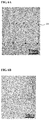
- FIGS. 6A and 6B are photographs illustrating the presence or absence of residual impurities in a sacrificial layer for use in an example and a comparison example that are classified according to layer structures of the sacrificial layer of a panel for a flexible digital X-ray detector.
- FIG. 7 is a flowchart of a method for manufacturing a panel for a flexible digital X-ray detector according to an embodiment of the present disclosure.
- FIG. 2 is a schematic plan view illustrating a digital X-ray detector.
- the digital X-ray detector may include a thin film transistor (TFT) array 110 , a gate driver 130 , a bias supplier 140 , a power-supply voltage supplier 150 , a readout circuit 160 , and a timing controller 170 .
- TFT thin film transistor
- the TFT array 110 may sense X-rays emitted from an energy source, may perform photoelectric conversion of the sensed signal, and may thus output an electrical detection signal.
- each cell region may be defined not only by a plurality of gate lines (GL) arranged in a horizontal direction, but also by a plurality of data lines (DL) arranged in a vertical direction perpendicular to the horizontal direction.
- Each cell region of the TFT array 110 may include a plurality of photosensitive pixels (P) arranged in a matrix.
- Each photosensitive pixel may include a PIN diode configured to sense light converted from X-rays and output the sensed light as a signal, and a thin film transistor (TFT) configured to transmit a detection signal output from the PIN diode in response to a gate signal.
- PIN diode configured to sense light converted from X-rays and output the sensed light as a signal
- TFT thin film transistor
- One side of the PIN diode may be connected to the thin film transistor (TFT), and the other side thereof may be connected to a bias line (BL).
- a gate electrode of the thin film transistor may be connected to the gate line (GL) through which a scan signal is transmitted, a source electrode may be connected to the PIN diode, and a drain electrode may be connected to the data line (DL) through which the detection signal is transmitted.
- the bias line BL may be arranged parallel to the data line (DL).
- the gate driver 130 may sequentially apply a plurality of gate signals, each of which has a gate-ON voltage level, through the gate lines (GL).
- the gate driver 130 may also apply a plurality of reset signals, each of which has a gate-ON voltage level, through a plurality of reset lines (RL).
- the gate-ON voltage level may refer to a voltage level at which thin film transistors of the photosensitive pixels can be turned on.
- the thin film transistors of the photosensitive pixels may be turned on in response to a gate signal or a reset signal.
- the gate driver 130 may be an integrated circuit (IC) such that the gate driver 130 may be populated on an external substrate connected to the TFT array 110 or may be formed over the TFT array 110 through a Gate In Panel (GIP) process.
- IC integrated circuit
- GIP Gate In Panel
- the bias supplier 140 may apply a drive voltage through bias lines (BL).
- the bias supplier 140 may apply a predetermined voltage to the PIN diode.
- the bias supplier 140 may selectively apply a reverse bias or a forward bias to the PIN diode.
- the power-supply voltage supplier 150 may supply a power-supply voltage to the photosensitive pixels through power-supply voltage lines (VL).
- VL power-supply voltage lines
- the readout circuit 160 may read out the detection signal generated from the thin film transistor (TFT) that is turned on in response to the gate signal. Accordingly, the detection signal generated from the PIN diode may be input to the readout circuit 160 through the data lines (DL).
- TFT thin film transistor
- the readout circuit 160 may include a signal detector, a multiplexer, etc.
- the signal detector may include a plurality of amplification circuits corresponding to the data lines (DL) on a one to one basis, and each amplification circuit may include an amplifier, a capacitor, a reset element, etc.
- the timing controller 170 may generate a start signal (STV), a clock signal (CPV), etc., and may transmit the start signal (STV), the clock signal (CPV), etc. to the gate driver 130 .
- the timing controller 170 may generate a readout control signal (ROC), a readout clock signal (CLK), etc., and may transmit the readout control signal (ROC), the readout clock signal (CLK), etc. to the readout circuit 160 .
- a panel for a digital X-ray detector according to one embodiment of the present disclosure will hereinafter be described with reference to FIGS. 2, 3 and 4 .
- a panel 200 for a flexible digital X-ray detector 200 may include multiple buffer layers (hereinafter referred to as a multi-buffer layer or a multiple layered buffer stack) 210 in which a silicon oxide (SiO x ) layer and a silicon nitride (SiN x ) layer are alternately stacked, a device array layer 220 that is disposed over the multi-buffer layer 210 and has a thin film transistor 230 and a PIN diode 240 connected to the thin film transistor 230 (e.g., see FIG. 4 ), and a scintillator layer 260 disposed over the device array layer 220 .
- multiple buffer layers hereinafter referred to as a multi-buffer layer or a multiple layered buffer stack
- SiO x silicon oxide
- SiN x silicon nitride
- the multi-buffer layer 210 serving as the lowest layer of the panel 200 may be disposed such that the SiO x layers and the SiN x layers are alternately stacked to form at least three layers.
- the SiO x layers and the SiN x layers may be alternately stacked in the form of various buffer layers, for example, SiO x /SiN x /SiO x , SiN x /SiO x /SiN x , SiO x /SiN x /SiO x /SiN x , SiN x /SiO x /SiN x /SiO x , etc.
- the panel 200 for the flexible digital X-ray detector does not have a base substrate, and the multi-buffer layer 210 forms the lowest layer of the panel 200 , such that the entire thickness of the panel 200 is reduced and flexibility can be more effectively allocated to the panel 200 .
- the multi-buffer layer 210 forms the lowest layer of the panel 200 , such that the multi-buffer layer 210 does not have a separate base substrate. As a result, device deterioration capable of being additionally generated by the base substrate during X-ray emission can be reduced.
- a threshold voltage of a device such as a thin film transistor (TFT) undergoes a negative shift when the device is exposed to X-rays.
- TFT thin film transistor
- a separate base substrate such as a glass substrate or a polyimide (PI) substrate is arranged in the digital X-ray detector, carrier variation of the thin film transistor occurs during X-ray emission, such that the additional threshold-voltage negative shift phenomenon occurs during X-ray emission, and thus device deterioration becomes more serious.
- the negative shift phenomenon caused by the PI substrate is about two or more times greater than the negative shift phenomenon caused by the glass substrate. Therefore, the panel 200 for the flexible digital X-ray detector in which the base substrate is removed and the multi-buffer layer 210 forms the lowest layer of the panel 200 may have flexibility and may reduce device deterioration.
- the thin film transistor 230 or the PIN diode 240 included in the device array layer 220 may be vulnerable to external moisture or oxygen penetration.
- the panel 200 according to the present disclosure includes a multi-buffer layer 210 in which the SiO x layer and the SiN x layer are alternatively stacked to form at least three layers in the lowest layer, instead of including a single buffer layer in the lowest layer, such that devices of the device array layer can be minimally affected by external moisture and oxygen penetration.
- the thin film transistor 230 and the device array layer 220 including the PIN diode 240 connected to the thin film transistor 230 may be disposed over the multi-buffer layer 210 .
- a pad part 290 including various lines may be disposed at the edge of the multi-buffer layer 210 , and the device array layer 220 may be formed in a manner that spacing of the edge of the multi-buffer layer 210 remains.
- pixel regions P may be defined by intersection regions of the gate lines GL arranged in one direction and the data lines DL arranged in the other direction perpendicular to the gate lines GL, and each of the pixel regions may include a thin film transistor 230 and a PIN diode 240 .
- the thin film transistor 230 may include an active layer 231 , a gate electrode 233 , a source electrode 235 , and a drain electrode 237 .
- the active layer 231 may be formed of an oxide semiconductor material such as indium gallium zinc oxide (IGZO), Low Temperature Polycrystalline Silicon (LTPS), or amorphous silicon (a-Si).
- the thin film transistor 230 may be connected to the PIN diode 240 that includes a lower electrode 241 , a PIN layer 243 , and an upper electrode 245 .
- the lower electrode 241 may be connected to the source electrode 235 of the thin film transistor 230 .
- the PIN layer 243 in which an N-type (negative) semiconductor layer having N-type impurities, an intrinsic (I-type) semiconductor layer having no impurities, and a P-type (positive) semiconductor layer including P-type impurities are sequentially stacked, may be formed.
- the PIN layer 243 may include a material capable of converting X-rays emitted from an energy source into an electric signal.
- the PIN layer 243 may include amorphous selenium (a-Se), mercuric iodide (HgI2), cadmium telluride (CdTe), lead oxide (PbO), lead iodide (PbI2), bismuth triiodide (BiI3), gallium arsenide (GaAs), germanium (Ge), and the like.
- the upper electrode 245 of the PIN diode may be connected to the bias electrode 247 through which a voltage is applied to the PIN diode 240 .
- a passivation layer 249 may be a monolayer or multilayer structure formed of a silicon oxide (SiOx) film or a silicon nitride (SiNx) film. The passivation layer 249 may be formed over the bias electrode 247 . In this case, the passivation layer 249 may be disposed to cover the entire surface of the device array layer 220 other than a contact hole of the bias electrode 247 , thereby protecting the device array layer 220 .
- the internal structure of the above-mentioned device array layer 220 is merely exemplary, and the scope or spirit of the present disclosure is not limited thereto.
- the arrangement format of various devices for example, the thin film transistor 230 , the PIN diode 240 , and the bias electrode 247 may include various modified examples.
- An organic layer 250 may be disposed over the device array layer 220 .
- the organic layer 250 may reduce a step difference caused by arrangement of the devices included in the device array layer 220 , and may be used as a planarization layer such that the scintillator layer 260 disposed at an upper part can be formed at the planarized surface.
- the organic layer 250 may serve as a growth base layer such that the scintillator can be formed as a plurality of columnar crystals (CC) 261 on the basis of the organic layer 250 .
- CC columnar crystals
- the panel 200 for the flexible digital X-ray detector may allow the scintillator layer 260 to be disposed over the device array layer 220 without formation of a separate adhesive layer.
- the scintillator layer 260 may be grown in the vertical direction in a manner that the scintillator layer 260 has a plurality of columnar crystals (CC) 261 through deposition by using the organic layer 250 as a growth base layer between the device array layer 220 and the scintillator layer 260 , such that the plurality of scintillator columnar crystals (CCs) may be arranged in parallel.
- the scintillator is formed of cesium iodide (CsI), the scope or spirit of the present disclosure is not limited thereto.
- the panel 200 according to the present disclosure can form the scintillator layer 260 over the device array layer 220 without having a separate adhesive layer, such that the entire thickness of the panel 200 can be greatly reduced, and more effective flexibility can be given to the panel 200 .
- the scintillator layer 260 may serve as a support substrate to provide rigidity to maintain the overall shape of the panel 200 .
- the embodiments of the present disclosure can remove the base substrate from the panel and use the lowest layer of the panel 200 as the multi-buffer layer 210 such that the panel has increased flexibility and the possibility of additional device deterioration is reduced.
- the scintillator layer 260 may serve as a support substrate to provide rigidity through which the scintillator layer 260 has flexibility and the entire shape of the panel 200 is maintained.
- the base substrate is reduced in thickness such that flexibility can be more effectively given to the panel 200 .
- a protective layer 270 may be formed to cover the scintillator layer 260 and the device array layer 220 at the scintillator layer 260 , such that the scintillator layer 260 may be formed to have stronger supporting force.
- the protective layer 270 may be formed of parylene.
- the protective layer 270 may be formed to cover the scintillators arranged in the plurality of columnar crystals (CCs) 261 , and may also be formed to bury spaces between the neighboring CCs 261 .
- a reflective layer 280 covering the protective layer 270 may be additionally disposed over the protective layer 270 , and may prevent light from leaking outside.
- the protective layer 270 and the reflective layer 280 may be disposed to cover the entire surface of the multi-buffer layer 210 other than the pad part 290 disposed at the edge of the device array layer 220 .
- the panel 200 for the above-mentioned flexible digital X-ray detector may operate as follows.
- X-rays emitted towards and received by the flexible digital X-ray detector panel 200 may be converted into visible light by the scintillator layer 260 .
- the visible light may be converted into an electronic signal by the PIN layer 243 of the PIN diode 240 .
- the intrinsic semiconductor layer when visible light is emitted towards and received by the PIN layer 243 , the intrinsic semiconductor layer is depleted by the P-type semiconductor layer and the N-type semiconductor layer, and thus generates an electric field therein. Electrons and holes generated by light may be drifted by the electric field, and are then collected in the P-type semiconductor layer and in the N-type semiconductor layer, respectively.
- the PIN diode 240 may convert visible light into an electronic signal, and may deliver the electronic signal to the thin film transistor 230 .
- the delivered electronic signal may be displayed as an image signal after passing through the data line DL connected to the thin film transistor 230 .
- FIGS. 5A to 5E illustrate a method for manufacturing a panel for a flexible digital X-ray detector according to an embodiment of the present disclosure
- FIG. 7 is a flowchart of a method for manufacturing a panel for a flexible digital X-ray detector according to an embodiment of the present disclosure.
- a method for manufacturing the panel according to the embodiment of the present disclosure will hereinafter be described with reference to FIGS. 5A to 5E and with reference to FIG. 7 .
- a method for manufacturing the panel 200 of the flexible digital X-ray detector may include forming 710 a sacrificial layer 320 over a sacrificial substrate 310 , forming 720 a multi-buffer layer 210 in which the SiO x layer and the SiN x layer are alternately stacked over the sacrificial layer 320 , forming 730 a device array layer 220 having a thin film transistor 230 and a PIN diode 240 connected to the thin film transistor 230 over the multi-buffer layer 210 , forming 740 a scintillator layer 260 over the device array layer 220 , and separating 750 the sacrificial layer 320 and the multi-buffer layer 210 .
- the sacrificial substrate 310 may be a region that will be isolated and removed by the next process such as laser lift off (LLO) in a subsequent process, and may serve as a base substrate for forming the sacrificial layer 320 , the multi-buffer layer 210 , and the device array layers 220 .
- the glass substrate may be used as a sacrificial substrate 310 .
- a sacrificial layer 320 which includes the amorphous silicon (a-Si) layer and the SiN x layer disposed at both sides of the amorphous silicon (a-Si) layer, may be disposed over the sacrificial substrate 310 .
- the respective layers may be formed using a common deposition method, and the formation method is not specially limited thereto.
- the multi-buffer layer 210 in which the SiO x layer and the SiN x layer are alternately stacked to form at least three layers may be formed over the sacrificial layer 320 .
- the device array layer 220 including the thin film transistor 230 and the PIN diode 240 connected to the thin film transistor 230 may be formed over the multi-buffer layer 210 , and the pad part 290 may be formed at the edge region of the multi-buffer layer 210 .
- the arrangement format of the thin film transistor 230 and the PIN diode 240 included in the device array layer 220 has various modified examples, without being limited to a specific structure, and a detailed description thereof will herein be omitted for convenience of description.
- An organic layer 250 for planarizing the device array layer 220 may be formed over the device array layer 220 .
- a plurality of CC (Columnar Crystal)-shaped scintillators may be grown through deposition on the organic layer 250 such that the CC-shaped scintillators can be vertically arranged in parallel, resulting in formation of the scintillator layer 260 .
- the organic layer 250 may also serve as a growth base layer for growing the scintillator columnar crystals (CCs) 261 .
- the protective layer 270 and the reflective layer 280 may be formed over the scintillator layer 260 , thereby covering the columnar crystals (CCs) 261 and the device array layer 220 .
- the interface between the sacrificial layer 320 and the multi-buffer layer 210 is isolated such that the sacrificial substrate 310 and the sacrificial layer 320 are removed.
- the panel 200 for the flexible digital X-ray detector according to the embodiment of the present disclosure can be obtained.
- the process for isolating the interface according to the present disclosure may be performed by the LLO process, and a detailed description thereof will hereinafter be given in detail.
- the LLO process refers to a process for using amplified laser to isolate device layers stacked on the sacrificial substrate 310 from the sacrificial substrate 310 .
- laser light is emitted towards and received by the sacrificial substrate 310 , and the interfacial bonding between the sacrificial layers 320 of the sacrificial substrate 310 and the device layers is destroyed, such that the sacrificial layers 320 and the device layers can be isolated from one another.
- the sacrificial layer 320 may be formed of the amorphous silicon (a-Si) material.
- hydrogen swelling occurs between the polyimide (PI) layer acting as an organic layer and the sacrificial layer 320 during laser emission, such that the sacrificial substrate 310 can be isolated.
- the hydrogen (H) content at the interface may be important to the LLO process.
- the present disclosure may not use a separate base substrate, and can use the multi-buffer layer 210 of the inorganic film as the lowest layer, such that there is a need to increase the hydrogen content at the interface.
- the SiN x layer having a high hydrogen content is disposed at both sides of the amorphous silicon (a-Si) layer, such that the hydrogen content of the sacrificial layer 320 is increased.
- the hydrogen content at the interface between the sacrificial layer 320 and the multi-buffer layer 210 increases, such that the sacrificial substrate 310 and the sacrificial layer 320 can be easily isolated from each other by the LLO process even when a separate base substrate is not used.
- the embodiment of the present disclosure does not form a separate base substrate at the lower part of the multi-buffer layer 210 so as to reduce additional device deterioration as well as to increase flexibility, such that the multi-buffer layer 210 composed of at least three layers may be formed below the device array layer 220 .
- the multi-buffer layer composed of at least three layers can allow the device array layer 220 to be minimally affected by laser light during LLO processing.
- FIG. 6A is a photograph illustrating the presence or absence of residual impurities for use in a comparison example in which a sacrificial layer is formed of amorphous silicon (a-Si) only
- FIG. 6B is a photograph illustrating the presence or absence of residual impurities for use in an example in which the LLO (laser lift off) process is performed in the embodiment based on a sacrificial layer.
- LLO laser lift off
- FIG. 6A illustrates a comparison example for a case in which the sacrificial layer is formed of the amorphous silicon (a-Si) material only
- FIG. 6B illustrates an example of a case in which the sacrificial layer is formed by arranging silicon nitride (SiNx) at both surfaces of the amorphous silicon (a-Si) layer such that the sacrificial layer is isolated from the multi-buffer layer through laser lift off (LLO) processing according to an embodiment of the present disclosure.
- SiNx silicon nitride
- the operation for removing and isolating the sacrificial layer using laser light is not completely performed, such that a large amount of residual impurities formed of amorphous silicon (a-Si) remains (e.g., see impurity 610 ).
- the silicon nitride (SiNx) layer having a high hydrogen content is disposed at both surfaces of the amorphous silicon (a-Si) layer, hydrogen swelling occurs in the SiN x layer due to laser light, and the sacrificial layer can be sufficiently removed and isolated from the multi-buffer layer, such that it can be confirmed that hardly any residual impurities remain.
- the embodiments of the present disclosure may reduce device deterioration caused by a base substrate during X-ray emission because the lowest layer of a panel is composed of multiple buffer layers without having a separate base substrate.
- the embodiments of the present disclosure may allow a scintillator layer to serve as a support substrate that is capable of providing rigidity to maintain the shape of a panel without using a separate base substrate and the junction between the device layer and the scintillator layer can be formed without and adhesive layer, such that a total thickness of the panel is reduced and the panel has increased flexibility.
- the embodiments of the present disclosure may use a sacrificial layer that includes an amorphous silicon (a-Si) layer and a silicon nitride (SiNx) layer disposed at both surfaces of the amorphous silicon (a-Si) layer during LLO (Laser Lift Off) processing, may effectively isolate a sacrificial layer from a sacrificial substrate by increasing hydrogen content at an interface, and may reduce the amount of residual impurities remaining in the sacrificial layer after isolation between the sacrificial layer and the sacrificial substrate.
- a-Si amorphous silicon
- SiNx silicon nitride
Landscapes
- Health & Medical Sciences (AREA)
- Physics & Mathematics (AREA)
- General Physics & Mathematics (AREA)
- Life Sciences & Earth Sciences (AREA)
- Spectroscopy & Molecular Physics (AREA)
- Molecular Biology (AREA)
- High Energy & Nuclear Physics (AREA)
- General Health & Medical Sciences (AREA)
- Engineering & Computer Science (AREA)
- Medical Informatics (AREA)
- Optics & Photonics (AREA)
- Nuclear Medicine, Radiotherapy & Molecular Imaging (AREA)
- Biomedical Technology (AREA)
- Chemical & Material Sciences (AREA)
- Crystallography & Structural Chemistry (AREA)
- Biochemistry (AREA)
- Analytical Chemistry (AREA)
- Immunology (AREA)
- Pathology (AREA)
- Measurement Of Radiation (AREA)
- Solid State Image Pick-Up Elements (AREA)
- Materials Engineering (AREA)
- Nanotechnology (AREA)
Abstract
Description
Claims (18)
Applications Claiming Priority (2)
| Application Number | Priority Date | Filing Date | Title |
|---|---|---|---|
| KR10-2017-0170777 | 2017-12-12 | ||
| KR1020170170777A KR102466811B1 (en) | 2017-12-12 | 2017-12-12 | Flexible digital x-ray detector panel and the manufacturing method thereof |
Publications (2)
| Publication Number | Publication Date |
|---|---|
| US20190179039A1 US20190179039A1 (en) | 2019-06-13 |
| US10852447B2 true US10852447B2 (en) | 2020-12-01 |
Family
ID=66696707
Family Applications (1)
| Application Number | Title | Priority Date | Filing Date |
|---|---|---|---|
| US16/211,107 Active 2039-01-17 US10852447B2 (en) | 2017-12-12 | 2018-12-05 | Panel for flexible digital x-ray detector and method for manufacturing the same |
Country Status (3)
| Country | Link |
|---|---|
| US (1) | US10852447B2 (en) |
| KR (1) | KR102466811B1 (en) |
| CN (1) | CN110034137B (en) |
Families Citing this family (9)
| Publication number | Priority date | Publication date | Assignee | Title |
|---|---|---|---|---|
| US10921467B2 (en) * | 2017-09-15 | 2021-02-16 | Analogic Corporation | Detector array for imaging modality |
| KR102722127B1 (en) * | 2018-10-18 | 2024-10-24 | 엘지디스플레이 주식회사 | Thin film transistor array substrate for high resolution digital x-ray detector and the high resolution digital x-ray detector including the same |
| CN112713155B (en) * | 2019-10-25 | 2025-11-04 | 睿生光电股份有限公司 | Electronic devices |
| JP7337663B2 (en) * | 2019-10-30 | 2023-09-04 | キヤノン株式会社 | Method for manufacturing radiation detection device |
| US11251210B2 (en) * | 2020-02-07 | 2022-02-15 | Sensors Unlimited, Inc. | Pin diodes with over-current protection |
| EP3876280A1 (en) | 2020-03-05 | 2021-09-08 | Nederlandse Organisatie voor toegepast- natuurwetenschappelijk Onderzoek TNO | Process of manufacturing an x-ray imaging device and to an x-ray imaging device produced by such a process |
| CN113811998B (en) * | 2020-04-17 | 2024-02-20 | 京东方科技集团股份有限公司 | Flat panel detector substrate and manufacturing method thereof, flat panel detector |
| CN113410258B (en) * | 2021-06-18 | 2022-12-16 | 福州京东方光电科技有限公司 | A detection substrate and a detection device |
| CN121398163A (en) * | 2024-07-17 | 2026-01-23 | 北京京东方传感技术有限公司 | Photoelectric conversion substrate and flat panel inspection device |
Citations (9)
| Publication number | Priority date | Publication date | Assignee | Title |
|---|---|---|---|---|
| US20090202743A1 (en) * | 2003-05-15 | 2009-08-13 | General Electric Company | Multilayer coating package on flexible substrates for electro-optical devices |
| US20100207033A1 (en) * | 2009-02-18 | 2010-08-19 | Yu-Cheng Chen | X-ray detector and fabrication method thereof |
| US20110198505A1 (en) * | 2010-02-18 | 2011-08-18 | Canon Kabushiki Kaisha | Radiation detector and radiation detection system |
| US20150144889A1 (en) * | 2013-11-22 | 2015-05-28 | General Electric Company | Organic x-ray detector with barrier layer |
| US20150164447A1 (en) * | 2013-12-17 | 2015-06-18 | General Electric Company | Method and system for integrated medical transport backboard digital x-ray imaging detector |
| US20160013243A1 (en) * | 2014-03-10 | 2016-01-14 | Dpix, Llc | Photosensor arrays for detection of radiation and process for the preparation thereof |
| US20180102393A1 (en) * | 2016-10-12 | 2018-04-12 | Innolux Corporation | Photo detector device |
| US20190079201A1 (en) * | 2017-09-12 | 2019-03-14 | Palo Alto Research Center Incorporated | Monolithic digital x-ray detector stack with energy resolution |
| US20190333961A1 (en) * | 2017-01-06 | 2019-10-31 | Carestream Health, Inc. | Detach and reattach of a flexible polyimide based x-ray detector |
Family Cites Families (17)
| Publication number | Priority date | Publication date | Assignee | Title |
|---|---|---|---|---|
| US7078702B2 (en) * | 2002-07-25 | 2006-07-18 | General Electric Company | Imager |
| WO2005038490A1 (en) * | 2003-10-22 | 2005-04-28 | Canon Kabushiki Kaisha | Radiation detection device, scintillator panel, method of making the same, making apparatus, and radiation image pick-up system |
| KR101350795B1 (en) * | 2007-06-11 | 2014-01-10 | 삼성디스플레이 주식회사 | Thin film transistor array substrate for x-ray detector |
| US8569704B2 (en) * | 2010-12-21 | 2013-10-29 | Carestream Health, Inc. | Digital radiographic detector array including spacers and methods for same |
| JP5728250B2 (en) * | 2011-03-01 | 2015-06-03 | キヤノン株式会社 | Radiation detection apparatus, scintillator panel, manufacturing method thereof, and radiation detection system |
| WO2013157231A1 (en) * | 2012-04-17 | 2013-10-24 | 株式会社 東芝 | Method for manufacturing x-ray planar detector, and tft array substrate for x-ray planar detector |
| KR101971111B1 (en) * | 2012-09-11 | 2019-04-23 | 삼성디스플레이 주식회사 | Apparatus for detecting X-ray |
| KR20140056670A (en) * | 2012-10-30 | 2014-05-12 | 삼성테크윈 주식회사 | X-ray detector and x-ray deting system |
| TWI496277B (en) * | 2012-12-03 | 2015-08-11 | Innocom Tech Shenzhen Co Ltd | X-ray detection device |
| KR102071330B1 (en) * | 2012-12-27 | 2020-01-30 | 엘지디스플레이 주식회사 | Organic light emitting display device and method for manufacturing the same |
| CN103268891B (en) * | 2013-03-28 | 2016-08-10 | 北京京东方光电科技有限公司 | A kind of thin film transistor (TFT), amorphous silicon flat panel detection substrate and preparation method |
| KR102090710B1 (en) * | 2013-06-26 | 2020-03-19 | 삼성디스플레이 주식회사 | Thin film transistor substrate, organic light emitting apparatus comprising the same, method for manufacturing thin film transistor substrate, and method for manufacturing organic light emitting apparatus |
| KR102175353B1 (en) * | 2014-05-30 | 2020-11-09 | 한국전자통신연구원 | A semiconductor device and method for fabricating the same |
| WO2016002562A1 (en) * | 2014-06-30 | 2016-01-07 | シャープ株式会社 | Imaging panel and x-ray imaging device |
| US9520437B2 (en) * | 2014-08-14 | 2016-12-13 | Cbrite Inc. | Flexible APS X-ray imager with MOTFT pixel readout and a pin diode sensing element |
| US10890669B2 (en) * | 2015-01-14 | 2021-01-12 | General Electric Company | Flexible X-ray detector and methods for fabricating the same |
| JP6485545B2 (en) * | 2015-06-24 | 2019-03-20 | 株式会社島津製作所 | Radiation detector and radiation imaging apparatus having the same |
-
2017
- 2017-12-12 KR KR1020170170777A patent/KR102466811B1/en active Active
-
2018
- 2018-12-05 US US16/211,107 patent/US10852447B2/en active Active
- 2018-12-11 CN CN201811510773.9A patent/CN110034137B/en active Active
Patent Citations (9)
| Publication number | Priority date | Publication date | Assignee | Title |
|---|---|---|---|---|
| US20090202743A1 (en) * | 2003-05-15 | 2009-08-13 | General Electric Company | Multilayer coating package on flexible substrates for electro-optical devices |
| US20100207033A1 (en) * | 2009-02-18 | 2010-08-19 | Yu-Cheng Chen | X-ray detector and fabrication method thereof |
| US20110198505A1 (en) * | 2010-02-18 | 2011-08-18 | Canon Kabushiki Kaisha | Radiation detector and radiation detection system |
| US20150144889A1 (en) * | 2013-11-22 | 2015-05-28 | General Electric Company | Organic x-ray detector with barrier layer |
| US20150164447A1 (en) * | 2013-12-17 | 2015-06-18 | General Electric Company | Method and system for integrated medical transport backboard digital x-ray imaging detector |
| US20160013243A1 (en) * | 2014-03-10 | 2016-01-14 | Dpix, Llc | Photosensor arrays for detection of radiation and process for the preparation thereof |
| US20180102393A1 (en) * | 2016-10-12 | 2018-04-12 | Innolux Corporation | Photo detector device |
| US20190333961A1 (en) * | 2017-01-06 | 2019-10-31 | Carestream Health, Inc. | Detach and reattach of a flexible polyimide based x-ray detector |
| US20190079201A1 (en) * | 2017-09-12 | 2019-03-14 | Palo Alto Research Center Incorporated | Monolithic digital x-ray detector stack with energy resolution |
Also Published As
| Publication number | Publication date |
|---|---|
| CN110034137A (en) | 2019-07-19 |
| KR102466811B1 (en) | 2022-11-11 |
| US20190179039A1 (en) | 2019-06-13 |
| CN110034137B (en) | 2023-09-19 |
| KR20190070195A (en) | 2019-06-20 |
Similar Documents
| Publication | Publication Date | Title |
|---|---|---|
| US10852447B2 (en) | Panel for flexible digital x-ray detector and method for manufacturing the same | |
| US10811457B2 (en) | Array substrate for digital x-ray detector, digital x-ray detector including the same, and method for manufacturing the same | |
| US11296139B2 (en) | Array substrate for digital X-ray detector and X-ray detector including the same | |
| US9520437B2 (en) | Flexible APS X-ray imager with MOTFT pixel readout and a pin diode sensing element | |
| US10707251B2 (en) | Array substrate for digital X-ray detector, and digital X-ray detector including the same | |
| US10386503B2 (en) | Array substrate for digital X-ray detector, digital X-ray detector including the same, and method for manufacturing the same | |
| US10795034B2 (en) | Digital X-ray detector panel and X-ray system including the same | |
| US11209557B2 (en) | Array substrate for digital X-ray detector, digital X-ray detector including the same, and method for manufacturing the same | |
| US10651227B2 (en) | Array substrate for X-ray detector and X-ray detector including the same | |
| US20120305777A1 (en) | Radiation image pickup device and radiation image pickup display system including the same | |
| KR102670831B1 (en) | Digital x-ray detector having light shielding layer and method of fabricating thereof | |
| JP2012247327A5 (en) | ||
| KR20180044681A (en) | Digital x-ray detector for improving read out efficiency and method for fabricationg thereof | |
| US11269089B2 (en) | Digital X-ray detector | |
| CN112992943B (en) | Thin film transistor array substrate and manufacturing method thereof and digital X-ray detector device | |
| KR20210071570A (en) | Thin film transistor array substrate for digital x-ray detector and the digital x-ray detector including the same | |
| JP2013156119A (en) | Radiation imaging apparatus, manufacturing method thereof, and radiation imaging display system | |
| KR102619971B1 (en) | Digital x-ray detector and method of fabricating thereof | |
| KR101858356B1 (en) | Digital x-ray detector for blocking hydrogen |
Legal Events
| Date | Code | Title | Description |
|---|---|---|---|
| FEPP | Fee payment procedure |
Free format text: ENTITY STATUS SET TO UNDISCOUNTED (ORIGINAL EVENT CODE: BIG.); ENTITY STATUS OF PATENT OWNER: LARGE ENTITY |
|
| AS | Assignment |
Owner name: LG DISPLAY CO., LTD., KOREA, REPUBLIC OF Free format text: ASSIGNMENT OF ASSIGNORS INTEREST;ASSIGNORS:KIM, JINPIL;YUN, MINSEOK;REEL/FRAME:047750/0165 Effective date: 20181129 |
|
| STPP | Information on status: patent application and granting procedure in general |
Free format text: DOCKETED NEW CASE - READY FOR EXAMINATION |
|
| STPP | Information on status: patent application and granting procedure in general |
Free format text: NON FINAL ACTION MAILED |
|
| STPP | Information on status: patent application and granting procedure in general |
Free format text: RESPONSE TO NON-FINAL OFFICE ACTION ENTERED AND FORWARDED TO EXAMINER |
|
| STPP | Information on status: patent application and granting procedure in general |
Free format text: PUBLICATIONS -- ISSUE FEE PAYMENT RECEIVED |
|
| STCF | Information on status: patent grant |
Free format text: PATENTED CASE |
|
| MAFP | Maintenance fee payment |
Free format text: PAYMENT OF MAINTENANCE FEE, 4TH YEAR, LARGE ENTITY (ORIGINAL EVENT CODE: M1551); ENTITY STATUS OF PATENT OWNER: LARGE ENTITY Year of fee payment: 4 |