US10804372B2 - Gate-all-around field effect transistor and method for manufacturing same - Google Patents
Gate-all-around field effect transistor and method for manufacturing same Download PDFInfo
- Publication number
- US10804372B2 US10804372B2 US16/181,630 US201816181630A US10804372B2 US 10804372 B2 US10804372 B2 US 10804372B2 US 201816181630 A US201816181630 A US 201816181630A US 10804372 B2 US10804372 B2 US 10804372B2
- Authority
- US
- United States
- Prior art keywords
- layer
- channel
- dummy gate
- spacer
- fin structure
- Prior art date
- Legal status (The legal status is an assumption and is not a legal conclusion. Google has not performed a legal analysis and makes no representation as to the accuracy of the status listed.)
- Active, expires
Links
Images


Classifications
-
- H01L29/66545—
-
- B—PERFORMING OPERATIONS; TRANSPORTING
- B82—NANOTECHNOLOGY
- B82Y—SPECIFIC USES OR APPLICATIONS OF NANOSTRUCTURES; MEASUREMENT OR ANALYSIS OF NANOSTRUCTURES; MANUFACTURE OR TREATMENT OF NANOSTRUCTURES
- B82Y10/00—Nanotechnology for information processing, storage or transmission, e.g. quantum computing or single electron logic
-
- H01L21/306—
-
- H01L29/0673—
-
- H01L29/0847—
-
- H01L29/4236—
-
- H01L29/42392—
-
- H01L29/66439—
-
- H01L29/6656—
-
- H01L29/66742—
-
- H01L29/66772—
-
- H01L29/6681—
-
- H01L29/785—
-
- H01L29/78654—
-
- H01L29/78696—
-
- H—ELECTRICITY
- H10—SEMICONDUCTOR DEVICES; ELECTRIC SOLID-STATE DEVICES NOT OTHERWISE PROVIDED FOR
- H10D—INORGANIC ELECTRIC SEMICONDUCTOR DEVICES
- H10D30/00—Field-effect transistors [FET]
- H10D30/01—Manufacture or treatment
- H10D30/014—Manufacture or treatment of FETs having zero-dimensional [0D] or one-dimensional [1D] channels, e.g. quantum wire FETs, single-electron transistors [SET] or Coulomb blockade transistors
-
- H—ELECTRICITY
- H10—SEMICONDUCTOR DEVICES; ELECTRIC SOLID-STATE DEVICES NOT OTHERWISE PROVIDED FOR
- H10D—INORGANIC ELECTRIC SEMICONDUCTOR DEVICES
- H10D30/00—Field-effect transistors [FET]
- H10D30/01—Manufacture or treatment
- H10D30/021—Manufacture or treatment of FETs having insulated gates [IGFET]
- H10D30/024—Manufacture or treatment of FETs having insulated gates [IGFET] of fin field-effect transistors [FinFET]
- H10D30/0243—Manufacture or treatment of FETs having insulated gates [IGFET] of fin field-effect transistors [FinFET] using dummy structures having essentially the same shapes as the semiconductor bodies, e.g. to provide stability
-
- H—ELECTRICITY
- H10—SEMICONDUCTOR DEVICES; ELECTRIC SOLID-STATE DEVICES NOT OTHERWISE PROVIDED FOR
- H10D—INORGANIC ELECTRIC SEMICONDUCTOR DEVICES
- H10D30/00—Field-effect transistors [FET]
- H10D30/01—Manufacture or treatment
- H10D30/021—Manufacture or treatment of FETs having insulated gates [IGFET]
- H10D30/031—Manufacture or treatment of FETs having insulated gates [IGFET] of thin-film transistors [TFT]
- H10D30/0321—Manufacture or treatment of FETs having insulated gates [IGFET] of thin-film transistors [TFT] comprising silicon, e.g. amorphous silicon or polysilicon
- H10D30/0323—Manufacture or treatment of FETs having insulated gates [IGFET] of thin-film transistors [TFT] comprising silicon, e.g. amorphous silicon or polysilicon comprising monocrystalline silicon
-
- H—ELECTRICITY
- H10—SEMICONDUCTOR DEVICES; ELECTRIC SOLID-STATE DEVICES NOT OTHERWISE PROVIDED FOR
- H10D—INORGANIC ELECTRIC SEMICONDUCTOR DEVICES
- H10D30/00—Field-effect transistors [FET]
- H10D30/40—FETs having zero-dimensional [0D], one-dimensional [1D] or two-dimensional [2D] charge carrier gas channels
- H10D30/43—FETs having zero-dimensional [0D], one-dimensional [1D] or two-dimensional [2D] charge carrier gas channels having one-dimensional [1D] charge carrier gas channels, e.g. quantum wire FETs or transistors having 1D quantum-confined channels
-
- H—ELECTRICITY
- H10—SEMICONDUCTOR DEVICES; ELECTRIC SOLID-STATE DEVICES NOT OTHERWISE PROVIDED FOR
- H10D—INORGANIC ELECTRIC SEMICONDUCTOR DEVICES
- H10D30/00—Field-effect transistors [FET]
- H10D30/60—Insulated-gate field-effect transistors [IGFET]
- H10D30/62—Fin field-effect transistors [FinFET]
- H10D30/6215—Fin field-effect transistors [FinFET] having multiple independently-addressable gate electrodes
-
- H—ELECTRICITY
- H10—SEMICONDUCTOR DEVICES; ELECTRIC SOLID-STATE DEVICES NOT OTHERWISE PROVIDED FOR
- H10D—INORGANIC ELECTRIC SEMICONDUCTOR DEVICES
- H10D30/00—Field-effect transistors [FET]
- H10D30/60—Insulated-gate field-effect transistors [IGFET]
- H10D30/67—Thin-film transistors [TFT]
- H10D30/6729—Thin-film transistors [TFT] characterised by the electrodes
- H10D30/673—Thin-film transistors [TFT] characterised by the electrodes characterised by the shapes, relative sizes or dispositions of the gate electrodes
- H10D30/6735—Thin-film transistors [TFT] characterised by the electrodes characterised by the shapes, relative sizes or dispositions of the gate electrodes having gates fully surrounding the channels, e.g. gate-all-around
-
- H—ELECTRICITY
- H10—SEMICONDUCTOR DEVICES; ELECTRIC SOLID-STATE DEVICES NOT OTHERWISE PROVIDED FOR
- H10D—INORGANIC ELECTRIC SEMICONDUCTOR DEVICES
- H10D30/00—Field-effect transistors [FET]
- H10D30/60—Insulated-gate field-effect transistors [IGFET]
- H10D30/67—Thin-film transistors [TFT]
- H10D30/674—Thin-film transistors [TFT] characterised by the active materials
- H10D30/6741—Group IV materials, e.g. germanium or silicon carbide
- H10D30/6743—Silicon
- H10D30/6744—Monocrystalline silicon
-
- H—ELECTRICITY
- H10—SEMICONDUCTOR DEVICES; ELECTRIC SOLID-STATE DEVICES NOT OTHERWISE PROVIDED FOR
- H10D—INORGANIC ELECTRIC SEMICONDUCTOR DEVICES
- H10D30/00—Field-effect transistors [FET]
- H10D30/60—Insulated-gate field-effect transistors [IGFET]
- H10D30/67—Thin-film transistors [TFT]
- H10D30/6757—Thin-film transistors [TFT] characterised by the structure of the channel, e.g. transverse or longitudinal shape or doping profile
-
- H—ELECTRICITY
- H10—SEMICONDUCTOR DEVICES; ELECTRIC SOLID-STATE DEVICES NOT OTHERWISE PROVIDED FOR
- H10D—INORGANIC ELECTRIC SEMICONDUCTOR DEVICES
- H10D62/00—Semiconductor bodies, or regions thereof, of devices having potential barriers
- H10D62/10—Shapes, relative sizes or dispositions of the regions of the semiconductor bodies; Shapes of the semiconductor bodies
- H10D62/113—Isolations within a component, i.e. internal isolations
- H10D62/115—Dielectric isolations, e.g. air gaps
- H10D62/116—Dielectric isolations, e.g. air gaps adjoining the input or output regions of field-effect devices, e.g. adjoining source or drain regions
-
- H—ELECTRICITY
- H10—SEMICONDUCTOR DEVICES; ELECTRIC SOLID-STATE DEVICES NOT OTHERWISE PROVIDED FOR
- H10D—INORGANIC ELECTRIC SEMICONDUCTOR DEVICES
- H10D62/00—Semiconductor bodies, or regions thereof, of devices having potential barriers
- H10D62/10—Shapes, relative sizes or dispositions of the regions of the semiconductor bodies; Shapes of the semiconductor bodies
- H10D62/117—Shapes of semiconductor bodies
- H10D62/118—Nanostructure semiconductor bodies
- H10D62/119—Nanowire, nanosheet or nanotube semiconductor bodies
- H10D62/121—Nanowire, nanosheet or nanotube semiconductor bodies oriented parallel to substrates
-
- H—ELECTRICITY
- H10—SEMICONDUCTOR DEVICES; ELECTRIC SOLID-STATE DEVICES NOT OTHERWISE PROVIDED FOR
- H10D—INORGANIC ELECTRIC SEMICONDUCTOR DEVICES
- H10D62/00—Semiconductor bodies, or regions thereof, of devices having potential barriers
- H10D62/10—Shapes, relative sizes or dispositions of the regions of the semiconductor bodies; Shapes of the semiconductor bodies
- H10D62/13—Semiconductor regions connected to electrodes carrying current to be rectified, amplified or switched, e.g. source or drain regions
- H10D62/149—Source or drain regions of field-effect devices
- H10D62/151—Source or drain regions of field-effect devices of IGFETs
-
- H—ELECTRICITY
- H10—SEMICONDUCTOR DEVICES; ELECTRIC SOLID-STATE DEVICES NOT OTHERWISE PROVIDED FOR
- H10D—INORGANIC ELECTRIC SEMICONDUCTOR DEVICES
- H10D64/00—Electrodes of devices having potential barriers
- H10D64/01—Manufacture or treatment
- H10D64/017—Manufacture or treatment using dummy gates in processes wherein at least parts of the final gates are self-aligned to the dummy gates, i.e. replacement gate processes
-
- H—ELECTRICITY
- H10—SEMICONDUCTOR DEVICES; ELECTRIC SOLID-STATE DEVICES NOT OTHERWISE PROVIDED FOR
- H10D—INORGANIC ELECTRIC SEMICONDUCTOR DEVICES
- H10D64/00—Electrodes of devices having potential barriers
- H10D64/01—Manufacture or treatment
- H10D64/021—Manufacture or treatment using multiple gate spacer layers, e.g. bilayered sidewall spacers
-
- H—ELECTRICITY
- H10—SEMICONDUCTOR DEVICES; ELECTRIC SOLID-STATE DEVICES NOT OTHERWISE PROVIDED FOR
- H10D—INORGANIC ELECTRIC SEMICONDUCTOR DEVICES
- H10D64/00—Electrodes of devices having potential barriers
- H10D64/20—Electrodes characterised by their shapes, relative sizes or dispositions
- H10D64/27—Electrodes not carrying the current to be rectified, amplified, oscillated or switched, e.g. gates
- H10D64/311—Gate electrodes for field-effect devices
- H10D64/411—Gate electrodes for field-effect devices for FETs
- H10D64/511—Gate electrodes for field-effect devices for FETs for IGFETs
- H10D64/512—Disposition of the gate electrodes, e.g. buried gates
- H10D64/513—Disposition of the gate electrodes, e.g. buried gates within recesses in the substrate, e.g. trench gates, groove gates or buried gates
-
- H—ELECTRICITY
- H10—SEMICONDUCTOR DEVICES; ELECTRIC SOLID-STATE DEVICES NOT OTHERWISE PROVIDED FOR
- H10D—INORGANIC ELECTRIC SEMICONDUCTOR DEVICES
- H10D64/00—Electrodes of devices having potential barriers
- H10D64/20—Electrodes characterised by their shapes, relative sizes or dispositions
- H10D64/27—Electrodes not carrying the current to be rectified, amplified, oscillated or switched, e.g. gates
- H10D64/311—Gate electrodes for field-effect devices
- H10D64/411—Gate electrodes for field-effect devices for FETs
- H10D64/511—Gate electrodes for field-effect devices for FETs for IGFETs
- H10D64/514—Gate electrodes for field-effect devices for FETs for IGFETs characterised by the insulating layers
-
- H—ELECTRICITY
- H10—SEMICONDUCTOR DEVICES; ELECTRIC SOLID-STATE DEVICES NOT OTHERWISE PROVIDED FOR
- H10P—GENERIC PROCESSES OR APPARATUS FOR THE MANUFACTURE OR TREATMENT OF DEVICES COVERED BY CLASS H10
- H10P50/00—Etching of wafers, substrates or parts of devices
Definitions
- This application relates to the field of semiconductor technologies, and in particular, to a gate-all-around field effect transistor and a method for manufacturing the same.
- a solution to the foregoing problem is forming an internal spacer between the gate and the drain region and between the gate and the source region.
- existence of the internal spacer increases distances between the source region and the drain region that are formed by means of epitaxy and a channel. Consequently, a stress introduced into the channel is reduced, leading to on-state current reduction and device performance degradation of the gate-all-around field effect transistor.
- An objective of this application is to increase an on-state current of a gate-all-around field effect transistor.
- a method for manufacturing a gate-all-around field effect transistor may include: forming a first fin structure on a substrate, where the first fin structure includes one first laminated structure or a plurality of first laminated structures stacked, where the first laminated structure sequentially includes a sacrificial layer, a support layer, and a channel layer from bottom to top; forming a dummy gate structure across the first fin structure, where the dummy gate structure includes a dummy gate dielectric layer on a surface of the first fin structure, a dummy gate on the dummy gate dielectric layer, and a first spacer on a side surface of the dummy gate; removing parts of the first fin structure located on two sides of the dummy gate structure to form a second fin structure; performing first etching on a side surface of the sacrificial layer in the second fin structure to form a first space; forming a second spacer in the first space; performing second etching on a side
- forming a second spacer in the first space includes: after the first space is formed, depositing a second spacer material, where a part of the second spacer material fills the first space; and removing a part of the second spacer material other than the part of the second spacer material that fills the first space, and using the remaining second spacer material as the second spacer.
- the first fin structure further includes one second laminated structure or a plurality of second laminated structures stacked on the first laminated structure, where the second laminated structure sequentially includes the support layer, the sacrificial layer, the support layer, and the channel layer from bottom to top.
- the method further includes forming an inter-layer dielectric layer, where the inter-layer dielectric layer exposes the dummy gate; removing the dummy gate and the dummy gate dielectric layer to form a first trench; and removing the sacrificial layer and a part of the support layer located on the sacrificial layer in the second fin structure to form a second trench, so as to form the channel layer suspended above the substrate.
- a part of the support layer located above the second spacer is further removed.
- the method further includes: forming a gate dielectric layer on a bottom and a sidewall of the second trench and a surface of the channel layer; and after the gate dielectric layer is formed, filling the second trench with a gate.
- the channel layer includes a nanowire.
- the support layer and the sacrificial layer have different etching selectivity ratios; and the support layer and the channel layer have different etching selectivity ratios.
- materials of the sacrificial layer and the support layer include SiGe; and a material of the channel layer includes Si.
- the sacrificial layer and the support layer have different contents of Ge.
- a content of Ge in the sacrificial layer is greater than a content of Ge in the support layer.
- a content of Ge in the sacrificial layer is less than a content of Ge in the support layer.
- a gate-all-around field effect transistor may include: one channel layer or a plurality of channel layers separated from each other from bottom to top above a substrate; a gate structure all around the channel layer, where the gate structure sequentially includes a first gate dielectric layer and a gate from inside to outside; a source region and a drain region, located on two sides of the gate structure and formed by performing epitaxy on a side surface of the channel layer; a second gate dielectric layer, located between the gate and the source region and between the gate and the drain region; and a spacer, located between the second gate dielectric layer and the source region and between the second gate dielectric layer and the drain region, where along a direction of a channel, compared with a side surface, distal to the gate, of the spacer, the side surface of the channel layer is closer to the gate.
- the channel layer includes a nanowire.
- the field effect transistor further includes a third gate dielectric layer, located between an upper surface of the spacer and the source region and between the upper surface of the spacer and the drain region.
- the second spacer is formed so that parasitic capacitance can be reduced.
- the side surface of the channel layer after the second etching is closer to the sacrificial layer, so that the side surface of the channel layer is closer to the gate formed after the sacrificial layer is removed, thereby increasing an on-state current of a gate-all-around field effect transistor.
- FIG. 1 is a simplified flowchart of a method for manufacturing a gate-all-around field effect transistor
- FIG. 2A shows a schematic cross-sectional diagram along a direction of a channel of a stage of a method for manufacturing a gate-all-around field effect transistor
- FIG. 2B shows a schematic cross-sectional diagram along a direction perpendicular to the direction of the channel of the stage shown in FIG. 2A ;
- FIG. 3A shows a schematic cross-sectional diagram along a direction of a channel of a stage of a method for manufacturing a gate-all-around field effect transistor
- FIG. 3B shows a schematic cross-sectional diagram along a direction perpendicular to the direction of the channel of the stage shown in FIG. 3A ;
- FIG. 4A shows a schematic cross-sectional diagram along a direction of a channel of a stage of a method for manufacturing a gate-all-around field effect transistor
- FIG. 4B shows a schematic cross-sectional diagram along a direction perpendicular to the direction of the channel of the stage shown in FIG. 4A ;
- FIG. 5A shows a schematic cross-sectional diagram along a direction of a channel of a stage of a method for manufacturing a gate-all-around field effect transistor
- FIG. 5B shows a schematic cross-sectional diagram along a direction perpendicular to the direction of the channel of the stage shown in FIG. 5A ;
- FIG. 6A shows a schematic cross-sectional diagram along a direction of a channel of a stage of a method for manufacturing a gate-all-around field effect transistor
- FIG. 6B shows a schematic cross-sectional diagram along a direction perpendicular to the direction of the channel of the stage shown in FIG. 6A ;
- FIG. 7A shows a schematic cross-sectional diagram along a direction of a channel of a stage of a method for manufacturing a gate-all-around field effect transistor
- FIG. 7B shows a schematic cross-sectional diagram along a direction perpendicular to the direction of the channel of the stage shown in FIG. 7A ;
- FIG. 8A shows a schematic cross-sectional diagram along a direction of a channel of a stage of a method for manufacturing a gate-all-around field effect transistor
- FIG. 8B shows a schematic cross-sectional diagram along a direction perpendicular to the direction of the channel of the stage shown in FIG. 8A ;
- FIG. 9A shows a schematic cross-sectional diagram along a direction of a channel of a stage of a method for manufacturing a gate-all-around field effect transistor
- FIG. 9B shows a schematic cross-sectional diagram along a direction perpendicular to the direction of the channel of the stage shown in FIG. 9A ;
- FIG. 10A shows a schematic cross-sectional diagram along a direction of a channel of a stage of a method for manufacturing a gate-all-around field effect transistor
- FIG. 10B shows a schematic cross-sectional diagram along a direction perpendicular to the direction of the channel of the stage shown in FIG. 10A ;
- FIG. 11A shows a schematic cross-sectional diagram along a direction of a channel of a stage of a method for manufacturing a gate-all-around field effect transistor
- FIG. 11B shows a schematic cross-sectional diagram along a direction perpendicular to the direction of the channel of the stage shown in FIG. 11A ;
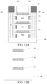
- FIG. 12A shows a schematic cross-sectional diagram along a direction of a channel of a stage of a method for manufacturing a gate-all-around field effect transistor
- FIG. 12B shows a schematic cross-sectional diagram along a direction perpendicular to the direction of the channel of the stage shown in FIG. 12A ;
- FIG. 13A shows a schematic cross-sectional diagram along a direction of a channel of a stage of a method for manufacturing a gate-all-around field effect transistor
- FIG. 13B shows a schematic cross-sectional diagram along a direction perpendicular to the direction of the channel of the stage shown in FIG. 13A ;
- FIG. 14A shows a schematic cross-sectional diagram along a direction of a channel of a stage of a method for manufacturing a gate-all-around field effect transistor
- FIG. 14B shows a schematic cross-sectional diagram along a direction perpendicular to the direction of the channel of the stage shown in FIG. 14A ;
- FIG. 15A shows a schematic cross-sectional diagram along a direction of a channel of a gate-all-around field effect transistor
- FIG. 15B shows a schematic cross-sectional diagram along a direction perpendicular to the direction of the channel of the gate-all-around field effect transistor shown in FIG. 15A .
- FIG. 1 is a simplified flowchart of a method for manufacturing a gate-all-around field effect transistor.
- FIG. 2A to FIG. 9B show schematic cross-sectional diagrams of stages of a method for manufacturing a gate-all-around field effect transistor.
- FIG. 2A , FIG. 3A , . . . , and FIG. 9A are schematic cross-sectional diagrams along a direction of a channel (also referred to as a horizontal direction) of stages of a method for manufacturing a gate-all-around field effect transistor.
- FIG. 2B , FIG. 3B , . . . , and FIG. 9B are respectively schematic cross-sectional diagrams along a direction perpendicular to the direction of the channel (also referred to as a vertical direction) of the stages shown in FIG. 2A , FIG. 3A , . . . , and FIG. 9A .
- a first fin structure is formed on a substrate 200 .
- the first fin structure may include a first laminated structure 201 .
- the first laminated structure 201 may sequentially include a sacrificial layer 211 , a support layer 221 , and a channel layer 231 from bottom to top.
- the channel layer 231 may be a nanowire.
- FIG. 2A and FIG. 2B show only one first laminated structure 201 , this application is not limited thereto.
- the first fin structure may include a plurality of first laminated structures 201 , and the plurality of first laminated structures 201 is sequentially stacked on the substrate 200 from bottom to top.
- the substrate 200 may be, for example, a semiconductor substrate of an element such as silicon or germanium, or a semiconductor substrate of a compound such as gallium arsenide.
- Materials of the sacrificial layer 211 , the support layer 221 , and the channel layer 231 may be, for example, a semiconductor material such as Si, SiGe, Ge, or a group III-V semiconductor material.
- the support layer 221 and the sacrificial layer 211 have different etching selectivity ratios; and the support layer 221 and the channel layer 231 have different etching selectivity ratios.
- materials of the sacrificial layer 211 and the support layer 221 may include SiGe; and a material of the channel layer 231 may include Si.
- the sacrificial layer 211 and the support layer 221 have different contents of Ge. For example, a content of Ge in the sacrificial layer 211 may be greater than a content of Ge in the support layer 221 . For another example, a content of Ge in the sacrificial layer 211 may be less than a content of Ge in the support layer 221 .
- a sacrificial material layer, a support material layer, and a channel material layer may be sequentially formed on the substrate 200 by means of epitaxy. Subsequently, the sacrificial material layer, the support material layer, and the channel material layer are patterned, so as to form a first fin structure including the first laminated structure 201 .
- the thickness of the support layer 221 ranges from approximately 1 nm to 5 nm, for example, is 2 nm, 4 nm, or the like.
- the thickness of the sacrificial layer 211 ranges from approximately 2 nm to 20 nm, for example, is 5 nm, 10 nm, 15 nm, or the like.
- the first fin structure may further include one second laminated structure 202 or a plurality of second laminated structures 202 stacked on the first laminated structure 201 .
- the second laminated structure 202 may sequentially include the support layer 221 , the sacrificial layer 211 , the support layer 221 , and the channel layer 231 from bottom to top.
- FIG. 2A and FIG. 2B illustratively show two second laminated structures 202 stacked, they are not limitative.
- the first fin structure may alternatively include one, three, four, or more second laminated structures 202 .
- the first laminated structures 201 and the second laminated structures 202 in the first fin structure may be arranged alternately.
- a dummy gate structure 301 across the first fin structure is formed.
- the dummy gate structure 301 may include a dummy gate dielectric layer 311 on a surface (including an upper surface and a side surface) of the first fin structure, a dummy gate 321 on the dummy gate dielectric layer 311 , and a first spacer 331 on a side surface of the dummy gate 321 .
- a material of the dummy gate 321 may be, for example, polysilicon
- a material of the dummy gate dielectric layer 311 may be, for example, an oxide of silicon
- a material of a hard mask layer 341 may typically be a nitride of silicon, an oxide of silicon, a nitrogen oxide of silicon, or the like.
- the dummy gate structure 301 may further include a hard mask layer 341 , for example, a nitride of silicon, on the dummy gate 321 .
- a hard mask layer 341 for example, a nitride of silicon
- the first spacer 331 may alternatively be located on side surfaces of the dummy gate dielectric layer 311 and the hard mask layer 341 .
- a part of the dummy gate dielectric layer 311 may also be located on the substrate 200 .
- the dummy gate structure 301 may be formed in the following manner: first, sequentially depositing a dummy gate dielectric material layer and a dummy gate material layer on a surface of a structure shown in FIG. 2A and FIG. 2B ; then, forming the patterned hard mask layer 341 on the dummy gate material layer; subsequently, patterning the dummy gate dielectric material layer and the dummy gate material layer using the hard mask layer 341 as a mask, so as to form the dummy gate dielectric layer 311 and the dummy gate 321 ; and then, forming the first spacer 331 on two sides of the dummy gate dielectric layer 311 and two sides of the dummy gate 321 , so as to form the dummy gate structure 301 .
- step 106 parts of the first fin structure located on two sides of the dummy gate structure 301 are removed to form a second fin structure 401 (that is, the remaining part of the first fin structure), as shown in FIG. 4A and FIG. 4B .
- the parts of the first fin structure located on the two sides of the dummy gate structure 301 may be removed by means of dry etching.
- first etching such as wet etching is performed on a side surface of the sacrificial layer 211 in the second fin structure 401 to form a first space 501 , as shown in FIG. 5A and FIG. 5B .
- the side surface of the sacrificial layer 211 after the first etching may be essentially aligned with adjacent interfaces of the first spacer 321 and the dummy gate 321 (as shown in FIG. 5A ).
- the side surface of the sacrificial layer 211 after the first etching may be located below the first spacer 331 , that is, the first space 501 is smaller than that shown in FIG. 5A .
- the depth of the first space 501 along a direction of a channel ranges from approximately 5 nm to 20 nm, for example, such as 10 nm, 15 nm, or the like.
- a second spacer 701 is formed in the first space 501 .
- the size of the second spacer 701 along the direction of the channel ranges from approximately 5 nm to 20 nm, for example, such as 10 nm, 15 nm, or the like.
- a second spacer material 601 such as an oxide of silicon is deposited. A part of the second spacer material 601 fills the first space 501 .
- a part of the second spacer material 601 other than the part of the second spacer material 601 that fills the first space 501 may be removed by means of anisotropic etching, and the remaining second spacer material 601 is used as the second spacer 701 .
- step 112 second etching is performed on a side surface of the channel layer 231 in the second fin structure 401 , to form a second space 801 , as shown in FIG. 8A and FIG. 8B .
- the side surface of the channel layer 231 after the second etching may be essentially aligned with adjacent interfaces of the first spacer 321 and the dummy gate 321 (as shown in FIG. 8A ).
- the side surface of the channel layer 231 after the second etching may be located below the first spacer 331 , that is, the second space 801 is smaller than that shown in FIG. 8A .
- step 114 after the second space 801 is formed, selective epitaxy is performed on the side surface of the channel layer 231 in the second fin structure 401 , to form a source region 901 and a drain region 902 , as shown in FIG. 9A and FIG. 9B .
- the side surface of the channel layer 231 after the second etching is closer to the sacrificial layer 211 .
- the side surface of the channel layer 231 after the second etching may be above the second spacer 701 .
- the side surface of the channel layer 231 after the second etching is essentially aligned with the side surface of the sacrificial layer 211 .
- the second spacer is formed so that parasitic capacitance can be reduced.
- the side surface of the channel layer after the second etching is closer to the sacrificial layer so that the side surface of the channel layer is closer to the gate formed after the sacrificial layer is removed, thereby increasing an on-state current of a gate-all-around field effect transistor.
- the dummy gate structure may be replaced with a gate structure such as a high-k metal gate stack structure.
- a process of replacing the dummy gate structure with the gate structure is described below with reference to FIG. 10A to FIG. 14B . It should be noted that the following process is not limited to being performed in the same embodiment.
- an inter-layer dielectric layer 1001 is formed.
- the inter-layer dielectric layer 1001 herein may expose the dummy gate 331 .
- an inter-layer dielectric material layer such as an oxide of silicon may be deposited on a structure shown in FIG. 9A and FIG. 9B , and then, a planarization process is performed to expose the dummy gate 331 . It should be understood that if a hard mask layer 341 exists on the dummy gate 321 , the hard mask layer 341 is also removed in the planarization process.
- the dummy gate 321 and the dummy gate dielectric layer 311 are removed, to form a first trench 1101 .
- the first trench 1101 may be also referred to as a gap or a space formed after the dummy gate 321 and the dummy gate dielectric layer 311 are removed.
- the sacrificial layer 211 and the support layer 221 (including a part located above the sacrificial layer 211 and a part located above the second spacer 701 ) in the second fin structure 401 are removed to form a second trench 1201 , so as to form the channel layer 231 suspended above the substrate 200 .
- the channel layer 231 may be a nanowire.
- the second trench 1201 herein may also be referred to as a gap or a space formed after the dummy gate 321 , the dummy gate dielectric layer 311 , and the sacrificial layer 211 and the support layer 221 in the second fin structure 401 are removed.
- the sacrificial layer 211 and the part of the support layer 221 located above the sacrificial layer 211 in the second fin structure 401 may be removed, for example, by means of atomic layer etching (ALE), and the part of the support layer 221 located above the second spacer 701 may be partially or entirely reserved, so as to form the channel layer 231 suspended above the substrate 200 .
- ALE atomic layer etching
- the second trench 1201 herein may also be referred to as a gap or a space formed after the dummy gate 321 , the dummy gate dielectric layer 311 , and the sacrificial layer 211 and the part of the support layer 221 located above the sacrificial layer 211 in the second fin structure 401 are removed.
- a gate dielectric layer 1301 such as a high-k dielectric layer of HfO 2 is formed on a bottom and a sidewall of the second trench 1201 and a surface of the channel layer 231 .
- a gate 1302 such as a metal gate filling the second trench 1201 is formed.
- an interface layer such as an oxide of silicon layer may be first formed on the bottom and the sidewall of the second trench 1201 and the surface of the channel layer 231 , so as to improve interface characteristics between the bottom and the sidewall of the second trench 1201 and the gate dielectric layer 1301 and between the surface of the channel layer 231 and the gate dielectric layer 1301 , to improve a binding force.
- dummy gate 321 , the dummy gate dielectric layer 311 , and the sacrificial layer 211 and the support layer 221 in the second fin structure 401 are removed, surfaces of some regions are exposed. For example, some parts of a surface of the substrate 200 , some parts of surfaces of the source region 901 and the drain region 902 , some parts of a surface of the second spacer 701 , and a surface of the channel layer 231 are exposed. Moreover, an interface layer (if it exists) and the gate dielectric layer 1301 may be sequentially formed on the exposed surfaces.
- the bottom of the second trench 1201 may be also referred to as an exposed surface of the substrate 200
- the sidewall of the second trench 1201 may be also referred to as exposed surfaces of the source region 901 and the drain region 902 and an exposed surface of the second spacer 701 .
- the side surface of the channel layer 231 is closer to the gate 1302 , so that the source region 901 and the drain region 902 that are adjacent to the channel layer 231 may introduce a greater stress to the channel layer 231 , thereby increasing an on-state current of a gate-all-around field effect transistor.
- This application further provides a gate-all-around field effect transistor, which may be, but not limited to being, manufactured using the foregoing manufacturing method.
- the gate-all-around field effect transistor may include:
- channel layer 231 or a plurality of channel layers 231 such as nanowires separated from each other from bottom to top above a substrate 200 ;
- a gate structure all around the channel layer 231 where the gate structure herein may sequentially include a first gate dielectric layer (a part of the gate dielectric layer 1301 around the channel layer 231 , that is, a part of the gate dielectric layer 1301 enclosed by an ellipse 1401 ) and a gate 1302 from inside to outside;
- a source region 901 and a drain region 902 located on two sides of the gate structure and formed by performing epitaxy on a side surface of the channel layer 231 ;
- a second gate dielectric layer located between the gate 1302 and the source region 901 and between the gate 1302 and the drain region 901 (a part of the gate dielectric layer 1301 located above the second spacer 701 and facing a side surface of the gate 1302 , that is, a part of the gate dielectric layer 1301 enclosed by an ellipse 1402 );
- a spacer 701 (corresponding to the second spacer 701 ), located between the second gate dielectric layer and the source region 901 and between the second gate dielectric layer and the drain region 902 .
- the side surface (that is, adjacent interfaces of the source region 901 /drain region 902 and the channel layer 231 ) of the channel layer 231 is closer to the gate 1302 .
- the gate-all-around field effect transistor may further include a third gate dielectric layer, located between an upper surface of the spacer 701 and the source region 901 and between the upper surface of the spacer 701 and the drain region 902 .
Landscapes
- Engineering & Computer Science (AREA)
- Chemical & Material Sciences (AREA)
- Nanotechnology (AREA)
- Crystallography & Structural Chemistry (AREA)
- Physics & Mathematics (AREA)
- Mathematical Physics (AREA)
- Theoretical Computer Science (AREA)
- Insulated Gate Type Field-Effect Transistor (AREA)
- Thin Film Transistor (AREA)
Abstract
Description
Claims (10)
Priority Applications (1)
| Application Number | Priority Date | Filing Date | Title |
|---|---|---|---|
| US17/015,270 US11637193B2 (en) | 2017-12-11 | 2020-09-09 | Gate-all-around field effect transistor and method for manufacturing same |
Applications Claiming Priority (3)
| Application Number | Priority Date | Filing Date | Title |
|---|---|---|---|
| CN201711307799.9A CN109904074B (en) | 2017-12-11 | 2017-12-11 | Fully Surrounded Gate Field Effect Transistor and Method of Manufacturing the Same |
| CN201711307799.9 | 2017-12-11 | ||
| CN201711307799 | 2017-12-11 |
Related Child Applications (1)
| Application Number | Title | Priority Date | Filing Date |
|---|---|---|---|
| US17/015,270 Division US11637193B2 (en) | 2017-12-11 | 2020-09-09 | Gate-all-around field effect transistor and method for manufacturing same |
Publications (2)
| Publication Number | Publication Date |
|---|---|
| US20190181241A1 US20190181241A1 (en) | 2019-06-13 |
| US10804372B2 true US10804372B2 (en) | 2020-10-13 |
Family
ID=66696416
Family Applications (2)
| Application Number | Title | Priority Date | Filing Date |
|---|---|---|---|
| US16/181,630 Active 2038-11-07 US10804372B2 (en) | 2017-12-11 | 2018-11-06 | Gate-all-around field effect transistor and method for manufacturing same |
| US17/015,270 Active 2039-05-24 US11637193B2 (en) | 2017-12-11 | 2020-09-09 | Gate-all-around field effect transistor and method for manufacturing same |
Family Applications After (1)
| Application Number | Title | Priority Date | Filing Date |
|---|---|---|---|
| US17/015,270 Active 2039-05-24 US11637193B2 (en) | 2017-12-11 | 2020-09-09 | Gate-all-around field effect transistor and method for manufacturing same |
Country Status (2)
| Country | Link |
|---|---|
| US (2) | US10804372B2 (en) |
| CN (1) | CN109904074B (en) |
Families Citing this family (16)
| Publication number | Priority date | Publication date | Assignee | Title |
|---|---|---|---|---|
| KR102759937B1 (en) * | 2019-05-28 | 2025-02-03 | 삼성전자주식회사 | Semiconductor device and method of fabricating the same |
| US11894368B2 (en) * | 2019-12-26 | 2024-02-06 | Intel Corporation | Gate-all-around integrated circuit structures fabricated using alternate etch selective material |
| JP7360979B2 (en) * | 2020-03-19 | 2023-10-13 | 東京エレクトロン株式会社 | Substrate processing method and substrate processing apparatus |
| CN113555284B (en) * | 2020-04-23 | 2023-04-21 | 中芯国际集成电路制造(上海)有限公司 | Method for forming semiconductor structure |
| US20210408284A1 (en) * | 2020-06-25 | 2021-12-30 | Intel Corporation | Gate-all-around integrated circuit structures having strained source or drain structures on gate dielectric layer |
| CN112687546A (en) * | 2020-12-25 | 2021-04-20 | 上海华力集成电路制造有限公司 | Semiconductor device and method for manufacturing the same |
| US11569361B2 (en) * | 2020-12-31 | 2023-01-31 | International Business Machines Corporation | Nanosheet transistors with wrap around contact |
| US12230634B2 (en) * | 2021-03-04 | 2025-02-18 | Taiwan Semiconductor Manufacturing Company, Ltd. | Semiconductor devices and methods of fabricating the same |
| US12159924B2 (en) * | 2021-05-13 | 2024-12-03 | Taiwan Semiconductor Manufacturing Company, Ltd. | Structure and method for multigate devices with suppressed diffusion |
| KR102459732B1 (en) * | 2021-05-13 | 2022-10-27 | (재)한국나노기술원 | Manufacturing method of semiconductor device with gate-all-around channel |
| KR102543931B1 (en) * | 2021-08-18 | 2023-06-19 | 포항공과대학교 산학협력단 | Gate-all-around field-effect transistor with tench inner-spacer and manufacturing method thereof |
| CN113889413B (en) * | 2021-09-13 | 2022-08-30 | 上海集成电路制造创新中心有限公司 | Ring gate device, source-drain preparation method thereof, device preparation method and electronic equipment |
| CN115881814B (en) * | 2021-09-29 | 2026-03-24 | 中芯国际集成电路制造(北京)有限公司 | Semiconductor structure and its formation method |
| CN115425080B (en) * | 2022-08-22 | 2026-02-10 | 中国科学院微电子研究所 | A transistor and semiconductor device |
| CN115799335B (en) * | 2022-11-30 | 2026-04-07 | 中国科学院微电子研究所 | A stacked nanosheet GAA-FET device and its fabrication method |
| CN121398057A (en) * | 2025-12-22 | 2026-01-23 | 合肥晶合集成电路股份有限公司 | Method for manufacturing semiconductor structure and semiconductor structure |
Citations (1)
| Publication number | Priority date | Publication date | Assignee | Title |
|---|---|---|---|---|
| US20190198645A1 (en) * | 2017-12-22 | 2019-06-27 | International Business Machines Corporation | Nanosheet transistors with thin inner spacers and tight pitch gate |
Family Cites Families (7)
| Publication number | Priority date | Publication date | Assignee | Title |
|---|---|---|---|---|
| KR100594327B1 (en) * | 2005-03-24 | 2006-06-30 | 삼성전자주식회사 | A semiconductor device having nanowires having a round cross section and a method of manufacturing the same |
| US9318552B2 (en) * | 2014-05-21 | 2016-04-19 | Globalfoundries Inc. | Methods of forming conductive contact structures for a semiconductor device with a larger metal silicide contact area and the resulting devices |
| US9613871B2 (en) * | 2015-07-16 | 2017-04-04 | Samsung Electronics Co., Ltd. | Semiconductor device and fabricating method thereof |
| US10157992B2 (en) * | 2015-12-28 | 2018-12-18 | Qualcomm Incorporated | Nanowire device with reduced parasitics |
| US10074730B2 (en) * | 2016-01-28 | 2018-09-11 | International Business Machines Corporation | Forming stacked nanowire semiconductor device |
| TWI739879B (en) * | 2016-08-10 | 2021-09-21 | 日商東京威力科創股份有限公司 | Extension region for a semiconductor device |
| CN106784001B (en) * | 2016-11-21 | 2020-02-21 | 华为技术有限公司 | Field-effect transistor and method of making the same |
-
2017
- 2017-12-11 CN CN201711307799.9A patent/CN109904074B/en active Active
-
2018
- 2018-11-06 US US16/181,630 patent/US10804372B2/en active Active
-
2020
- 2020-09-09 US US17/015,270 patent/US11637193B2/en active Active
Patent Citations (1)
| Publication number | Priority date | Publication date | Assignee | Title |
|---|---|---|---|---|
| US20190198645A1 (en) * | 2017-12-22 | 2019-06-27 | International Business Machines Corporation | Nanosheet transistors with thin inner spacers and tight pitch gate |
Also Published As
| Publication number | Publication date |
|---|---|
| US11637193B2 (en) | 2023-04-25 |
| CN109904074B (en) | 2022-04-08 |
| US20200411668A1 (en) | 2020-12-31 |
| US20190181241A1 (en) | 2019-06-13 |
| CN109904074A (en) | 2019-06-18 |
Similar Documents
| Publication | Publication Date | Title |
|---|---|---|
| US11637193B2 (en) | Gate-all-around field effect transistor and method for manufacturing same | |
| US10032867B1 (en) | Forming bottom isolation layer for nanosheet technology | |
| US10991794B2 (en) | Semiconductor device and method for manufacturing same | |
| CN113782531B (en) | Semiconductor device including fin field effect transistor | |
| KR101683985B1 (en) | Finfet with buried insulator layer and method for forming | |
| US9337318B2 (en) | FinFET with dummy gate on non-recessed shallow trench isolation (STI) | |
| US10566330B2 (en) | Dielectric separation of partial GAA FETs | |
| CN103325832B (en) | There is the FINFET of metal gates stressor | |
| CN107978630A (en) | The field-effect transistor and its manufacture method of nanometer wire raceway groove with stacking | |
| EP3159929A2 (en) | Method and device for metal gate stacks | |
| US9722024B1 (en) | Formation of semiconductor structures employing selective removal of fins | |
| CN105609421A (en) | Semiconductor device with self-aligned gate structure and manufacturing method thereof | |
| US9437713B2 (en) | Devices and methods of forming higher tunability FinFET varactor | |
| CN106531632B (en) | Method for manufacturing stacked nanowire MOS transistor | |
| US9034715B2 (en) | Method and structure for dielectric isolation in a fin field effect transistor | |
| CN104103506B (en) | Semiconductor device manufacturing method | |
| CN105514161B (en) | Semiconductor device and method of manufacturing the same | |
| CN113130488B (en) | Semiconductor device and manufacturing method thereof | |
| CN108231591B (en) | Methods of forming spaces within nanowires | |
| CN105789048A (en) | Semiconductor device manufacturing method | |
| US10770360B2 (en) | Semiconductor structures and fabrication methods thereof | |
| CN105633158B (en) | Semiconductor device manufacturing method | |
| CN108962889B (en) | Semiconductor device and method of manufacturing the same | |
| CN107452793A (en) | Semiconductor device and its manufacture method | |
| CN120050965B (en) | Manufacturing method of complementary field effect transistor |
Legal Events
| Date | Code | Title | Description |
|---|---|---|---|
| AS | Assignment |
Owner name: SEMICONDUCTOR MANUFACTURING INTERNATIONAL (SHANGHA Free format text: ASSIGNMENT OF ASSIGNORS INTEREST;ASSIGNOR:TANG, POREN;REEL/FRAME:047423/0109 Effective date: 20181101 Owner name: SEMICONDUCTOR MANUFACTURING INTERNATIONAL (BEIJING Free format text: ASSIGNMENT OF ASSIGNORS INTEREST;ASSIGNOR:TANG, POREN;REEL/FRAME:047423/0109 Effective date: 20181101 Owner name: SEMICONDUCTOR MANUFACTURING INTERNATIONAL (BEIJING) CORPORATION, CHINA Free format text: ASSIGNMENT OF ASSIGNORS INTEREST;ASSIGNOR:TANG, POREN;REEL/FRAME:047423/0109 Effective date: 20181101 Owner name: SEMICONDUCTOR MANUFACTURING INTERNATIONAL (SHANGHAI) CORPORATION, CHINA Free format text: ASSIGNMENT OF ASSIGNORS INTEREST;ASSIGNOR:TANG, POREN;REEL/FRAME:047423/0109 Effective date: 20181101 |
|
| FEPP | Fee payment procedure |
Free format text: ENTITY STATUS SET TO UNDISCOUNTED (ORIGINAL EVENT CODE: BIG.); ENTITY STATUS OF PATENT OWNER: LARGE ENTITY |
|
| STPP | Information on status: patent application and granting procedure in general |
Free format text: DOCKETED NEW CASE - READY FOR EXAMINATION |
|
| STPP | Information on status: patent application and granting procedure in general |
Free format text: NON FINAL ACTION MAILED |
|
| STPP | Information on status: patent application and granting procedure in general |
Free format text: NOTICE OF ALLOWANCE MAILED -- APPLICATION RECEIVED IN OFFICE OF PUBLICATIONS |
|
| STPP | Information on status: patent application and granting procedure in general |
Free format text: NOTICE OF ALLOWANCE MAILED -- APPLICATION RECEIVED IN OFFICE OF PUBLICATIONS |
|
| STPP | Information on status: patent application and granting procedure in general |
Free format text: PUBLICATIONS -- ISSUE FEE PAYMENT VERIFIED |
|
| STCF | Information on status: patent grant |
Free format text: PATENTED CASE |
|
| MAFP | Maintenance fee payment |
Free format text: PAYMENT OF MAINTENANCE FEE, 4TH YEAR, LARGE ENTITY (ORIGINAL EVENT CODE: M1551); ENTITY STATUS OF PATENT OWNER: LARGE ENTITY Year of fee payment: 4 |