US10763375B2 - Optical assembly and optical module - Google Patents
Optical assembly and optical module Download PDFInfo
- Publication number
- US10763375B2 US10763375B2 US16/124,238 US201816124238A US10763375B2 US 10763375 B2 US10763375 B2 US 10763375B2 US 201816124238 A US201816124238 A US 201816124238A US 10763375 B2 US10763375 B2 US 10763375B2
- Authority
- US
- United States
- Prior art keywords
- optical component
- bracket
- conductive layer
- light
- disposed
- Prior art date
- Legal status (The legal status is an assumption and is not a legal conclusion. Google has not performed a legal analysis and makes no representation as to the accuracy of the status listed.)
- Active
Links
Images


Classifications
-
- G—PHYSICS
- G02—OPTICS
- G02B—OPTICAL ELEMENTS, SYSTEMS OR APPARATUS
- G02B7/00—Mountings, adjusting means, or light-tight connections, for optical elements
-
- G—PHYSICS
- G02—OPTICS
- G02B—OPTICAL ELEMENTS, SYSTEMS OR APPARATUS
- G02B27/00—Optical systems or apparatus not provided for by any of the groups G02B1/00 - G02B26/00, G02B30/00
-
- H01L31/02002—
-
- H—ELECTRICITY
- H10—SEMICONDUCTOR DEVICES; ELECTRIC SOLID-STATE DEVICES NOT OTHERWISE PROVIDED FOR
- H10F—INORGANIC SEMICONDUCTOR DEVICES SENSITIVE TO INFRARED RADIATION, LIGHT, ELECTROMAGNETIC RADIATION OF SHORTER WAVELENGTH OR CORPUSCULAR RADIATION
- H10F77/00—Constructional details of devices covered by this subclass
- H10F77/93—Interconnections
-
- H01L31/0232—
-
- H01L33/58—
-
- H01L33/62—
-
- H—ELECTRICITY
- H10—SEMICONDUCTOR DEVICES; ELECTRIC SOLID-STATE DEVICES NOT OTHERWISE PROVIDED FOR
- H10F—INORGANIC SEMICONDUCTOR DEVICES SENSITIVE TO INFRARED RADIATION, LIGHT, ELECTROMAGNETIC RADIATION OF SHORTER WAVELENGTH OR CORPUSCULAR RADIATION
- H10F30/00—Individual radiation-sensitive semiconductor devices in which radiation controls the flow of current through the devices, e.g. photodetectors
- H10F30/10—Individual radiation-sensitive semiconductor devices in which radiation controls the flow of current through the devices, e.g. photodetectors the devices being sensitive to infrared radiation, visible or ultraviolet radiation, and having no potential barriers, e.g. photoresistors
-
- H—ELECTRICITY
- H10—SEMICONDUCTOR DEVICES; ELECTRIC SOLID-STATE DEVICES NOT OTHERWISE PROVIDED FOR
- H10F—INORGANIC SEMICONDUCTOR DEVICES SENSITIVE TO INFRARED RADIATION, LIGHT, ELECTROMAGNETIC RADIATION OF SHORTER WAVELENGTH OR CORPUSCULAR RADIATION
- H10F77/00—Constructional details of devices covered by this subclass
- H10F77/40—Optical elements or arrangements
-
- H—ELECTRICITY
- H10—SEMICONDUCTOR DEVICES; ELECTRIC SOLID-STATE DEVICES NOT OTHERWISE PROVIDED FOR
- H10H—INORGANIC LIGHT-EMITTING SEMICONDUCTOR DEVICES HAVING POTENTIAL BARRIERS
- H10H20/00—Individual inorganic light-emitting semiconductor devices having potential barriers, e.g. light-emitting diodes [LED]
- H10H20/80—Constructional details
- H10H20/85—Packages
- H10H20/855—Optical field-shaping means, e.g. lenses
-
- H—ELECTRICITY
- H10—SEMICONDUCTOR DEVICES; ELECTRIC SOLID-STATE DEVICES NOT OTHERWISE PROVIDED FOR
- H10H—INORGANIC LIGHT-EMITTING SEMICONDUCTOR DEVICES HAVING POTENTIAL BARRIERS
- H10H20/00—Individual inorganic light-emitting semiconductor devices having potential barriers, e.g. light-emitting diodes [LED]
- H10H20/80—Constructional details
- H10H20/85—Packages
- H10H20/857—Interconnections, e.g. lead-frames, bond wires or solder balls
-
- H—ELECTRICITY
- H10—SEMICONDUCTOR DEVICES; ELECTRIC SOLID-STATE DEVICES NOT OTHERWISE PROVIDED FOR
- H10W—GENERIC PACKAGES, INTERCONNECTIONS, CONNECTORS OR OTHER CONSTRUCTIONAL DETAILS OF DEVICES COVERED BY CLASS H10
- H10W78/00—Detachable holders for supporting packaged chips in operation
-
- H—ELECTRICITY
- H10—SEMICONDUCTOR DEVICES; ELECTRIC SOLID-STATE DEVICES NOT OTHERWISE PROVIDED FOR
- H10H—INORGANIC LIGHT-EMITTING SEMICONDUCTOR DEVICES HAVING POTENTIAL BARRIERS
- H10H20/00—Individual inorganic light-emitting semiconductor devices having potential barriers, e.g. light-emitting diodes [LED]
- H10H20/80—Constructional details
- H10H20/85—Packages
- H10H20/8506—Containers
Definitions
- the present disclosure relates to a bracket, and an assembly having the bracket and a module having the bracket, and more particularly to a bracket, an optical assembly having the bracket, and an optical module having the bracket.
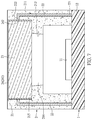
- a conventional optical module 9 includes a circuit board 91 , a chip 92 , a bracket 93 , and an optical component 94 .
- the chip 92 is disposed on the circuit board 91 .
- the bracket 93 is disposed on the circuit board 91 and surrounds the chip 92 .
- the optical component 94 is disposed on the bracket 93 .
- the chip 92 can be selected from a light-emitting chip or a light-sensing chip. When the light-emitting chip is adopted as the chip 92 , the optical component 94 is selected from a lens that has concentration, homogenization, or filtering effect according to particular implementations.
- the light-sensing chip When the light-sensing chip is adopted as the chip 92 , the light collection effect or the light guiding path needs to be considered so that a prism, a condenser lens or the like can be selected as the optical component 94 .
- the kind of the optical component 94 selected seriously influences the performance of the optical module 9 .
- the conventional optical module 9 has been used in various fields, such as lighting module of a portable electronic device, light source of an indicator light, or light sensing module for a fingerprint identifier.
- the optical module 9 is inevitably shaken or collided with, causing the optical component 94 to gradually loosen or even slip out of the bracket 93 .
- the conventional optical module 9 does not have any design for detecting whether the optical component 94 has detached or not, hence necessitating improvement in the relevant art.
- the present disclosure provides a bracket, an optical assembly, and an optical module.
- the present disclosure provides a bracket adapted to be mounted on a circuit board and support an optical component, including at least two conductive layers separated from each other; wherein the at least two conductive layers are electrically connected to the circuit board.
- the conductive layers are configured on one of the outer surface, the inner surface, and the interior of the bracket.
- the bracket further includes at least two grooves, and each of the conductive layers is respectively disposed in each of the grooves.
- the present disclosure provides an optical assembly, including a bracket and an optical component.
- the bracket includes at least two conductive layers separated from each other.
- the optical component is disposed on the bracket, and the optical component includes at least one light-transmissive conductive layer which is electrically connected to the conductive layers.
- the optical component further includes an optical component body.
- the at least one light-transmissive conductive layer is disposed on one of the upper surface and the lower surface of the optical component body, and the at least one light-transmissive conductive layer includes two conductive ends disposed on two sides of the optical component body, respectively.
- the conductive layers are configured on one of the outer surface, the inner surface, and the interior of the bracket. Each of the conductive layers includes a connecting end extending to the inner surface of the bracket, and being electrically connected to the correspondingly conductive end.
- the at least one light-transmissive conductive layer is electrically disconnected from the conductive layers when the optical component is detached from the bracket.
- the bracket further includes at least two grooves, and each of the conductive layers is respectively disposed in each of the grooves.
- the optical component further includes an optical component body on which the at least one light-transmissive conductive layer is disposed, the shape of the optical component body is rectangular, and the at least one light-transmissive conductive layer extends from one corner of the optical component body to another opposite corner thereof.
- the at least one light-transmissive conductive layer is S-shaped or strip-shaped.
- the present disclosure provides an optical module, including an electronic assembly and an optical assembly.
- the electronic assembly includes a circuit board and a chip component.
- the optical assembly is disposed on the electronic assembly, and includes a bracket and an optical component.
- the bracket surrounds the chip component and includes at least two conductive layers separated from each other.
- the conductive layers are electrically connected to the electronic assembly.
- the optical assembly is disposed on the bracket and includes at least one light-transmissive conductive layer which is electrically connected to the conductive layers.
- the optical component further includes an optical component body, and the at least one light-transmissive conductive layer is disposed on one of the upper surface and the lower surface of the optical component body.
- the at least one light-transmissive conductive layer includes two conductive ends disposed on two sides of the optical component body, respectively.
- the conductive layers are configured on one of the outer surface, the inner surface, and the interior of the bracket.
- Each of the conductive layers includes a connecting end extending to the inner surface of the bracket, and being electrically connected to the correspondingly conductive end.
- the at least one light-transmissive conductive layer is electrically disconnected from the conductive layers when the optical component is detached from the bracket.
- the bracket further includes at least two grooves, and each of the conductive layers is respectively disposed in each of the grooves.
- the optical component further includes an optical component body on which the at least one light-transmissive conductive layer is disposed.
- the shape of the optical component body is rectangular, and the at least one light-transmissive conductive layer extends from one corner of the optical component body to another opposite corner thereof.
- the at least one light-transmissive conductive layer is S-shaped or strip-shaped.
- the width of the conductive layer is larger than the width of the light-transmissive conductive layer.
- the circuit of the electronic assembly can detect whether the optical component is detached from the bracket through the conductive layers of the bracket, and can perform corresponding protection measures.
- FIG. 1 is a cross-sectional view illustrating a conventional optical module
- FIG. 2 is a perspective view illustrating a first embodiment of the present disclosure
- FIG. 3 is a cross-sectional view taken along a line of FIG. 2 , illustrating the first embodiment
- FIG. 4 is a cross-sectional view illustrating another configuration of the first embodiment
- FIG. 5 is a top view illustrating an optical component of the first embodiment
- FIG. 6 is a top view illustrating another configuration of the optical component of the first embodiment
- FIG. 7 is a cross-sectional view illustrating a second embodiment of the present disclosure.
- FIG. 8 is a cross-sectional view illustrating a third embodiment of the present disclosure.
- FIG. 9 is a cross-sectional view illustrating another variation of the third embodiment of the present disclosure.
- FIG. 10 is a cross-sectional view illustrating a fourth embodiment of the present disclosure.
- Numbering terms such as “first”, “second” or “third” can be used to describe various components, signals or the like, which are for distinguishing one component/signal from another one only, and are not intended to, nor should be construed to impose any substantive limitations on the components, signals or the like.
- a first embodiment of the present disclosure provides an optical module, including an electronic assembly 1 and an optical assembly 2 .
- the electronic assembly 1 includes a chip component 11 and a circuit board 12 .
- the chip component 11 is disposed on the circuit board 12 and is driven by a driving circuit (not shown) in the circuit board 12 .
- the chip component 11 is selected from a light-emitting chip or an optical sensor chip, but is not limited thereto.
- the light-emitting chip can be exemplified as a light-emitting diode (LED), a resonant-cavity light-emitting diode (RCLED), or a vertical-cavity surface-emitting laser chip (VCSEL), but is not limited thereto.
- the optical sensor chip can be a visible light sensing chip or a non-visible light sensing chip, and can be exemplified but not limited as a CCD chip or a CMOS chip.
- the chip being applied can be selected according to particular implementations and is not limited by the present disclosure.
- the electronic assembly 1 can be installed with a detecting circuit (not shown).
- the detecting circuit can be integrated in the chip component 11 , be disposed inside the circuit board 12 , or be the driving circuit itself which drives chip component 11 .
- the configuration of the detecting circuit can be adjusted according to particular implementations, and is not restricted hereto.
- the optical assembly 2 is disposed on the electronic assembly 1 , and includes a bracket 21 and an optical component 23 .
- the bracket 21 includes a surrounding wall 211 , a flange 212 , and two grooves 213 .
- the shape of the surrounding wall 211 is substantially a cubic cylinder that surrounds the circuit board 12 , and surroundingly defines a channel 214 .
- the shape of the surrounding wall 211 can be adjusted according to particular implementations and is not limited to a cubic cylinder, and can also be a cylinder, a polygonal cylinder, or the like.
- the flange 212 is in the channel 214 and disposed on the surrounding wall 211 , and defines an accommodating region 215 at the top of the channel 214 .
- the grooves 213 are recessed from the surface of the surrounding wall 211 , and are disposed at different sides of the surrounding wall 211 , respectively. Each groove 213 extends upward from the outside bottom of the surrounding wall 211 , passing the top of the surrounding wall 211 , and extending inward and downward to the flange 212 .
- the bracket 21 further includes two separated conductive layers 22 .
- a bottom end 221 of each conductive layer 22 is aligned with the bottom of the bracket 21 and is electrically connected to the circuit board 12 .
- Each conductive layer 22 includes a connecting end 222 for touching the optical component 23 .
- the conductive layers 22 are disposed on one of the outer surface, the inner surface, and interior of the bracket 21 . The position of the conductive layers 22 depends on particular implementations, and is not limited thereto. When the conductive layers 22 are configured on the outer surface or the inner surface of the bracket 21 , the conductive layers 22 can be formed on the bracket 21 by electroless plating or can be directly adhered to the metal sheets, but is not limited thereto.
- the connecting end 222 may extend to the top of the surrounding wall 211 , and point toward and contact with the optical component 23 ; otherwise, the connecting end 222 may extend to the inner surface of the surrounding wall 211 and be in contact with the optical component 23 .
- the connecting end 222 is exemplified as extending to the inner surface of the surrounding wall 211 .
- the conductive layers 22 can be formed, according to particular implementations, inside the groove 213 or outside the groove 213 .
- the arrangement of each conductive layer 22 may be, according to particular implementations, the same or different.
- the conductive layers 22 are exemplified as being disposed inside the grooves 213 , respectively.
- the optical component 23 is disposed inside the accommodating region 215 of the bracket 21 , and includes an optical component body and a light-transmissive conductive layer 24 .
- the shape of the optical component body complements that of the accommodating region 215 so that the shape of the optical component body is rectangular in the first embodiment.
- the optical component body has a lower surface facing the chip component 11 and an upper surface facing outside.
- the optical component body is selected from, but not limited to, a lens, a prism, or a filter.
- the lens may be exemplified as a planar lens, a condensing lens and an astigmatic lens, but is not limited thereto.
- the prism may be exemplified as a dispersion prism, a reflecting prism, and a polarizing prism, but is not limited thereto.
- the filter may be exemplified as a circular polarizer (CPL), a neutral density filter (ND filter), and a UV filter, but is not limited thereto.
- the material of the optical component body is transparent plastic or glass.
- the transparent plastic can be selected from polymethylmethacrylate (PMMA), polycarbonate (PC), polyetherimide (PEI), cyclo olefin copolymer (COC), or their mixture.
- PMMA polymethylmethacrylate
- PC polycarbonate
- PEI polyetherimide
- COC cyclo olefin copolymer
- a planar lens made of glass is taken as an example for the first embodiment.
- the light-transmissive conductive layer 24 extends from one corner of the optical component body to another opposite corner thereof.
- the light-transmissive conductive layer 24 includes a main segment 241 and two conductive ends 242 .
- the main segment 241 is disposed on the upper surface or the lower surface of the optical component body. In the first embodiment, the main segment 241 is exemplified as being disposed on the upper surface.
- the main segment 241 can be in the shape of S (shown as FIG. 5 ) or be strip-shaped (shown as FIG. 6 ). In the first embodiment, an S shape is adopted as an example, but is not limited thereto.
- the conductive ends 242 are electrically connected to the conductive layers 22 , respectively.
- the conductive ends 242 can be disposed on the same surface as the main segment 241 (shown as FIG. 3 ), or on the lateral side of the optical component body.
- the configuration of the conductive ends 242 is not limited by the present disclosure, as long as the conductive ends 242 can be electrically connected to the connecting end 222 of the conductive layer 22 .
- the conductive ends 242 are exemplified as being disposed on the upper surface of the optical component body.
- the width of the light-transmissive conductive layer 24 can be longer, shorter, or equal to the width of the conductive layer 24 , and is not limited by the present disclosure. In the first embodiment, the width of the light-transmissive conductive layer 24 is exemplified as being shorter than the width of the conductive layer.
- the light-transmissive conductive layer 24 is made of a material with light transmission and conductivity, and the material is selected from, but not limited to, metal, indium tin oxide doped tin (In 2 O 3 : Sn, ITO), tin dioxide doped fluorine (SnO 2 : F, FTO), tin dioxide doped yttrium (SnO 2 : Sb, ATO), or zinc oxide doped aluminum (ZnO: Al, AZO).
- the thickness must be less than 10 nm, and it can be exemplified as gold, silver, platinum, copper, aluminum, chromium, palladium or rhodium, but is not limited thereto.
- ITO is taken as an example.
- the conductive ends 242 of the light-transmissive conductive layer 24 are connected to the connecting ends 222 of the conductive layers 22 , respectively, that is, the conductive ends 242 are electrically connected to the detecting circuit through the conductive layers 22 to form a protection circuit.
- the detecting circuit By detecting the resistance or current of the protection circuit through the detecting circuit, it can be determined that whether the conductive layers 22 are electrically connected to the light-transmissive conductive layer 24 . Therefore, when the optical component 23 is loosened and detached from the bracket 21 , the light-transmissive conductive layer 24 would also be detached from the conductive layer 22 , and the protection circuit would be opened.
- the detecting circuit detects the open state of the protection circuit, and then shuts down the driving circuit to stop the operation of the chip component 11 , so that the chip component 11 can be prevented from being damaged.
- the driving circuit of the chip component 11 can also be shut down by connecting the protection circuit and the drive circuit in series to stop the operation of the chip component 11 when the light-transmissive conductive layer 24 is detached from the conductive layer 22 .
- the circuit of the electronic assembly 1 can detect whether the optical component 23 is detached from the bracket 21 through the conductive layers 22 disposed on the bracket 21 , and can perform corresponding protection measures.
- the circuit of the electronic assembly 1 can detect whether the optical component 23 is detached through detecting whether the light-transmissive conductive layer 24 is electrically conducted to the conductive layers 22 , and can perform corresponding protection measures.
- the worn condition of the optical component 23 can be detected. Any object scraping against the upper surface of the optical component body, would scrape the light-transmissive conductive layer 24 at the same time; therefore, the light-transmissive conductive layer 24 may be scraped off when the optical component 23 suffers from excessive scraping, which causes the protection circuit to be opened and in turn stops the operation of the chip component 11 .
- An S shape is adopted as the shape of the light-transmissive conductive layer 24 , to ensure full coverage of the light-transmissive conductive layer 24 on the optical component body, such as corners, sides, center, and so on. Therefore, this configuration can further ensure that any object scraping the optical element body would also scrape the light-transmitting conductive layer 24 at the same time, thereby improving the ability of detecting the worn condition of the optical component 23 .
- the conductive layers 22 can be prevented from being damaged by scraping, which would lead to a stop in the operation of the chip component 11 .
- the conductive layers 22 can be ensured that the protection circuit being opened is caused by the optical component 23 detaching from the bracket 21 , or the light-transmissive conductive layer 24 being damaged.
- the conductive ends 242 of the light-transmissive conductive layer 24 extending to the lateral side of the optical component body can increase the contact area with the conductive layer 22 , and can ensure an effective electrical connection therebetween. Therefore, only when the optical component 23 is almost or completely detached from the bracket 21 will the light-transmissive conductive layer 24 not be in contact with the conductive layers 23 , so that the protection circuit becomes opened. Accordingly, this configuration can prevent misjudgment of the detecting circuit due to any mismatch from shaking between the conductive layers 22 and the light-transmissive conductive layer 24 .
- the conductive layer 22 and the light-transmissive conductive layer 24 can be electrically connected with each other even when production error is factored in.
- a second embodiment of the present disclosure is approximately the same as the first embodiment, but a main difference between the present embodiment and the first embodiment is that the conductive ends 242 of the light-transmissive conductive layer 24 extend to the lateral side of the optical components body, and the conductive layer 22 is disposed in the interior of the bracket 21 . Since the conductive layer 22 is disposed in the interior of the bracket 21 , the bracket 21 does not include the grooves 213 (shown at FIG. 2 ) in the second embodiment.
- the method by which the conductive layers 22 are disposed inside the bracket 21 can be adjusted based on the material and the process of the bracket 21 .
- the method may be: putting the conductive layers 22 in a mold for making the bracket 21 , and then injecting the thermoplastic material into the mold and wrapping the conductive layers 22 ; finally, curing the thermoplastic material to form the bracket 21 .
- the method may be: inserting the conductive layers 22 into a blank, and then sintering them together so that the conductive layers 22 are buried in the bracket 21 .
- the method can be adjusted according to any conventional method and is not limited thereto.
- the structure of the conductive layers 22 buried in the bracket 21 can prevent the conductive layers 22 from damage by scraping, and can further ensure that the protection circuit being opened is due to the optical component 23 detaching from the bracket 21 or the light-transmissive conductive layer 24 being damaged, and is not due to the conductive layers 22 themselves being damaged.
- the second embodiment has the same advantages as the first embodiment, and by burying the conductive layers 22 in the bracket 21 , this structure can further ensure the accuracy of detecting whether the optical component 23 is detached from the bracket 21 or suffering from excessive scraping.
- a third embodiment of the present disclosure is approximately the same as the first embodiment, but a main difference between the present embodiment and the first embodiment is that the light-transmissive conductive layer 24 is disposed on the lower surface of the optical component body. Since the connecting ends 222 of the conductive layers 22 are extended near the lower surface of the optical component body, the connecting ends 222 can be electronically connected to the light-transmissive conductive layer 24 .
- the conductive layers 22 are disposed on the inner surface of the bracket 21 .
- the bottom ends 221 are electrically connected to the circuit board, and the connecting ends 222 extend to the upper side of the flange 212 of the bracket 21 .
- the light-transmissive conductive layer 24 and the conductive layers 22 can be bonded and electrically connected with each other.
- the third embodiment has the same advantages as the first embodiment except that the worn condition of the optical component 23 cannot be detected.
- Manufacturers can choose any configuration mentioned above according to particular implementations.
- the optical module need not have the function of detecting the worn condition of the optical component 23
- the present embodiment may be applied. Accordingly, the third embodiment provides another technical solution that allows the manufacturer to make adjustments according to particular implementations.
- a fourth embodiment of the present disclosure is approximately the same as the third embodiment, but a main difference between the present embodiment and the third embodiment is that the conductive ends 242 of the light-transmissive conductive layer 24 extend to the lateral side of the optical component body, and the conductive layers 22 are disposed in the interior of the bracket 21 .
- the configuration of the conductive layers 22 is the same as the second embodiment, and hence is not described herein.
- the fourth embodiment has the same advantages as the third embodiment.
- this structure can further ensure the accuracy of detecting whether the optical component 23 is detached from the bracket 21 or whether the optical component 23 is suffering from excessive scraping.
- the conductive layers 22 disposed on the bracket 21 can allow the circuit of circuit board 12 to detect whether the optical component 23 is detached from the bracket 21 , and perform corresponding protection measures.
Landscapes
- Physics & Mathematics (AREA)
- General Physics & Mathematics (AREA)
- Optics & Photonics (AREA)
- Light Receiving Elements (AREA)
- Optical Couplings Of Light Guides (AREA)
- Semiconductor Lasers (AREA)
- Led Devices (AREA)
- Mounting And Adjusting Of Optical Elements (AREA)
- Led Device Packages (AREA)
Abstract
Description
Claims (4)
Applications Claiming Priority (3)
| Application Number | Priority Date | Filing Date | Title |
|---|---|---|---|
| TW107120028 | 2018-06-11 | ||
| TW107120028A | 2018-06-11 | ||
| TW107120028A TWI697019B (en) | 2018-06-11 | 2018-06-11 | Holder, optical component and optical module |
Publications (2)
| Publication Number | Publication Date |
|---|---|
| US20190378936A1 US20190378936A1 (en) | 2019-12-12 |
| US10763375B2 true US10763375B2 (en) | 2020-09-01 |
Family
ID=68764226
Family Applications (1)
| Application Number | Title | Priority Date | Filing Date |
|---|---|---|---|
| US16/124,238 Active US10763375B2 (en) | 2018-06-11 | 2018-09-07 | Optical assembly and optical module |
Country Status (5)
| Country | Link |
|---|---|
| US (1) | US10763375B2 (en) |
| JP (1) | JP6660438B2 (en) |
| KR (1) | KR102087288B1 (en) |
| CN (1) | CN110581111A (en) |
| TW (1) | TWI697019B (en) |
Families Citing this family (3)
| Publication number | Priority date | Publication date | Assignee | Title |
|---|---|---|---|---|
| DE102020124008A1 (en) | 2020-09-15 | 2022-03-17 | OSRAM Opto Semiconductors Gesellschaft mit beschränkter Haftung | PROCESS FOR MAKING A PACKAGE AND OPTOELECTRONIC DEVICE |
| CN113677088A (en) * | 2021-09-29 | 2021-11-19 | 深圳市海谱纳米光学科技有限公司 | An optical filter assembly for mounting on a circuit board |
| JP2023054547A (en) * | 2021-10-04 | 2023-04-14 | ソニーセミコンダクタソリューションズ株式会社 | Light source device, distance measurement device, and equipment |
Citations (14)
| Publication number | Priority date | Publication date | Assignee | Title |
|---|---|---|---|---|
| JP2000331577A (en) | 1999-05-18 | 2000-11-30 | Omron Corp | Photoelectric sensor and method of manufacturing the same |
| CN102375292A (en) | 2010-08-20 | 2012-03-14 | 林小军 | Device for controlling tilting or rotation center of optical system and actuator |
| US20140043496A1 (en) * | 2012-08-10 | 2014-02-13 | Eddie Azuma | Camera module with compact sponge absorbing design |
| JP2014165450A (en) | 2013-02-27 | 2014-09-08 | Stanley Electric Co Ltd | Semiconductor light-emitting device |
| JP2014190823A (en) | 2013-03-27 | 2014-10-06 | Sanyo Electric Co Ltd | Information acquisition device and object detector |
| JP2015060159A (en) | 2013-09-20 | 2015-03-30 | カシオ計算機株式会社 | Fluorescent light emitting device and projector |
| JP2015109331A (en) | 2013-12-04 | 2015-06-11 | シャープ株式会社 | Nitride semiconductor light emitting device |
| CN104755978A (en) | 2012-08-10 | 2015-07-01 | 南昌欧菲光电技术有限公司 | Auto-focus camera module with flexible printed circuit extension |
| JP2016009693A (en) | 2014-06-23 | 2016-01-18 | スタンレー電気株式会社 | Light emitting device and lighting device |
| US20160020239A1 (en) * | 2014-07-16 | 2016-01-21 | Semiconductor Manufacturing International (Shanghai) Corporation | 3d integrated cis |
| WO2017092694A1 (en) | 2015-12-01 | 2017-06-08 | 宁波舜宇光电信息有限公司 | Photographing module and electric bracket thereof |
| US20180003927A1 (en) * | 2016-06-29 | 2018-01-04 | Heptagon Micro Optics Pte. Ltd. | Optical and optoelectronic assemblies including micro-spacers, and methods of manufacturing the same |
| US20180160545A1 (en) * | 2016-12-05 | 2018-06-07 | Samsung Electronics Co., Ltd. | Mounting structure for module in electronic device |
| US20190204528A1 (en) * | 2016-07-14 | 2019-07-04 | Mitsubishi Electric Corporation | Illumination device |
Family Cites Families (11)
| Publication number | Priority date | Publication date | Assignee | Title |
|---|---|---|---|---|
| CN101162698A (en) * | 2006-10-12 | 2008-04-16 | 矽品精密工业股份有限公司 | Sensing type package and manufacturing method thereof |
| TWI359481B (en) * | 2007-12-28 | 2012-03-01 | Siliconware Precision Industries Co Ltd | Sensor semiconductor package and method thereof |
| GB0801509D0 (en) * | 2008-01-28 | 2008-03-05 | Photonstar Led Ltd | Light emitting system with optically transparent thermally conductive element |
| TWI390324B (en) * | 2009-03-06 | 2013-03-21 | Primax Electronics Ltd | Camera module and method for manufacturing and cleaning same |
| JP5566061B2 (en) * | 2009-07-31 | 2014-08-06 | オリンパス株式会社 | Optical displacement detector |
| US10296774B2 (en) * | 2014-09-18 | 2019-05-21 | Huawei Technologies Co., Ltd. | Fingerprint recognition apparatus |
| JP2016099193A (en) * | 2014-11-20 | 2016-05-30 | 東洋ゴム工業株式会社 | Method for manufacturing deformation detection sensor for sealed secondary battery |
| US20180247962A1 (en) * | 2015-08-28 | 2018-08-30 | China Wafer Level Csp Co., Ltd. | Image sensor package structure and packaging method thereof |
| CN105472217B (en) * | 2015-12-01 | 2021-01-26 | 宁波舜宇光电信息有限公司 | Electrical support with EMI shielding conductive layer, camera module and assembly method thereof |
| CN206807600U (en) * | 2017-05-24 | 2017-12-26 | 深圳市依诺普电子科技有限公司 | A kind of radially connected medical camera module |
| TWM570523U (en) * | 2018-06-11 | 2018-11-21 | 海華科技股份有限公司 | Holder, optical component and optical module |
-
2018
- 2018-06-11 TW TW107120028A patent/TWI697019B/en active
- 2018-06-19 CN CN201810628352.XA patent/CN110581111A/en active Pending
- 2018-09-07 US US16/124,238 patent/US10763375B2/en active Active
- 2018-09-11 KR KR1020180108154A patent/KR102087288B1/en active Active
- 2018-09-19 JP JP2018174709A patent/JP6660438B2/en active Active
Patent Citations (15)
| Publication number | Priority date | Publication date | Assignee | Title |
|---|---|---|---|---|
| JP2000331577A (en) | 1999-05-18 | 2000-11-30 | Omron Corp | Photoelectric sensor and method of manufacturing the same |
| CN102375292A (en) | 2010-08-20 | 2012-03-14 | 林小军 | Device for controlling tilting or rotation center of optical system and actuator |
| CN104755978A (en) | 2012-08-10 | 2015-07-01 | 南昌欧菲光电技术有限公司 | Auto-focus camera module with flexible printed circuit extension |
| US20140043496A1 (en) * | 2012-08-10 | 2014-02-13 | Eddie Azuma | Camera module with compact sponge absorbing design |
| JP2014165450A (en) | 2013-02-27 | 2014-09-08 | Stanley Electric Co Ltd | Semiconductor light-emitting device |
| JP2014190823A (en) | 2013-03-27 | 2014-10-06 | Sanyo Electric Co Ltd | Information acquisition device and object detector |
| JP2015060159A (en) | 2013-09-20 | 2015-03-30 | カシオ計算機株式会社 | Fluorescent light emitting device and projector |
| JP2015109331A (en) | 2013-12-04 | 2015-06-11 | シャープ株式会社 | Nitride semiconductor light emitting device |
| JP2016009693A (en) | 2014-06-23 | 2016-01-18 | スタンレー電気株式会社 | Light emitting device and lighting device |
| US20160020239A1 (en) * | 2014-07-16 | 2016-01-21 | Semiconductor Manufacturing International (Shanghai) Corporation | 3d integrated cis |
| WO2017092694A1 (en) | 2015-12-01 | 2017-06-08 | 宁波舜宇光电信息有限公司 | Photographing module and electric bracket thereof |
| US20180352127A1 (en) * | 2015-12-01 | 2018-12-06 | Ningbo Sunny Opotech Co., Ltd. | Photographing module and electric bracket thereof |
| US20180003927A1 (en) * | 2016-06-29 | 2018-01-04 | Heptagon Micro Optics Pte. Ltd. | Optical and optoelectronic assemblies including micro-spacers, and methods of manufacturing the same |
| US20190204528A1 (en) * | 2016-07-14 | 2019-07-04 | Mitsubishi Electric Corporation | Illumination device |
| US20180160545A1 (en) * | 2016-12-05 | 2018-06-07 | Samsung Electronics Co., Ltd. | Mounting structure for module in electronic device |
Also Published As
| Publication number | Publication date |
|---|---|
| JP2019216227A (en) | 2019-12-19 |
| TWI697019B (en) | 2020-06-21 |
| JP6660438B2 (en) | 2020-03-11 |
| KR102087288B1 (en) | 2020-03-11 |
| CN110581111A (en) | 2019-12-17 |
| TW202001951A (en) | 2020-01-01 |
| US20190378936A1 (en) | 2019-12-12 |
Similar Documents
| Publication | Publication Date | Title |
|---|---|---|
| US10692905B2 (en) | Optical component, optical assembly and optical module | |
| US8624585B2 (en) | Proximity sensor | |
| US10763375B2 (en) | Optical assembly and optical module | |
| US10738985B2 (en) | Housing for light source | |
| US20110298739A1 (en) | Touch-sensitive device and touch-sensitive display device | |
| TWI691671B (en) | Flip chip light emitting module | |
| CN209895058U (en) | Optical element | |
| US10004140B2 (en) | Three-dimensional circuit substrate and sensor module using three-dimensional circuit substrate | |
| US20200251458A1 (en) | Light source device | |
| US11588074B2 (en) | Light source device | |
| TWM570523U (en) | Holder, optical component and optical module | |
| US10884552B2 (en) | Touch panel with sensor elements | |
| JP2007013050A (en) | Reflective photosensor | |
| KR101030459B1 (en) | Capacitive Touch Sensor Module | |
| US11217572B2 (en) | Light source device | |
| US20140118632A1 (en) | Projected capacitive touch panel | |
| CN221650952U (en) | Optical fingerprint sensing device | |
| US11868541B2 (en) | Optical detection device and optical navigation apparatus | |
| CN111211204A (en) | Flip chip light emitting module | |
| KR20250150715A (en) | Electronic device | |
| KR20160005594A (en) | Touch window |
Legal Events
| Date | Code | Title | Description |
|---|---|---|---|
| AS | Assignment |
Owner name: AZUREWAVE TECHNOLOGIES, INC., TAIWAN Free format text: ASSIGNMENT OF ASSIGNORS INTEREST;ASSIGNORS:LIN, KUNG-AN;YANG, CHUNG-CHE;LU, MING-CHUN;REEL/FRAME:046809/0657 Effective date: 20180830 |
|
| FEPP | Fee payment procedure |
Free format text: ENTITY STATUS SET TO UNDISCOUNTED (ORIGINAL EVENT CODE: BIG.); ENTITY STATUS OF PATENT OWNER: SMALL ENTITY |
|
| FEPP | Fee payment procedure |
Free format text: ENTITY STATUS SET TO SMALL (ORIGINAL EVENT CODE: SMAL); ENTITY STATUS OF PATENT OWNER: SMALL ENTITY |
|
| STPP | Information on status: patent application and granting procedure in general |
Free format text: NON FINAL ACTION MAILED |
|
| STPP | Information on status: patent application and granting procedure in general |
Free format text: RESPONSE TO NON-FINAL OFFICE ACTION ENTERED AND FORWARDED TO EXAMINER |
|
| STPP | Information on status: patent application and granting procedure in general |
Free format text: NON FINAL ACTION MAILED |
|
| STPP | Information on status: patent application and granting procedure in general |
Free format text: NOTICE OF ALLOWANCE MAILED -- APPLICATION RECEIVED IN OFFICE OF PUBLICATIONS |
|
| STCF | Information on status: patent grant |
Free format text: PATENTED CASE |
|
| MAFP | Maintenance fee payment |
Free format text: PAYMENT OF MAINTENANCE FEE, 4TH YR, SMALL ENTITY (ORIGINAL EVENT CODE: M2551); ENTITY STATUS OF PATENT OWNER: SMALL ENTITY Year of fee payment: 4 |