US10714558B2 - Display panel and display device - Google Patents
Display panel and display device Download PDFInfo
- Publication number
- US10714558B2 US10714558B2 US15/299,639 US201615299639A US10714558B2 US 10714558 B2 US10714558 B2 US 10714558B2 US 201615299639 A US201615299639 A US 201615299639A US 10714558 B2 US10714558 B2 US 10714558B2
- Authority
- US
- United States
- Prior art keywords
- area
- display panel
- display
- display device
- sub
- Prior art date
- Legal status (The legal status is an assumption and is not a legal conclusion. Google has not performed a legal analysis and makes no representation as to the accuracy of the status listed.)
- Active, expires
Links
- 239000000758 substrate Substances 0.000 claims description 44
- 239000010410 layer Substances 0.000 claims description 18
- 239000012044 organic layer Substances 0.000 claims description 16
- 239000011521 glass Substances 0.000 claims description 4
- 238000005452 bending Methods 0.000 claims 2
- 238000011161 development Methods 0.000 description 4
- 230000004044 response Effects 0.000 description 3
- 238000005070 sampling Methods 0.000 description 3
- MSFGZHUJTJBYFA-UHFFFAOYSA-M sodium dichloroisocyanurate Chemical compound [Na+].ClN1C(=O)[N-]C(=O)N(Cl)C1=O MSFGZHUJTJBYFA-UHFFFAOYSA-M 0.000 description 3
- 239000003990 capacitor Substances 0.000 description 2
- 238000013461 design Methods 0.000 description 2
- 238000005516 engineering process Methods 0.000 description 2
- 239000004973 liquid crystal related substance Substances 0.000 description 2
- 238000000034 method Methods 0.000 description 2
- 238000012986 modification Methods 0.000 description 2
- 230000004048 modification Effects 0.000 description 2
- 238000000059 patterning Methods 0.000 description 2
- 230000008569 process Effects 0.000 description 2
- 230000002457 bidirectional effect Effects 0.000 description 1
- 239000002184 metal Substances 0.000 description 1
- 239000004033 plastic Substances 0.000 description 1
- 229920001721 polyimide Polymers 0.000 description 1
- 238000012545 processing Methods 0.000 description 1
- 239000000126 substance Substances 0.000 description 1
Images


Classifications
-
- H—ELECTRICITY
- H10—SEMICONDUCTOR DEVICES; ELECTRIC SOLID-STATE DEVICES NOT OTHERWISE PROVIDED FOR
- H10K—ORGANIC ELECTRIC SOLID-STATE DEVICES
- H10K59/00—Integrated devices, or assemblies of multiple devices, comprising at least one organic light-emitting element covered by group H10K50/00
- H10K59/10—OLED displays
- H10K59/12—Active-matrix OLED [AMOLED] displays
- H10K59/128—Active-matrix OLED [AMOLED] displays comprising two independent displays, e.g. for emitting information from two major sides of the display
-
- G—PHYSICS
- G09—EDUCATION; CRYPTOGRAPHY; DISPLAY; ADVERTISING; SEALS
- G09G—ARRANGEMENTS OR CIRCUITS FOR CONTROL OF INDICATING DEVICES USING STATIC MEANS TO PRESENT VARIABLE INFORMATION
- G09G3/00—Control arrangements or circuits, of interest only in connection with visual indicators other than cathode-ray tubes
- G09G3/20—Control arrangements or circuits, of interest only in connection with visual indicators other than cathode-ray tubes for presentation of an assembly of a number of characters, e.g. a page, by composing the assembly by combination of individual elements arranged in a matrix no fixed position being assigned to or needed to be assigned to the individual characters or partial characters
-
- H01L27/3267—
-
- G—PHYSICS
- G09—EDUCATION; CRYPTOGRAPHY; DISPLAY; ADVERTISING; SEALS
- G09G—ARRANGEMENTS OR CIRCUITS FOR CONTROL OF INDICATING DEVICES USING STATIC MEANS TO PRESENT VARIABLE INFORMATION
- G09G3/00—Control arrangements or circuits, of interest only in connection with visual indicators other than cathode-ray tubes
- G09G3/03—Control arrangements or circuits, of interest only in connection with visual indicators other than cathode-ray tubes specially adapted for displays having non-planar surfaces, e.g. curved displays
- G09G3/035—Control arrangements or circuits, of interest only in connection with visual indicators other than cathode-ray tubes specially adapted for displays having non-planar surfaces, e.g. curved displays for flexible display surfaces
-
- G—PHYSICS
- G09—EDUCATION; CRYPTOGRAPHY; DISPLAY; ADVERTISING; SEALS
- G09G—ARRANGEMENTS OR CIRCUITS FOR CONTROL OF INDICATING DEVICES USING STATIC MEANS TO PRESENT VARIABLE INFORMATION
- G09G3/00—Control arrangements or circuits, of interest only in connection with visual indicators other than cathode-ray tubes
- G09G3/20—Control arrangements or circuits, of interest only in connection with visual indicators other than cathode-ray tubes for presentation of an assembly of a number of characters, e.g. a page, by composing the assembly by combination of individual elements arranged in a matrix no fixed position being assigned to or needed to be assigned to the individual characters or partial characters
- G09G3/22—Control arrangements or circuits, of interest only in connection with visual indicators other than cathode-ray tubes for presentation of an assembly of a number of characters, e.g. a page, by composing the assembly by combination of individual elements arranged in a matrix no fixed position being assigned to or needed to be assigned to the individual characters or partial characters using controlled light sources
- G09G3/28—Control arrangements or circuits, of interest only in connection with visual indicators other than cathode-ray tubes for presentation of an assembly of a number of characters, e.g. a page, by composing the assembly by combination of individual elements arranged in a matrix no fixed position being assigned to or needed to be assigned to the individual characters or partial characters using controlled light sources using luminous gas-discharge panels, e.g. plasma panels
-
- G—PHYSICS
- G09—EDUCATION; CRYPTOGRAPHY; DISPLAY; ADVERTISING; SEALS
- G09G—ARRANGEMENTS OR CIRCUITS FOR CONTROL OF INDICATING DEVICES USING STATIC MEANS TO PRESENT VARIABLE INFORMATION
- G09G3/00—Control arrangements or circuits, of interest only in connection with visual indicators other than cathode-ray tubes
- G09G3/20—Control arrangements or circuits, of interest only in connection with visual indicators other than cathode-ray tubes for presentation of an assembly of a number of characters, e.g. a page, by composing the assembly by combination of individual elements arranged in a matrix no fixed position being assigned to or needed to be assigned to the individual characters or partial characters
- G09G3/22—Control arrangements or circuits, of interest only in connection with visual indicators other than cathode-ray tubes for presentation of an assembly of a number of characters, e.g. a page, by composing the assembly by combination of individual elements arranged in a matrix no fixed position being assigned to or needed to be assigned to the individual characters or partial characters using controlled light sources
- G09G3/30—Control arrangements or circuits, of interest only in connection with visual indicators other than cathode-ray tubes for presentation of an assembly of a number of characters, e.g. a page, by composing the assembly by combination of individual elements arranged in a matrix no fixed position being assigned to or needed to be assigned to the individual characters or partial characters using controlled light sources using electroluminescent panels
- G09G3/32—Control arrangements or circuits, of interest only in connection with visual indicators other than cathode-ray tubes for presentation of an assembly of a number of characters, e.g. a page, by composing the assembly by combination of individual elements arranged in a matrix no fixed position being assigned to or needed to be assigned to the individual characters or partial characters using controlled light sources using electroluminescent panels semiconductive, e.g. using light-emitting diodes [LED]
- G09G3/3208—Control arrangements or circuits, of interest only in connection with visual indicators other than cathode-ray tubes for presentation of an assembly of a number of characters, e.g. a page, by composing the assembly by combination of individual elements arranged in a matrix no fixed position being assigned to or needed to be assigned to the individual characters or partial characters using controlled light sources using electroluminescent panels semiconductive, e.g. using light-emitting diodes [LED] organic, e.g. using organic light-emitting diodes [OLED]
- G09G3/3225—Control arrangements or circuits, of interest only in connection with visual indicators other than cathode-ray tubes for presentation of an assembly of a number of characters, e.g. a page, by composing the assembly by combination of individual elements arranged in a matrix no fixed position being assigned to or needed to be assigned to the individual characters or partial characters using controlled light sources using electroluminescent panels semiconductive, e.g. using light-emitting diodes [LED] organic, e.g. using organic light-emitting diodes [OLED] using an active matrix
- G09G3/3233—Control arrangements or circuits, of interest only in connection with visual indicators other than cathode-ray tubes for presentation of an assembly of a number of characters, e.g. a page, by composing the assembly by combination of individual elements arranged in a matrix no fixed position being assigned to or needed to be assigned to the individual characters or partial characters using controlled light sources using electroluminescent panels semiconductive, e.g. using light-emitting diodes [LED] organic, e.g. using organic light-emitting diodes [OLED] using an active matrix with pixel circuitry controlling the current through the light-emitting element
- G09G3/3241—Control arrangements or circuits, of interest only in connection with visual indicators other than cathode-ray tubes for presentation of an assembly of a number of characters, e.g. a page, by composing the assembly by combination of individual elements arranged in a matrix no fixed position being assigned to or needed to be assigned to the individual characters or partial characters using controlled light sources using electroluminescent panels semiconductive, e.g. using light-emitting diodes [LED] organic, e.g. using organic light-emitting diodes [OLED] using an active matrix with pixel circuitry controlling the current through the light-emitting element the current through the light-emitting element being set using a data current provided by the data driver, e.g. by using a two-transistor current mirror
- G09G3/325—Control arrangements or circuits, of interest only in connection with visual indicators other than cathode-ray tubes for presentation of an assembly of a number of characters, e.g. a page, by composing the assembly by combination of individual elements arranged in a matrix no fixed position being assigned to or needed to be assigned to the individual characters or partial characters using controlled light sources using electroluminescent panels semiconductive, e.g. using light-emitting diodes [LED] organic, e.g. using organic light-emitting diodes [OLED] using an active matrix with pixel circuitry controlling the current through the light-emitting element the current through the light-emitting element being set using a data current provided by the data driver, e.g. by using a two-transistor current mirror the data current flowing through the driving transistor during a setting phase, e.g. by using a switch for connecting the driving transistor to the data driver
-
- G—PHYSICS
- G09—EDUCATION; CRYPTOGRAPHY; DISPLAY; ADVERTISING; SEALS
- G09G—ARRANGEMENTS OR CIRCUITS FOR CONTROL OF INDICATING DEVICES USING STATIC MEANS TO PRESENT VARIABLE INFORMATION
- G09G3/00—Control arrangements or circuits, of interest only in connection with visual indicators other than cathode-ray tubes
- G09G3/20—Control arrangements or circuits, of interest only in connection with visual indicators other than cathode-ray tubes for presentation of an assembly of a number of characters, e.g. a page, by composing the assembly by combination of individual elements arranged in a matrix no fixed position being assigned to or needed to be assigned to the individual characters or partial characters
- G09G3/22—Control arrangements or circuits, of interest only in connection with visual indicators other than cathode-ray tubes for presentation of an assembly of a number of characters, e.g. a page, by composing the assembly by combination of individual elements arranged in a matrix no fixed position being assigned to or needed to be assigned to the individual characters or partial characters using controlled light sources
- G09G3/30—Control arrangements or circuits, of interest only in connection with visual indicators other than cathode-ray tubes for presentation of an assembly of a number of characters, e.g. a page, by composing the assembly by combination of individual elements arranged in a matrix no fixed position being assigned to or needed to be assigned to the individual characters or partial characters using controlled light sources using electroluminescent panels
- G09G3/32—Control arrangements or circuits, of interest only in connection with visual indicators other than cathode-ray tubes for presentation of an assembly of a number of characters, e.g. a page, by composing the assembly by combination of individual elements arranged in a matrix no fixed position being assigned to or needed to be assigned to the individual characters or partial characters using controlled light sources using electroluminescent panels semiconductive, e.g. using light-emitting diodes [LED]
- G09G3/3208—Control arrangements or circuits, of interest only in connection with visual indicators other than cathode-ray tubes for presentation of an assembly of a number of characters, e.g. a page, by composing the assembly by combination of individual elements arranged in a matrix no fixed position being assigned to or needed to be assigned to the individual characters or partial characters using controlled light sources using electroluminescent panels semiconductive, e.g. using light-emitting diodes [LED] organic, e.g. using organic light-emitting diodes [OLED]
- G09G3/3266—Details of drivers for scan electrodes
-
- G—PHYSICS
- G09—EDUCATION; CRYPTOGRAPHY; DISPLAY; ADVERTISING; SEALS
- G09G—ARRANGEMENTS OR CIRCUITS FOR CONTROL OF INDICATING DEVICES USING STATIC MEANS TO PRESENT VARIABLE INFORMATION
- G09G3/00—Control arrangements or circuits, of interest only in connection with visual indicators other than cathode-ray tubes
- G09G3/20—Control arrangements or circuits, of interest only in connection with visual indicators other than cathode-ray tubes for presentation of an assembly of a number of characters, e.g. a page, by composing the assembly by combination of individual elements arranged in a matrix no fixed position being assigned to or needed to be assigned to the individual characters or partial characters
- G09G3/22—Control arrangements or circuits, of interest only in connection with visual indicators other than cathode-ray tubes for presentation of an assembly of a number of characters, e.g. a page, by composing the assembly by combination of individual elements arranged in a matrix no fixed position being assigned to or needed to be assigned to the individual characters or partial characters using controlled light sources
- G09G3/30—Control arrangements or circuits, of interest only in connection with visual indicators other than cathode-ray tubes for presentation of an assembly of a number of characters, e.g. a page, by composing the assembly by combination of individual elements arranged in a matrix no fixed position being assigned to or needed to be assigned to the individual characters or partial characters using controlled light sources using electroluminescent panels
- G09G3/32—Control arrangements or circuits, of interest only in connection with visual indicators other than cathode-ray tubes for presentation of an assembly of a number of characters, e.g. a page, by composing the assembly by combination of individual elements arranged in a matrix no fixed position being assigned to or needed to be assigned to the individual characters or partial characters using controlled light sources using electroluminescent panels semiconductive, e.g. using light-emitting diodes [LED]
- G09G3/3208—Control arrangements or circuits, of interest only in connection with visual indicators other than cathode-ray tubes for presentation of an assembly of a number of characters, e.g. a page, by composing the assembly by combination of individual elements arranged in a matrix no fixed position being assigned to or needed to be assigned to the individual characters or partial characters using controlled light sources using electroluminescent panels semiconductive, e.g. using light-emitting diodes [LED] organic, e.g. using organic light-emitting diodes [OLED]
- G09G3/3275—Details of drivers for data electrodes
- G09G3/3291—Details of drivers for data electrodes in which the data driver supplies a variable data voltage for setting the current through, or the voltage across, the light-emitting elements
-
- G—PHYSICS
- G09—EDUCATION; CRYPTOGRAPHY; DISPLAY; ADVERTISING; SEALS
- G09G—ARRANGEMENTS OR CIRCUITS FOR CONTROL OF INDICATING DEVICES USING STATIC MEANS TO PRESENT VARIABLE INFORMATION
- G09G3/00—Control arrangements or circuits, of interest only in connection with visual indicators other than cathode-ray tubes
- G09G3/20—Control arrangements or circuits, of interest only in connection with visual indicators other than cathode-ray tubes for presentation of an assembly of a number of characters, e.g. a page, by composing the assembly by combination of individual elements arranged in a matrix no fixed position being assigned to or needed to be assigned to the individual characters or partial characters
- G09G3/34—Control arrangements or circuits, of interest only in connection with visual indicators other than cathode-ray tubes for presentation of an assembly of a number of characters, e.g. a page, by composing the assembly by combination of individual elements arranged in a matrix no fixed position being assigned to or needed to be assigned to the individual characters or partial characters by control of light from an independent source
- G09G3/36—Control arrangements or circuits, of interest only in connection with visual indicators other than cathode-ray tubes for presentation of an assembly of a number of characters, e.g. a page, by composing the assembly by combination of individual elements arranged in a matrix no fixed position being assigned to or needed to be assigned to the individual characters or partial characters by control of light from an independent source using liquid crystals
- G09G3/3611—Control of matrices with row and column drivers
- G09G3/3648—Control of matrices with row and column drivers using an active matrix
-
- H01L27/3276—
-
- H01L51/5012—
-
- H01L51/5206—
-
- H01L51/5221—
-
- H01L51/5271—
-
- H—ELECTRICITY
- H10—SEMICONDUCTOR DEVICES; ELECTRIC SOLID-STATE DEVICES NOT OTHERWISE PROVIDED FOR
- H10K—ORGANIC ELECTRIC SOLID-STATE DEVICES
- H10K50/00—Organic light-emitting devices
- H10K50/10—OLEDs or polymer light-emitting diodes [PLED]
- H10K50/11—OLEDs or polymer light-emitting diodes [PLED] characterised by the electroluminescent [EL] layers
-
- H—ELECTRICITY
- H10—SEMICONDUCTOR DEVICES; ELECTRIC SOLID-STATE DEVICES NOT OTHERWISE PROVIDED FOR
- H10K—ORGANIC ELECTRIC SOLID-STATE DEVICES
- H10K50/00—Organic light-emitting devices
- H10K50/80—Constructional details
- H10K50/805—Electrodes
- H10K50/81—Anodes
-
- H—ELECTRICITY
- H10—SEMICONDUCTOR DEVICES; ELECTRIC SOLID-STATE DEVICES NOT OTHERWISE PROVIDED FOR
- H10K—ORGANIC ELECTRIC SOLID-STATE DEVICES
- H10K50/00—Organic light-emitting devices
- H10K50/80—Constructional details
- H10K50/805—Electrodes
- H10K50/82—Cathodes
-
- H—ELECTRICITY
- H10—SEMICONDUCTOR DEVICES; ELECTRIC SOLID-STATE DEVICES NOT OTHERWISE PROVIDED FOR
- H10K—ORGANIC ELECTRIC SOLID-STATE DEVICES
- H10K50/00—Organic light-emitting devices
- H10K50/80—Constructional details
- H10K50/85—Arrangements for extracting light from the devices
- H10K50/856—Arrangements for extracting light from the devices comprising reflective means
-
- H—ELECTRICITY
- H10—SEMICONDUCTOR DEVICES; ELECTRIC SOLID-STATE DEVICES NOT OTHERWISE PROVIDED FOR
- H10K—ORGANIC ELECTRIC SOLID-STATE DEVICES
- H10K59/00—Integrated devices, or assemblies of multiple devices, comprising at least one organic light-emitting element covered by group H10K50/00
- H10K59/10—OLED displays
- H10K59/12—Active-matrix OLED [AMOLED] displays
- H10K59/131—Interconnections, e.g. wiring lines or terminals
-
- H—ELECTRICITY
- H10—SEMICONDUCTOR DEVICES; ELECTRIC SOLID-STATE DEVICES NOT OTHERWISE PROVIDED FOR
- H10K—ORGANIC ELECTRIC SOLID-STATE DEVICES
- H10K59/00—Integrated devices, or assemblies of multiple devices, comprising at least one organic light-emitting element covered by group H10K50/00
- H10K59/80—Constructional details
- H10K59/875—Arrangements for extracting light from the devices
- H10K59/878—Arrangements for extracting light from the devices comprising reflective means
-
- G—PHYSICS
- G09—EDUCATION; CRYPTOGRAPHY; DISPLAY; ADVERTISING; SEALS
- G09G—ARRANGEMENTS OR CIRCUITS FOR CONTROL OF INDICATING DEVICES USING STATIC MEANS TO PRESENT VARIABLE INFORMATION
- G09G2300/00—Aspects of the constitution of display devices
- G09G2300/08—Active matrix structure, i.e. with use of active elements, inclusive of non-linear two terminal elements, in the pixels together with light emitting or modulating elements
- G09G2300/0809—Several active elements per pixel in active matrix panels
-
- G—PHYSICS
- G09—EDUCATION; CRYPTOGRAPHY; DISPLAY; ADVERTISING; SEALS
- G09G—ARRANGEMENTS OR CIRCUITS FOR CONTROL OF INDICATING DEVICES USING STATIC MEANS TO PRESENT VARIABLE INFORMATION
- G09G2310/00—Command of the display device
- G09G2310/02—Addressing, scanning or driving the display screen or processing steps related thereto
- G09G2310/0264—Details of driving circuits
- G09G2310/027—Details of drivers for data electrodes, the drivers handling digital grey scale data, e.g. use of D/A converters
-
- G—PHYSICS
- G09—EDUCATION; CRYPTOGRAPHY; DISPLAY; ADVERTISING; SEALS
- G09G—ARRANGEMENTS OR CIRCUITS FOR CONTROL OF INDICATING DEVICES USING STATIC MEANS TO PRESENT VARIABLE INFORMATION
- G09G2310/00—Command of the display device
- G09G2310/02—Addressing, scanning or driving the display screen or processing steps related thereto
- G09G2310/0264—Details of driving circuits
- G09G2310/0286—Details of a shift registers arranged for use in a driving circuit
-
- G—PHYSICS
- G09—EDUCATION; CRYPTOGRAPHY; DISPLAY; ADVERTISING; SEALS
- G09G—ARRANGEMENTS OR CIRCUITS FOR CONTROL OF INDICATING DEVICES USING STATIC MEANS TO PRESENT VARIABLE INFORMATION
- G09G2310/00—Command of the display device
- G09G2310/02—Addressing, scanning or driving the display screen or processing steps related thereto
- G09G2310/0264—Details of driving circuits
- G09G2310/0291—Details of output amplifiers or buffers arranged for use in a driving circuit
-
- G—PHYSICS
- G09—EDUCATION; CRYPTOGRAPHY; DISPLAY; ADVERTISING; SEALS
- G09G—ARRANGEMENTS OR CIRCUITS FOR CONTROL OF INDICATING DEVICES USING STATIC MEANS TO PRESENT VARIABLE INFORMATION
- G09G2380/00—Specific applications
- G09G2380/02—Flexible displays
-
- H01L2251/5315—
-
- H01L2251/5323—
-
- H01L2251/533—
-
- H01L2251/5338—
-
- H01L51/0097—
-
- H—ELECTRICITY
- H10—SEMICONDUCTOR DEVICES; ELECTRIC SOLID-STATE DEVICES NOT OTHERWISE PROVIDED FOR
- H10K—ORGANIC ELECTRIC SOLID-STATE DEVICES
- H10K2102/00—Constructional details relating to the organic devices covered by this subclass
- H10K2102/301—Details of OLEDs
- H10K2102/302—Details of OLEDs of OLED structures
- H10K2102/3023—Direction of light emission
- H10K2102/3026—Top emission
-
- H—ELECTRICITY
- H10—SEMICONDUCTOR DEVICES; ELECTRIC SOLID-STATE DEVICES NOT OTHERWISE PROVIDED FOR
- H10K—ORGANIC ELECTRIC SOLID-STATE DEVICES
- H10K2102/00—Constructional details relating to the organic devices covered by this subclass
- H10K2102/301—Details of OLEDs
- H10K2102/302—Details of OLEDs of OLED structures
- H10K2102/3023—Direction of light emission
- H10K2102/3031—Two-side emission, e.g. transparent OLEDs [TOLED]
-
- H—ELECTRICITY
- H10—SEMICONDUCTOR DEVICES; ELECTRIC SOLID-STATE DEVICES NOT OTHERWISE PROVIDED FOR
- H10K—ORGANIC ELECTRIC SOLID-STATE DEVICES
- H10K2102/00—Constructional details relating to the organic devices covered by this subclass
- H10K2102/301—Details of OLEDs
- H10K2102/302—Details of OLEDs of OLED structures
- H10K2102/3023—Direction of light emission
- H10K2102/3035—Edge emission
-
- H—ELECTRICITY
- H10—SEMICONDUCTOR DEVICES; ELECTRIC SOLID-STATE DEVICES NOT OTHERWISE PROVIDED FOR
- H10K—ORGANIC ELECTRIC SOLID-STATE DEVICES
- H10K2102/00—Constructional details relating to the organic devices covered by this subclass
- H10K2102/301—Details of OLEDs
- H10K2102/311—Flexible OLED
-
- H—ELECTRICITY
- H10—SEMICONDUCTOR DEVICES; ELECTRIC SOLID-STATE DEVICES NOT OTHERWISE PROVIDED FOR
- H10K—ORGANIC ELECTRIC SOLID-STATE DEVICES
- H10K59/00—Integrated devices, or assemblies of multiple devices, comprising at least one organic light-emitting element covered by group H10K50/00
- H10K59/80—Constructional details
- H10K59/805—Electrodes
- H10K59/8051—Anodes
-
- H—ELECTRICITY
- H10—SEMICONDUCTOR DEVICES; ELECTRIC SOLID-STATE DEVICES NOT OTHERWISE PROVIDED FOR
- H10K—ORGANIC ELECTRIC SOLID-STATE DEVICES
- H10K59/00—Integrated devices, or assemblies of multiple devices, comprising at least one organic light-emitting element covered by group H10K50/00
- H10K59/80—Constructional details
- H10K59/805—Electrodes
- H10K59/8052—Cathodes
-
- H—ELECTRICITY
- H10—SEMICONDUCTOR DEVICES; ELECTRIC SOLID-STATE DEVICES NOT OTHERWISE PROVIDED FOR
- H10K—ORGANIC ELECTRIC SOLID-STATE DEVICES
- H10K77/00—Constructional details of devices covered by this subclass and not covered by groups H10K10/80, H10K30/80, H10K50/80 or H10K59/80
- H10K77/10—Substrates, e.g. flexible substrates
- H10K77/111—Flexible substrates
Definitions
- the present disclosure relates to a display panel and a display device.
- LCD liquid crystal display
- PDP plasma display panels
- organic light-emitting display devices are used.
- products for use in double-sided display devices, opposite surfaces thereof being able to emit light, as well as flexible display devices, are also being developed.
- the present invention is directed to a display panel and a display device that substantially obviate one or more of the problems due to limitations and disadvantages of the related art.
- An object of the present disclosure is to provide a novel display panel having a double-sided light-emitting structure able to satisfy rapidly-changing user demands and a display device including the same.
- Another object of the present disclosure is to provide a display panel divided into two areas having different light-emitting directions and a display device including the same.
- Another object of the present disclosure is to provide a display panel having both a top emission structure and a bottom emission structure on a single substrate and a display device including the same.
- Another object of the present disclosure is to provide a foldable display panel able to display various types of additional information or images in a folded state and a foldable display device including the same.
- a display device comprises a display panel having a plurality of data lines and a plurality of gate lines thereon, the display panel including at least one first area and at least one second area having different light-emitting directions; a data driver circuit configured to drive the plurality of data lines; and a gate driver circuit configured to drive the plurality of gate lines.
- a display panel comprises a substrate; a first electrode on the substrate; an organic layer on the first electrode; and a second electrode on the organic layer, wherein the display panel includes at least one first area and at least one second area having different light-emitting directions, and wherein the display panel further includes: a bottom reflective layer between the substrate and the first electrode in the first area, and a top reflective layer on the second electrode in the second area.
- a display device comprises a body foldable into a plurality of parts; and a driver chip within the body, wherein a front screen is provided on at least one first part among the plurality of parts, and a rear screen is provided on at least one second part among the plurality of parts other than the first part, and wherein, when the display device is folded, the rear screen provided on the at least one second part is exposed externally to display additional information including at least one of characters, symbols, and images.
- FIG. 1 is a configuration view illustrating a display device according to example embodiments of the present invention
- FIG. 2 to FIG. 9 illustrate examples of display panels according to example embodiments of the present invention.
- FIG. 10 and FIG. 11 are cross-sectional views of the display panels according to example embodiments of the present invention.
- FIG. 12 to FIG. 17 illustrate examples of folding lines of the display panels according to example embodiments of the present invention.
- FIG. 18 to FIG. 22 illustrate the folded states of the display panels according to example embodiments of the present invention.
- FIG. 23 illustrates gate lines on the display panel according to example embodiments of the present invention.
- FIG. 24 illustrates data lines on the display panel according to example embodiments of the present invention.
- FIG. 25 illustrates a gate driving performed on the first area and the second area of the display panel according to example embodiments of the present invention
- FIG. 26 illustrates a data driving performed on the first area and the second area of the display panel according to example embodiments of the present invention
- FIG. 27 is a cross-sectional view of the display panel according to example embodiments of the present invention.
- FIG. 28 to FIG. 30 illustrate a mobile device as a product application of a display device in which the display panel according to example embodiments of the present invention is used.
- FIG. 31 illustrates a public display device as another product application of a display device using the display panel according to example embodiments of the present invention.
- FIG. 1 is a configuration view illustrating a display device 100 according to example embodiments of the present invention.
- the display device 100 may include a display panel 110 , a data driver circuit 120 , a gate driver circuit 130 , and a controller 140 .
- the display panel 110 has a plurality of data lines, a plurality of gate lines, and a plurality of subpixels disposed thereon.
- the data driver circuit 120 drives the plurality of data lines, while the gate driver circuit 130 drives the plurality of gate lines.
- the controller 140 controls the data driver circuit 120 and the gate driver circuit 130 .
- the controller 140 is able to supply a variety of control signals to the data driver circuit 120 and the gate driver circuit 130 to control the data driver circuit 120 and the gate driver circuit 130 .
- the controller 140 starts scanning based on timing realized by each frame, converts image data input from an external source into a data signal format readable by the data driver circuit 120 , outputs the converted image data, and at a suitable point in time, controls data processing in response to the scanning.
- the controller 140 may be a timing controller used in display technology or may be a control device including the timing controller and configured to perform other control functions.
- the data driver circuit 120 drives the plurality of data lines by converting image data received from the controller 140 into analog data voltages and supplying the analog data voltages to the plurality of data lines.
- the data driver circuit 120 will also be referred to as a “source driver.”
- the gate driver circuit 130 sequentially drives the plurality of gate lines by sequentially supplying scanning signals to the plurality of gate lines.
- the gate driver circuit 130 will also be referred to as a “scanning driver.”
- the gate driver circuit 130 sequentially supplies scanning signals, respectively having an on or off voltage, to the plurality of gate lines under the control of the controller 140 .
- the data driver circuit 120 in FIG. 1 is illustrated as being positioned on one side of (e.g., above or below) the display panel 110 , the data driver circuit 120 may be positioned on either or both sides of (e.g., above and below) the display panel 110 depending on the driving system, the design of the panel, and so on.
- the data driver circuit 120 may include the controller 140 .
- the gate driver circuit 130 in FIG. 1 is illustrated as being positioned on one side (e.g., to the left or to the right) of the display panel 110 , the gate driver circuit 130 may be positioned on either or both sides (e.g., to the left and to the right) of the display panel 110 .
- the gate driver circuit 130 and the data driver circuit 120 may be integrated to form an integrated driver chip.
- the controller 140 receives a variety of timing signals, including a vertical synchronization signal Vsync, a horizontal synchronization signal Hsync, an input data enable (DE) signal, and a clock signal, as well as input image data, from an external source (e.g., an external host system).
- a vertical synchronization signal Vsync a horizontal synchronization signal Hsync
- an input data enable (DE) signal e.g., an external host system
- the controller 140 not only outputs image data input from an external source by converting the image data into a data signal format readable by the source driver circuit 120 , but also receives the variety of received timing signals (including the vertical synchronization signal Vsync, the horizontal synchronization signal Hsync, the input DE signal, and the clock signal), generates a variety of control signals, and outputs the variety of control signals to the source driver circuit 120 and the scanning driver circuit 130 to control the source driver circuit 120 and the scanning driver circuit 130 .
- the controller 140 outputs a variety of gate control signals (GCSs), including a gate start pulse (GSP), a gate shift clock (GSC) signal, and a gate output enable (GOE) signal, to control the scanning driver 130 .
- GCSs gate control signals
- GSP gate start pulse
- GSC gate shift clock
- GOE gate output enable
- the GSP controls the operation start timing of one or more gate driver ICs (GDICs) of the scanning driver circuit 130 .
- the GSC signal is a clock signal commonly input to the GDICs to control the shift timing of scanning signals (gate pulses).
- the GOE signal designates the timing information of one or more GDICs.
- the controller 140 outputs a variety of data control signals (DCSs), including a source start pulse (SSP), a source sampling clock (SSC) signal, and a source output enable (SOE) signal, to control the source driver circuit 120 .
- DCSs data control signals
- SSP controls the data sampling start timing of one or more SDICs of the source driver circuit 120 .
- SSC signal is a clock signal controlling the data sampling timing of each of the SDICs.
- the SOE signal controls the output timing of the source driver circuit 120 .
- the source driver circuit 120 may include one or more source driver ICs (SDICs).
- Each of the SDICs may be connected to the bonding pads of the display panel 110 by tape automated bonding (TAB) or chip on glass (COG) bonding, may be directly disposed on the display panel 110 , or in some cases, may be integrated with the display panel 110 .
- each of the SDICs may be mounted on a film connected to the display panel 100 by a chip on film (COF) process.
- Each of the SDICs may include a shift register, a latch circuit, a digital-to-analog converter (DAC), an output buffer, and so on.
- each of the SDICs may further include an analog-to-digital converter (ADC).
- ADC analog-to-digital converter
- the gate driver circuit 130 may include one or more gate driver integrated circuits (GDICs).
- GDICs gate driver integrated circuits
- Each of the GDICs may be connected to the bonding pads of the display panel 110 by tape automated bonding (TAB) or chip on glass (COG) bonding, may be implemented as a gate in panel (GIP)-type IC directly disposed on the display panel 110 , or in some cases, may be integrated with the display panel 110 .
- GDICs gate in panel
- each of the GDICs may be mounted on a film connected to the display panel 100 by a chip on film (COF) process.
- COF chip on film
- Each of the GDICs may include a shift register, a level shifter, and so on.
- the display panel 110 may include at least one source printed circuit board (S-PCB) required to connect at least one SDIC in the circuit and a control printed circuit board (C-PCB) on which control components and a variety electronic devices are mounted. At least one SDIC may be mounted on the at least one S-PCB, or a film on which at least one SDIC is mounted may be connected to the at least one S-PCB.
- S-PCB source printed circuit board
- C-PCB control printed circuit board
- the controller 140 controlling the operations of the data driver circuit 120 and the gate driver circuit 130 may be mounted on the C-PCB.
- a power controller supplying a variety of voltages or currents or controlling a variety of voltages or currents to be supplied to the display panel 110 , the data driver circuit 120 , the gate driver circuit 130 , and the like may be disposed on the C-PCB
- the at least one S-PCB and the C-PCB may be connected in the circuit via at least one connector.
- the connector may be implemented as a flexible flat cable (FFC), a flexible printed circuit (FPC), or so on.
- the at least one S-PCB and the C-PCB may be integrated as a single PCB.
- the display panel 110 may be one of various types of devices, such as a liquid crystal display (LCD) device, an organic light-emitting display device, and a plasma display panel (PDP). Each of the subpixels disposed on the display panel 110 may include a circuit device, such as a transistor.
- LCD liquid crystal display
- PDP plasma display panel
- each of the subpixels may include an organic light-emitting diode (OLED), a transistor T 1 driving the OLED, a switching transistor T 2 delivering a data voltage Vdata to a gate node of the driving transistor T 1 , a storage capacitor C 1 connecting a gate node and a source node (or a drain node) of the driving transistor T 1 , and so on.
- OLED organic light-emitting diode
- T 1 driving the OLED a switching transistor T 2 delivering a data voltage Vdata to a gate node of the driving transistor T 1
- a storage capacitor C 1 connecting a gate node and a source node (or a drain node) of the driving transistor T 1 , and so on.
- the OLED includes a first electrode, an organic layer, and a second electrode.
- the first electrode may be an anode or a cathode
- the second electrode may be a cathode or an anode.
- a base voltage EVSS is connected to the second electrode.
- the driving transistor T 1 is controlled by the data voltage Vdata applied to the gate node.
- a driving voltage EVDD is applied to the drain node (or the source node) of the driving transistor T 1 .
- the source node (or the drain node) of the driving transistor T 1 is connected to the first electrode (the anode or the cathode) of the OLED.
- the switching transistor T 2 is controlled by a scanning signal SCAN applied to the gate node through the gate line GL.
- the switching transistor T 2 switches the data voltage Vdata applied to the drain node or the source node through the data line DL to output through the source node or the drain node so that the data voltage Vdata is delivered to the gate node of the driving transistor T 1 .
- the storage capacitor C 1 maintains a predetermined level of voltage for a single frame.
- the types and number of circuit elements constituting each of the subpixels SP may be variously added to or altered depending on the functions to be provided and the design.
- the display panel 110 may be divided into at least one first area A 1 and at least one second area A 2 .
- the at least one first area A 1 and the at least one second area A 2 do not overlap each other and have different light-emitting directions.
- the first area A 1 may have a top emission structure, while the second area A 2 may have a bottom emission structure.
- the first area A 1 may have a bottom emission structure, while the second area A 2 may have a top emission structure.
- first area A 1 having a top or bottom emission structure may be a front display area
- second area A 2 having a bottom or top emission structure may be a rear display area
- first area A 1 may be a rear display area
- second area A 2 may be a front display area
- the display panel 110 differs from a typical double-sided display panel in that one area A 1 or A 2 has top emission structure while the other area A 2 or A 1 has a bottom emission structure.
- bidirectional light emissions a realized by stacking two display panels configured to emit light in the same direction such that the display panels are oriented in the opposite directions, by patterning light-emitting devices configured to emit light in the same direction in the top and bottom portions of a single substrate, or by patterning a light-emitting device configured to emit in the same direction on one surface of a single substrate and then folding the substrate.
- the display panel 110 according to the present embodiments is configured such that top emissions and bottom emissions are realized separately in the two divided areas A 1 and A 2 .
- the use of the display panel 110 according to the present embodiments can provide new and varied product applications that cannot be created by typical double-sided display panels.
- Both the first area A 1 and the second area A 2 may be image display areas.
- one of the first area A 1 and the second area A 2 may be an image display area and the other of the first area A 1 and the second area A 2 may be an additional information display area.
- new and varied of display devices can be produced using both the first and second areas A 1 and A 2 as image display areas or one of the first and second areas A 1 and A 2 as an additional information display area.
- the display panel 110 designed to be divided by a variety of patterns. That is, the display panel 110 is designed such that various numbers of the first area A 1 and the second area A 2 are formed at a variety of positions.
- FIG. 2 to FIG. 9 illustrate examples of the display panel 110 according to example embodiments of the present invention.
- the size of the second area A 2 may be smaller than the size of the first area A 1 . Because the second area A 2 is set to be smaller than the first area A 1 as described above, the display panel 110 may be designed such that the first area A 1 is used as a main display area and the second area A 2 is used as a sub-display area.
- the additional information may include at least one type of information selected from among information regarding the statuses of a variety of devices (e.g., information regarding a battery, communications information, and update information), content information, channel information, news information, weather information, information regarding telecommunications conversation, message information, and so on.
- information regarding the statuses of a variety of devices e.g., information regarding a battery, communications information, and update information
- content information e.g., information regarding a battery, communications information, and update information
- content information e.g., channel information, news information, weather information, information regarding telecommunications conversation, message information, and so on.
- the size of each of the first areas A 1 may correspond to the size of each of the second areas A 2 . That is, a single first area A 1 and a single second area A 2 may have the same size. Because the single first area A 1 and the single second area A 2 have the same size as described above, both the first area A 1 and the second area A 2 can be used as a main display area.
- the length L 2 of the second area A 2 in the first direction may correspond to the length L 1 of the first area A 1 in the first direction.
- the display panel 110 in which the first area A 1 and the second area A 2 have the same length may be used in the development of a variety of new products.
- the length L 2 of the second area A 2 in the first direction may be shorter than the length L 1 of the first area A 1 in the first direction.
- the display panel 110 in which the length of the second area A 2 is shorter than the length of the first area A 1 may be used in the development of a variety of new products.
- the length L 2 of each of the second areas A 2 in the first direction may be designed to be half the length L 1 of the first area A 1 in the first direction.
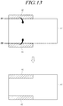
- FIG. 10 and FIG. 11 are cross-sectional views of the display panels 110 according to example embodiments of the present embodiments.
- FIG. 10 and FIG. 11 illustrate the cross-section taken along line X-X′ in FIG. 5 and the cross-section taken along line Y-Y′ in FIG. 7 when the display panels 110 are organic light-emitting display panels.
- a multilayer structure is provided in each of the first area A 1 and the second area A 2 .
- the multilayer structure includes a substrate 500 , a first electrode 510 disposed on the substrate 500 , an organic layer 520 disposed on the first electrode 510 , and a second electrode 530 disposed on the organic layer 520 .
- the first area A 1 and the second area A 2 have different light-emitting directions.
- a bottom reflective layer LR may be further disposed between the substrate 500 and the first electrode 510 in one of the first area A 1 and the second area A 2
- a top reflective layer UR may be further disposed on the second electrode 530 in the other of the first area A 1 and the second area A 2
- the first area A 1 may be a top emission area
- the second area A 2 may be a bottom emission area.
- the bottom reflective layer LR may be further disposed between the substrate 500 and the first electrode 510 in the first area A 1 , thereby realizing a top emission structure.
- the top reflective layer UR may be further disposed on the second electrode 530 in the second area A 2 , thereby realizing a bottom emission structure.
- the bottom reflective layer LR is further disposed between the substrate 500 and the first electrode 510 in one of the first area A 1 and the second area A 2
- the top reflective layer UR is further disposed on the other of the first area A 1 and the second area A 2 , whereby the first area A 1 and the second area A 2 can have different light-emitting directions.
- the substrate 500 may be a flexible glass substrate or a flexible film substrate.
- the flexible film substrate may be, for example, a plastic substrate, a polyimide film, or the like.
- a flexible display device can be produced by fabricating the display panel 110 using the above-described substrate 500 .
- the display device 100 according to the present embodiments may be a foldable device.
- FIG. 12 to FIG. 17 illustrate examples of folding lines FP of the display panels 110 according to example embodiments of the present invention.
- each of the display panels 110 can be folded along the folding points FP between the first area A 1 and the second area A 2 .
- the display panel 110 can be folded along the folding points FP at which the first area A 1 or the second area A 2 is divided into two or more sub-areas.
- the display panel 110 can be folded along the folding points FP between the two sub-areas A 1 a and A 1 b.
- a folding pattern suitable to the position and size of the divided areas A 1 and A 2 of the display panel 110 can be provided by folding the display panel 110 along the boundary between the first area A 1 and the second area A 2 or along points by which the first or second area A 1 or A 2 is divided into two or more sub-areas.
- the second area A 2 can cover all or a portion of the first area A 1 .
- the first area A 1 is entirely covered with the second area A 2 such that the first area A 1 is not externally exposed. That is, the rear surfaces of the second area A 2 act as covers to conceal the entirety of the first area A 1 .
- the second areas A 2 can act as covers to close all or portions of the first area A 1 .
- the single first area A 1 is divided into the two sub-areas A 1 a and A 1 b
- each of the two sub-areas A 2 is divided into two sub-areas A 2 a and A 2 b .
- the left sub-area A 1 a of the first area A 1 is covered with the right sub-area A 1 b of the first area A 1
- the left sub-areas A 2 a of the second areas A 2 are covered with the right sub-areas A 2 b of the second areas A 2 .
- the single first area A 1 is divided into the two sub-areas A 1 a and A 1 b .
- the right sub-area A 1 b of the first area A 1 is covered with the left sub-area A 1 a of the first area A 1 .
- At least one sub-area A 1 b or A 1 a can cover the other sub-area A 1 a or A 1 b.
- FIG. 18 to FIG. 22 illustrate the folded states of the display panels 110 according to example embodiments of the present invention.
- FIG. 18 to FIG. 20 illustrate the display panels 110 illustrated in FIG. 12 , FIG. 14 , and FIG. 15 , which are emitting light in the folded states.
- FIG. 21 and FIG. 22 illustrate the display panels 110 illustrated in FIG. 16 and FIG. 17 , which are emitting light in the folded states.
- one area A 1 or A 2 of the first area A 1 and the second area A 2 may be a display-on area (e.g., an area that is being display-driven), and the other area A 2 or A 1 of the first area A 1 and the second area A 2 may be a display-off area (e.g., an area that is not being display-driven).
- a display-on area e.g., an area that is being display-driven
- the other area A 2 or A 1 of the first area A 1 and the second area A 2 may be a display-off area (e.g., an area that is not being display-driven).
- the first area A 1 is covered with the rear surfaces of the second areas A 2 .
- the front surface of the first area A 1 e.g., the light-emitting surface
- the second areas A 2 covering the first area A 1 emit light through the rear surfaces, e.g., the light-emitting surfaces, due to the bottom emission structure thereof.
- one sub-area A 1 a or A 1 b of the first area A 1 covers the other sub-area A 1 b or A 1 a of the first area A 1 .
- the single first area A 1 is divided into the two sub-areas A 1 a and A 1 b
- each of the two second areas A 2 is divided into the two sub-areas A 2 a and A 2 b .
- the right sub-area A 1 b of the first area A 1 covers the left sub-area Ala of the first area A 1
- the right sub-areas A 2 b of the second areas A 2 cover the left sub-areas A 2 a of the second areas A 2 .
- the front surface of the first area A 1 corresponding to the emission surface does not generate light
- the right sub-areas A 2 b of the second areas A 2 covering the left sub-areas A 2 a of the second areas A 2 emit light through the rear surfaces, e.g., the light-emitting surfaces, due to the bottom emission structure thereof.
- the single first area A 1 is divided into the two sub-areas A 1 a and A 1 b .
- the left sub-area Ala of the first area A 1 covers the right sub-area A 1 b of the first area A 1 .
- the second areas A 2 having the bottom emission structure emit light through the rear surfaces, e.g., the light-emitting surfaces.
- a user can check various types of additional information from the second areas A 2 , which emit light through bottom emissions, without unfolding (e.g., opening) the folded display panel 110 .
- FIG. 23 illustrates gate lines GL 1 and GL 2 on the display panel 110 according to example embodiments of the present invention.
- the boundaries BL between the first area A 1 and the second areas A 2 are parallel to the gate lines GL 1 and GL 2 .
- the gate lines GL 1 disposed in the first area A 1 and the gate lines disposed in the second areas A 2 are parallel to the boundaries BL between the first area A 1 and the second areas A 2 .
- the display panels 110 as illustrated in FIG. 2 to FIG. 6 can be fabricated.
- first area A 1 and the second areas A 2 are disposed such that the boundaries therebetween are parallel to the gate lines GL 1 and GL 2 , it may be convenient to independently perform gate driving over the first area A 1 and the second areas A 2 . Consequently, it may be easy to independently control the display statuses of the first area A 1 and the second areas A 2 .
- gate driving can be controlled to be performed only on the first area A 1 so that only the first area A 1 is display-driven.
- gate driving can be controlled to be performed only on the second area A 2 so that only the second area A 2 is display-driven.
- FIG. 24 illustrates data lines DL 1 and DL 2 on the display panel 110 according to example embodiments of the present invention.
- the boundary BL between the first area A 1 and the second area A 2 of the display panel 110 is parallel to the data lines DL 1 and DL 2 .
- the data lines DL 1 in the first area A 1 , and the data lines DL 2 in the second area A 2 are parallel to the boundary BL between the first area A 1 and the second area A 2 .
- the display panels 110 as illustrated in FIG. 7 to FIG. 9 can be fabricated.
- the first area A 1 and the second areas A 2 are disposed such that the boundary BL therebetween is parallel to the data lines DL 1 and DL 2 . It may be convenient to independently perform data driving on the first area A 1 and the second area A 2 . It may thereby be convenient to independently control display driving on the first area and the second area A 2 .
- data driving can be controlled to be performed only on the first area A 1 so that only the first area A 1 is display-driven.
- data driving can be controlled to be performed only on the second area A 2 so that only the second area A 2 is display-driven.
- the display panel 110 is divided into at least one first area A 1 and at least one second area A 2 , wherein the divided areas A 1 and A 2 can be gate-driven independently or can be gate-driven without being distinguished from each other.
- the divided areas A 1 and A 2 in the display panel 110 can be data-driven independently or can be data-driven without being distinguished from each other.
- the gate driver circuit 130 and the data driver circuit 120 may be configured as illustrated in FIG. 25 and FIG. 26 .
- FIG. 25 illustrates gate driving performed on the first area A 1 and the second area A 2 of the display panel 110 according to example embodiments of the present invention.
- the gate driver circuit 130 of the display device 100 may include a first gate driver GD 1 driving gate lines through which subpixels disposed in the first area A 1 are controlled to generate light and a second gate driver GD 2 driving gate lines through which subpixels disposed in the second area A 2 are controlled to generate light.
- the subpixels disposed in the first area A 1 may have a top emission structure, while the subpixels disposed in the second area A 2 may have a bottom emission structure.
- the gate driver circuit 130 includes the gate drivers GD 1 and GD 2 , each of which drives the corresponding area, as described above, the first area A 1 and the second area A 2 can be independently gate-driven. Consequently, it may be convenient to control the display statuses of the first area A 1 and the second area A 2 independently.
- gate driving can be controlled to be performed so that only the first area A 1 is display-driven.
- gate driving can be controlled to be performed so that only the second area A 2 is display-driven.
- the controller 140 can control the operations of the first gate driver GD 1 and the second gate driver GD 2 based on the status of the device, such as whether or not the display panel is folded, the positions of the areas, or so on.
- FIG. 26 illustrates data driving performed on the first area A 1 and the second area A 2 of the display panel 110 according to example embodiments of the present invention.
- the data driver circuit 120 of the display device 100 includes a first data driver DD 1 driving data lines through which subpixels disposed in the first area A 1 are controlled to generate light and a second data driver DD 2 driving data lines through which subpixels disposed in the second area A 2 are controlled to generate light.
- the subpixels disposed in the first area A 1 may have a top emission structure, while the subpixels disposed in the second area A 2 may have a bottom emission structure.
- the data driver circuit 120 includes the data drivers DD 1 and DD 2 , each of which drives the corresponding area, as described above, the first area A 1 and the second area A 2 can be independently data-driven. Consequently, it may be convenient to control the display statuses of the first area A 1 and the second area A 2 independently.
- first data driver DD 1 sequentially drives only the gate lines DL 1 disposed in the first area A 1
- data driving can be controlled to be performed so that only the first area A 1 is display-driven.
- second data driver DD 2 sequentially drives only the data lines DL 2 disposed in the second area A 2
- data driving can be controlled to be performed so that only the second area A 2 is display-driven.
- the controller 140 can control the operations of the first data driver DD 1 and the second data driver DD 2 based on the status of the device such as whether or not the display panel is folded, the positions of the areas, or so on.
- the display panel 110 is divided into the at least one first area A 1 and the at least one second area A 2 .
- one area (e.g., the second area A 2 ) of the first area A 1 and the second area A 2 is an additional information display area (e.g., a sub-display area) in which additional information rather than images is displayed
- the additional information display area is not required to be a high-resolution area, unlike an image display area (e.g., a main display area).
- one area of the first area A 1 and the second area A 2 may be a lower-resolution area compared to the other area, although the resolution of one area may be equal to that of the other area.
- the gate lines and the data lines are disposed such that the number (or density) of the sub-pixels of the lower-resolution area is smaller than that of the sub-pixels of higher-resolution area.
- one area of the first area A 1 and the second area A 2 may be designed to be a lower-resolution area, such that patterns can be designed more easily.
- the first area A 1 and the second area A 2 can be gate-driven and data-driven independently.
- FIG. 27 is a cross-sectional view of the display panel 110 according to example embodiments of the present invention.
- the display panel 110 may include a substrate 500 , a top emission device TED disposed in the first area A 1 of the substrate 500 , and a bottom emission device BED disposed in the second area A 2 of the substrate 500 .
- the top emission device TED and the bottom emission device BED are positioned on the same substrate 500 .
- circuit elements such as transistors, (e.g., T 1 , T 2 , C 1 , and so on) are disposed on the substrate 500 .
- the display panel 110 may include the substrate 500 , a first electrode 510 disposed on the substrate 500 , an organic layer 520 disposed on the first electrode 510 , and a second electrode 530 disposed on the organic layer 520 .
- the first electrode 510 may be an anode of an organic light-emitting diode (OLED), while the second electrode 530 may be a cathode of the OLED.
- the first electrode 510 and the second electrode 530 may be transparent electrodes or thin-metal electrodes that are thin enough to be transparent.
- the display panel 110 is divided into at least one first area A 1 and at least one second area A 2 .
- the at least one first area A 1 and the at least one second area A 2 have different light-emitting directions
- the display panel 110 further includes a bottom reflective layer LR disposed between the substrate 500 and the first electrode 510 in the first area A 1 and a top reflective UR disposed on the second electrode 530 in the second area A 2 .
- the novel display panel 110 having a double-sided light-emitting structure can be realized by dividing the single display panel 110 into at least one first area A 1 and at least one second area A 2 and forming the at least one first area A 1 and the at least one second area A 2 formed on the same substrate 500 to have a top emission structure and a bottom emission structure. Accordingly, new and varied product applications that cannot be created by typical double-sided display panels can be provided.
- FIG. 28 to FIG. 30 illustrate a mobile device 2800 as a product application of a display device 2800 in which the display panel 110 according to example embodiments of the present invention is used.
- the mobile device 2800 using the display panel 110 includes a body 2810 foldable into a plurality of parts P 1 and P 2 and a driver chip 2820 disposed within the body 2810 .
- At least one first part P 1 of the plurality of parts P 1 and P 2 has a front screen FS, and at least one of second parts P 2 of the plurality of parts P 1 and P 2 has a rear screen RS.
- the front screen FS in the position in which the mobile device 2800 , a product application of the display device 100 , is folded, the front screen FS is folded to be completely concealed, while the rear screens RS disposed on the second parts P 2 may display additional information, including at least one of characters, symbols, and images, thereon.
- the light-emitting direction of the front screen FS differs from that of the rear screens RS.
- the front screen FS corresponds to the first area A 1 , in which the bottom emission device BED or the top emission device TED is disposed in every subpixel on the substrate 500 .
- the rear screens RS correspond to the second areas A 2 , in which the bottom emission device BED or the top emission device TED is disposed in every subpixel on the substrate 500 .
- the top emission device TED includes the bottom reflective layer LR disposed on the substrate 500 , the first electrode 510 disposed on the bottom reflective layer LR, the organic layer 520 disposed on the first electrode 520 , the second electrode 530 disposed on the organic layer 520 , and so on.
- the bottom emission device BED includes the first electrode 510 disposed on the substrate 500 , the organic layer 520 disposed on the first electrode 510 , the second electrode 530 disposed on the organic layer 520 , and the top reflective layer UR disposed on the second electrode 530 .
- the mobile device 2800 is foldable to protect the front screen FS corresponding to a main display screen. In the folded state, various types of additional information may be displayed on the rear screens RS respectively designed to have a bottom emission structure.
- FIG. 31 illustrates a public display device 3100 as another product application of a display device 3100 using the display panel 110 according to example embodiments of the present invention.
- the public display device 3100 includes the display panel 110 of FIG. 14 .
- a front screen FS corresponding to the top-emitting first area 1 can display an image or information of an object 1 positioned on the rear side of a rear screen RS corresponding to the second area A 2 .
- the rear screen RS corresponding to the bottom-emitting second area A 2 can display an image or information of an object 2 positioned on the rear side of the front screen FS corresponding to the first area A 1 .
- the novel display panel 110 having a double-sided light-emitting structure able to satisfy rapidly-changing user demands and the display device 100 including the same.
- the display panel 110 divided into two areas having different light-emitting directions and the display device 100 including the same.
- the display panel 110 having both a top emission structure and a bottom emission structure on a single substrate and the display device 100 including the same.
- the foldable display panel 110 able to display various types of additional information or images in a folded state and the foldable display device 100 including the same.
Abstract
Description
Claims (21)
Applications Claiming Priority (2)
| Application Number | Priority Date | Filing Date | Title |
|---|---|---|---|
| KR1020150146907A KR102403205B1 (en) | 2015-10-21 | 2015-10-21 | Display panel and display device |
| KR10-2015-0146907 | 2015-10-21 |
Publications (2)
| Publication Number | Publication Date |
|---|---|
| US20170117342A1 US20170117342A1 (en) | 2017-04-27 |
| US10714558B2 true US10714558B2 (en) | 2020-07-14 |
Family
ID=58558995
Family Applications (1)
| Application Number | Title | Priority Date | Filing Date |
|---|---|---|---|
| US15/299,639 Active 2036-11-25 US10714558B2 (en) | 2015-10-21 | 2016-10-21 | Display panel and display device |
Country Status (3)
| Country | Link |
|---|---|
| US (1) | US10714558B2 (en) |
| KR (1) | KR102403205B1 (en) |
| CN (1) | CN106935171B (en) |
Cited By (2)
| Publication number | Priority date | Publication date | Assignee | Title |
|---|---|---|---|---|
| US20200044003A1 (en) * | 2017-03-24 | 2020-02-06 | Samsung Electronics Co., Ltd. | Flexible display and electronic device including same |
| US20220209175A1 (en) * | 2020-03-31 | 2022-06-30 | Boe Technology Group Co., Ltd. | Oled display panel, method of forming display panel and display device |
Families Citing this family (12)
| Publication number | Priority date | Publication date | Assignee | Title |
|---|---|---|---|---|
| CN104464540B (en) * | 2014-12-25 | 2016-04-20 | 京东方科技集团股份有限公司 | Display panel, display panel assembly and manufacture method thereof, display device |
| US11296173B2 (en) | 2017-12-08 | 2022-04-05 | Hewlett-Packard Development Company, L.P. | Dual-sided displays |
| KR20200142394A (en) * | 2019-06-12 | 2020-12-22 | 엘지디스플레이 주식회사 | Foldable display and driving method thereof |
| KR20210056468A (en) * | 2019-11-08 | 2021-05-20 | 삼성디스플레이 주식회사 | Sensing unit and display device including the same |
| CN110827759B (en) * | 2019-11-19 | 2021-03-05 | 上海天马有机发光显示技术有限公司 | Display panel and display device |
| CN110850627A (en) * | 2019-11-29 | 2020-02-28 | 厦门天马微电子有限公司 | Display panel and display device |
| CN110942724A (en) * | 2019-12-19 | 2020-03-31 | 武汉华星光电半导体显示技术有限公司 | Folding display panel and display device |
| CN111028760B (en) * | 2019-12-26 | 2022-08-23 | 武汉华星光电半导体显示技术有限公司 | Display panel and driving method thereof |
| US11385734B2 (en) * | 2020-06-23 | 2022-07-12 | Microsoft Technology Licensing, Llc | Multi-panel display device |
| CN111968579A (en) * | 2020-09-07 | 2020-11-20 | 京东方科技集团股份有限公司 | Display panel and wearable device |
| KR20230013688A (en) * | 2021-07-16 | 2023-01-27 | 삼성디스플레이 주식회사 | Display device and manufacturing method for the same |
| CN114170919A (en) * | 2021-12-13 | 2022-03-11 | Tcl华星光电技术有限公司 | Double-sided display panel and double-sided display splicing screen |
Citations (19)
| Publication number | Priority date | Publication date | Assignee | Title |
|---|---|---|---|---|
| US20040227159A1 (en) | 2003-05-16 | 2004-11-18 | Harue Nakashima | Light-emitting device and electronic device |
| US20040239658A1 (en) | 2002-11-27 | 2004-12-02 | Jun Koyama | Display device and electronic device |
| US20060038752A1 (en) * | 2004-08-20 | 2006-02-23 | Eastman Kodak Company | Emission display |
| US20070045620A1 (en) * | 2005-08-26 | 2007-03-01 | Park Jin-Woo | Dual emission organic light emitting display device and method of driving the same |
| US20090273279A1 (en) * | 2008-05-01 | 2009-11-05 | Seiko Epson Corporation | Organic electroluminescence device |
| US20100115807A1 (en) | 2008-11-11 | 2010-05-13 | Samsung Electronics Co., Ltd. | Multi-display apparatus, method of manufacture thereof and articles comprising the same |
| US20110148944A1 (en) * | 2009-12-18 | 2011-06-23 | Seiko Epson Corporation | Display device |
| US20120074435A1 (en) * | 2010-09-24 | 2012-03-29 | Samsung Mobile Display Co., Ltd. | Organic light emitting display |
| US20140049449A1 (en) * | 2012-08-20 | 2014-02-20 | Samsung Display Co., Ltd. | Dual-display device and method of manufacturing the same |
| US20140145161A1 (en) * | 2012-11-23 | 2014-05-29 | Samsung Display Co., Ltd. | Organic light emitting diode display |
| CN103872251A (en) | 2012-12-13 | 2014-06-18 | 三星显示有限公司 | Organic light-emitting diode, method of controlling organic light-emitting diode, and organic light-emitting display device |
| US20140183478A1 (en) | 2012-12-27 | 2014-07-03 | Lg Display Co., Ltd. | Flexible organic light-emitting display device and method for manufacturing the same |
| US20150022561A1 (en) * | 2013-07-19 | 2015-01-22 | Semiconductor Energy Laboratory Co., Ltd. | Data processing device |
| JP2015050011A (en) * | 2013-08-30 | 2015-03-16 | 株式会社ジャパンディスプレイ | Electroluminescence device and method for manufacturing the same |
| US20150144908A1 (en) * | 2013-11-26 | 2015-05-28 | Lg Display Co., Ltd. | Organic light emitting display panel and organic light emitting display device including the same |
| US20150227172A1 (en) * | 2014-02-12 | 2015-08-13 | Samsung Display Co., Ltd. | Display device and method of manufacturing a display device |
| US20150287365A1 (en) | 2014-04-02 | 2015-10-08 | Samsung Display Co., Ltd. | Display panel |
| US20160247436A1 (en) * | 2015-02-23 | 2016-08-25 | Samsung Electronics Co., Ltd. | Detecting method of substandard state and display module and electronic device operating the same |
| US20170092171A1 (en) * | 2015-09-30 | 2017-03-30 | Synaptics Incorporated | Display device having power saving glance mode |
Family Cites Families (4)
| Publication number | Priority date | Publication date | Assignee | Title |
|---|---|---|---|---|
| US7250728B2 (en) * | 2004-04-21 | 2007-07-31 | Au Optronics | Bottom and top emission OLED pixel structure |
| KR20140077624A (en) * | 2012-12-14 | 2014-06-24 | 삼성디스플레이 주식회사 | Flexible substrate for roll-to-roll manufacturing |
| KR102097031B1 (en) * | 2013-07-22 | 2020-04-06 | 삼성디스플레이 주식회사 | Foldable display and method of manufacturing the same |
| KR102288238B1 (en) * | 2013-09-03 | 2021-08-09 | 가부시키가이샤 한도오따이 에네루기 켄큐쇼 | Light-emitting device |
-
2015
- 2015-10-21 KR KR1020150146907A patent/KR102403205B1/en active IP Right Grant
-
2016
- 2016-10-20 CN CN201610915252.6A patent/CN106935171B/en active Active
- 2016-10-21 US US15/299,639 patent/US10714558B2/en active Active
Patent Citations (26)
| Publication number | Priority date | Publication date | Assignee | Title |
|---|---|---|---|---|
| US20040239658A1 (en) | 2002-11-27 | 2004-12-02 | Jun Koyama | Display device and electronic device |
| CN100370492C (en) | 2002-11-27 | 2008-02-20 | 株式会社半导体能源研究所 | Display device and electronic device |
| US20040227159A1 (en) | 2003-05-16 | 2004-11-18 | Harue Nakashima | Light-emitting device and electronic device |
| CN1551692A (en) | 2003-05-16 | 2004-12-01 | ��ʽ����뵼����Դ�о��� | Light-emitting device and electronic device |
| CN100539174C (en) | 2003-05-16 | 2009-09-09 | 株式会社半导体能源研究所 | Luminescent device and electronic apparatus |
| US20060038752A1 (en) * | 2004-08-20 | 2006-02-23 | Eastman Kodak Company | Emission display |
| US20070045620A1 (en) * | 2005-08-26 | 2007-03-01 | Park Jin-Woo | Dual emission organic light emitting display device and method of driving the same |
| US20090273279A1 (en) * | 2008-05-01 | 2009-11-05 | Seiko Epson Corporation | Organic electroluminescence device |
| US20100115807A1 (en) | 2008-11-11 | 2010-05-13 | Samsung Electronics Co., Ltd. | Multi-display apparatus, method of manufacture thereof and articles comprising the same |
| CN101739905A (en) | 2008-11-11 | 2010-06-16 | 三星电子株式会社 | Multi-display apparatus, method of manufacture thereof and articles comprising the same |
| US20110148944A1 (en) * | 2009-12-18 | 2011-06-23 | Seiko Epson Corporation | Display device |
| US20120074435A1 (en) * | 2010-09-24 | 2012-03-29 | Samsung Mobile Display Co., Ltd. | Organic light emitting display |
| US20140049449A1 (en) * | 2012-08-20 | 2014-02-20 | Samsung Display Co., Ltd. | Dual-display device and method of manufacturing the same |
| US20140145161A1 (en) * | 2012-11-23 | 2014-05-29 | Samsung Display Co., Ltd. | Organic light emitting diode display |
| CN103872251A (en) | 2012-12-13 | 2014-06-18 | 三星显示有限公司 | Organic light-emitting diode, method of controlling organic light-emitting diode, and organic light-emitting display device |
| US20140167626A1 (en) | 2012-12-13 | 2014-06-19 | Samsung Display Co., Ltd. | Organic light-emitting diode, organic light-emitting display device including the same, and method of controlling dual emission of organic light-emitting diode |
| CN104885142A (en) | 2012-12-27 | 2015-09-02 | 乐金显示有限公司 | Flexible organic light emitting display device and method for manufacturing the same |
| US20140183478A1 (en) | 2012-12-27 | 2014-07-03 | Lg Display Co., Ltd. | Flexible organic light-emitting display device and method for manufacturing the same |
| US20150022561A1 (en) * | 2013-07-19 | 2015-01-22 | Semiconductor Energy Laboratory Co., Ltd. | Data processing device |
| JP2015050011A (en) * | 2013-08-30 | 2015-03-16 | 株式会社ジャパンディスプレイ | Electroluminescence device and method for manufacturing the same |
| US20150144908A1 (en) * | 2013-11-26 | 2015-05-28 | Lg Display Co., Ltd. | Organic light emitting display panel and organic light emitting display device including the same |
| US20150227172A1 (en) * | 2014-02-12 | 2015-08-13 | Samsung Display Co., Ltd. | Display device and method of manufacturing a display device |
| US20150287365A1 (en) | 2014-04-02 | 2015-10-08 | Samsung Display Co., Ltd. | Display panel |
| CN104978899A (en) | 2014-04-02 | 2015-10-14 | 三星显示有限公司 | Display panel |
| US20160247436A1 (en) * | 2015-02-23 | 2016-08-25 | Samsung Electronics Co., Ltd. | Detecting method of substandard state and display module and electronic device operating the same |
| US20170092171A1 (en) * | 2015-09-30 | 2017-03-30 | Synaptics Incorporated | Display device having power saving glance mode |
Cited By (3)
| Publication number | Priority date | Publication date | Assignee | Title |
|---|---|---|---|---|
| US20200044003A1 (en) * | 2017-03-24 | 2020-02-06 | Samsung Electronics Co., Ltd. | Flexible display and electronic device including same |
| US11024693B2 (en) * | 2017-03-24 | 2021-06-01 | Samsung Electronics Co., Ltd. | Flexible display and electronic device including same |
| US20220209175A1 (en) * | 2020-03-31 | 2022-06-30 | Boe Technology Group Co., Ltd. | Oled display panel, method of forming display panel and display device |
Also Published As
| Publication number | Publication date |
|---|---|
| KR20170046872A (en) | 2017-05-04 |
| KR102403205B1 (en) | 2022-05-30 |
| CN106935171B (en) | 2022-05-17 |
| CN106935171A (en) | 2017-07-07 |
| US20170117342A1 (en) | 2017-04-27 |
Similar Documents
| Publication | Publication Date | Title |
|---|---|---|
| US10714558B2 (en) | Display panel and display device | |
| KR102606222B1 (en) | Display device and display panel | |
| US10276117B2 (en) | Gate line driving circuit, circuit for outputting an emission control signal, and display device | |
| US9373299B2 (en) | Display device and method of forming a display device | |
| US10504424B2 (en) | Organic light-emitting display panel and organic light-emitting display device | |
| CN106469748B (en) | Transparent display panel and transparent display device comprising same | |
| CN110045849A (en) | Display equipment with touch screen | |
| CN111048024A (en) | Display device and display panel | |
| CN113380196A (en) | Display device and method of driving the same | |
| US20230122681A1 (en) | Display device and display driving method | |
| US11574571B2 (en) | Display device having switching signal line between display regions | |
| JP2006243322A (en) | Panel assembly and display module of traveling object | |
| US9111496B2 (en) | Electro-optic device and electronic apparatus with a control signal including a precharge period | |
| US9711538B2 (en) | Display device | |
| KR20120101305A (en) | Electro-optical device and electronic apparatus | |
| KR101992491B1 (en) | Pixel circuit, display panel, display unit, and electronic system | |
| JP2013097050A (en) | Display panel, display unit, and electronic unit | |
| US11630528B2 (en) | Display panel, display device and touch display panel | |
| CN116110334A (en) | Display device and data driving circuit | |
| US20080192037A1 (en) | Display device | |
| US11967260B2 (en) | Display device with power management circuit for transforming period | |
| US20230206798A1 (en) | Display Device | |
| JP2005156703A (en) | Electrostatic protection circuit of electronic device, electrostatic protection circuit of electrooptical device and electronic device | |
| US10997902B2 (en) | Display device | |
| JP2009157258A (en) | Display device and electronic apparatus |
Legal Events
| Date | Code | Title | Description |
|---|---|---|---|
| AS | Assignment |
Owner name: LG DISPLAY CO., LTD., KOREA, REPUBLIC OF Free format text: ASSIGNMENT OF ASSIGNORS INTEREST;ASSIGNOR:KWON, OHNAM;REEL/FRAME:040083/0946 Effective date: 20161018 |
|
| STPP | Information on status: patent application and granting procedure in general |
Free format text: FINAL REJECTION MAILED |
|
| STPP | Information on status: patent application and granting procedure in general |
Free format text: ADVISORY ACTION MAILED |
|
| STPP | Information on status: patent application and granting procedure in general |
Free format text: DOCKETED NEW CASE - READY FOR EXAMINATION |
|
| STPP | Information on status: patent application and granting procedure in general |
Free format text: NON FINAL ACTION MAILED |
|
| STPP | Information on status: patent application and granting procedure in general |
Free format text: RESPONSE TO NON-FINAL OFFICE ACTION ENTERED AND FORWARDED TO EXAMINER |
|
| STPP | Information on status: patent application and granting procedure in general |
Free format text: FINAL REJECTION MAILED |
|
| STPP | Information on status: patent application and granting procedure in general |
Free format text: RESPONSE AFTER FINAL ACTION FORWARDED TO EXAMINER |
|
| STPP | Information on status: patent application and granting procedure in general |
Free format text: PUBLICATIONS -- ISSUE FEE PAYMENT VERIFIED |
|
| STCF | Information on status: patent grant |
Free format text: PATENTED CASE |
|
| MAFP | Maintenance fee payment |
Free format text: PAYMENT OF MAINTENANCE FEE, 4TH YEAR, LARGE ENTITY (ORIGINAL EVENT CODE: M1551); ENTITY STATUS OF PATENT OWNER: LARGE ENTITY Year of fee payment: 4 |