JP2009157258A - Display device and electronic apparatus - Google Patents

Display device and electronic apparatus Download PDF

Info

Publication number
JP2009157258A
JP2009157258A JP2007337829A JP2007337829A JP2009157258A JP 2009157258 A JP2009157258 A JP 2009157258A JP 2007337829 A JP2007337829 A JP 2007337829A JP 2007337829 A JP2007337829 A JP 2007337829A JP 2009157258 A JP2009157258 A JP 2009157258A
Authority
JP
Japan
Prior art keywords
display body
signal
display
wirings
circuit
Prior art date
Legal status (The legal status is an assumption and is not a legal conclusion. Google has not performed a legal analysis and makes no representation as to the accuracy of the status listed.)
Pending
Application number
JP2007337829A
Other languages
Japanese (ja)
Inventor
Hiroshi Horiuchi
浩 堀内
Current Assignee (The listed assignees may be inaccurate. Google has not performed a legal analysis and makes no representation or warranty as to the accuracy of the list.)
Seiko Epson Corp
Original Assignee
Seiko Epson Corp
Priority date (The priority date is an assumption and is not a legal conclusion. Google has not performed a legal analysis and makes no representation as to the accuracy of the date listed.)
Filing date
Publication date
Application filed by Seiko Epson Corp filed Critical Seiko Epson Corp
Priority to JP2007337829A priority Critical patent/JP2009157258A/en
Publication of JP2009157258A publication Critical patent/JP2009157258A/en
Pending legal-status Critical Current

Links

Images

Abstract

<P>PROBLEM TO BE SOLVED: To reduce the load of a driving circuit when driving a plurality of display members. <P>SOLUTION: A display device 100 includes a first display member 10 having pixels P1 connected to a plurality of data lines 17 respectively and a second display member 20 having pixels P2 connected to a plurality of data lines 27 respectively. A data line driving circuit 44 outputs data signals D[1] to D[n] to the plurality of data lines 17 respectively from the side opposite to the second display member 20, of the plurality of data lines 17, and n unit circuits Q[1] to Q[n] are disposed on the side opposite to the data line driving circuit 44, of the plurality of data lines 17. A unit circuit Q[j] in the j-th stage is interposed between the data line 17 in the j-th row of the first display member 10 and the data line 27 in th j-th row of the second display member and holds a data signal D[j] supplied to the data line 17 and then outputs it to the data line 27. <P>COPYRIGHT: (C)2009,JPO&INPIT

Description

本発明は、複数の表示体に画像を表示する技術に関する。   The present invention relates to a technique for displaying images on a plurality of display bodies.

複数の表示体を具備する電子機器が従来から提案されている。例えば、携帯電話機に代表される電子機器においては、表面側に画像を表示する表示体と背面側を画像を表示する表示体とが設置される。特許文献1や特許文献2には、第1表示体と第2表示体とを具備する表示装置において、第1表示体に実装された駆動回路(走査線駆動回路やデータ線駆動回路)を第1表示体の各画素の駆動と第2表示体の各画素の駆動とに兼用する技術が開示されている。
特開2003−323164号公報 特開2004−117755号公報
An electronic device having a plurality of display bodies has been conventionally proposed. For example, in an electronic device typified by a mobile phone, a display body that displays an image on the front side and a display body that displays an image on the back side are installed. In Patent Documents 1 and 2, in a display device including a first display body and a second display body, a drive circuit (scanning line drive circuit or data line drive circuit) mounted on the first display body is first described. A technique is disclosed that is used for driving each pixel of one display body and driving each pixel of a second display body.
JP 2003-323164 A JP 2004-117755 A

しかし、特許文献1や特許文献2の構成においては、駆動回路に接続された配線(例えば走査線やデータ線)が第1表示体と第2表示体とにわたって連続するから、駆動回路がひとつの表示体のみを駆動する場合と比較して駆動回路の負荷が過大となる。以上の事情に鑑みて、本発明は、複数の表示体を駆動する場合の駆動回路の負荷を軽減することを目的とする。   However, in the configurations of Patent Document 1 and Patent Document 2, since the wiring (for example, the scanning line and the data line) connected to the drive circuit is continuous over the first display body and the second display body, the drive circuit is one. Compared with the case where only the display body is driven, the load on the drive circuit becomes excessive. In view of the above circumstances, an object of the present invention is to reduce the load on a driving circuit when driving a plurality of display bodies.

以上の課題を解決するために、本発明の第1の態様に係る表示装置は、複数の第1配線(例えば図1や図4や図5の走査線15やデータ線17)の各々に画素が接続された第1表示体と、複数の第2配線(例えば図1や図4や図5の走査線25やデータ線27)の各々に画素が接続された第2表示体と、複数の第1配線を挟んで第2表示体とは反対側から複数の第1配線の各々に駆動信号を出力する駆動回路(例えば図1や図4のデータ線駆動回路44や図5の走査線駆動回路42)と、第1表示体および第2表示体の一方に配置されて各第1配線と各第2配線との間に介在するとともに第1配線に供給された駆動信号を保持して第2配線に出力する複数の単位回路とを具備する。以上の構成においては、第1表示体と第2表示体とで駆動回路が共用されるから、第1表示体および第2表示体の各々に駆動回路を個別に配置した構成と比較して表示装置の構成を簡素化できる。また、第1配線に供給された駆動信号が単位回路に保持されたうえで第2配線に出力されるから、第1配線と第2配線とが直接に接続された構成と比較して駆動回路の負荷が軽減される。なお、第1の態様に係る表示装置の具体例は、第1実施形態(図1)や第2実施形態(図5)として後述される。   In order to solve the above problems, the display device according to the first aspect of the present invention includes a pixel on each of the plurality of first wirings (for example, the scanning lines 15 and the data lines 17 in FIGS. 1, 4, and 5). A first display body to which a pixel is connected, a second display body in which pixels are connected to each of a plurality of second wirings (for example, scanning lines 25 and data lines 27 in FIGS. 1, 4 and 5), and a plurality of A driving circuit that outputs a driving signal to each of the plurality of first wirings from the side opposite to the second display body with the first wiring interposed therebetween (for example, the data line driving circuit 44 in FIGS. 1 and 4 or the scanning line driving in FIG. 5). Circuit 42) and one of the first display body and the second display body, interposed between each first wiring and each second wiring, and holds a drive signal supplied to the first wiring. And a plurality of unit circuits that output to two wirings. In the above configuration, since the drive circuit is shared by the first display body and the second display body, the display is compared with the configuration in which the drive circuit is individually arranged on each of the first display body and the second display body. The configuration of the apparatus can be simplified. In addition, since the drive signal supplied to the first wiring is held in the unit circuit and then output to the second wiring, the driving circuit is compared with a configuration in which the first wiring and the second wiring are directly connected. The load of is reduced. In addition, the specific example of the display apparatus which concerns on a 1st aspect is later mentioned as 1st Embodiment (FIG. 1) or 2nd Embodiment (FIG. 5).

第1の態様に係る表示装置において、複数の単位回路の各々は、例えば、第1配線に供給された駆動信号を複数の単位期間の各々における第1期間にて保持する第1保持手段(例えば図2の保持部511)と、第1保持手段が保持する駆動信号を複数の単位期間の各々における第2期間にて第2配線に出力する第1出力手段(例えば図2の出力部513)とを含む第1部分と、第1配線に供給された駆動信号を複数の単位期間の各々における第2期間にて保持する第2保持手段(例えば図2の保持部521)と、第2保持手段が保持する駆動信号を複数の単位期間の各々における第1期間にて第2配線に出力する第2出力手段(例えば図2の出力部523)とを含む第2部分とを具備する。以上の態様においては、第1出力手段と第2出力手段とが交互に駆動信号を第2配線に出力するから、第1保持手段や第2保持手段が駆動信号を保持する時間を充分に確保できる。   In the display device according to the first aspect, each of the plurality of unit circuits includes, for example, a first holding unit (for example, holding a driving signal supplied to the first wiring in a first period of each of the plurality of unit periods. 2 and the first output means for outputting the drive signal held by the first holding means to the second wiring in the second period in each of the plurality of unit periods (for example, the output part 513 in FIG. 2). A second portion for holding the drive signal supplied to the first wiring in the second period of each of the plurality of unit periods (for example, the holding portion 521 in FIG. 2), and a second holding And a second portion including second output means (for example, the output unit 523 in FIG. 2) for outputting the drive signal held by the means to the second wiring in the first period in each of the plurality of unit periods. In the above aspect, since the first output means and the second output means alternately output the drive signal to the second wiring, sufficient time for the first holding means and the second holding means to hold the drive signal is secured. it can.

本発明の第2の態様に係る表示装置は、複数の第1配線の各々に画素が接続された第1表示体と、複数の第2配線の各々に画素が接続された第2表示体と、第1表示体および第2表示体の一方において複数の第1配線と複数の第2配線との間に配置されて複数の駆動信号を出力する駆動回路と、複数の第1配線の各々に対する各駆動信号の供給の可否を制御する複数の第1スイッチ(例えば図6のスイッチSWa1やスイッチSWb1)と、複数の第2配線の各々に対する各駆動信号の供給の可否を制御する複数の第2スイッチ(例えば図6のスイッチSWa2やスイッチSWb2)とを具備する。以上の構成においては、第1表示体と第2表示体とで駆動回路が共用されるから、第1表示体および第2表示体の各々に駆動回路を個別に配置した構成と比較して表示装置の構成を簡素化できる。また、各第1配線に対する駆動信号の供給の可否と各第2配線に対する駆動信号の供給の可否とが第1スイッチおよび第2スイッチによって制御されるから、例えば各第1スイッチおよび各第2スイッチの何れかを択一的に導通させて各画素を駆動することで、駆動回路の負荷を軽減することが可能である。なお、第2の態様に係る表示装置の具体例は、第3実施形態(図6)として後述される。   The display device according to the second aspect of the present invention includes a first display body in which a pixel is connected to each of the plurality of first wirings, and a second display body in which a pixel is connected to each of the plurality of second wirings. A driving circuit arranged between the plurality of first wirings and the plurality of second wirings in one of the first display body and the second display body and outputting a plurality of driving signals, and each of the plurality of first wirings A plurality of first switches (for example, switch SWa1 and switch SWb1 in FIG. 6) for controlling the availability of each drive signal and a plurality of second switches for controlling the availability of each drive signal to each of the plurality of second wirings. A switch (for example, the switch SWa2 and the switch SWb2 in FIG. 6). In the above configuration, since the drive circuit is shared by the first display body and the second display body, the display is compared with the configuration in which the drive circuit is individually arranged on each of the first display body and the second display body. The configuration of the apparatus can be simplified. In addition, since whether the drive signal can be supplied to each first wiring and whether the drive signal can be supplied to each second wiring is controlled by the first switch and the second switch, for example, each first switch and each second switch. It is possible to reduce the load on the driving circuit by driving each of the pixels by selectively conducting any of the above. A specific example of the display device according to the second aspect will be described later as a third embodiment (FIG. 6).

本発明の第3の態様に係る表示装置は、複数の第1配線の各々に画素が接続された第1表示体と、複数の第2配線の各々に画素が接続された第2表示体と、第1表示体および第2表示体の一方において複数の第1配線と複数の第2配線との間に配置されて各第1配線と各第2配線とに駆動信号を出力する駆動回路とを具備する。以上の構成においては、第1表示体と第2表示体とで駆動回路が共用されるから、第1表示体および第2表示体の各々に駆動回路を個別に配置した構成と比較して表示装置の構成を簡素化できる。なお、第3の態様に係る表示装置の具体例は、第4実施形態(図7)として後述される。   The display device according to the third aspect of the present invention includes a first display body in which a pixel is connected to each of the plurality of first wirings, and a second display body in which a pixel is connected to each of the plurality of second wirings. A driving circuit arranged between the plurality of first wirings and the plurality of second wirings in one of the first display body and the second display body and outputting a driving signal to each first wiring and each second wiring; It comprises. In the above configuration, since the drive circuit is shared by the first display body and the second display body, the display is compared with the configuration in which the drive circuit is individually arranged on each of the first display body and the second display body. The configuration of the apparatus can be simplified. A specific example of the display device according to the third aspect will be described later as a fourth embodiment (FIG. 7).

以上の各態様に係る表示装置において、各画素に指定された階調に応じたデータ信号を駆動信号として出力するデータ線駆動回路や、データ信号の供給の対象となる画素を選択する走査信号を駆動信号として出力する走査線駆動回路が、駆動回路として好適に採用される。   In the display device according to each of the above embodiments, a data line driving circuit that outputs a data signal corresponding to a gradation specified for each pixel as a driving signal, and a scanning signal that selects a pixel to which the data signal is supplied are provided. A scanning line driving circuit that outputs as a driving signal is preferably employed as the driving circuit.

以上の各態様に係る表示装置において、例えば、第1表示体および第2表示体の他方に配置されて電位を生成する電源回路が設置され、駆動回路は、電源回路から電源電位の供給を受けて動作する。以上の態様によれば、第1表示体および第2表示体の一方に駆動回路とともに電源回路を配置する構成と比較して第1表示体の構成が簡素化される。   In the display device according to each aspect described above, for example, a power supply circuit that generates a potential is provided on the other of the first display body and the second display body, and the drive circuit receives supply of the power supply potential from the power supply circuit. Works. According to the above aspect, the configuration of the first display body is simplified as compared with the configuration in which the power supply circuit is disposed together with the drive circuit on one of the first display body and the second display body.

以上の各態様に係る表示装置において、例えば、第1表示体または第2表示体の状態に応じた検出信号を生成する検出手段(例えば図8の検出体81や検出体82)と、第1表示体および第2表示体の他方に配置されて検出信号を処理する信号処理手段とが設置され、第1表示体および第2表示体の一方に配置された駆動回路は、信号処理手段による処理後の検出信号に基づいて駆動信号を生成する。以上の態様によれば、第1表示体および第2表示体の一方に駆動回路とともに信号処理手段を配置した構成と比較して第1表示体の構成が簡素化される。   In the display device according to each aspect described above, for example, a detection unit (for example, the detection body 81 or the detection body 82 in FIG. 8) that generates a detection signal corresponding to the state of the first display body or the second display body, A signal processing unit disposed on the other of the display body and the second display body and processing a detection signal; and a driving circuit disposed on one of the first display body and the second display body is processed by the signal processing unit. A drive signal is generated based on the subsequent detection signal. According to the above aspect, the configuration of the first display body is simplified as compared with the configuration in which the signal processing means is disposed together with the drive circuit on one of the first display body and the second display body.

<A:第1実施形態>
図1は、本発明の第1実施形態に係る表示装置の構成を示すブロック図である。図1に示すように、表示装置100は、第1表示体10と第2表示体20と制御回路70とを具備する。第1表示体10および第2表示体20の各々は画像を表示する別体の画像表示器である。制御回路70は、第1表示体10および第2表示体20の動作を制御する。例えば、制御回路70は、第1表示体10および第2表示体20の何れかを指定して画像を表示させる。
<A: First Embodiment>
FIG. 1 is a block diagram showing a configuration of a display device according to the first embodiment of the present invention. As shown in FIG. 1, the display device 100 includes a first display body 10, a second display body 20, and a control circuit 70. Each of the first display body 10 and the second display body 20 is a separate image display for displaying an image. The control circuit 70 controls the operations of the first display body 10 and the second display body 20. For example, the control circuit 70 designates either the first display body 10 or the second display body 20 and displays an image.

第1表示体10は、基板11と基板12との間隙に液晶が封止された液晶装置である。第2表示体20も同様に、基板21と基板22との間隙に液晶が封止された液晶装置である。第1表示体10と第2表示体20とは、基板11と基板21とに接合されたフレキシブル配線基板75を介して電気的に接続される。実際には第1表示体10の背面側に第2表示体20が位置するようにフレキシブル配線基板75が湾曲し、第1表示体10と第2表示体20との間隙には両者を照明する照明装置(図示略)が介挿される。   The first display body 10 is a liquid crystal device in which liquid crystal is sealed in a gap between the substrate 11 and the substrate 12. Similarly, the second display body 20 is a liquid crystal device in which liquid crystal is sealed in a gap between the substrate 21 and the substrate 22. The first display body 10 and the second display body 20 are electrically connected via a flexible wiring substrate 75 bonded to the substrate 11 and the substrate 21. Actually, the flexible wiring board 75 is curved so that the second display body 20 is positioned on the back side of the first display body 10, and the gap between the first display body 10 and the second display body 20 is illuminated. An illumination device (not shown) is inserted.

第1表示体10の基板11にはX方向に延在するm本の走査線15とY方向に延在するn本のデータ線17とが形成される。各走査線15と各データ線17との交差に対応した位置には画素P1が配置される。複数の画素P1は表示領域A1内に行列状に配列する。図1に示すように各画素P1はトランジスタ32と電気光学素子34とを含む。トランジスタ32は、電気光学素子34とデータ線17との間に介在するとともにゲートが走査線15に接続される。   On the substrate 11 of the first display body 10, m scanning lines 15 extending in the X direction and n data lines 17 extending in the Y direction are formed. A pixel P 1 is arranged at a position corresponding to the intersection of each scanning line 15 and each data line 17. The plurality of pixels P1 are arranged in a matrix within the display area A1. As shown in FIG. 1, each pixel P <b> 1 includes a transistor 32 and an electro-optic element 34. The transistor 32 is interposed between the electro-optic element 34 and the data line 17 and has a gate connected to the scanning line 15.

第2表示体20においても同様に、X方向に延在するm本の走査線25とY方向に延在するn本のデータ線27とが基板21に形成され、各走査線25と各データ線27との交差には画素P2が配置される。複数の画素P2は表示領域A2内に行列状に配列する。画素P2は、画素P1と同様にトランジスタ32と電気光学素子34とを含む。トランジスタ32は、電気光学素子34とデータ線27との間に介在するとともにゲートが走査線25に接続される。画素P1および画素P2の各々における電気光学素子34は、画素電極と対向電極(何れも図示略)との間に液晶が介在する液晶容量である。   Similarly, in the second display body 20, m scanning lines 25 extending in the X direction and n data lines 27 extending in the Y direction are formed on the substrate 21, and each scanning line 25 and each data A pixel P2 is arranged at the intersection with the line 27. The plurality of pixels P2 are arranged in a matrix within the display area A2. The pixel P2 includes a transistor 32 and an electro-optic element 34, like the pixel P1. The transistor 32 is interposed between the electro-optic element 34 and the data line 27 and has a gate connected to the scanning line 25. The electro-optical element 34 in each of the pixel P1 and the pixel P2 is a liquid crystal capacitor in which liquid crystal is interposed between a pixel electrode and a counter electrode (both not shown).

第1表示体10の基板11のうち表示領域A1を挟んで第2表示体20とは反対側の領域には走査線駆動回路42とデータ線駆動回路44とが配置される。走査線駆動回路42およびデータ線駆動回路44は、基板11の表面に直接に形成された相補型のトランジスタ(例えば半導体層が低温ポリシリコンやアモルファスシリコンで形成された薄膜トランジスタ)で構成される。   A scanning line driving circuit 42 and a data line driving circuit 44 are disposed in a region of the substrate 11 of the first display body 10 on the side opposite to the second display body 20 across the display region A1. The scanning line driving circuit 42 and the data line driving circuit 44 are configured by complementary transistors (for example, thin film transistors in which a semiconductor layer is formed of low-temperature polysilicon or amorphous silicon) formed directly on the surface of the substrate 11.

走査線駆動回路42は、第1表示体10のm本の走査線15と第2表示体20のm本の走査線25とに接続される。制御回路70が画像の表示先として第1表示体10を指定した場合、走査線駆動回路42は、各走査線15に走査信号YA[1]〜YA[m]を出力することでm本の走査線15の各々を順次に選択する。一方、制御回路70が第2表示体20を指定した場合、走査線駆動回路42は、各走査線25に走査信号YB[1]〜YB[m]を出力することでm本の走査線25の各々を順次に選択する。   The scanning line driving circuit 42 is connected to the m scanning lines 15 of the first display body 10 and the m scanning lines 25 of the second display body 20. When the control circuit 70 designates the first display body 10 as an image display destination, the scanning line driving circuit 42 outputs m scanning signals YA [1] to YA [m] to each scanning line 15. Each of the scanning lines 15 is selected sequentially. On the other hand, when the control circuit 70 designates the second display body 20, the scanning line driving circuit 42 outputs the scanning signals YB [1] to YB [m] to each scanning line 25, so that the m scanning lines 25. Are sequentially selected.

また、制御回路70は、第1表示体10を指定した場合には各画素P1の階調を指定する階調データをデータ線駆動回路44に出力し、第2表示体20を指定した場合には各画素P2の階調を指定する階調データをデータ線駆動回路44に出力する。データ線駆動回路44は、階調データに対応するデータ信号D[1]〜D[n]を生成してn本のデータ線17の各々に出力する。第j列目(j=1〜n)のデータ線17に出力されるデータ信号D[j]は、第j列目の何れかの画素(P1,P2)の階調データに応じて電圧値が設定された電圧信号である。図1に示すように、データ信号D[1]〜D[n]は、第2表示体20とは反対側の端部から各データ線17に供給される。   Further, when the first display body 10 is designated, the control circuit 70 outputs gradation data designating the gradation of each pixel P1 to the data line driving circuit 44, and when the second display body 20 is designated. Outputs gradation data designating the gradation of each pixel P 2 to the data line driving circuit 44. The data line driving circuit 44 generates data signals D [1] to D [n] corresponding to the gradation data and outputs them to each of the n data lines 17. The data signal D [j] output to the data line 17 in the j-th column (j = 1 to n) has a voltage value corresponding to the gradation data of any pixel (P1, P2) in the j-th column. Is a set voltage signal. As shown in FIG. 1, the data signals D [1] to D [n] are supplied to the data lines 17 from the end opposite to the second display body 20.

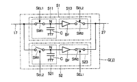
第1表示体10の基板11のうち表示領域A1からみて第2表示体20側(データ線駆動回路44とは反対側)には信号制御部52が配置される。信号制御部52は、第2表示体20のデータ線27の本数(あるいは第1表示体10のデータ線17の本数)に相当するn個の単位回路Q[1]〜Q[n]をX方向に配列した回路である。第j段目の単位回路Q[j]は、第1表示体10の第j列目のデータ線17と第2表示体20の第j列目のデータ線27(詳細には第j列目のデータ線27に接続されるフレキシブル配線基板75の配線)との間に介在する。制御回路70は、信号SEL1と信号SEL2とをn個の単位回路Q[1]〜Q[n]に対して共通に供給する。   A signal control unit 52 is disposed on the substrate 11 of the first display body 10 on the second display body 20 side (the side opposite to the data line driving circuit 44) when viewed from the display area A1. The signal control unit 52 converts n unit circuits Q [1] to Q [n] corresponding to the number of data lines 27 of the second display body 20 (or the number of data lines 17 of the first display body 10) to X It is a circuit arranged in the direction. The unit circuit Q [j] in the j-th stage includes the data line 17 in the j-th column of the first display body 10 and the data line 27 in the j-th column of the second display body 20 (more specifically, in the j-th column). And the flexible wiring board 75 connected to the data line 27). The control circuit 70 supplies the signal SEL1 and the signal SEL2 in common to the n unit circuits Q [1] to Q [n].

図2は、単位回路Q[j]の回路図である。図2に示すように、単位回路Q[j]は第1部分51と第2部分52とに区分される。第1部分51は保持部511と出力部513とを含み、第2部分52は保持部521と出力部523とを含む。保持部511および保持部521の各々はスイッチSW1と容量素子Cとで構成される。スイッチSW1は、第1表示体10における第j列目のデータ線17と接続点Nとの間に介在して両者の電気的な接続(導通/非導通)を制御する。容量素子Cは、接続点Nと接地線(または他の定電位線)との間に介挿される。一方、出力部513および出力部523の各々はバッファ回路BFとスイッチSW2とで構成される。バッファ回路BFの入力端は接続点Nに接続される。スイッチSW2は、バッファ回路BFの出力端と第2表示体20における第j列目のデータ線27との間に介在して両者の電気的な接続を制御する。第1部分51のスイッチSW1と第2部分52のスイッチSW2とは信号SEL1に応じて制御され、第1部分51のスイッチSW2と第2部分52のスイッチSW1とは信号SEL2に応じて制御される。   FIG. 2 is a circuit diagram of the unit circuit Q [j]. As shown in FIG. 2, the unit circuit Q [j] is divided into a first portion 51 and a second portion 52. The first part 51 includes a holding part 511 and an output part 513, and the second part 52 includes a holding part 521 and an output part 523. Each of the holding unit 511 and the holding unit 521 includes a switch SW1 and a capacitive element C. The switch SW1 is interposed between the j-th column data line 17 and the connection point N in the first display body 10, and controls the electrical connection (conduction / non-conduction) between the two. The capacitive element C is interposed between the connection point N and the ground line (or other constant potential line). On the other hand, each of the output unit 513 and the output unit 523 includes a buffer circuit BF and a switch SW2. The input terminal of the buffer circuit BF is connected to the connection point N. The switch SW2 is interposed between the output terminal of the buffer circuit BF and the data line 27 of the j-th column in the second display body 20, and controls the electrical connection between them. The switch SW1 of the first part 51 and the switch SW2 of the second part 52 are controlled according to the signal SEL1, and the switch SW2 of the first part 51 and the switch SW1 of the second part 52 are controlled according to the signal SEL2. .

次に、表示装置100の動作を説明する。画像の表示先として第1表示体10を指定した場合、制御回路70は、信号SEL1および信号SEL2の双方をローレベルに設定する。したがって、単位回路Q[1]〜Q[n]の各々において第1部分51および第2部分52の双方におけるスイッチSW1およびスイッチSW2がオフ状態となる。すなわち、第2表示体20のデータ線27は第1表示体10のデータ線17から電気的に切り離される。以上の状態において、走査線駆動回路42は、走査信号YA[1]〜YA[m]を出力することで第1表示体10のm本の走査線15の各々を順次に選択する一方、データ線駆動回路44は、第1表示体10の各画素P1の階調データに応じたデータ信号D[1]〜D[n]をn本のデータ線17の各々に出力する。したがって、データ信号D[1]〜D[n]に応じた電圧が第1表示体10の各画素P1の電気光学素子34に印加され、第1表示体10の表示領域A1には階調データに応じた画像が表示される。   Next, the operation of the display device 100 will be described. When the first display body 10 is designated as the image display destination, the control circuit 70 sets both the signal SEL1 and the signal SEL2 to a low level. Accordingly, in each of the unit circuits Q [1] to Q [n], the switches SW1 and SW2 in both the first portion 51 and the second portion 52 are turned off. That is, the data line 27 of the second display body 20 is electrically disconnected from the data line 17 of the first display body 10. In the above state, the scanning line driving circuit 42 sequentially selects each of the m scanning lines 15 of the first display body 10 by outputting the scanning signals YA [1] to YA [m], while the data The line drive circuit 44 outputs data signals D [1] to D [n] corresponding to the gradation data of each pixel P1 of the first display body 10 to each of the n data lines 17. Therefore, a voltage corresponding to the data signals D [1] to D [n] is applied to the electro-optic element 34 of each pixel P1 of the first display body 10, and the gradation data is displayed in the display area A1 of the first display body 10. An image corresponding to is displayed.

画像の表示先として第2表示体20を指定した場合、制御回路70は、図3に示すように、単位期間TUを周期として変動する信号SEL1および信号SEL2を生成して信号制御部52に出力する。信号SEL1と信号SEL2とはレベルを反転させた関係にある。すなわち、信号SEL1は、各単位期間TUのうち前半の期間T1にてハイレベルを維持するとともに後半の期間T2にてローレベルを維持し、信号SEL2は、各単位期間TUのうち前半の期間T1にてローレベルを維持するとともに後半の期間T2にてハイレベルを維持する。一方、走査線駆動回路42は第2表示体20のm本の走査線25の各々を順次に選択し、データ線駆動回路44は、第2表示体20の各画素P2の階調データに応じたデータ信号D[1]〜D[n]をn本のデータ線17の各々に出力する。   When the second display body 20 is designated as an image display destination, the control circuit 70 generates the signal SEL1 and the signal SEL2 that change with the unit period TU as a cycle and outputs the signal SEL1 to the signal control unit 52 as shown in FIG. To do. The signal SEL1 and the signal SEL2 have a relationship in which the levels are inverted. That is, the signal SEL1 maintains a high level in the first half period T1 of each unit period TU and maintains a low level in the second half period T2, and the signal SEL2 is in the first half period T1 of each unit period TU. The low level is maintained and the high level is maintained in the second half period T2. On the other hand, the scanning line driving circuit 42 sequentially selects each of the m scanning lines 25 of the second display body 20, and the data line driving circuit 44 responds to the gradation data of each pixel P2 of the second display body 20. The data signals D [1] to D [n] are output to each of the n data lines 17.

図3には、単位回路Q[j]の第1部分51および第2部分52の各々における容量素子Cが保持する電圧(接続点Nの電圧)がデータ信号D[j]の電圧の波形とともに図示されている。単位期間TUの期間T1においては、信号SEL1がハイレベルに設定されることで単位回路Q[1]〜Q[n]の各々における第1部分51のスイッチSW1がオン状態に制御される。したがって、第j列目のデータ線17に供給されたデータ信号D[j]が単位回路Q[j]における第1部分51の容量素子Cに保持される。容量素子Cに保持されたデータ信号D[j]は、図3に示すように、信号SEL1がローレベルに遷移することでスイッチSW1がオフ状態に変化する単位期間TUの期間T2でも維持される。そして、期間T2においては、信号SEL2がハイレベルに設定されることで各単位回路Q[j]における第1部分51のスイッチSW2がオン状態に制御される。したがって、直前の期間T1にて容量素子Cに保持されたデータ信号D[j]が、バッファ回路BFによる波形の整形後にスイッチSW2を経由して第2表示体20の第j列目のデータ線27に出力される。   In FIG. 3, the voltage (voltage at the connection point N) held by the capacitive element C in each of the first part 51 and the second part 52 of the unit circuit Q [j] is shown along with the voltage waveform of the data signal D [j]. It is shown in the figure. In the period T1 of the unit period TU, the signal SEL1 is set to the high level, so that the switch SW1 of the first portion 51 in each of the unit circuits Q [1] to Q [n] is controlled to be in the on state. Therefore, the data signal D [j] supplied to the data line 17 in the jth column is held in the capacitive element C of the first portion 51 in the unit circuit Q [j]. As shown in FIG. 3, the data signal D [j] held in the capacitive element C is maintained even during the period T2 of the unit period TU in which the switch SW1 is turned off by the signal SEL1 transitioning to the low level. . In the period T2, the signal SEL2 is set to a high level, so that the switch SW2 of the first portion 51 in each unit circuit Q [j] is controlled to be in an on state. Therefore, the data signal D [j] held in the capacitive element C in the immediately preceding period T1 is subjected to waveform shaping by the buffer circuit BF and then the data line in the jth column of the second display body 20 via the switch SW2. 27 is output.

一方、単位回路Q[j]の第2部分52においては、信号SEL2がハイレベルに設定される単位期間TUの期間T2にてスイッチSW1がオン状態となることでデータ信号D[j]が容量素子Cに保持される。そして、直後の期間T1にて信号SEL1がハイレベルに設定されることでスイッチSW2がオン状態に変化するから、図3のように容量素子Cに保持されたデータ信号D[j]が期間T1にて第2表示体20の第j列目のデータ線27に出力される。すなわち、単位回路Q[j]の第1部分51がデータ線17のデータ信号D[j]を保持するとともに第2部分52が容量素子Cのデータ信号D[j]をデータ線27に出力する動作と、単位回路Q[j]の第1部分51が容量素子CのデータD[j]をデータ線27に出力するとともに第2部分52がデータ線17のデータ信号D[j]を保持する動作とが、単位期間TUの半分の時間長を周期として順次に反復される。   On the other hand, in the second portion 52 of the unit circuit Q [j], the data signal D [j] has a capacitance when the switch SW1 is turned on in the period T2 of the unit period TU in which the signal SEL2 is set to the high level. It is held by element C. Then, since the signal SEL1 is set to the high level in the immediately following period T1, the switch SW2 is turned on, so that the data signal D [j] held in the capacitor C as shown in FIG. Is output to the data line 27 of the j-th column of the second display body 20. That is, the first portion 51 of the unit circuit Q [j] holds the data signal D [j] of the data line 17 and the second portion 52 outputs the data signal D [j] of the capacitive element C to the data line 27. In operation, the first portion 51 of the unit circuit Q [j] outputs the data D [j] of the capacitive element C to the data line 27 and the second portion 52 holds the data signal D [j] of the data line 17. The operation is sequentially repeated with a half time length of the unit period TU as a period.

以上のように第2表示体20のn本のデータ線27にデータ信号D[1]〜D[n]を出力する動作に並行して第2表示体20のm本の走査線25の各々を走査線駆動回路42が順次に選択するから、データ信号D[1]〜D[n]に応じた電圧が第2表示体20の各画素P2の電気光学素子34に印加され、第2表示体20の表示領域A2には階調データに応じた画像が表示される。なお、以上の説明から理解されるように、第2表示体20に供給されるデータ信号D[j]は第1表示体10におけるデータ信号D[j]と比較して単位期間TUの半分の時間長だけ遅延した信号となる。したがって、走査線駆動回路42は、第2表示体20に供給されるデータ信号D[j]の位相に合致するように走査信号YB[1]〜YB[m]を生成する。   As described above, each of the m scanning lines 25 of the second display body 20 in parallel with the operation of outputting the data signals D [1] to D [n] to the n data lines 27 of the second display body 20. Are sequentially selected by the scanning line driving circuit 42, a voltage corresponding to the data signals D [1] to D [n] is applied to the electro-optic element 34 of each pixel P2 of the second display body 20, and the second display. In the display area A2 of the body 20, an image corresponding to the gradation data is displayed. As can be understood from the above description, the data signal D [j] supplied to the second display body 20 is half the unit period TU compared to the data signal D [j] in the first display body 10. The signal is delayed by the length of time. Accordingly, the scanning line driving circuit 42 generates the scanning signals YB [1] to YB [m] so as to match the phase of the data signal D [j] supplied to the second display body 20.

以上に説明したように本形態においては、第1表示体10と第2表示体20とでデータ線駆動回路44が共用されるから、第1表示体10および第2表示体20の各々に別個のデータ線駆動回路44を配置する必要がない。したがって、表示装置100にて消費される電力や表示装置100の製造に必要なコストを削減することが可能である。また、データ線駆動回路44には相補型のトランジスタが必要であるところ、本形態においては第2表示体20にデータ線駆動回路44を配置する必要がないから、第2表示体20の基板21に形成されるトランジスタ(例えば画素P2のトランジスタ)の導電型はnチャネル型およびpチャネル型の一方のみで足りる。したがって、第2表示体20の基板21に相補型のトランジスタを形成する場合と比較して第2表示体20の製造を簡素化することが可能である。   As described above, in this embodiment, since the data line driving circuit 44 is shared by the first display body 10 and the second display body 20, each of the first display body 10 and the second display body 20 is separately provided. It is not necessary to arrange the data line driving circuit 44 of the first data line. Therefore, it is possible to reduce the power consumed by the display device 100 and the cost required for manufacturing the display device 100. The data line driving circuit 44 requires a complementary transistor. In this embodiment, the data line driving circuit 44 does not need to be disposed on the second display body 20, and thus the substrate 21 of the second display body 20. Only one of the n-channel type and the p-channel type is sufficient as the conductivity type of the transistor (for example, the transistor of the pixel P2) formed in (1). Therefore, it is possible to simplify the manufacture of the second display body 20 as compared with the case where a complementary transistor is formed on the substrate 21 of the second display body 20.

また、第2表示体20に画像を表示する場合に、第1表示体10のデータ線17にデータ線駆動回路44から出力されたデータ信号D[j]は、単位回路Q[j]に保持されたうえで第2表示体20のデータ線27に出力される。したがって、データ線17とデータ線27とが直接に接続された構成と比較して、データ線駆動回路44での負荷が軽減されるという利点がある。さらに、本形態においては、単位回路Q[j]の第1部分51がデータ線27にデータ信号D[j]を出力する期間T2では第2部分52がデータ信号D[j]をデータ線17から取込み、第2部分52がデータ線27にデータ信号D[j]を出力する期間T1では第1部分51がデータ信号D[j]をデータ線17から取込む。以上の構成によれば、容量素子Cにおけるデータ信号D[j]の保持のために充分な時間を確保できるという利点がある。したがって、バッファ回路BFの駆動能力が低い場合(例えば第1表示体10の基板11上に直接に形成された薄膜トランジスタでバッファ回路BFを構成した場合)であっても確実にデータ信号D[j]をデータ線27に出力できる。   Further, when an image is displayed on the second display body 20, the data signal D [j] output from the data line driving circuit 44 to the data line 17 of the first display body 10 is held in the unit circuit Q [j]. Then, the data is output to the data line 27 of the second display body 20. Therefore, there is an advantage that the load on the data line driving circuit 44 is reduced as compared with the configuration in which the data line 17 and the data line 27 are directly connected. Further, in this embodiment, in the period T2 in which the first portion 51 of the unit circuit Q [j] outputs the data signal D [j] to the data line 27, the second portion 52 outputs the data signal D [j] to the data line 17. The first portion 51 captures the data signal D [j] from the data line 17 in the period T1 during which the second portion 52 outputs the data signal D [j] to the data line 27. According to the above configuration, there is an advantage that a sufficient time can be secured for holding the data signal D [j] in the capacitive element C. Therefore, even when the driving capability of the buffer circuit BF is low (for example, when the buffer circuit BF is configured by a thin film transistor formed directly on the substrate 11 of the first display body 10), the data signal D [j] is surely obtained. Can be output to the data line 27.

なお、以上の構成においては第1表示体10の各走査線15および第2表示体20の各走査線25を第1表示体10上の走査線駆動回路42で駆動したが、図4に示すように、各走査線15を選択する走査線駆動回路42Aが第1表示体10に配置されるとともに各走査線25を選択する走査線駆動回路42Bが第2表示体20に配置される構成も採用される。   In the above configuration, each scanning line 15 of the first display body 10 and each scanning line 25 of the second display body 20 are driven by the scanning line drive circuit 42 on the first display body 10, but are shown in FIG. As described above, the scanning line driving circuit 42A for selecting each scanning line 15 is arranged on the first display body 10 and the scanning line driving circuit 42B for selecting each scanning line 25 is also arranged on the second display body 20. Adopted.

<B:第2実施形態>
次に、本発明の第2実施形態について説明する。第1実施形態ではデータ線17とデータ線27との間に単位回路Q[1]〜Q[n](信号制御部52)を介在させた。本形態においては、第1表示体10の走査線15および第2表示体20の走査線25についても同様の構成を採用する。なお、以下の各形態において作用や機能が第1実施形態と同等である要素については、以上と同じ符号を付して各々の詳細な説明を適宜に省略する。
<B: Second Embodiment>
Next, a second embodiment of the present invention will be described. In the first embodiment, unit circuits Q [1] to Q [n] (signal control unit 52) are interposed between the data line 17 and the data line 27. In the present embodiment, the same configuration is adopted for the scanning lines 15 of the first display body 10 and the scanning lines 25 of the second display body 20. In addition, about the element in which an effect | action and a function are equivalent to 1st Embodiment in each following form, the same code | symbol as the above is attached | subjected and each detailed description is abbreviate | omitted suitably.

図5は、第1表示体10の各走査線15や第2表示体20の各走査線25と走査線駆動回路42との関係を示すブロック図である。各データ線17や各データ線27とデータ線駆動回路44および信号制御部52との関係は第1実施形態と同様であるため図5では図示を省略した。図5に示すように、第1表示体10の基板11のうち第2表示体20側(走査線駆動回路42とは反対側)の周縁には信号制御部54が配置される。信号制御部54は、第2表示体20の走査線25の総数(第1表示体10の走査線15の総数)に相当するm個の単位回路R[1]〜R[m]をX方向に配列した回路である。単位回路R[1]〜R[m]の各々は、図2に例示した単位回路Q[j]と同様に第1部分51と第2部分52とで構成され、制御回路70から供給される信号SEL1および信号SEL2に応じて制御される。もっとも、信号制御部52および信号制御部54の各々を別系統の信号で制御してもよい。   FIG. 5 is a block diagram showing the relationship between each scanning line 15 of the first display body 10 and each scanning line 25 of the second display body 20 and the scanning line driving circuit 42. Since the relationship between each data line 17 or each data line 27 and the data line drive circuit 44 and the signal control unit 52 is the same as that in the first embodiment, the illustration is omitted in FIG. As shown in FIG. 5, a signal control unit 54 is disposed on the periphery of the substrate 11 of the first display body 10 on the second display body 20 side (the side opposite to the scanning line driving circuit 42). The signal control unit 54 supplies m unit circuits R [1] to R [m] corresponding to the total number of scanning lines 25 of the second display body 20 (total number of scanning lines 15 of the first display body 10) in the X direction. It is a circuit arranged in. Each of the unit circuits R [1] to R [m] is composed of a first portion 51 and a second portion 52 as in the unit circuit Q [j] illustrated in FIG. Control is performed according to the signals SEL1 and SEL2. But you may control each of the signal control part 52 and the signal control part 54 with the signal of another system | strain.

信号制御部54における第i段目(i=1〜m)の単位回路R[i]は、第1表示体10における第i行目の走査線15と第2表示体20における第i行目の走査線25との間に介在する。走査線駆動回路42が生成および出力する走査信号Y[1]〜Y[m]は、第1表示体10のm本の走査線15の各々に供給されるとともに信号制御部54のm個の単位回路R[1]〜R[m]の各々にも供給される。   The unit circuit R [i] of the i-th stage (i = 1 to m) in the signal control unit 54 includes the i-th scanning line 15 in the first display body 10 and the i-th row in the second display body 20. Between the scanning line 25 and the scanning line 25. Scan signals Y [1] to Y [m] generated and output by the scan line driving circuit 42 are supplied to each of the m scan lines 15 of the first display body 10 and m signals of the signal control unit 54. It is also supplied to each of the unit circuits R [1] to R [m].

単位回路R[i]の第1部分51は、走査線15に供給される走査信号Y[i]を単位期間TUの期間T1にて容量素子Cに保持し、期間T2にてバッファ回路BFおよびスイッチSW2から走査線25に出力する。単位回路R[i]の第2部分52は、走査線15に供給される走査信号Y[i]を単位期間TUの期間T2にて容量素子Cに保持し、直後の期間T1にてバッファ回路BFからスイッチSW2を介して走査線25に出力する。すなわち、第1表示体10の各走査線15に供給される走査信号Y[1]〜Y[m]が信号制御部54にて単位期間TUの半分の時間長だけ遅延したうえで第2表示体20の各走査線25に供給される。データ線駆動回路44および信号制御部52は第1実施形態と同様に動作するから、本形態においては第1表示体10の表示領域A1と第2表示体20の表示領域A2とに同等の画像が並行して表示される。   The first portion 51 of the unit circuit R [i] holds the scanning signal Y [i] supplied to the scanning line 15 in the capacitive element C during the period T1 of the unit period TU, and the buffer circuit BF and the buffer circuit BF during the period T2. The signal is output from the switch SW2 to the scanning line 25. The second portion 52 of the unit circuit R [i] holds the scanning signal Y [i] supplied to the scanning line 15 in the capacitive element C in the period T2 of the unit period TU, and the buffer circuit in the immediately following period T1. The signal is output from BF to the scanning line 25 via the switch SW2. That is, after the scanning signals Y [1] to Y [m] supplied to the scanning lines 15 of the first display body 10 are delayed by the signal controller 54 by a time length that is half the unit period TU, the second display is performed. It is supplied to each scanning line 25 of the body 20. Since the data line driving circuit 44 and the signal control unit 52 operate in the same manner as in the first embodiment, in this embodiment, images equivalent to the display area A1 of the first display body 10 and the display area A2 of the second display body 20 are displayed. Are displayed in parallel.

以上に説明したように本形態においては、第1表示体10の走査線15に出力された走査信号Y[i]が単位回路R[i]に保持されたうえで第2表示体20の走査線25に出力される。したがって、例えば走査線15と走査線25とが直接に接続された構成と比較して、走査線駆動回路42の負荷が軽減されるという利点がある。さらに、単位回路R[i]における第1部分51と第2部分52とが交互に走査信号Y[i]を出力するから、容量素子Cに走査信号Y[i]を保持させる時間を充分に確保することができる。したがって、単位回路R[i]におけるバッファ回路BFの駆動能力が低い場合(例えば第1表示体10の基板11上に直接に形成された薄膜トランジスタでバッファ回路BFを構成した場合)であっても確実に走査信号Y[i]を走査線25に出力できる。   As described above, in this embodiment, the scanning signal Y [i] output to the
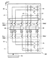
 scanning line 15 of the first display body 10 is held in the unit circuit R [i] and then the second display body 20 is scanned. Output on line 25. Therefore, for example, there is an advantage that the load on the scanning line driving circuit 42 is reduced as compared with a configuration in which the scanning lines 15 and 25 are directly connected. Furthermore, since the first portion 51 and the second portion 52 in the unit circuit R [i] alternately output the scanning signal Y [i], a sufficient time is allowed for the capacitive element C to hold the scanning signal Y [i]. Can be secured. Therefore, even when the driving capability of the buffer circuit BF in the unit circuit R [i] is low (for example, when the buffer circuit BF is configured by a thin film transistor formed directly on the substrate 11 of the first display body 10), it is reliable. In addition, the scanning signal Y [i] can be output to the scanning line 25.

<C:第3実施形態>
図6は、本発明の第3実施形態に係る表示装置100の構成を示すブロック図である。図6に示すように、第1表示体10の基板11の表面のうち表示領域A1からみて第2表示体20側(すなわち表示領域A1と表示領域A2との間隙)に走査線駆動回路42およびデータ線駆動回路44が配置される。基板11のうちデータ線駆動回路44と表示領域A1との間隙にはn個のスイッチSWa1がX方向に配列する。第j段目のスイッチSWa1は、データ線駆動回路44におけるデータ信号D[j]の出力端と第1表示体10の第j列目のデータ線17との間に介在して両者の電気的な接続を制御する。基板11のうちデータ線駆動回路44を挟んで表示領域A1とは反対側の領域にはn個のスイッチSWa2がX方向に配列する。第j段目のスイッチSWa2は、データ線駆動回路44におけるデータ信号D[j]の出力端と第2表示体20の第j列目のデータ線27との間に介在して両者の電気的な接続を制御する。
<C: Third Embodiment>
FIG. 6 is a block diagram showing the configuration of the display device 100 according to the third embodiment of the present invention. As shown in FIG. 6, the scanning line driving circuit 42 and the second display body 20 side of the surface of the substrate 11 of the first display body 10 as viewed from the display area A1 (that is, the gap between the display area A1 and the display area A2) A data line driving circuit 44 is arranged. In the substrate 11, n switches SWa 1 are arranged in the X direction in the gap between the data line driving circuit 44 and the display area A 1. The j-th stage switch SWa1 is interposed between the output end of the data signal D [j] in the data line driving circuit 44 and the j-th column data line 17 of the first display body 10, and electrically The correct connection. In the area of the substrate 11 opposite to the display area A1 across the data line driving circuit 44, n switches SWa2 are arranged in the X direction. The j-th stage switch SWa2 is interposed between the output terminal of the data signal D [j] in the data line driving circuit 44 and the j-th column data line 27 of the second display body 20, and electrically The correct connection.

基板11のうち走査線駆動回路42と表示領域A1との間隙にはm個のスイッチSWb1がX方向に配列する。第i段目のスイッチSWb1は、走査線駆動回路42における走査信号Y[i]の出力端と第1表示体10の第i行目の走査線15との間に介在して両者の電気的な接続を制御する。基板11のうち走査線駆動回路42を挟んで表示領域A1とは反対側の領域にはm個のスイッチSWb2がX方向に配列する。第i段目のスイッチSWb2は、走査線駆動回路42における走査信号Y[i]の出力端と第2表示体20の第i行目の走査線25との間に介在して両者の電気的な接続を制御する。各スイッチ(SWa1,SWa2,SWb1,SWb2)は、例えば基板11の表面に直接に形成された薄膜トランジスタである。   In the gap between the scanning line driving circuit 42 and the display area A1 in the substrate 11, m switches SWb1 are arranged in the X direction. The i-th stage switch SWb1 is interposed between the output terminal of the scanning signal Y [i] in the scanning line driving circuit 42 and the i-th scanning line 15 of the first display body 10, and electrically The correct connection. In the area of the substrate 11 opposite to the display area A1 across the scanning line driving circuit 42, m switches SWb2 are arranged in the X direction. The i-th stage switch SWb2 is interposed between the output terminal of the scanning signal Y [i] in the scanning line driving circuit 42 and the i-th scanning line 25 of the second display body 20, and electrically The correct connection. Each switch (SWa1, SWa2, SWb1, SWb2) is, for example, a thin film transistor formed directly on the surface of the substrate 11.

各スイッチSWa1および各スイッチSWb1は信号SEL1に応じて動作し、各スイッチSWa2および各スイッチSWb2は信号SEL2に応じて動作する。画像の表示先として第1表示体10を指定した場合、制御回路70は、各スイッチSWa1および各スイッチSWb1がオン状態となるように信号SEL1を設定するとともに各スイッチSWa2および各スイッチSWb2がオフ状態となるように信号SEL2を設定する。以上の状態においては、走査線駆動回路42の出力する走査信号Y[1]〜Y[m]が第1表示体10の各走査線15に供給されるとともにデータ線駆動回路44の出力するデータ信号D[1]〜D[n]が第1表示体10の各データ線17に供給される。したがって、第1表示体10の表示領域A1に画像が表示される。走査信号Y[1]〜Y[m]やデータ信号D[1]〜D[n]は第2表示体20に供給されないから、第2表示体20の表示領域A2に画像は表示されない。   Each switch SWa1 and each switch SWb1 operate according to the signal SEL1, and each switch SWa2 and each switch SWb2 operate according to the signal SEL2. When the first display body 10 is designated as an image display destination, the control circuit 70 sets the signal SEL1 so that each switch SWa1 and each switch SWb1 is turned on, and each switch SWa2 and each switch SWb2 is turned off. The signal SEL2 is set so that In the above state, the scanning signals Y [1] to Y [m] output from the scanning line driving circuit 42 are supplied to the scanning lines 15 of the first display body 10, and the data output from the data line driving circuit 44 is output. Signals D [1] to D [n] are supplied to the data lines 17 of the first display body 10. Accordingly, an image is displayed in the display area A1 of the first display body 10. Since the scanning signals Y [1] to Y [m] and the data signals D [1] to D [n] are not supplied to the second display body 20, no image is displayed on the display area A2 of the second display body 20.

一方、画像の表示先として第2表示体20を指定した場合、制御回路70は、各スイッチSWa2および各スイッチSWb2がオン状態となるように信号SEL2を設定するとともに各スイッチSWa1および各スイッチSWb1がオフ状態となるように信号SEL1を設定する。したがって、走査信号Y[1]〜Y[m]が各走査線25のみに供給されるとともに、データ信号D[1]〜D[n]が各データ線27のみに供給される。したがって、画像は第2表示体20の表示領域A2のみに表示される。   On the other hand, when the second display body 20 is designated as the image display destination, the control circuit 70 sets the signal SEL2 so that each switch SWa2 and each switch SWb2 is turned on, and each switch SWa1 and each switch SWb1 is set. The signal SEL1 is set so as to be turned off. Accordingly, the scanning signals Y [1] to Y [m] are supplied only to the scanning lines 25, and the data signals D [1] to D [n] are supplied only to the data lines 27. Therefore, the image is displayed only in the display area A2 of the second display body 20.

以上に説明したように本形態においては、各走査線15および各走査線25の一方のみに走査信号Y[1]〜Y[m]が供給されるから、例えば走査線15と走査線25とが接続された構成(走査信号Y[i]が走査線15および走査線25の双方に出力される構成)と比較して走査線駆動回路42の負荷が軽減される。同様に、各データ線17および各データ線27の一方のみにデータ信号D[1]〜D[n]が供給されるから、データ線17とデータ線27とが接続された構成(データ信号D[j]がデータ線17およびデータ線27の双方に出力される構成)と比較してデータ線駆動回路44の負荷が軽減される。しかも、本形態においては、第1実施形態の信号制御部52や第2実施形態の信号制御部54を配置する必要がない。また、走査線駆動回路42が各走査線15と各走査線25との間に配置されるとともにデータ線駆動回路44が各データ線17と各データ線27との間に配置されるから、第1表示体10を駆動する場合と第2表示体20を駆動する場合とで走査線駆動回路42やデータ線駆動回路44の負荷が均一化されるという利点がある。   As described above, in this embodiment, since the scanning signals Y [1] to Y [m] are supplied to only one of the scanning lines 15 and the scanning lines 25, for example, the scanning lines 15 and 25 Compared with the configuration in which the scanning signal Y [i] is output to both the scanning line 15 and the scanning line 25, the load on the scanning line driving circuit 42 is reduced. Similarly, since data signals D [1] to D [n] are supplied to only one of each data line 17 and each data line 27, the data line 17 and the data line 27 are connected (data signal D). Compared with a configuration in which [j] is output to both the data line 17 and the data line 27), the load on the data line driving circuit 44 is reduced. In addition, in this embodiment, it is not necessary to arrange the signal control unit 52 of the first embodiment and the signal control unit 54 of the second embodiment. Further, since the scanning line driving circuit 42 is disposed between each scanning line 15 and each scanning line 25 and the data line driving circuit 44 is disposed between each data line 17 and each data line 27, There is an advantage that the load on the scanning line driving circuit 42 and the data line driving circuit 44 is equalized when the first display body 10 is driven and when the second display body 20 is driven.

<D:第4実施形態>
図7は、本発明の第4実施形態に係る表示装置100のブロック図である。図7に示すように第1表示体10と第2表示体20とはX方向に配置されるとともにフレキシブル配線基板75を介して電気的に接続される。第1表示体10の基板11にはデータ線駆動回路44Aが配置される。データ線駆動回路44Aは、第1表示体10のn本のデータ線17の各々にデータ信号DA[1]〜DA[n]を出力する。同様に、第2表示体20の基板21には、第2表示体20のn本のデータ線27の各々にデータ信号DB[1]〜DB[n]を出力するデータ線駆動回路44Bが配置される。
<D: Fourth Embodiment>
FIG. 7 is a block diagram of a display device 100 according to the fourth embodiment of the present invention. As shown in FIG. 7, the first display body 10 and the second display body 20 are arranged in the X direction and are electrically connected via a flexible wiring board 75. A data line driving circuit 44A is disposed on the substrate 11 of the first display body 10. The data line driving circuit 44A outputs data signals DA [1] to DA [n] to each of the n data lines 17 of the first display body 10. Similarly, a data line driving circuit 44B that outputs data signals DB [1] to DB [n] to each of the n data lines 27 of the second display body 20 is disposed on the substrate 21 of the second display body 20. Is done.

第1表示体10の基板11のうち表示領域A1からみて第2表示体20側には走査線駆動回路42が配置される。走査線駆動回路42は、第3実施形態と同様にm系統の走査信号Y[1]〜Y[m]を生成して出力する。第1表示体10の第i行目の走査線15および第2表示体20の第i行目の走査線25はともに走査線駆動回路42における走査信号Y[i]の出力端に電気的に接続される。したがって、第i行目の走査線15と第i行目の走査線25とに対して共通の走査信号Y[i]が供給される。   A scanning line driving circuit 42 is disposed on the second display body 20 side of the substrate 11 of the first display body 10 as viewed from the display area A1. The scanning line driving circuit 42 generates and outputs m systems of scanning signals Y [1] to Y [m] as in the third embodiment. Both the i-th scanning line 15 of the first display body 10 and the i-th scanning line 25 of the second display body 20 are electrically connected to the output terminal of the scanning signal Y [i] in the scanning line driving circuit 42. Connected. Accordingly, the common scanning signal Y [i] is supplied to the i-th scanning line 15 and the i-th scanning line 25.

制御回路70が画像の表示先として第1表示体10を指定すると、データ線駆動回路44Aが各データ線17にデータ信号DA[1]〜DA[n]を出力する。データ線駆動回路44Bは動作を停止するから、第1表示体10の表示領域A1のみに画像が表示される。一方、第2表示体20が指定されると、データ線駆動回路44Bのみが各データ線27にデータ信号DB[1]〜DB[n]を出力することで第2表示体20の表示領域A2に画像が表示される。また、制御回路70が第1表示体10および第2表示体20の双方を指定すると、データ線駆動回路44Aおよびデータ線駆動回路44Bの双方が動作することで表示領域A1および表示領域A2の双方に画像が表示される。   When the control circuit 70 designates the first display body 10 as an image display destination, the data line driving circuit 44A outputs data signals DA [1] to DA [n] to the data lines 17. Since the data line driving circuit 44B stops its operation, an image is displayed only in the display area A1 of the first display body 10. On the other hand, when the second display body 20 is designated, only the data line driving circuit 44B outputs the data signals DB [1] to DB [n] to the respective data lines 27, whereby the display area A2 of the second display body 20 is displayed. An image is displayed. When the control circuit 70 designates both the first display body 10 and the second display body 20, both the display area A1 and the display area A2 are operated by operating both the data line driving circuit 44A and the data line driving circuit 44B. An image is displayed.

以上に説明したように本形態においては、第1表示体10と第2表示体20とで走査線駆動回路42が共用されるから、第1表示体10および第2表示体20の各々に別個の走査線駆動回路42を配置する必要がない。したがって、表示装置100にて消費される電力や表示装置100の製造に必要なコストを削減することが可能である。また、走査線駆動回路42には相補型のトランジスタが必要であるところ、本形態においては第2表示体20に走査線駆動回路42を配置する必要がないから、第2表示体20の基板21に形成されるトランジスタの導電型をnチャネル型およびpチャネル型の一方のみとすることが可能である。したがって、第2表示体20の基板21に相補型のトランジスタを形成する場合と比較して第2表示体20の製造を簡素化することが可能である。   As described above, in the present embodiment, since the first display body 10 and the second display body 20 share the scanning line driving circuit 42, each of the first display body 10 and the second display body 20 is separately provided. It is not necessary to arrange the scanning line driving circuit 42. Therefore, it is possible to reduce the power consumed by the display device 100 and the cost required for manufacturing the display device 100. In addition, since the scanning line driving circuit 42 requires a complementary transistor, in this embodiment, since the scanning line driving circuit 42 does not need to be disposed on the second display body 20, the substrate 21 of the second display body 20. The conductivity type of the transistor formed in the transistor can be either n-channel or p-channel. Therefore, it is possible to simplify the manufacture of the second display body 20 as compared with the case where a complementary transistor is formed on the substrate 21 of the second display body 20.

<E:第5実施形態>
図8は、本発明の第5実施形態に係る表示装置100のブロック図である。図8に示すように、本形態の表示装置100は、検出体81および検出体82と信号処理部84と電源回路87とを第3実施形態の表示装置100に追加した構成である。検出体81は第1表示体10の基板11の表面に配置され、検出体82と信号処理部84と電源回路87とは第2表示体20の基板21の表面に配置される。信号処理部84や電源回路87は、例えば、基板21の表面に直接に形成された薄膜トランジスタで構成される。
<E: Fifth Embodiment>
FIG. 8 is a block diagram of a display device 100 according to the fifth embodiment of the present invention. As shown in FIG. 8, the display device 100 of this embodiment has a configuration in which a detection body 81, a detection body 82, a signal processing unit 84, and a power supply circuit 87 are added to the display device 100 of the third embodiment. The detection body 81 is disposed on the surface of the substrate 11 of the first display body 10, and the detection body 82, the signal processing unit 84, and the power supply circuit 87 are disposed on the surface of the substrate 21 of the second display body 20. The signal processing unit 84 and the power supply circuit 87 are composed of thin film transistors formed directly on the surface of the substrate 21, for example.

検出体81は、周囲の状態(第1表示体10の状態)に応じた検出信号を生成するセンサである。同様に、検出体82は、周囲の状態(第2表示体20の状態)に応じた検出信号を生成するセンサである。例えば、周囲の温度を検出する温度センサや周囲の光量を検出する照度センサが検出体81および検出体82として好適に採用される。なお、検出体81および検出体82の一方のみを設置してもよい。   The detection body 81 is a sensor that generates a detection signal corresponding to the surrounding state (the state of the first display body 10). Similarly, the detection body 82 is a sensor that generates a detection signal corresponding to the surrounding state (the state of the second display body 20). For example, a temperature sensor that detects the ambient temperature and an illuminance sensor that detects the amount of ambient light are suitably employed as the detection body 81 and the detection body 82. Only one of the detection body 81 and the detection body 82 may be installed.

信号処理部84は、検出体81や検出体82が生成した検出信号を処理する回路である。例えば、検出信号をデジタルデータに変換するA/D変換器や検出信号を増幅する増幅器が信号処理部84として採用される。信号処理部84による処理後の検出信号は制御回路70に出力される。制御回路70は、信号処理部84から供給される検出信号に基づいて走査線駆動回路42やデータ線駆動回路44の動作を制御する。例えば、検出信号のレベルが高い場合(例えば第1表示体10または第2表示体20の温度が高い場合や第1表示体10または第2表示体20の周囲の光量が多い場合)に各データ信号D[1]〜D[n]の電圧値を上昇または低下させるといった具合である。ただし、検出体81や検出体82による検出の結果に応じた制御の内容は任意である。   The signal processing unit 84 is a circuit that processes detection signals generated by the detection body 81 and the detection body 82. For example, an A / D converter that converts a detection signal into digital data and an amplifier that amplifies the detection signal are employed as the signal processing unit 84. A detection signal processed by the signal processing unit 84 is output to the control circuit 70. The control circuit 70 controls the operation of the scanning line driving circuit 42 and the data line driving circuit 44 based on the detection signal supplied from the signal processing unit 84. For example, when the level of the detection signal is high (for example, when the temperature of the first display body 10 or the second display body 20 is high or when the amount of light around the first display body 10 or the second display body 20 is large), each data For example, the voltage values of the signals D [1] to D [n] are increased or decreased. However, the content of the control according to the detection result by the detection body 81 or the detection body 82 is arbitrary.

図8の電源回路87は、表示装置100で使用される各種の電位(電源電位)を生成する回路(例えばチャージポンプ回路)である。電源回路87が生成した電位は、フレキシブル配線基板75上の配線を介して第1表示体10の走査線駆動回路42やデータ線駆動回路44に供給される。走査線駆動回路42やデータ線駆動回路44は、電源回路87から供給される電源電位を利用して動作する。また、電源回路87は、所定の基準電位を生成するとともに第1表示体10や第2表示体20の対向電極(共通電極)に供給する。   The power supply circuit 87 in FIG. 8 is a circuit (for example, a charge pump circuit) that generates various potentials (power supply potentials) used in the display device 100. The potential generated by the power supply circuit 87 is supplied to the scanning line driving circuit 42 and the data line driving circuit 44 of the first display body 10 via wiring on the flexible wiring board 75. The scanning line driving circuit 42 and the data line driving circuit 44 operate using the power supply potential supplied from the power supply circuit 87. The power supply circuit 87 generates a predetermined reference potential and supplies it to the counter electrode (common electrode) of the first display body 10 and the second display body 20.

以上に説明したように本形態においては、第1表示体10と第2表示体20とで信号処理部84や電源回路87が共用されるから、第1表示体10および第2表示体20の各々に信号処理部84や電源回路87を配置した構成と比較して、表示装置100にて消費される電力や表示装置100の製造に必要なコストを削減することが可能である。なお、図8においては第3実施形態を基礎とした形態を説明したが、信号処理部84や電源回路87を第1表示体10と第2表示体20とで共用する構成は、第1実施形態や第2実施形態や第4実施形態においても同様に採用される。   As described above, in the present embodiment, since the signal processing unit 84 and the power supply circuit 87 are shared by the first display body 10 and the second display body 20, the first display body 10 and the second display body 20. Compared with a configuration in which the signal processing unit 84 and the power supply circuit 87 are arranged, the power consumed by the display device 100 and the cost necessary for manufacturing the display device 100 can be reduced. In addition, although the form based on 3rd Embodiment was demonstrated in FIG. 8, the structure which shares the signal processing part 84 and the power supply circuit 87 with the 1st display body 10 and the 2nd display body 20 is 1st Embodiment. The same applies to the embodiment, the second embodiment, and the fourth embodiment.

<F:変形例>
以上の各形態には様々に変形される。具体的な変形の態様を以下に例示する。なお、以下の例示から2以上の態様を任意に選択して組合わせてもよい。
<F: Modification>
Various modifications can be made to the above embodiments. Specific modifications are exemplified below. Two or more aspects may be arbitrarily selected from the following examples and combined.

(1)変形例1
第1表示体10のデータ線17の本数と第2表示体20のデータ線27の本数とは相違してもよい。同様に、第1表示体10の走査線15の本数と第2表示体20の走査線25の本数とは相違してもよい。また、第1表示体10や第2表示体20とでサイズ(例えば表示領域や基板のサイズ)が相違する構成も採用される。なお、第1表示体10および第2表示体20のうちサイズの小さい表示体に走査線駆動回路42やデータ線駆動回路44を配置した構成が好適である。
(1) Modification 1
The number of data lines 17 of the first display body 10 may be different from the number of data lines 27 of the second display body 20. Similarly, the number of scanning lines 15 of the first display body 10 may be different from the number of scanning lines 25 of the second display body 20. A configuration in which the size (for example, the size of the display area or the substrate) is different between the first display body 10 and the second display body 20 is also adopted. A configuration in which the scanning line driving circuit 42 and the data line driving circuit 44 are arranged on a small display body of the first display body 10 and the second display body 20 is preferable.

(2)変形例2
第1実施形態および第2実施形態における信号制御部52や第2実施形態における信号制御部54は第2表示体20に設置されてもよい。同様に、第3実施形態における各スイッチ(SWa1,SWa2,SWb1,SWb2)が第2表示体20に配置された構成や第5実施形態における信号処理部84または電源回路87が第1表示体10に配置された構成も好適である。
(2) Modification 2
The signal control unit 52 in the first embodiment and the second embodiment and the signal control unit 54 in the second embodiment may be installed in the second display body 20. Similarly, each switch (SWa1, SWa2, SWb1, SWb2) in the third embodiment is arranged in the second display body 20, and the signal processing unit 84 or the power supply circuit 87 in the fifth embodiment is the first display body 10. A configuration arranged in the above is also suitable.

(3)変形例3
第1表示体10と第2表示体20とが一体をなす構成(例えばひとつの基板の表面に表示領域A1と表示領域A2とが画定された構成)も採用される。また、走査線駆動回路42(42A,42B)やデータ線駆動回路44(44A,44B)は、集積回路の形態で実装されてもよいし表示装置100に対して外付けされてもよい。
(3) Modification 3
A configuration in which the first display body 10 and the second display body 20 are integrated (for example, a configuration in which the display area A1 and the display area A2 are defined on the surface of one substrate) is also employed. Further, the scanning line driving circuit 42 (42A, 42B) and the data line driving circuit 44 (44A, 44B) may be mounted in the form of an integrated circuit or may be externally attached to the display device 100.

(4)変形例4
液晶容量は電気光学素子の例示に過ぎない。本発明に適用される電気光学素子について、自身が発光する自発光型と外光の透過率を変化させる非発光型との区別や、電流の供給によって駆動される電流駆動型と電界(電圧)の印加によって駆動される電圧駆動型との区別は不問である。例えば、有機EL(Electroluminescence)素子,無機EL素子,電界電子放出素子(FE(Field-Emission)素子),表面伝導型電子放出素子(SE(Surface conduction Electron emitter)素子),弾道電子放出素子(BS(Ballistic electron Emitting)素子),LED(Light Emitting Diode)素子,電気泳動素子、エレクトロクロミック素子など様々な電気光学素子を利用した表示装置に本発明は適用される。
(4) Modification 4
The liquid crystal capacitance is merely an example of an electro-optic element. The electro-optic element applied to the present invention is distinguished from a self-light-emitting type that emits light itself and a non-light-emitting type that changes the transmittance of external light, a current-driven type that is driven by current supply, and an electric field (voltage) There is no distinction from the voltage driven type driven by the application of. For example, an organic EL (Electroluminescence) element, an inorganic EL element, a field electron emission element (FE (Field-Emission) element), a surface conduction electron emission element (SE (Surface conduction Electron emitter) element), a ballistic electron emission element (BS) The present invention is applied to display devices using various electro-optical elements such as (Ballistic electron Emitting) elements, LED (Light Emitting Diode) elements, electrophoretic elements, and electrochromic elements.

<G:応用例>
次に、本発明に係る表示装置を利用した電子機器について説明する。図9ないし図11には、以上に説明した何れかの形態に係る表示装置100を利用した電子機器の形態が図示されている。
<G: Application example>
Next, an electronic apparatus using the display device according to the present invention will be described. FIGS. 9 to 11 show forms of electronic devices using the display device 100 according to any one of the forms described above.

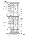
図9は、表示装置100を採用したモバイル型のパーソナルコンピュータの構成を示す斜視図である。パーソナルコンピュータ2000は、表示装置100と、電源スイッチ2001やキーボード2002が設置された本体部2010とを具備する。表示装置100が本体部2010に対して開いた状態では図9のように第1表示体10の表示領域A1を利用者が視認し、表示装置100が本体部2010に対して閉じられた状態では第2表示体20の表示領域A2を利用者が視認する。   FIG. 9 is a perspective view illustrating a configuration of a mobile personal computer that employs the display device 100. The personal computer 2000 includes the display device 100 and a main body 2010 on which a power switch 2001 and a keyboard 2002 are installed. When the display device 100 is opened with respect to the main body 2010, the user visually recognizes the display area A1 of the first display body 10 as shown in FIG. 9, and when the display device 100 is closed with respect to the main body 2010. The user visually recognizes the display area A2 of the second display body 20.

図10は、表示装置100を利用した携帯電話機の構成を示す斜視図である。携帯電話機3000は、複数の操作ボタン3001およびスクロールボタン3002と、以上の各形態に係る表示装置100とを具備する。表示装置100が操作ボタン3001に対して開かれた状態では図10のように第1表示体10の表示領域A1が利用者に視認され、表示装置100が操作ボタン3001側に閉じられた状態では第2表示体20の表示領域A2が利用者に視認される。   FIG. 10 is a perspective view illustrating a configuration of a mobile phone using the display device 100. A cellular phone 3000 includes a plurality of operation buttons 3001 and scroll buttons 3002, and the display device 100 according to each of the above modes. In the state where the display device 100 is opened with respect to the operation button 3001, the display area A1 of the first display body 10 is visually recognized by the user as shown in FIG. 10, and in the state where the display device 100 is closed to the operation button 3001 side. The display area A2 of the second display body 20 is visually recognized by the user.

図11は、表示装置100を利用した携帯情報端末(PDA:Personal Digital Assistants)の構成を示す斜視図である。携帯情報端末4000は、複数の操作ボタン4001および電源スイッチ4002と、以上の各形態に係る表示装置100とを具備する。第1表示体10(表示領域A1)は携帯情報端末4000の表面側(操作ボタン4001の配置側)に配置され、第2表示体20は背面側に配置される。電源スイッチ4002を操作すると、住所録やスケジュール帳といった様々な情報が表示装置100に表示される。   FIG. 11 is a perspective view showing a configuration of a personal digital assistant (PDA) using the display device 100. The portable information terminal 4000 includes a plurality of operation buttons 4001, a power switch 4002, and the display device 100 according to each of the above forms. The first display body 10 (display area A1) is arranged on the front side of the portable information terminal 4000 (the arrangement side of the operation buttons 4001), and the second display body 20 is arranged on the back side. When the power switch 4002 is operated, various information such as an address book and a schedule book are displayed on the display device 100.

なお、本発明に係る表示装置が適用される電子機器としては、図9から図11に例示した機器のほか、デジタルスチルカメラ、テレビ、ビデオカメラ、カーナビゲーション装置、ページャ、電子手帳、電子ペーパー、電卓、ワードプロセッサ、ワークステーション、テレビ電話、POS端末、プリンタ、スキャナ、複写機、ビデオプレーヤ、タッチパネルを備えた機器等などが挙げられる。   Note that examples of the electronic apparatus to which the display device according to the present invention is applied include the digital still camera, the television, the video camera, the car navigation apparatus, the pager, the electronic notebook, the electronic paper, in addition to the apparatuses illustrated in FIGS. Examples include calculators, word processors, workstations, videophones, POS terminals, printers, scanners, copiers, video players, devices equipped with touch panels, and the like.

本発明の第1実施形態に係る表示装置のブロック図である。1 is a block diagram of a display device according to a first embodiment of the present invention. 単位回路の回路図である。It is a circuit diagram of a unit circuit. 表示装置の動作を示すタイミングチャートである。It is a timing chart which shows operation | movement of a display apparatus. 第1実施形態の変形例に係る表示装置のブロック図である。It is a block diagram of the display apparatus concerning the modification of a 1st embodiment. 第2実施形態に係る表示装置の部分的な構成を示すブロック図である。It is a block diagram which shows the partial structure of the display apparatus which concerns on 2nd Embodiment. 第3実施形態に係る表示装置の構成を示すブロック図である。It is a block diagram which shows the structure of the display apparatus which concerns on 3rd Embodiment. 第4実施形態に係る表示装置の構成を示すブロック図である。It is a block diagram which shows the structure of the display apparatus which concerns on 4th Embodiment. 第5実施形態に係る表示装置の構成を示すブロック図である。It is a block diagram which shows the structure of the display apparatus which concerns on 5th Embodiment. 電子機器の形態(パーソナルコンピュータ)を示す斜視図である。It is a perspective view which shows the form (personal computer) of an electronic device. 電子機器の形態(携帯電話機)を示す斜視図である。It is a perspective view which shows the form (cellular phone) of an electronic device. 電子機器の形態(携帯情報端末)を示す斜視図である。It is a perspective view which shows the form (mobile information terminal) of an electronic device.

符号の説明Explanation of symbols

100……表示装置、10……第1表示体、20……第2表示体、15,25……走査線、17,27……データ線、A1,A2……表示領域、P1,P2……画素、42,42A,42B……走査線駆動回路、44,44A,44B……データ線駆動回路、52,54……信号制御部、51……第1部分、52……第2部分、511,521……保持部、513,523……出力部、SW1,SW2,SWa1,SWa2,SWb1,SWb2……スイッチ、70……制御回路。 DESCRIPTION OF SYMBOLS 100 ... Display apparatus, 10 ... 1st display body, 20 ... 2nd display body, 15, 25 ... Scanning line, 17, 27 ... Data line, A1, A2 ... Display area, P1, P2 ... ... Pixel, 42, 42A, 42B ... Scanning line drive circuit, 44, 44A, 44B ... Data line drive circuit, 52, 54 ... Signal control unit, 51 ... First part, 52 ... Second part, 511, 521 ... holding unit, 513, 523 ... output unit, SW1, SW2, SWa1, SWa2, SWb1, SWb2 ... switch, 70 ... control circuit.

Claims (9)

複数の第1配線の各々に画素が接続された第1表示体と、
複数の第2配線の各々に画素が接続された第2表示体と、
前記複数の第1配線を挟んで前記第2表示体とは反対側から前記複数の第1配線の各々に駆動信号を出力する駆動回路と、
前記第1表示体および前記第2表示体の一方に配置されて前記各第1配線と前記各第2配線との間に介在するとともに前記第1配線に供給された駆動信号を保持して前記第2配線に出力する複数の単位回路と
を具備する表示装置。
A first display body in which a pixel is connected to each of the plurality of first wirings;
A second display body in which a pixel is connected to each of the plurality of second wirings;
A drive circuit for outputting a drive signal to each of the plurality of first wirings from the opposite side of the second display body across the plurality of first wirings;
The first display body and the second display body are disposed between the first wirings and the second wirings and hold a drive signal supplied to the first wirings. And a plurality of unit circuits that output to the second wiring.
前記複数の単位回路の各々は、
前記第1配線に供給された駆動信号を複数の単位期間の各々における第1期間にて保持する第1保持手段と、前記第1保持手段が保持する駆動信号を前記複数の単位期間の各々における第2期間にて前記第2配線に出力する第1出力手段とを含む第1部分と、
前記第1配線に供給された駆動信号を前記複数の単位期間の各々における前記第2期間にて保持する第2保持手段と、前記第2保持手段が保持する駆動信号を前記複数の単位期間の各々における前記第1期間にて前記第2配線に出力する第2出力手段とを含む第2部分と
を有する請求項1の表示装置。
Each of the plurality of unit circuits is
First holding means for holding the drive signal supplied to the first wiring in a first period of each of a plurality of unit periods; and a drive signal held by the first holding means in each of the plurality of unit periods A first portion including first output means for outputting to the second wiring in a second period;
A second holding means for holding the drive signal supplied to the first wiring in the second period in each of the plurality of unit periods; and a drive signal held by the second holding means for the plurality of unit periods. 2. The display device according to claim 1, further comprising: a second portion including second output means for outputting to the second wiring in the first period in each.
複数の第1配線の各々に画素が接続された第1表示体と、
複数の第2配線の各々に画素が接続された第2表示体と、
前記第1表示体および前記第2表示体の一方において前記複数の第1配線と前記複数の第2配線との間に配置されて複数の駆動信号を出力する駆動回路と、
前記複数の第1配線の各々に対する前記各駆動信号の供給の可否を制御する複数の第1スイッチと、
前記複数の第2配線の各々に対する前記各駆動信号の供給の可否を制御する複数の第2スイッチと
を具備する表示装置。
A first display body in which a pixel is connected to each of the plurality of first wirings;
A second display body in which a pixel is connected to each of the plurality of second wirings;
A driving circuit arranged between the plurality of first wirings and the plurality of second wirings in one of the first display body and the second display body to output a plurality of driving signals;
A plurality of first switches for controlling whether or not each of the drive signals can be supplied to each of the plurality of first wirings;
A display device comprising: a plurality of second switches that control whether or not the drive signals can be supplied to each of the plurality of second wirings.
複数の第1配線の各々に画素が接続された第1表示体と、
複数の第2配線の各々に画素が接続された第2表示体と、
前記第1表示体および前記第2表示体の一方において前記複数の第1配線と前記複数の第2配線との間に配置されて前記各第1配線と前記各第2配線とに駆動信号を出力する駆動回路と
を具備する表示装置。
A first display body in which a pixel is connected to each of the plurality of first wirings;
A second display body in which a pixel is connected to each of the plurality of second wirings;
One of the first display body and the second display body is disposed between the plurality of first wirings and the plurality of second wirings and sends a drive signal to each of the first wirings and each of the second wirings. A display device comprising: a drive circuit for outputting.
前記駆動回路は、前記各画素に指定された階調に応じたデータ信号を前記駆動信号として出力するデータ線駆動回路である
請求項1から請求項4の何れかの表示装置。
5. The display device according to claim 1, wherein the drive circuit is a data line drive circuit that outputs a data signal corresponding to a gradation specified for each pixel as the drive signal.
前記駆動回路は、データ信号の供給の対象となる画素を選択する走査信号を前記駆動信号として出力する走査線駆動回路である
請求項1から請求項4の何れかの表示装置。
5. The display device according to claim 1, wherein the driving circuit is a scanning line driving circuit that outputs a scanning signal for selecting a pixel to which a data signal is supplied as the driving signal.
前記第1表示体および前記第2表示体の他方に配置されて電源電位を生成する電源回路を具備し、
前記駆動回路は、前記電源回路から電源電位の供給を受けて動作する
請求項1から請求項6の何れかの表示装置。
A power supply circuit that is disposed on the other of the first display body and the second display body and generates a power supply potential;
The display device according to claim 1, wherein the drive circuit operates by receiving supply of a power supply potential from the power supply circuit.
前記第1表示体または前記第2表示体の状態に応じた検出信号を生成する検出手段と、
前記第1表示体および前記第2表示体の他方に配置されて前記検出信号を処理する信号処理手段と
を具備し、
前記第1表示体および前記第2表示体の一方に配置された駆動回路は、前記信号処理手段による処理後の検出信号に基づいて前記駆動信号を生成する
請求項1から請求項7の何れかの表示装置。
Detection means for generating a detection signal according to a state of the first display body or the second display body;
Signal processing means disposed on the other of the first display body and the second display body for processing the detection signal;
8. The drive circuit disposed on one of the first display body and the second display body generates the drive signal based on a detection signal after processing by the signal processing means. Display device.
請求項1から請求項8の何れかの表示装置を具備する電子機器。
An electronic apparatus comprising the display device according to claim 1.
JP2007337829A 2007-12-27 2007-12-27 Display device and electronic apparatus Pending JP2009157258A (en)

Priority Applications (1)

Application Number Priority Date Filing Date Title
JP2007337829A JP2009157258A (en) 2007-12-27 2007-12-27 Display device and electronic apparatus

Applications Claiming Priority (1)

Application Number Priority Date Filing Date Title
JP2007337829A JP2009157258A (en) 2007-12-27 2007-12-27 Display device and electronic apparatus

Publications (1)

Publication Number Publication Date
JP2009157258A true JP2009157258A (en) 2009-07-16

Family

ID=40961318

Family Applications (1)

Application Number Title Priority Date Filing Date
JP2007337829A Pending JP2009157258A (en) 2007-12-27 2007-12-27 Display device and electronic apparatus

Country Status (1)

Country Link
JP (1) JP2009157258A (en)

Cited By (2)

* Cited by examiner, † Cited by third party
Publication number Priority date Publication date Assignee Title
CN105572986A (en) * 2016-01-29 2016-05-11 武汉华星光电技术有限公司 Double-panel display device
JP2020529620A (en) * 2017-08-08 2020-10-08 京東方科技集團股▲ふん▼有限公司Boe Technology Group Co.,Ltd. Scanning drive circuit and its drive method, display device

Cited By (4)

* Cited by examiner, † Cited by third party
Publication number Priority date Publication date Assignee Title
CN105572986A (en) * 2016-01-29 2016-05-11 武汉华星光电技术有限公司 Double-panel display device
CN105572986B (en) * 2016-01-29 2019-02-26 武汉华星光电技术有限公司 Double-side display device
US10288958B2 (en) 2016-01-29 2019-05-14 Wuhan China Star Optoelectronics Technology Co., Ltd Double-sided display devices
JP2020529620A (en) * 2017-08-08 2020-10-08 京東方科技集團股▲ふん▼有限公司Boe Technology Group Co.,Ltd. Scanning drive circuit and its drive method, display device

Similar Documents

Publication Publication Date Title
US8605027B2 (en) Shift register, display device having the same and method of driving the same
JP4882536B2 (en) Electronic circuit and electronic equipment
US20140043219A1 (en) Light emitting device, electronic apparatus, and method of driving light emitting device
WO2004051614A1 (en) Display and its driving method, and electronic device
US11037512B2 (en) Flexible display device
JP2011221070A (en) Light-emitting device and electronic apparatus, and method for driving light-emitting device
US11017730B2 (en) Display device and driving method of the same
JP4736614B2 (en) Signal transmission circuit, electro-optical device, and electronic apparatus
US11574571B2 (en) Display device having switching signal line between display regions
KR20120101305A (en) Electro-optical device and electronic apparatus
JP2010170009A (en) Display device and electronic apparatus
JP2009157258A (en) Display device and electronic apparatus
JP2007225653A (en) Electrooptical device and its driving method, and electronic equipment
JP2011085619A (en) Electro-optical device and electronic apparatus
CN116110341A (en) Pixel and display device comprising same
JP2005181975A (en) Pixel circuit, electro-optical device and electronic apparatus
KR100570772B1 (en) A driver for driving a display panel of a light emitting device, and a method thereof
JP2007096594A (en) Signal holding circuit, driver circuit, electrochemical device and electronic apparatus
JP5467568B2 (en) Electro-optical device, electronic apparatus, and driving method of electro-optical device
JP2007333930A (en) Electro-optical device and electronic device
JP4467900B2 (en) Driving method of light emitting device
JP2007114346A (en) Electrooptical apparatus and electronic apparatus
KR100813138B1 (en) Signal transmission circuit, electro-optical device, and electronic apparatus
JP2006003716A (en) Electronic circuit, its controlling method, electro-optic device, and electronic appliance
JP5094087B2 (en) Semiconductor device