US10714155B2 - Charge pump circuit with low reverse current and low peak current - Google Patents
Charge pump circuit with low reverse current and low peak current Download PDFInfo
- Publication number
- US10714155B2 US10714155B2 US16/247,584 US201916247584A US10714155B2 US 10714155 B2 US10714155 B2 US 10714155B2 US 201916247584 A US201916247584 A US 201916247584A US 10714155 B2 US10714155 B2 US 10714155B2
- Authority
- US
- United States
- Prior art keywords
- terminal
- type transistor
- coupled
- charge pump
- clock signal
- Prior art date
- Legal status (The legal status is an assumption and is not a legal conclusion. Google has not performed a legal analysis and makes no representation as to the accuracy of the status listed.)
- Active
Links
- 230000000630 rising effect Effects 0.000 claims abstract description 16
- 239000003990 capacitor Substances 0.000 claims description 34
- 230000000295 complement effect Effects 0.000 abstract description 11
- 230000008878 coupling Effects 0.000 description 3
- 238000010168 coupling process Methods 0.000 description 3
- 238000005859 coupling reaction Methods 0.000 description 3
- 230000000694 effects Effects 0.000 description 2
- 238000000034 method Methods 0.000 description 2
- 230000004075 alteration Effects 0.000 description 1
- 230000008901 benefit Effects 0.000 description 1
- 230000015556 catabolic process Effects 0.000 description 1
- 230000003111 delayed effect Effects 0.000 description 1
- 230000004048 modification Effects 0.000 description 1
- 238000012986 modification Methods 0.000 description 1
- 230000008569 process Effects 0.000 description 1
- 238000005086 pumping Methods 0.000 description 1
- 230000001360 synchronised effect Effects 0.000 description 1
Images


Classifications
-
- G—PHYSICS
- G11—INFORMATION STORAGE
- G11C—STATIC STORES
- G11C7/00—Arrangements for writing information into, or reading information out from, a digital store
- G11C7/06—Sense amplifiers; Associated circuits, e.g. timing or triggering circuits
- G11C7/065—Differential amplifiers of latching type
-
- H—ELECTRICITY
- H02—GENERATION; CONVERSION OR DISTRIBUTION OF ELECTRIC POWER
- H02M—APPARATUS FOR CONVERSION BETWEEN AC AND AC, BETWEEN AC AND DC, OR BETWEEN DC AND DC, AND FOR USE WITH MAINS OR SIMILAR POWER SUPPLY SYSTEMS; CONVERSION OF DC OR AC INPUT POWER INTO SURGE OUTPUT POWER; CONTROL OR REGULATION THEREOF
- H02M3/00—Conversion of dc power input into dc power output
- H02M3/02—Conversion of dc power input into dc power output without intermediate conversion into ac
- H02M3/04—Conversion of dc power input into dc power output without intermediate conversion into ac by static converters
- H02M3/06—Conversion of dc power input into dc power output without intermediate conversion into ac by static converters using resistors or capacitors, e.g. potential divider
- H02M3/07—Conversion of dc power input into dc power output without intermediate conversion into ac by static converters using resistors or capacitors, e.g. potential divider using capacitors charged and discharged alternately by semiconductor devices with control electrode, e.g. charge pumps
-
- G—PHYSICS
- G11—INFORMATION STORAGE
- G11C—STATIC STORES
- G11C7/00—Arrangements for writing information into, or reading information out from, a digital store
- G11C7/06—Sense amplifiers; Associated circuits, e.g. timing or triggering circuits
- G11C7/062—Differential amplifiers of non-latching type, e.g. comparators, long-tailed pairs
-
- G—PHYSICS
- G11—INFORMATION STORAGE
- G11C—STATIC STORES
- G11C29/00—Checking stores for correct operation ; Subsequent repair; Testing stores during standby or offline operation
- G11C29/04—Detection or location of defective memory elements, e.g. cell constructio details, timing of test signals
- G11C29/08—Functional testing, e.g. testing during refresh, power-on self testing [POST] or distributed testing
- G11C29/12—Built-in arrangements for testing, e.g. built-in self testing [BIST] or interconnection details
- G11C29/18—Address generation devices; Devices for accessing memories, e.g. details of addressing circuits
-
- G—PHYSICS
- G11—INFORMATION STORAGE
- G11C—STATIC STORES
- G11C17/00—Read-only memories programmable only once; Semi-permanent stores, e.g. manually-replaceable information cards
- G11C17/14—Read-only memories programmable only once; Semi-permanent stores, e.g. manually-replaceable information cards in which contents are determined by selectively establishing, breaking or modifying connecting links by permanently altering the state of coupling elements, e.g. PROM
- G11C17/16—Read-only memories programmable only once; Semi-permanent stores, e.g. manually-replaceable information cards in which contents are determined by selectively establishing, breaking or modifying connecting links by permanently altering the state of coupling elements, e.g. PROM using electrically-fusible links
-
- G—PHYSICS
- G11—INFORMATION STORAGE
- G11C—STATIC STORES
- G11C16/00—Erasable programmable read-only memories
- G11C16/02—Erasable programmable read-only memories electrically programmable
- G11C16/06—Auxiliary circuits, e.g. for writing into memory
- G11C16/26—Sensing or reading circuits; Data output circuits
- G11C16/28—Sensing or reading circuits; Data output circuits using differential sensing or reference cells, e.g. dummy cells
-
- G—PHYSICS
- G11—INFORMATION STORAGE
- G11C—STATIC STORES
- G11C17/00—Read-only memories programmable only once; Semi-permanent stores, e.g. manually-replaceable information cards
- G11C17/14—Read-only memories programmable only once; Semi-permanent stores, e.g. manually-replaceable information cards in which contents are determined by selectively establishing, breaking or modifying connecting links by permanently altering the state of coupling elements, e.g. PROM
- G11C17/16—Read-only memories programmable only once; Semi-permanent stores, e.g. manually-replaceable information cards in which contents are determined by selectively establishing, breaking or modifying connecting links by permanently altering the state of coupling elements, e.g. PROM using electrically-fusible links
- G11C17/165—Memory cells which are electrically programmed to cause a change in resistance, e.g. to permit multiple resistance steps to be programmed rather than conduct to or from non-conduct change of fuses and antifuses
-
- G—PHYSICS
- G11—INFORMATION STORAGE
- G11C—STATIC STORES
- G11C17/00—Read-only memories programmable only once; Semi-permanent stores, e.g. manually-replaceable information cards
- G11C17/14—Read-only memories programmable only once; Semi-permanent stores, e.g. manually-replaceable information cards in which contents are determined by selectively establishing, breaking or modifying connecting links by permanently altering the state of coupling elements, e.g. PROM
- G11C17/18—Auxiliary circuits, e.g. for writing into memory
-
- G—PHYSICS
- G11—INFORMATION STORAGE
- G11C—STATIC STORES
- G11C29/00—Checking stores for correct operation ; Subsequent repair; Testing stores during standby or offline operation
- G11C29/56—External testing equipment for static stores, e.g. automatic test equipment [ATE]; Interfaces therefor
-
- G—PHYSICS
- G11—INFORMATION STORAGE
- G11C—STATIC STORES
- G11C29/00—Checking stores for correct operation ; Subsequent repair; Testing stores during standby or offline operation
- G11C29/70—Masking faults in memories by using spares or by reconfiguring
- G11C29/78—Masking faults in memories by using spares or by reconfiguring using programmable devices
-
- G—PHYSICS
- G11—INFORMATION STORAGE
- G11C—STATIC STORES
- G11C5/00—Details of stores covered by group G11C11/00
- G11C5/14—Power supply arrangements, e.g. power down, chip selection or deselection, layout of wirings or power grids, or multiple supply levels
- G11C5/145—Applications of charge pumps; Boosted voltage circuits; Clamp circuits therefor
-
- G—PHYSICS
- G11—INFORMATION STORAGE
- G11C—STATIC STORES
- G11C5/00—Details of stores covered by group G11C11/00
- G11C5/14—Power supply arrangements, e.g. power down, chip selection or deselection, layout of wirings or power grids, or multiple supply levels
- G11C5/147—Voltage reference generators, voltage or current regulators; Internally lowered supply levels; Compensation for voltage drops
-
- G—PHYSICS
- G11—INFORMATION STORAGE
- G11C—STATIC STORES
- G11C7/00—Arrangements for writing information into, or reading information out from, a digital store
- G11C7/12—Bit line control circuits, e.g. drivers, boosters, pull-up circuits, pull-down circuits, precharging circuits, equalising circuits, for bit lines
-
- G—PHYSICS
- G11—INFORMATION STORAGE
- G11C—STATIC STORES
- G11C7/00—Arrangements for writing information into, or reading information out from, a digital store
- G11C7/14—Dummy cell management; Sense reference voltage generators
-
- G—PHYSICS
- G11—INFORMATION STORAGE
- G11C—STATIC STORES
- G11C7/00—Arrangements for writing information into, or reading information out from, a digital store
- G11C7/18—Bit line organisation; Bit line lay-out
-
- G—PHYSICS
- G11—INFORMATION STORAGE
- G11C—STATIC STORES
- G11C7/00—Arrangements for writing information into, or reading information out from, a digital store
- G11C7/22—Read-write [R-W] timing or clocking circuits; Read-write [R-W] control signal generators or management
-
- H—ELECTRICITY
- H01—ELECTRIC ELEMENTS
- H01L—SEMICONDUCTOR DEVICES NOT COVERED BY CLASS H10
- H01L23/00—Details of semiconductor or other solid state devices
- H01L23/52—Arrangements for conducting electric current within the device in operation from one component to another, i.e. interconnections, e.g. wires, lead frames
- H01L23/522—Arrangements for conducting electric current within the device in operation from one component to another, i.e. interconnections, e.g. wires, lead frames including external interconnections consisting of a multilayer structure of conductive and insulating layers inseparably formed on the semiconductor body
- H01L23/525—Arrangements for conducting electric current within the device in operation from one component to another, i.e. interconnections, e.g. wires, lead frames including external interconnections consisting of a multilayer structure of conductive and insulating layers inseparably formed on the semiconductor body with adaptable interconnections
- H01L23/5252—Arrangements for conducting electric current within the device in operation from one component to another, i.e. interconnections, e.g. wires, lead frames including external interconnections consisting of a multilayer structure of conductive and insulating layers inseparably formed on the semiconductor body with adaptable interconnections comprising anti-fuses, i.e. connections having their state changed from non-conductive to conductive
-
- H01L27/11206—
-
- H—ELECTRICITY
- H01—ELECTRIC ELEMENTS
- H01L—SEMICONDUCTOR DEVICES NOT COVERED BY CLASS H10
- H01L29/00—Semiconductor devices adapted for rectifying, amplifying, oscillating or switching, or capacitors or resistors with at least one potential-jump barrier or surface barrier, e.g. PN junction depletion layer or carrier concentration layer; Details of semiconductor bodies or of electrodes thereof ; Multistep manufacturing processes therefor
- H01L29/02—Semiconductor bodies ; Multistep manufacturing processes therefor
- H01L29/06—Semiconductor bodies ; Multistep manufacturing processes therefor characterised by their shape; characterised by the shapes, relative sizes, or dispositions of the semiconductor regions ; characterised by the concentration or distribution of impurities within semiconductor regions
- H01L29/0603—Semiconductor bodies ; Multistep manufacturing processes therefor characterised by their shape; characterised by the shapes, relative sizes, or dispositions of the semiconductor regions ; characterised by the concentration or distribution of impurities within semiconductor regions characterised by particular constructional design considerations, e.g. for preventing surface leakage, for controlling electric field concentration or for internal isolations regions
- H01L29/0642—Isolation within the component, i.e. internal isolation
- H01L29/0649—Dielectric regions, e.g. SiO2 regions, air gaps
-
- H—ELECTRICITY
- H01—ELECTRIC ELEMENTS
- H01L—SEMICONDUCTOR DEVICES NOT COVERED BY CLASS H10
- H01L29/00—Semiconductor devices adapted for rectifying, amplifying, oscillating or switching, or capacitors or resistors with at least one potential-jump barrier or surface barrier, e.g. PN junction depletion layer or carrier concentration layer; Details of semiconductor bodies or of electrodes thereof ; Multistep manufacturing processes therefor
- H01L29/02—Semiconductor bodies ; Multistep manufacturing processes therefor
- H01L29/06—Semiconductor bodies ; Multistep manufacturing processes therefor characterised by their shape; characterised by the shapes, relative sizes, or dispositions of the semiconductor regions ; characterised by the concentration or distribution of impurities within semiconductor regions
- H01L29/08—Semiconductor bodies ; Multistep manufacturing processes therefor characterised by their shape; characterised by the shapes, relative sizes, or dispositions of the semiconductor regions ; characterised by the concentration or distribution of impurities within semiconductor regions with semiconductor regions connected to an electrode carrying current to be rectified, amplified or switched and such electrode being part of a semiconductor device which comprises three or more electrodes
- H01L29/0843—Source or drain regions of field-effect devices
- H01L29/0847—Source or drain regions of field-effect devices of field-effect transistors with insulated gate
-
- H—ELECTRICITY
- H01—ELECTRIC ELEMENTS
- H01L—SEMICONDUCTOR DEVICES NOT COVERED BY CLASS H10
- H01L29/00—Semiconductor devices adapted for rectifying, amplifying, oscillating or switching, or capacitors or resistors with at least one potential-jump barrier or surface barrier, e.g. PN junction depletion layer or carrier concentration layer; Details of semiconductor bodies or of electrodes thereof ; Multistep manufacturing processes therefor
- H01L29/02—Semiconductor bodies ; Multistep manufacturing processes therefor
- H01L29/06—Semiconductor bodies ; Multistep manufacturing processes therefor characterised by their shape; characterised by the shapes, relative sizes, or dispositions of the semiconductor regions ; characterised by the concentration or distribution of impurities within semiconductor regions
- H01L29/10—Semiconductor bodies ; Multistep manufacturing processes therefor characterised by their shape; characterised by the shapes, relative sizes, or dispositions of the semiconductor regions ; characterised by the concentration or distribution of impurities within semiconductor regions with semiconductor regions connected to an electrode not carrying current to be rectified, amplified or switched and such electrode being part of a semiconductor device which comprises three or more electrodes
- H01L29/1095—Body region, i.e. base region, of DMOS transistors or IGBTs
-
- H—ELECTRICITY
- H01—ELECTRIC ELEMENTS
- H01L—SEMICONDUCTOR DEVICES NOT COVERED BY CLASS H10
- H01L29/00—Semiconductor devices adapted for rectifying, amplifying, oscillating or switching, or capacitors or resistors with at least one potential-jump barrier or surface barrier, e.g. PN junction depletion layer or carrier concentration layer; Details of semiconductor bodies or of electrodes thereof ; Multistep manufacturing processes therefor
- H01L29/02—Semiconductor bodies ; Multistep manufacturing processes therefor
- H01L29/12—Semiconductor bodies ; Multistep manufacturing processes therefor characterised by the materials of which they are formed
- H01L29/16—Semiconductor bodies ; Multistep manufacturing processes therefor characterised by the materials of which they are formed including, apart from doping materials or other impurities, only elements of Group IV of the Periodic System
- H01L29/1608—Silicon carbide
-
- H—ELECTRICITY
- H01—ELECTRIC ELEMENTS
- H01L—SEMICONDUCTOR DEVICES NOT COVERED BY CLASS H10
- H01L29/00—Semiconductor devices adapted for rectifying, amplifying, oscillating or switching, or capacitors or resistors with at least one potential-jump barrier or surface barrier, e.g. PN junction depletion layer or carrier concentration layer; Details of semiconductor bodies or of electrodes thereof ; Multistep manufacturing processes therefor
- H01L29/02—Semiconductor bodies ; Multistep manufacturing processes therefor
- H01L29/12—Semiconductor bodies ; Multistep manufacturing processes therefor characterised by the materials of which they are formed
- H01L29/16—Semiconductor bodies ; Multistep manufacturing processes therefor characterised by the materials of which they are formed including, apart from doping materials or other impurities, only elements of Group IV of the Periodic System
- H01L29/161—Semiconductor bodies ; Multistep manufacturing processes therefor characterised by the materials of which they are formed including, apart from doping materials or other impurities, only elements of Group IV of the Periodic System including two or more of the elements provided for in group H01L29/16, e.g. alloys
- H01L29/165—Semiconductor bodies ; Multistep manufacturing processes therefor characterised by the materials of which they are formed including, apart from doping materials or other impurities, only elements of Group IV of the Periodic System including two or more of the elements provided for in group H01L29/16, e.g. alloys in different semiconductor regions, e.g. heterojunctions
-
- H—ELECTRICITY
- H01—ELECTRIC ELEMENTS
- H01L—SEMICONDUCTOR DEVICES NOT COVERED BY CLASS H10
- H01L29/00—Semiconductor devices adapted for rectifying, amplifying, oscillating or switching, or capacitors or resistors with at least one potential-jump barrier or surface barrier, e.g. PN junction depletion layer or carrier concentration layer; Details of semiconductor bodies or of electrodes thereof ; Multistep manufacturing processes therefor
- H01L29/40—Electrodes ; Multistep manufacturing processes therefor
- H01L29/41—Electrodes ; Multistep manufacturing processes therefor characterised by their shape, relative sizes or dispositions
- H01L29/423—Electrodes ; Multistep manufacturing processes therefor characterised by their shape, relative sizes or dispositions not carrying the current to be rectified, amplified or switched
- H01L29/42312—Gate electrodes for field effect devices
- H01L29/42316—Gate electrodes for field effect devices for field-effect transistors
- H01L29/4232—Gate electrodes for field effect devices for field-effect transistors with insulated gate
- H01L29/42372—Gate electrodes for field effect devices for field-effect transistors with insulated gate characterised by the conducting layer, e.g. the length, the sectional shape or the lay-out
- H01L29/42376—Gate electrodes for field effect devices for field-effect transistors with insulated gate characterised by the conducting layer, e.g. the length, the sectional shape or the lay-out characterised by the length or the sectional shape
-
- H—ELECTRICITY
- H01—ELECTRIC ELEMENTS
- H01L—SEMICONDUCTOR DEVICES NOT COVERED BY CLASS H10
- H01L29/00—Semiconductor devices adapted for rectifying, amplifying, oscillating or switching, or capacitors or resistors with at least one potential-jump barrier or surface barrier, e.g. PN junction depletion layer or carrier concentration layer; Details of semiconductor bodies or of electrodes thereof ; Multistep manufacturing processes therefor
- H01L29/66—Types of semiconductor device ; Multistep manufacturing processes therefor
- H01L29/68—Types of semiconductor device ; Multistep manufacturing processes therefor controllable by only the electric current supplied, or only the electric potential applied, to an electrode which does not carry the current to be rectified, amplified or switched
- H01L29/76—Unipolar devices, e.g. field effect transistors
- H01L29/772—Field effect transistors
- H01L29/78—Field effect transistors with field effect produced by an insulated gate
- H01L29/7842—Field effect transistors with field effect produced by an insulated gate means for exerting mechanical stress on the crystal lattice of the channel region, e.g. using a flexible substrate
- H01L29/7848—Field effect transistors with field effect produced by an insulated gate means for exerting mechanical stress on the crystal lattice of the channel region, e.g. using a flexible substrate the means being located in the source/drain region, e.g. SiGe source and drain
-
- H—ELECTRICITY
- H01—ELECTRIC ELEMENTS
- H01L—SEMICONDUCTOR DEVICES NOT COVERED BY CLASS H10
- H01L29/00—Semiconductor devices adapted for rectifying, amplifying, oscillating or switching, or capacitors or resistors with at least one potential-jump barrier or surface barrier, e.g. PN junction depletion layer or carrier concentration layer; Details of semiconductor bodies or of electrodes thereof ; Multistep manufacturing processes therefor
- H01L29/66—Types of semiconductor device ; Multistep manufacturing processes therefor
- H01L29/68—Types of semiconductor device ; Multistep manufacturing processes therefor controllable by only the electric current supplied, or only the electric potential applied, to an electrode which does not carry the current to be rectified, amplified or switched
- H01L29/76—Unipolar devices, e.g. field effect transistors
- H01L29/772—Field effect transistors
- H01L29/78—Field effect transistors with field effect produced by an insulated gate
- H01L29/785—Field effect transistors with field effect produced by an insulated gate having a channel with a horizontal current flow in a vertical sidewall of a semiconductor body, e.g. FinFET, MuGFET
- H01L29/7851—Field effect transistors with field effect produced by an insulated gate having a channel with a horizontal current flow in a vertical sidewall of a semiconductor body, e.g. FinFET, MuGFET with the body tied to the substrate
-
- H—ELECTRICITY
- H03—ELECTRONIC CIRCUITRY
- H03K—PULSE TECHNIQUE
- H03K17/00—Electronic switching or gating, i.e. not by contact-making and –breaking
- H03K17/51—Electronic switching or gating, i.e. not by contact-making and –breaking characterised by the components used
- H03K17/56—Electronic switching or gating, i.e. not by contact-making and –breaking characterised by the components used by the use, as active elements, of semiconductor devices
- H03K17/687—Electronic switching or gating, i.e. not by contact-making and –breaking characterised by the components used by the use, as active elements, of semiconductor devices the devices being field-effect transistors
-
- H—ELECTRICITY
- H03—ELECTRONIC CIRCUITRY
- H03K—PULSE TECHNIQUE
- H03K3/00—Circuits for generating electric pulses; Monostable, bistable or multistable circuits
- H03K3/01—Details
- H03K3/012—Modifications of generator to improve response time or to decrease power consumption
-
- H—ELECTRICITY
- H03—ELECTRONIC CIRCUITRY
- H03K—PULSE TECHNIQUE
- H03K5/00—Manipulating of pulses not covered by one of the other main groups of this subclass
- H03K5/13—Arrangements having a single output and transforming input signals into pulses delivered at desired time intervals
- H03K5/133—Arrangements having a single output and transforming input signals into pulses delivered at desired time intervals using a chain of active delay devices
- H03K5/134—Arrangements having a single output and transforming input signals into pulses delivered at desired time intervals using a chain of active delay devices with field-effect transistors
-
- H—ELECTRICITY
- H10—SEMICONDUCTOR DEVICES; ELECTRIC SOLID-STATE DEVICES NOT OTHERWISE PROVIDED FOR
- H10B—ELECTRONIC MEMORY DEVICES
- H10B20/00—Read-only memory [ROM] devices
- H10B20/20—Programmable ROM [PROM] devices comprising field-effect components
-
- G—PHYSICS
- G11—INFORMATION STORAGE
- G11C—STATIC STORES
- G11C11/00—Digital stores characterised by the use of particular electric or magnetic storage elements; Storage elements therefor
- G11C11/21—Digital stores characterised by the use of particular electric or magnetic storage elements; Storage elements therefor using electric elements
- G11C11/34—Digital stores characterised by the use of particular electric or magnetic storage elements; Storage elements therefor using electric elements using semiconductor devices
- G11C11/40—Digital stores characterised by the use of particular electric or magnetic storage elements; Storage elements therefor using electric elements using semiconductor devices using transistors
- G11C11/41—Digital stores characterised by the use of particular electric or magnetic storage elements; Storage elements therefor using electric elements using semiconductor devices using transistors forming static cells with positive feedback, i.e. cells not needing refreshing or charge regeneration, e.g. bistable multivibrator or Schmitt trigger
- G11C11/413—Auxiliary circuits, e.g. for addressing, decoding, driving, writing, sensing, timing or power reduction
- G11C11/417—Auxiliary circuits, e.g. for addressing, decoding, driving, writing, sensing, timing or power reduction for memory cells of the field-effect type
- G11C11/419—Read-write [R-W] circuits
-
- G—PHYSICS
- G11—INFORMATION STORAGE
- G11C—STATIC STORES
- G11C13/00—Digital stores characterised by the use of storage elements not covered by groups G11C11/00, G11C23/00, or G11C25/00
- G11C13/0002—Digital stores characterised by the use of storage elements not covered by groups G11C11/00, G11C23/00, or G11C25/00 using resistive RAM [RRAM] elements
- G11C13/0021—Auxiliary circuits
- G11C13/004—Reading or sensing circuits or methods
- G11C2013/0042—Read using differential sensing, e.g. bit line [BL] and bit line bar [BLB]
-
- G—PHYSICS
- G11—INFORMATION STORAGE
- G11C—STATIC STORES
- G11C2207/00—Indexing scheme relating to arrangements for writing information into, or reading information out from, a digital store
- G11C2207/002—Isolation gates, i.e. gates coupling bit lines to the sense amplifier
-
- G—PHYSICS
- G11—INFORMATION STORAGE
- G11C—STATIC STORES
- G11C2207/00—Indexing scheme relating to arrangements for writing information into, or reading information out from, a digital store
- G11C2207/005—Transfer gates, i.e. gates coupling the sense amplifier output to data lines, I/O lines or global bit lines
-
- G—PHYSICS
- G11—INFORMATION STORAGE
- G11C—STATIC STORES
- G11C2211/00—Indexing scheme relating to digital stores characterized by the use of particular electric or magnetic storage elements; Storage elements therefor
- G11C2211/401—Indexing scheme relating to cells needing refreshing or charge regeneration, i.e. dynamic cells
- G11C2211/4013—Memory devices with multiple cells per bit, e.g. twin-cells
-
- G—PHYSICS
- G11—INFORMATION STORAGE
- G11C—STATIC STORES
- G11C7/00—Arrangements for writing information into, or reading information out from, a digital store
- G11C7/06—Sense amplifiers; Associated circuits, e.g. timing or triggering circuits
-
- H—ELECTRICITY
- H02—GENERATION; CONVERSION OR DISTRIBUTION OF ELECTRIC POWER
- H02M—APPARATUS FOR CONVERSION BETWEEN AC AND AC, BETWEEN AC AND DC, OR BETWEEN DC AND DC, AND FOR USE WITH MAINS OR SIMILAR POWER SUPPLY SYSTEMS; CONVERSION OF DC OR AC INPUT POWER INTO SURGE OUTPUT POWER; CONTROL OR REGULATION THEREOF
- H02M1/00—Details of apparatus for conversion
- H02M1/0003—Details of control, feedback or regulation circuits
- H02M1/0041—Control circuits in which a clock signal is selectively enabled or disabled
-
- H—ELECTRICITY
- H02—GENERATION; CONVERSION OR DISTRIBUTION OF ELECTRIC POWER
- H02M—APPARATUS FOR CONVERSION BETWEEN AC AND AC, BETWEEN AC AND DC, OR BETWEEN DC AND DC, AND FOR USE WITH MAINS OR SIMILAR POWER SUPPLY SYSTEMS; CONVERSION OF DC OR AC INPUT POWER INTO SURGE OUTPUT POWER; CONTROL OR REGULATION THEREOF
- H02M1/00—Details of apparatus for conversion
- H02M1/0048—Circuits or arrangements for reducing losses
- H02M1/0054—Transistor switching losses
-
- H—ELECTRICITY
- H02—GENERATION; CONVERSION OR DISTRIBUTION OF ELECTRIC POWER
- H02M—APPARATUS FOR CONVERSION BETWEEN AC AND AC, BETWEEN AC AND DC, OR BETWEEN DC AND DC, AND FOR USE WITH MAINS OR SIMILAR POWER SUPPLY SYSTEMS; CONVERSION OF DC OR AC INPUT POWER INTO SURGE OUTPUT POWER; CONTROL OR REGULATION THEREOF
- H02M1/00—Details of apparatus for conversion
- H02M1/0067—Converter structures employing plural converter units, other than for parallel operation of the units on a single load
- H02M1/007—Plural converter units in cascade
-
- H02M2003/075—
-
- H—ELECTRICITY
- H02—GENERATION; CONVERSION OR DISTRIBUTION OF ELECTRIC POWER
- H02M—APPARATUS FOR CONVERSION BETWEEN AC AND AC, BETWEEN AC AND DC, OR BETWEEN DC AND DC, AND FOR USE WITH MAINS OR SIMILAR POWER SUPPLY SYSTEMS; CONVERSION OF DC OR AC INPUT POWER INTO SURGE OUTPUT POWER; CONTROL OR REGULATION THEREOF
- H02M3/00—Conversion of dc power input into dc power output
- H02M3/02—Conversion of dc power input into dc power output without intermediate conversion into ac
- H02M3/04—Conversion of dc power input into dc power output without intermediate conversion into ac by static converters
- H02M3/06—Conversion of dc power input into dc power output without intermediate conversion into ac by static converters using resistors or capacitors, e.g. potential divider
- H02M3/07—Conversion of dc power input into dc power output without intermediate conversion into ac by static converters using resistors or capacitors, e.g. potential divider using capacitors charged and discharged alternately by semiconductor devices with control electrode, e.g. charge pumps
- H02M3/073—Charge pumps of the Schenkel-type
- H02M3/075—Charge pumps of the Schenkel-type including a plurality of stages and two sets of clock signals, one set for the odd and one set for the even numbered stages
-
- H—ELECTRICITY
- H03—ELECTRONIC CIRCUITRY
- H03K—PULSE TECHNIQUE
- H03K5/00—Manipulating of pulses not covered by one of the other main groups of this subclass
- H03K2005/00013—Delay, i.e. output pulse is delayed after input pulse and pulse length of output pulse is dependent on pulse length of input pulse
- H03K2005/0015—Layout of the delay element
- H03K2005/00195—Layout of the delay element using FET's
-
- H—ELECTRICITY
- H03—ELECTRONIC CIRCUITRY
- H03K—PULSE TECHNIQUE
- H03K5/00—Manipulating of pulses not covered by one of the other main groups of this subclass
- H03K5/159—Applications of delay lines not covered by the preceding subgroups
-
- Y—GENERAL TAGGING OF NEW TECHNOLOGICAL DEVELOPMENTS; GENERAL TAGGING OF CROSS-SECTIONAL TECHNOLOGIES SPANNING OVER SEVERAL SECTIONS OF THE IPC; TECHNICAL SUBJECTS COVERED BY FORMER USPC CROSS-REFERENCE ART COLLECTIONS [XRACs] AND DIGESTS
- Y02—TECHNOLOGIES OR APPLICATIONS FOR MITIGATION OR ADAPTATION AGAINST CLIMATE CHANGE
- Y02B—CLIMATE CHANGE MITIGATION TECHNOLOGIES RELATED TO BUILDINGS, e.g. HOUSING, HOUSE APPLIANCES OR RELATED END-USER APPLICATIONS
- Y02B70/00—Technologies for an efficient end-user side electric power management and consumption
- Y02B70/10—Technologies improving the efficiency by using switched-mode power supplies [SMPS], i.e. efficient power electronics conversion e.g. power factor correction or reduction of losses in power supplies or efficient standby modes
Definitions
- This invention is related to a charge pump circuit, especially to a charge pump with low reverse current and low peak current.
- IC integrated circuits
- the power specification of integrated circuits is re-designed to work in a low voltage environment for reducing power consumption.
- the IC power specification that used to be 5V before is now reduced to 3.3V or even lower than 2V.
- lower voltages are supplied to reduce power consumption, greater voltages are still needed in some situations.
- flash memory may require a greater voltage for programming or erasing.
- the greater voltage is usually supplied by a charge pump circuit.
- the charge pump circuits of prior art are usually controlled by complementary clock signals.
- the complementary clock signals are usually generated by passing the main clock signals to two different signal paths with different number of inverters. However, since the two generated clock signals are generated through different paths, the phase difference between the two generated clock signals are usually not 180. Instead, one of the clock signals may lead the other clock signal.
- the imperfect complementary clock signals will cause an unwanted reverse current of the charge pump circuit, increasing power consumption.
- the charge pump circuit has several stages. In this case, a high peak current will occur if the clock signals are not controlled properly. Therefore, the control of the clock signals becomes complicated.
- the charge pump unit includes an input terminal, an output terminal, a first N-type transistor, a second N-type transistor, a first P-type transistor, a second P-type transistor, a first capacitor, a second capacitor, a clock input terminal, P first inverters, Q second inverters, and R delay elements.
- the first N-type transistor has a first terminal coupled to the input terminal, a second terminal, and a control terminal.
- the second N-type transistor has a first terminal coupled to the input terminal, a second terminal coupled to the control terminal of the first N-type transistor, and a control terminal coupled to the second terminal of the first N-type transistor.
- the first P-type transistor has a first terminal coupled to the second terminal of the first N-type transistor, a second terminal coupled to the output terminal, and a control terminal.
- the second P-type transistor has a first terminal coupled to the second terminal of the second N-type transistor and the control terminal of the first P-type transistor, a second terminal coupled to the output terminal, and a control terminal coupled to the first terminal of the first P-type transistor.
- the first capacitor has a first terminal coupled to the second terminal of the first N-type transistor, and a second terminal.
- the second capacitor has a first terminal coupled to the second terminal of the second N-type transistor, and a second terminal.
- the clock input terminal receives a clock signal.
- P first inverters are coupled in series between the clock input terminal and the second terminal of the first capacitor.
- R delay elements are coupled in series with the Q second inverters between the clock input terminal and the second terminal of the second capacitor.
- P and R are positive integers, and Q is an integer smaller than P. The difference between P and Q is an odd number.
- the charge pump circuit includes a voltage input port, a voltage output port, a plurality of charge pump unit, a clock signal source, and N clock delay elements.
- the voltage input port receives an input voltage
- the voltage output port outputs a pumped voltage.
- the plurality of charge pump units are cascaded between the voltage input port and the voltage output port.
- the clock signal source generates a main clock signal.
- the N clock delay elements are coupled to the clock signal source and generate clock signals received by the plurality of charge pump units by delaying the main clock signal.
- N is a positive integer.
- the first charge pump unit of the plurality of charge pump receives the main clock signal.
- the main clock signal has a rising edge leading a rising edge of a second clock signal received by the last charge pump unit of the plurality of charge pump units coupled to the output port, and a falling edge lagging the rising edge of the second clock signal.
- FIG. 1 shows a charge pump unit according to one embodiment of the present disclosure.
- FIG. 2 shows the waveforms of the clock signals used in the charge pump unit of FIG. 1 .
- FIG. 3 shows an inverter according to one embodiment of the present disclosure.
- FIG. 4 shows a delay element according to one embodiment of the present disclosure.
- FIG. 5 shows a charge pump circuit according to one embodiment of the present disclosure.
- FIG. 6 shows the waveforms of the clock signals used in the charge pump circuit of FIG. 5 .
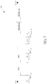
- FIG. 7 shows a charge pump circuit according to another embodiment of the present disclosure.
- FIG. 1 shows a charge pump unit 100 according to one embodiment of the present disclosure.
- the charge pump unit 100 includes an input terminal IN, an output terminal OUT, a first N-type transistor N 1 , a second N-type transistor N 2 , a first P-type transistor P 1 , a second P-type transistor P 2 , a first capacitor C 1 , a second capacitor C 2 , a clock input terminal CLK, P first inverters 110 , Q second inverters 120 , and R delay elements 130 .
- P is a positive integer
- Q is a non-negative integer smaller than P
- R is a positive integer.
- the first N-type transistor N 1 has a first terminal, a second terminal, a control terminal, and a body terminal.
- the first terminal of the first N-type transistor N 1 is coupled to the input terminal IN.
- the second N-type transistor N 2 has a first terminal, a second terminal, a control terminal, and a body terminal.
- the first terminal of the second N-type transistor N 2 is coupled to the input terminal IN
- the second terminal of the second N-type transistor N 2 is coupled to the control terminal of the first N-type transistor N 1
- the control terminal of the second N-type transistor N 2 is coupled to the second terminal of the first N-type transistor N 1 .
- the first P-type transistor P 1 has a first terminal, a second terminal, a control terminal, and a body terminal.
- the first terminal of the first P-type transistor P 1 is coupled to the second terminal of the first N-type transistor N 1
- the second terminal of the first P-type transistor P 1 is coupled to the output terminal OUT.
- the second P-type transistor P 2 has a first terminal, a second terminal, a control terminal, and a body terminal.
- the first terminal of the second P-type transistor P 2 is coupled to the second terminal of the second N-type transistor N 2 and the control terminal of the first P-type transistor P 1 , the second terminal of the second P-type transistor P 2 is coupled to the output terminal OUT, and the control terminal of the second P-type transistor P 2 is coupled to the first terminal of the first P-type transistor P 1 .
- the first capacitor C 1 has a first terminal and a second terminal. The first terminal of the first capacitor C 1 is coupled to the second terminal of the first N-type transistor N 1 .
- the second capacitor C 2 has a first terminal and a second terminal. The first terminal of the second capacitor C 2 is coupled to the second terminal of the second N-type transistor N 2 .
- the clock input terminal CLK receives a clock signal SIG CLK .
- the P first inverters 110 are coupled in series between the clock input terminal CLK and the second terminal of the first capacitor C 1 .
- the Q second inverters 120 and the R delay elements 130 are coupled in series between the clock input terminal CLK and the second terminal of the second capacitor C 2 .
- a difference between P and Q is an odd number so that the clock signal SIG CLKA received by the first capacitor C 1 and the clock signal SIG CLKB received by the second capacitor C 2 would be complementary to each other.
- P can be 3 and Q can be 2.
- the R delay elements 130 are coupled in series with the Q second inverters 120 between the clock input terminal CLK and the second terminal of the second capacitor C 2 .
- the R delay elements 130 can be designed to provide a proper delay so that the delay caused by the P first inverters 110 would be substantially equal to the delay caused by the Q second inverters 120 and the R delay elements 130 . Therefore, clock signal SIG CLKA and the clock signal SIG CLKB can toggle at the same time, reducing the reverse current of the charge pump unit 100 .
- FIG. 2 shows the waveforms of the clock signal SIG CLKA and the clock signal SIG CLKB .
- the clock signal SIG CLKA is at a first voltage VDD and the clock signal SIG CLKB is at a second voltage VSS lower than the first voltage VDD.
- the input terminal IN of the charge pump unit 100 may also receive the first voltage VDD.
- the first terminal of the first capacitor C 1 may have been charged to the first voltage VDD through the first N-type transistor N 1 while the second terminal of the first capacitor C 1 is at the second voltage VSS.
- the first terminal of the first capacitor C 1 is raised to a third voltage 2VDD, which is two times the first voltage VDD. Therefore, the second N-type transistor N 2 is turned on, so the first terminal of the second capacitor C 2 would be charged to the first voltage VDD through the second N-type transistor N 2 while the second terminal of the second capacitor C 2 would follow the clock signal SIG CLKB to be at the second voltage VSS.
- the first P-type transistor P 1 is turned on and the second P-type transistor P 2 is turned off. Therefore, the third voltage 2VDD would be outputted to the output terminal OUT through the first P-type transistor P 1 .
- the clock signal SIG CLKA is at the second voltage VSS and the clock signal SIG CLK2 is at the first voltage VDD. Since the first terminal of the second capacitor C 2 has been charged to the first voltage VDD through the second N-type transistor N 2 in period T 1 , the first terminal of the second capacitor C 2 would be raised to the third voltage 2VDD in period T 2 . Therefore, the first N-type transistor N 1 is turned on, so the first terminal of the first capacitor C 1 would be charged to the first voltage VDD while the second terminal of the first capacitor C 1 would follow the clock signal SIG CLKA to be at the second voltage VSS.
- the second P-type transistor P 2 is turned on and the first P-type transistor P 1 is turned off. Therefore, the third voltage 2VDD would be outputted to the output terminal OUT through the second P-type transistor P 2 .
- the first P-type transistor P 1 and the second P-type transistor P 2 can alternatively output the third voltage 2VDD, which is two times the input voltage VDD.
- the clock signal SIG CLKA and the clock signal SIG CLKB do not toggle at the same time, then the reverse current may occur. For example, if the clock signal SIG CLKB changes from the first voltage VDD to the second voltage VSS before the clock signal SIG CLKA changes from the second voltage VSS to the first voltage VDD, then the clock signal SIG CLKA and clock signal SIG CLKB would be both at the second voltage VSS in a short period.
- both the first P-type transistor P 1 and the second P-type transistor P 2 may be turned on, causing the reverse current to flow from the output terminal OUT back to the first terminal of the first P-type transistor P 1 and the first terminal of the second P-type transistor P 2 through the first P-type transistor P 1 and the second P-type transistor P 2 .
- the charge pump unit 100 can reduce the reverse current caused by the mismatched clock signals.
- FIG. 3 shows an inverter INV according to one embodiment of the present disclosure.
- the P first inverters 110 and the Q second inverters 120 each can have the same structure as the inverter INV.
- the inverter INV includes an input terminal, an output terminal, a P-type transistor INVP and an N-type transistor INVN.
- the P-type transistor INVP has a first terminal, a second terminal, and a control terminal.
- the first terminal of the P-type transistor INVP receives a first bias voltage, for example, the first voltage VDD
- the second terminal of the P-type transistor INVP is coupled to the output terminal of the inverter INV
- the control terminal of the P-type transistor INVP is coupled to the input terminal of the inverter INV.
- the N-type transistor INVN has a first terminal, a second terminal, and a control terminal.
- the first terminal of the N-type transistor INVN is coupled to the output terminal of the inverter INV
- the second terminal of the N-type transistor INVN receives the second bias voltage, for example, the second voltage VSS
- the control terminal of the N-type transistor INVN is coupled to the input terminal of the inverter INV.
- FIG. 4 shows a delay element DE according to one embodiment of the present disclosure.
- Each of the R delay elements 130 may have the same structure as the delay element DE.
- the delay element DE includes an input terminal, an output terminal, an N-type transistor DEN, and a P-type transistor DEP.
- the N-type transistor DEN has a first terminal, a second terminal, and a control terminal.
- the first terminal of the N-type transistor DEN is coupled to the input terminal of the delay element DE
- the second terminal of the N-type transistor DEN is coupled to the output terminal of the delay element DE
- the control terminal of the N-type transistor DEN receives the first bias voltage, for example, the first voltage VDD.
- the P-type transistor DEP has a first terminal, a second terminal, and a control terminal.
- the first terminal of the P-type transistor DEP is coupled to the input terminal of the delay element DE
- the second terminal of the P-type transistor DEP is coupled to the output terminal of the delay element DE
- the control terminal of the P-type transistor DEP receives the second bias voltage, for example the second voltage VSS.
- the delay element DE may be designed to have the channel width-to-length ratio of the N-type transistor DEN substantially equal to the channel width-to-length ratio of the N-type transistor INVN of the inverter INV. Also, the channel width-to-length ratio of the P-type transistor INVP of the inverter INV can be substantially equal to the channel width-to-length ratio of the P-type transistor DEP of the delay element DE.
- the P first inverters 110 and the Q second inverters 120 are implemented by the inverter INV and the R delay elements 130 are implemented by the delay element DE, then the sum of R and Q can be equal to P. Consequently, the delay caused by the P first inverters 110 would be equal to the delay caused by the Q second inverters 120 and the R delay elements 130 .
- P can be 3
- Q can be 2 and R can be 1.
- P can be 5, Q can be 2 and R can be 3.
- the charge pump unit 100 may use first inverters 110 and delay elements 130 without using the second inverters 120 .
- P can be 1, Q can be 0, and R can be 1.
- the first capacitor C 1 and the second capacitor C 2 can still receive the complementary clock signals with the same delay. Therefore, the reverse current can still be prevented.
- the delay caused by the delay element 130 can be different from the delay caused by the inverter 110 or 120 , and the number of P, Q, and R can be adjusted according to the system requirement.
- the charge pump unit 100 may further include a first initial pump transistor IT 1 and a second initial pump transistor IT 2 .
- the first initial pump transistor IT 1 has a first terminal, a second terminal, and a control terminal.
- the first terminal of the first initial pump transistor IT 1 is coupled to the input terminal IN of the charge pump unit 100
- the second terminal of the first initial pump transistor IT 1 is coupled to the second terminal of the first N-type transistor N 1
- the control terminal of the first initial pump transistor IT 1 is coupled to the input terminal IN of the charge pump unit 100 .
- the second initial pump transistor IT 2 has a first terminal, a second terminal, and a control terminal.
- the first terminal of the second initial pump transistor IT 2 is coupled to the input terminal IN of the charge pump unit 100
- the second terminal of the second initial pump transistor IT 2 is coupled to the second terminal of the second N-type transistor N 2
- the control terminal of the second initial pump transistor IT 2 is coupled to the input terminal IN of the charge pump unit 100 .
- the initial pump transistors IT 1 and IT 2 can be N-type transistors, and can be used to charge the second terminals of the first N-type transistor N 1 and the second N-type transistor N 2 to a voltage level equal to VDD-Vthn, Vthn is the threshold voltage of N-type transistors, in the beginning of the charge pump process, ensuring the charge pump unit 100 to become stable and output the pumped voltage faster.
- the charge pump unit 100 may further include a first pump precharge transistor TT 1 and a second pump precharge transistor TT 2 .
- the first pump precharge transistor TT 1 has a first terminal, a second terminal, and a control terminal.
- the first terminal of the first pump precharge transistor TT 1 is coupled to the second terminal of the first N-type transistor N 1
- the second terminal of the first pump precharge transistor TT 1 is coupled to the output terminal OUT of the charge pump unit 100
- the control terminal of the first pump precharge transistor TT 1 is coupled to the output terminal OUT of the charge pump unit 100 .
- the second pump precharge transistor TT 2 has a first terminal, a second terminal, and a control terminal.
- the first terminal of the second pump precharge transistor TT 2 is coupled to the second terminal of the second N-type transistor N 2 , the second terminal of the second pump precharge transistor TT 2 is coupled to the output terminal OUT of the charge pump unit 100 , and the control terminal of the second pump precharge transistor TT 2 is coupled to the output terminal OUT of the charge pump unit 100 .
- the pump precharge transistors TT 1 and TT 2 can be P-type transistors, and can be used to precharge the second terminals of the first P-type transistor P 1 and the second P-type transistor P 2 when the charge pump unit start pumping, reducing the output setting time of the charge pump unit 100 .
- the first pump precharge transistor TT 1 can be used to charge the second terminals of the first P-type transistor P 1 to a voltage level equal to 2VDD-Vthp, Vthp is the threshold voltage of P-type transistors, ensuring the charge pump unit 100 to become stable and output the pumped voltage faster.
- the charge pump unit 100 may further include a first well switch WS 1 .
- the first well switch WS 1 includes a third N-type transistor N 3 and a fourth N-type transistor N 4 .
- the third N-type transistor N 3 has a first terminal, a second terminal, a control terminal, and a body terminal.
- the first terminal of the third N-type transistor N 3 is coupled to the body terminal of the first N-type transistor N 1
- the second terminal of the third N-type transistor N 3 is coupled to the second terminal of the first N-type transistor N 1
- the control terminal of the third N-type transistor N 3 is coupled to first terminal of the first N-type transistor N 1
- the body terminal of the third N-type transistor N 3 is coupled to the body terminal of the first N-type transistor N 1 .
- the fourth N-type transistor N 4 has a first terminal, a second terminal, a control terminal, and a body terminal.
- the first terminal of the fourth N-type transistor N 4 is coupled to the first terminal of the first N-type transistor N 1
- the second terminal of the fourth N-type transistor N 4 is coupled to the body terminal of the first N-type transistor N 1
- the control terminal of the fourth N-type transistor N 4 is coupled to second terminal of the first N-type transistor N 1
- the body terminal of the fourth N-type transistor N 4 is coupled to the body terminal of the first N-type transistor N 1 .
- the voltage of the body terminal of the first N-type transistor N 1 can be controlled to be no greater than the voltages of the first terminal and the second terminals of the first N-type transistor N 1 . Therefore, the body effect and the leakage current caused on the body terminal of the first N-type transistor N 1 can be reduced.
- the charge pump unit 100 may further include a second well switch WS 2 , a third well switch WS 3 and a fourth well switch WS 4 for avoiding the leakage currents caused on the body terminals of the second N-type transistor N 2 , the first P-type transistor P 1 , and the second P-type transistor P 2 respectively.
- the second to fourth well switches WS 2 to WS 4 may have the similar structure as the well switch WS 1 . That is, the second well switch WS 2 may include a fifth N-type transistor N 5 and a sixth N-type transistor N 6 . The fifth N-type transistor N 5 and the sixth N-type transistor N 6 may be coupled to the second N-type transistor N 2 in the same manner as the third N-type transistor N 3 and the fourth N-type transistor N 4 coupling to the first N-type transistor N 1 .
- the third well switch WS 3 may include a third P-type transistor P 3 and a fourth P-type transistor P 4 .
- the third P-type transistor P 3 and the fourth P-type transistor P 4 may be coupled to the first P-type transistor P 1 in the same manner as the third N-type transistor N 3 and the fourth N-type transistor N 4 coupling to the first N-type transistor N 1 .
- the fourth well switch WS 4 may include a fifth P-type transistor P 5 and a sixth P-type transistor P 6 .
- the fifth P-type transistor P 5 and the sixth P-type transistor P 6 may be coupled to the second P-type transistor P 2 in the same manner as the third N-type transistor N 3 and the fourth N-type transistor N 4 coupling to the first N-type transistor N 1 .
- FIG. 5 shows a charge pump circuit 10 according to one embodiment of the present disclosure.
- the charge pump circuit 10 includes a voltage input port VIN, a voltage output port VOUT, (N+1) charge pump units 1001 to 100 (N+1), a clock signal source 12 , and N clock delay elements 141 to 14 N.
- N is a positive integer.
- the (N+1) charge pump units 1001 to 100 (N+1) are cascaded between the voltage input port VIN and the voltage output port VOUT.
- a first charge pump unit 1001 of the (N+1) charge pump units 1001 to 100 (N+1) is coupled to the voltage input port VIN
- a last charge pump unit 100 (N+1) of the (N+1) charge pump units 1001 to 100 (N+1) is coupled to the voltage output port VOUT.
- each of the charge pump units 1001 to 100 (N+1) may have the same structure as the charge pump unit 100 as shown in FIG. 1 . Therefore, with the voltage input port VIN receiving the first voltage VDD, the voltage output port VOUT can output a voltage that is (N+2) times the first voltage VDD, that is (N+2)VDD.
- the charge pump units 1001 to 100 (N+1) are able to produce two synchronized complementary clock signals themselves according to the single clock signal received.
- the charge pump units 1001 to 100 (N+1) when receiving the main clock signal SIG CLK1 generated by the clock signal source 12 , the charge pump units 1001 to 100 (N+1) can produce the two complementary clock signals accordingly. However, if the complementary clocks generated by the charge pump units 1001 to 100 (N+1) are toggling simultaneously, then the capacitors of the charge pump units 1001 to 100 (N+1) would be charged at the same time, causing high peak current each time when the two complementary clock signals toggle. Therefore, in FIG. 5 , the N clock delay elements 141 to 14 N are cascaded and coupled to the clock signal source 12 for generating the clock signals required by the charge pump units 1002 to 100 (N+1) by delaying the main clock signal SIG CLK1 . Also, each of the clock delay elements 141 to 14 N can produce a clock signal by delaying the received clock signal with a predetermined period.
- the output terminal of the first clock delay element 141 is coupled to the clock input terminal CLK of the second charge pump unit 1002
- the output terminal of the second clock delay element 142 is coupled to the clock input terminal CLK of the third charge pump unit 1003 .
- the clock signal SIG CLK2 is outputted to the second clock delay element 142 for generating the clock signal SIG CLK3 Therefore, the clock signal SIG CLK3 would be further delayed according to the clock signal SIG CLK2 .
- FIG. 6 shows the waveforms of the main clock signal SIG CLK1 generated by the clock signal source 12 and the clock signals SIG CLK2 to SIG CLK (N+1) generated by the clock delay elements 141 to 14 N.
- the main clock signal SIG CLK1 and the clock signals SIG CLK2 to SIG CL(N+1) are toggled sequentially.
- the main clock signal SIG CLK1 has a rising edge RE 1 leading the rising edge RE 2 of the clock signal SIG CLK2 , and the rising edge RE 2 leads the rising edge RE 3 of the clock signal SIG CLK3 .
- the rising edge REi of the clock signal SIG CLK1 leads the rising edge RE (i+1) of the clock signal SIG CLK(i+1) , wherein i is an integer greater than 1 and smaller than N+1.
- the main clock signal SIG CLK1 has a falling edge FE 1 lagging the rising edge RE (N+1) of the second clock signal SIG CLK(N+1) .
- the falling edge FE 1 leads the falling edge FE 2 of the clock signal SIG CLK2
- the falling edge FEi of the clock signal SIG CLKi leads the falling edge FE (i+1) of the clock signal SIG CLK(i+1) . That is, the clock signals SIG CLK2 to SIG CLK(N+1) can be seen as a sequential of clock signals generated by shifting the main clock signal SIG CLK1 .
- the first charge pump unit 1001 receiving the main clock signal SIG CLK1 would be charged first
- the second charge pump unit 1002 receiving the clock signal SIG CLK2 would be charged second
- the charge pump units 1001 to 100 (N+1) will not be charged at the same time, and the high peak current induced in the prior art can be avoided.
- FIG. 5 shows a charge pump circuit 20 according to another embodiment of the present disclosure.
- the structure of charge pump circuit 20 is similar to the structure of the charge pump circuit 10 .
- the charge pump circuit 20 includes (2N+2) charge pump units 1001 to 100 (2N+2).
- each pair of charge pump units would receive the same clock signal.
- the charge pump units 1001 and 1002 would receive the main clock signal SIG CLK1
- the charge pump units 100 (2N+1) and 100 (2N+2) would receive the clock signal SIG CLK(N+1) . Therefore, as the number of charge pump units increases, the number of the clock delay elements will increase in a slower rate, reducing the burden for meeting the area requirement of the charge pump circuit.
- the more charge pump units receive the same clock signal the higher peak current the charge pump circuit may produce. Therefore, the charge pump circuit can be designed to have different number of charge pump units receiving the same clock signal according to the system requirement.
- the charge pump units and the charge pump circuits provided by the embodiments of the present disclosure can use the delay elements and inverters to generate complementary clock signals accurately, reducing the reverse current and simplifying the clock control of the charge pump circuits. Furthermore, by delaying the clock signal of each stage of charge pump unit in the charge pump circuit, the peak current can also be reduced significantly.
Abstract
Description
Claims (7)
Priority Applications (1)
| Application Number | Priority Date | Filing Date | Title |
|---|---|---|---|
| US16/247,584 US10714155B2 (en) | 2016-05-25 | 2019-01-15 | Charge pump circuit with low reverse current and low peak current |
Applications Claiming Priority (3)
| Application Number | Priority Date | Filing Date | Title |
|---|---|---|---|
| US201662341105P | 2016-05-25 | 2016-05-25 | |
| US15/604,662 US10224079B2 (en) | 2016-05-25 | 2017-05-25 | Charge pump circuit with low reverse current and low peak current |
| US16/247,584 US10714155B2 (en) | 2016-05-25 | 2019-01-15 | Charge pump circuit with low reverse current and low peak current |
Related Parent Applications (1)
| Application Number | Title | Priority Date | Filing Date |
|---|---|---|---|
| US15/604,662 Division US10224079B2 (en) | 2016-05-25 | 2017-05-25 | Charge pump circuit with low reverse current and low peak current |
Publications (2)
| Publication Number | Publication Date |
|---|---|
| US20190147922A1 US20190147922A1 (en) | 2019-05-16 |
| US10714155B2 true US10714155B2 (en) | 2020-07-14 |
Family
ID=60418184
Family Applications (5)
| Application Number | Title | Priority Date | Filing Date |
|---|---|---|---|
| US15/603,478 Active US10090027B2 (en) | 2016-05-25 | 2017-05-24 | Memory system with low read power |
| US15/604,664 Active US10003258B2 (en) | 2016-05-25 | 2017-05-25 | Charge pump circuit with a low reverse current |
| US15/604,672 Active US9935113B2 (en) | 2016-05-25 | 2017-05-25 | Non-volatile memory and method for programming and reading a memory array having the same |
| US15/604,662 Active US10224079B2 (en) | 2016-05-25 | 2017-05-25 | Charge pump circuit with low reverse current and low peak current |
| US16/247,584 Active US10714155B2 (en) | 2016-05-25 | 2019-01-15 | Charge pump circuit with low reverse current and low peak current |
Family Applications Before (4)
| Application Number | Title | Priority Date | Filing Date |
|---|---|---|---|
| US15/603,478 Active US10090027B2 (en) | 2016-05-25 | 2017-05-24 | Memory system with low read power |
| US15/604,664 Active US10003258B2 (en) | 2016-05-25 | 2017-05-25 | Charge pump circuit with a low reverse current |
| US15/604,672 Active US9935113B2 (en) | 2016-05-25 | 2017-05-25 | Non-volatile memory and method for programming and reading a memory array having the same |
| US15/604,662 Active US10224079B2 (en) | 2016-05-25 | 2017-05-25 | Charge pump circuit with low reverse current and low peak current |
Country Status (5)
| Country | Link |
|---|---|
| US (5) | US10090027B2 (en) |
| EP (1) | EP3407355B1 (en) |
| JP (2) | JP6389925B1 (en) |
| CN (4) | CN108964444B (en) |
| TW (4) | TWI666865B (en) |
Families Citing this family (32)
| Publication number | Priority date | Publication date | Assignee | Title |
|---|---|---|---|---|
| US11625523B2 (en) | 2016-12-14 | 2023-04-11 | iCometrue Company Ltd. | Logic drive based on standard commodity FPGA IC chips |
| TWI824467B (en) | 2016-12-14 | 2023-12-01 | 成真股份有限公司 | Logic drive based on standard commodity fpga ic chips |
| US10447274B2 (en) | 2017-07-11 | 2019-10-15 | iCometrue Company Ltd. | Logic drive based on standard commodity FPGA IC chips using non-volatile memory cells |
| US10957679B2 (en) | 2017-08-08 | 2021-03-23 | iCometrue Company Ltd. | Logic drive based on standardized commodity programmable logic semiconductor IC chips |
| US10630296B2 (en) | 2017-09-12 | 2020-04-21 | iCometrue Company Ltd. | Logic drive with brain-like elasticity and integrality based on standard commodity FPGA IC chips using non-volatile memory cells |
| US10608642B2 (en) | 2018-02-01 | 2020-03-31 | iCometrue Company Ltd. | Logic drive using standard commodity programmable logic IC chips comprising non-volatile radom access memory cells |
| US10623000B2 (en) | 2018-02-14 | 2020-04-14 | iCometrue Company Ltd. | Logic drive using standard commodity programmable logic IC chips |
| US10608638B2 (en) | 2018-05-24 | 2020-03-31 | iCometrue Company Ltd. | Logic drive using standard commodity programmable logic IC chips |
| KR102577262B1 (en) | 2018-08-14 | 2023-09-11 | 삼성전자주식회사 | Semiconductor device including diffusion break region |
| US11309334B2 (en) | 2018-09-11 | 2022-04-19 | iCometrue Company Ltd. | Logic drive using standard commodity programmable logic IC chips comprising non-volatile random access memory cells |
| US10892011B2 (en) | 2018-09-11 | 2021-01-12 | iCometrue Company Ltd. | Logic drive using standard commodity programmable logic IC chips comprising non-volatile random access memory cells |
| US10937762B2 (en) | 2018-10-04 | 2021-03-02 | iCometrue Company Ltd. | Logic drive based on multichip package using interconnection bridge |
| US11616046B2 (en) | 2018-11-02 | 2023-03-28 | iCometrue Company Ltd. | Logic drive based on chip scale package comprising standardized commodity programmable logic IC chip and memory IC chip |
| US11056197B2 (en) | 2018-11-08 | 2021-07-06 | Samsung Electronics Co., Ltd. | Charge pump and memory device including the same |
| KR20200053324A (en) * | 2018-11-08 | 2020-05-18 | 삼성전자주식회사 | Charge pump and memory device having charge pump |
| TWI708253B (en) | 2018-11-16 | 2020-10-21 | 力旺電子股份有限公司 | Nonvolatile memory yield improvement and testing method |
| US11211334B2 (en) | 2018-11-18 | 2021-12-28 | iCometrue Company Ltd. | Logic drive based on chip scale package comprising standardized commodity programmable logic IC chip and memory IC chip |
| US11360704B2 (en) | 2018-12-21 | 2022-06-14 | Micron Technology, Inc. | Multiplexed signal development in a memory device |
| US10818592B1 (en) * | 2019-04-29 | 2020-10-27 | Nanya Technology Corporation | Semiconductor memory device including decoupling capacitor array arranged overlying one-time programmable device |
| US11227838B2 (en) | 2019-07-02 | 2022-01-18 | iCometrue Company Ltd. | Logic drive based on multichip package comprising standard commodity FPGA IC chip with cooperating or supporting circuits |
| US10985154B2 (en) | 2019-07-02 | 2021-04-20 | iCometrue Company Ltd. | Logic drive based on multichip package comprising standard commodity FPGA IC chip with cryptography circuits |
| CN110299173B (en) * | 2019-07-05 | 2021-05-04 | 合肥联诺科技股份有限公司 | Controllable discharging module for NOR FLASH programming processing |
| US11404415B2 (en) * | 2019-07-05 | 2022-08-02 | Globalfoundries U.S. Inc. | Stacked-gate transistors |
| US11887930B2 (en) | 2019-08-05 | 2024-01-30 | iCometrue Company Ltd. | Vertical interconnect elevator based on through silicon vias |
| US11637056B2 (en) | 2019-09-20 | 2023-04-25 | iCometrue Company Ltd. | 3D chip package based on through-silicon-via interconnection elevator |
| US10957701B1 (en) * | 2019-11-11 | 2021-03-23 | Globalfoundries U.S. Inc. | Fin-based anti-fuse device for integrated circuit (IC) products, methods of making such an anti-fuse device and IC products comprising such an anti-fuse device |
| US11600526B2 (en) | 2020-01-22 | 2023-03-07 | iCometrue Company Ltd. | Chip package based on through-silicon-via connector and silicon interconnection bridge |
| US11328957B2 (en) * | 2020-02-25 | 2022-05-10 | Taiwan Semiconductor Manufacturing Co., Ltd. | Semiconductor device and manufacturing method thereof |
| US11270780B2 (en) | 2020-03-31 | 2022-03-08 | Taiwan Semiconductor Manufacturing Co., Ltd. | Memory readout circuit and method |
| US11183502B1 (en) * | 2020-08-20 | 2021-11-23 | Nanya Technology Corporation | Memory cell and Method for reading out data therefrom |
| CN112039335A (en) * | 2020-08-21 | 2020-12-04 | 厦门半导体工业技术研发有限公司 | Voltage generator and semiconductor device |
| CN116137493A (en) | 2021-11-17 | 2023-05-19 | 科奇芯有限公司 | Charge pump circuit |
Citations (11)
| Publication number | Priority date | Publication date | Assignee | Title |
|---|---|---|---|---|
| US5687128A (en) * | 1994-12-20 | 1997-11-11 | Samsung Electronics Co., Ltd. | Power supply voltage boosting circuit of semiconductor memory device |
| US5874850A (en) | 1994-08-12 | 1999-02-23 | Stmicroelectronics S.R.L. | Mos voltage elevator of the charge pump type |
| US6483377B2 (en) | 2001-01-10 | 2002-11-19 | Texas Instruments Incorporated | Low slew rate charge pump |
| US20030122611A1 (en) | 2001-12-29 | 2003-07-03 | Hynix Semiconductor Inc. | Charge pump circuit |
| CN1835365A (en) | 2005-03-16 | 2006-09-20 | 三菱电机株式会社 | Frequency dividing circuit, power supply circuit and display device |
| CN101056104A (en) | 2006-04-12 | 2007-10-17 | 国际商业机器公司 | Delay locked loop having charge pump gain independent of operating frequency |
| TW200840211A (en) | 2007-03-20 | 2008-10-01 | Novatek Microelectronics Corp | Charge pump circuit |
| US7439795B2 (en) | 2006-11-14 | 2008-10-21 | Nec Electronics Corporation | Charge pump circuit with reduced parasitic capacitance |
| CN101409554A (en) | 2007-10-11 | 2009-04-15 | 北京朗波芯微技术有限公司 | Loop filter circuit for charge pump phase-locked loop |
| TW201023488A (en) | 2008-12-02 | 2010-06-16 | Himax Tech Ltd | Charge pump circuit and method thereof |
| TWI574498B (en) | 2015-01-07 | 2017-03-11 | 力旺電子股份有限公司 | Charge pump unit and charge pump circuit |
Family Cites Families (60)
| Publication number | Priority date | Publication date | Assignee | Title |
|---|---|---|---|---|
| JP2537264B2 (en) | 1988-04-13 | 1996-09-25 | 株式会社東芝 | Semiconductor memory device |
| JP3076606B2 (en) | 1990-12-14 | 2000-08-14 | 富士通株式会社 | Semiconductor memory device and inspection method thereof |
| US5126590A (en) * | 1991-06-17 | 1992-06-30 | Micron Technology, Inc. | High efficiency charge pump |
| JP3178946B2 (en) | 1993-08-31 | 2001-06-25 | 沖電気工業株式会社 | Semiconductor memory device and driving method thereof |
| JPH0778465A (en) | 1993-09-10 | 1995-03-20 | Oki Micro Design Miyazaki:Kk | Semiconductor integrated circuit |
| KR0149220B1 (en) | 1994-12-27 | 1998-12-01 | 김주용 | Charge pump circuit |
| US5729493A (en) | 1996-08-23 | 1998-03-17 | Motorola Inc. | Memory suitable for operation at low power supply voltages and sense amplifier therefor |
| JP3378457B2 (en) * | 1997-02-26 | 2003-02-17 | 株式会社東芝 | Semiconductor device |
| JP3557090B2 (en) | 1998-03-31 | 2004-08-25 | 株式会社東芝 | Semiconductor storage device |
| US6501325B1 (en) * | 2001-01-18 | 2002-12-31 | Cypress Semiconductor Corp. | Low voltage supply higher efficiency cross-coupled high voltage charge pumps |
| US6661682B2 (en) * | 2001-02-16 | 2003-12-09 | Imec (Interuniversitair Microelectronica Centrum) | High voltage generating charge pump circuit |
| JP2003077282A (en) | 2001-08-31 | 2003-03-14 | Fujitsu Ltd | Nonvolatile semiconductor memory |
| KR100454144B1 (en) * | 2001-11-23 | 2004-10-26 | 주식회사 하이닉스반도체 | Flash memory device having a multi bank structure |
| KR100538883B1 (en) * | 2003-04-29 | 2005-12-23 | 주식회사 하이닉스반도체 | Semiconductor memory apparatus |
| CN1455574A (en) * | 2003-05-30 | 2003-11-12 | 无敌科技(西安)有限公司 | Selective information storage system and its realizing method |
| US7411840B2 (en) * | 2004-03-02 | 2008-08-12 | Via Technologies, Inc. | Sense mechanism for microprocessor bus inversion |
| US6995603B2 (en) * | 2004-03-03 | 2006-02-07 | Aimtron Technology Corp. | High efficiency charge pump with prevention from reverse current |
| US7551503B2 (en) * | 2005-06-24 | 2009-06-23 | Macronix International Co., Ltd. | Method for refreshing a flash memory |
| JP4728726B2 (en) * | 2005-07-25 | 2011-07-20 | 株式会社東芝 | Semiconductor memory device |
| JP2007034943A (en) * | 2005-07-29 | 2007-02-08 | Sony Corp | Shared memory device |
| CN101154683B (en) * | 2006-09-29 | 2011-03-30 | 旺宏电子股份有限公司 | Transistor structure and its manufacturing method |
| KR20080029696A (en) * | 2006-09-29 | 2008-04-03 | 주식회사 하이닉스반도체 | Redundancy circuit for seminconductor memory device |
| KR100818710B1 (en) * | 2006-11-21 | 2008-04-01 | 주식회사 하이닉스반도체 | Voltage pumping device |
| JP4498374B2 (en) * | 2007-03-22 | 2010-07-07 | 株式会社東芝 | Semiconductor memory device |
| US7656731B2 (en) * | 2007-03-30 | 2010-02-02 | Qualcomm, Incorporated | Semi-shared sense amplifier and global read line architecture |
| US7446596B1 (en) | 2007-05-25 | 2008-11-04 | Atmel Corporation | Low voltage charge pump |
| KR101102776B1 (en) | 2008-02-13 | 2012-01-05 | 매그나칩 반도체 유한회사 | Unit cell of nonvolatile memory device and nonvolatile memory device having the same |
| US7859043B2 (en) * | 2008-02-25 | 2010-12-28 | Tower Semiconductor Ltd. | Three-terminal single poly NMOS non-volatile memory cell |
| CN101685677A (en) * | 2008-09-27 | 2010-03-31 | 英华达(上海)科技有限公司 | Flash memory detector and method thereof |
| US8144537B2 (en) | 2008-11-11 | 2012-03-27 | Stmicroelectronics Pvt. Ltd. | Balanced sense amplifier for single ended bitline memory architecture |
| US8154936B2 (en) * | 2008-12-30 | 2012-04-10 | Stmicroelectronics Pvt. Ltd. | Single-ended bit line based storage system |
| US8305790B2 (en) | 2009-03-16 | 2012-11-06 | Taiwan Semiconductor Manufacturing Company, Ltd. | Electrical anti-fuse and related applications |
| US9042173B2 (en) | 2010-01-29 | 2015-05-26 | Texas Instruments Incorporated | Efficient memory sense architecture |
| TW201203253A (en) | 2010-07-06 | 2012-01-16 | Maxchip Electronics Corp | One time programmable memory and the manufacturing method and operation method thereof |
| JP5673935B2 (en) * | 2010-12-28 | 2015-02-18 | セイコーエプソン株式会社 | Nonvolatile storage device, electronic device |
| CN102646387B (en) * | 2011-05-19 | 2014-09-17 | 京东方科技集团股份有限公司 | Shift register and line-scanning driving circuit |
| KR20130093303A (en) * | 2012-02-14 | 2013-08-22 | 에스케이하이닉스 주식회사 | Charge pumping device and unit cell thereof |
| FR2988535B1 (en) * | 2012-03-23 | 2014-03-07 | Soitec Silicon On Insulator | TRANSISTOR LOAD PUMP CIRCUIT WITH DOUBLE PHASE DOORS AND METHOD OF OPERATING SAID CIRCUIT. |
| JP5444414B2 (en) | 2012-06-04 | 2014-03-19 | 株式会社東芝 | Magnetic random access memory |
| CN103456711B (en) * | 2012-06-05 | 2016-03-23 | 中芯国际集成电路制造(上海)有限公司 | Fin-type anti-fuse structure and manufacture method thereof |
| US9070424B2 (en) | 2012-06-29 | 2015-06-30 | Samsung Electronics Co., Ltd. | Sense amplifier circuitry for resistive type memory |
| US9536883B2 (en) * | 2012-07-12 | 2017-01-03 | Broadcom Corporation | Dual anti-fuse |
| US9337318B2 (en) * | 2012-10-26 | 2016-05-10 | Taiwan Semiconductor Manufacturing Company, Ltd. | FinFET with dummy gate on non-recessed shallow trench isolation (STI) |
| US9601499B2 (en) * | 2013-05-16 | 2017-03-21 | Ememory Technology Inc. | One-time programmable memory cell capable of reducing leakage current and preventing slow bit response, and method for programming a memory array comprising the same |
| TWI502722B (en) | 2013-07-24 | 2015-10-01 | Ememory Technology Inc | Antifuse otp memory cell with performance improvement and operating method of memory |
| US20150078103A1 (en) * | 2013-09-13 | 2015-03-19 | Lsi Corporation | Sensing technique for single-ended bit line memory architectures |
| US20150194433A1 (en) * | 2014-01-08 | 2015-07-09 | Broadcom Corporation | Gate substantial contact based one-time programmable device |
| CN104979362B (en) * | 2014-04-10 | 2019-11-19 | 三星电子株式会社 | Semiconductor device with finned active patterns and gate node |
| US9171752B1 (en) | 2014-08-12 | 2015-10-27 | Globalfoundries Inc. | Product comprised of FinFET devices with single diffusion break isolation structures, and methods of making such a product |
| US9460761B2 (en) * | 2014-08-14 | 2016-10-04 | Stmicroelectronics (Rousset) Sas | Lower power sense amplifier for reading non-volatile memory cells |
| KR102179169B1 (en) * | 2014-09-02 | 2020-11-18 | 삼성전자주식회사 | Semiconductor device and method for manufacturing semiconductor device |
| DE102014115433A1 (en) * | 2014-10-23 | 2016-05-12 | Infineon Technologies Ag | charge pump |
| US9620176B2 (en) | 2015-09-10 | 2017-04-11 | Ememory Technology Inc. | One-time programmable memory array having small chip area |
| US10109364B2 (en) | 2015-10-21 | 2018-10-23 | Avago Technologies General Ip (Singapore) Pte. Ltd. | Non-volatile memory cell having multiple signal pathways to provide access to an antifuse of the memory cell |
| US9613714B1 (en) * | 2016-01-19 | 2017-04-04 | Ememory Technology Inc. | One time programming memory cell and memory array for physically unclonable function technology and associated random code generating method |
| JP6200983B2 (en) * | 2016-01-25 | 2017-09-20 | 力旺電子股▲ふん▼有限公司eMemory Technology Inc. | One-time programmable memory cell, method for programming and reading memory array including the memory cell |
| US9536991B1 (en) | 2016-03-11 | 2017-01-03 | Globalfoundries Inc. | Single diffusion break structure |
| CN107306082B (en) * | 2016-04-18 | 2020-05-22 | 晶门科技(深圳)有限公司 | Charge pump circuit |
| CN205883044U (en) * | 2016-07-06 | 2017-01-11 | 西安紫光国芯半导体有限公司 | Charge pump circuit and single -level circuit thereof |
| US9589970B1 (en) | 2016-08-02 | 2017-03-07 | United Microelectronics Corp. | Antifuse one-time programmable memory |
-
2017
- 2017-05-24 US US15/603,478 patent/US10090027B2/en active Active
- 2017-05-25 US US15/604,664 patent/US10003258B2/en active Active
- 2017-05-25 US US15/604,672 patent/US9935113B2/en active Active
- 2017-05-25 US US15/604,662 patent/US10224079B2/en active Active
- 2017-06-02 JP JP2017109618A patent/JP6389925B1/en active Active
- 2017-06-08 JP JP2017113074A patent/JP2018201002A/en active Pending
- 2017-06-26 EP EP17177772.5A patent/EP3407355B1/en active Active
- 2017-07-27 TW TW106125243A patent/TWI666865B/en active
- 2017-08-11 CN CN201710687034.6A patent/CN108964444B/en active Active
- 2017-08-17 TW TW106127886A patent/TWI636652B/en active
- 2017-08-23 CN CN201710729296.4A patent/CN108964446B/en active Active
- 2017-09-28 TW TW106133409A patent/TWI630708B/en active
- 2017-10-06 TW TW106134435A patent/TWI630621B/en active
- 2017-10-10 CN CN201710932265.9A patent/CN108932965B/en active Active
- 2017-10-18 CN CN201710972339.1A patent/CN108962332B/en active Active
-
2019
- 2019-01-15 US US16/247,584 patent/US10714155B2/en active Active
Patent Citations (14)
| Publication number | Priority date | Publication date | Assignee | Title |
|---|---|---|---|---|
| US5874850A (en) | 1994-08-12 | 1999-02-23 | Stmicroelectronics S.R.L. | Mos voltage elevator of the charge pump type |
| US5687128A (en) * | 1994-12-20 | 1997-11-11 | Samsung Electronics Co., Ltd. | Power supply voltage boosting circuit of semiconductor memory device |
| US6483377B2 (en) | 2001-01-10 | 2002-11-19 | Texas Instruments Incorporated | Low slew rate charge pump |
| US20030122611A1 (en) | 2001-12-29 | 2003-07-03 | Hynix Semiconductor Inc. | Charge pump circuit |
| US6734717B2 (en) * | 2001-12-29 | 2004-05-11 | Hynix Semiconductor Inc. | Charge pump circuit |
| US7504869B2 (en) | 2005-03-16 | 2009-03-17 | Mitsubishi Denki Kabushiki Kaisha | Frequency dividing circuit, power supply circuit and display device |
| CN1835365A (en) | 2005-03-16 | 2006-09-20 | 三菱电机株式会社 | Frequency dividing circuit, power supply circuit and display device |
| CN101056104A (en) | 2006-04-12 | 2007-10-17 | 国际商业机器公司 | Delay locked loop having charge pump gain independent of operating frequency |
| US20070241798A1 (en) | 2006-04-12 | 2007-10-18 | Masenas Charles J | Delay locked loop having charge pump gain independent of operating frequency |
| US7439795B2 (en) | 2006-11-14 | 2008-10-21 | Nec Electronics Corporation | Charge pump circuit with reduced parasitic capacitance |
| TW200840211A (en) | 2007-03-20 | 2008-10-01 | Novatek Microelectronics Corp | Charge pump circuit |
| CN101409554A (en) | 2007-10-11 | 2009-04-15 | 北京朗波芯微技术有限公司 | Loop filter circuit for charge pump phase-locked loop |
| TW201023488A (en) | 2008-12-02 | 2010-06-16 | Himax Tech Ltd | Charge pump circuit and method thereof |
| TWI574498B (en) | 2015-01-07 | 2017-03-11 | 力旺電子股份有限公司 | Charge pump unit and charge pump circuit |
Also Published As
| Publication number | Publication date |
|---|---|
| CN108964446B (en) | 2020-08-25 |
| JP2018198105A (en) | 2018-12-13 |
| TWI630621B (en) | 2018-07-21 |
| US10090027B2 (en) | 2018-10-02 |
| US20170346394A1 (en) | 2017-11-30 |
| US20170346393A1 (en) | 2017-11-30 |
| TWI630708B (en) | 2018-07-21 |
| TW201901929A (en) | 2019-01-01 |
| CN108962332A (en) | 2018-12-07 |
| US10003258B2 (en) | 2018-06-19 |
| TW201902097A (en) | 2019-01-01 |
| JP2018201002A (en) | 2018-12-20 |
| EP3407355B1 (en) | 2020-04-29 |
| TWI666865B (en) | 2019-07-21 |
| CN108932965B (en) | 2020-12-01 |
| TW201901674A (en) | 2019-01-01 |
| CN108964446A (en) | 2018-12-07 |
| US20170345828A1 (en) | 2017-11-30 |
| CN108932965A (en) | 2018-12-04 |
| TWI636652B (en) | 2018-09-21 |
| JP6389925B1 (en) | 2018-09-12 |
| TW201902096A (en) | 2019-01-01 |
| US10224079B2 (en) | 2019-03-05 |
| EP3407355A1 (en) | 2018-11-28 |
| US9935113B2 (en) | 2018-04-03 |
| CN108964444B (en) | 2020-05-29 |
| US20170345464A1 (en) | 2017-11-30 |
| US20190147922A1 (en) | 2019-05-16 |
| CN108962332B (en) | 2021-03-23 |
| CN108964444A (en) | 2018-12-07 |
Similar Documents
| Publication | Publication Date | Title |
|---|---|---|
| US10714155B2 (en) | Charge pump circuit with low reverse current and low peak current | |
| US9385596B1 (en) | Charge pump circuit capable of reducing reverse currents | |
| US7902909B2 (en) | Charge pump circuit | |
| JP2009509449A (en) | Single threshold, single conductivity type logic circuit | |
| TWI392209B (en) | Charge pump circuit and method thereof | |
| US9360881B2 (en) | Drive circuit, integrated circuit device, and method for controlling charge pump circuit | |
| CN112769319B (en) | Level conversion module, drive circuit and control chip | |
| US7924086B2 (en) | Boosting circuit | |
| US10483954B2 (en) | Clock generation circuit and charge pumping system | |
| CN108696118B (en) | Boosting circuit and method for biasing substrate therein | |
| TWI602386B (en) | Charge pump circuit | |
| US10236876B2 (en) | Switch control circuit with booster | |
| CN105336368B (en) | Non-overlapping four-phase clock generation circuit | |
| US20200244162A1 (en) | Charge pump circuit, semiconductor device, and semiconductor memory device | |
| JP6637695B2 (en) | Charge pump circuit | |
| CN108233702B (en) | Charge pump circuit | |
| JP4581415B2 (en) | Pulse booster circuit, booster circuit, and charge pump circuit | |
| CN115694178A (en) | Charge pump circuit and charge pump system |
Legal Events
| Date | Code | Title | Description |
|---|---|---|---|
| FEPP | Fee payment procedure |
Free format text: ENTITY STATUS SET TO UNDISCOUNTED (ORIGINAL EVENT CODE: BIG.); ENTITY STATUS OF PATENT OWNER: SMALL ENTITY |
|
| FEPP | Fee payment procedure |
Free format text: ENTITY STATUS SET TO SMALL (ORIGINAL EVENT CODE: SMAL); ENTITY STATUS OF PATENT OWNER: SMALL ENTITY |
|
| STPP | Information on status: patent application and granting procedure in general |
Free format text: DOCKETED NEW CASE - READY FOR EXAMINATION |
|
| STPP | Information on status: patent application and granting procedure in general |
Free format text: NON FINAL ACTION MAILED |
|
| STPP | Information on status: patent application and granting procedure in general |
Free format text: RESPONSE TO NON-FINAL OFFICE ACTION ENTERED AND FORWARDED TO EXAMINER |
|
| STPP | Information on status: patent application and granting procedure in general |
Free format text: NOTICE OF ALLOWANCE MAILED -- APPLICATION RECEIVED IN OFFICE OF PUBLICATIONS |
|
| STPP | Information on status: patent application and granting procedure in general |
Free format text: PUBLICATIONS -- ISSUE FEE PAYMENT VERIFIED |
|
| STCF | Information on status: patent grant |
Free format text: PATENTED CASE |
|
| MAFP | Maintenance fee payment |
Free format text: PAYMENT OF MAINTENANCE FEE, 4TH YR, SMALL ENTITY (ORIGINAL EVENT CODE: M2551); ENTITY STATUS OF PATENT OWNER: SMALL ENTITY Year of fee payment: 4 |