US10700161B2 - Substrate structure and manufacturing method thereof - Google Patents
Substrate structure and manufacturing method thereof Download PDFInfo
- Publication number
- US10700161B2 US10700161B2 US16/159,726 US201816159726A US10700161B2 US 10700161 B2 US10700161 B2 US 10700161B2 US 201816159726 A US201816159726 A US 201816159726A US 10700161 B2 US10700161 B2 US 10700161B2
- Authority
- US
- United States
- Prior art keywords
- dielectric layer
- layer
- build
- circuit
- circuit structure
- Prior art date
- Legal status (The legal status is an assumption and is not a legal conclusion. Google has not performed a legal analysis and makes no representation as to the accuracy of the status listed.)
- Active
Links
- 239000000758 substrate Substances 0.000 title claims abstract description 66
- 238000004519 manufacturing process Methods 0.000 title abstract description 27
- RYGMFSIKBFXOCR-UHFFFAOYSA-N Copper Chemical compound [Cu] RYGMFSIKBFXOCR-UHFFFAOYSA-N 0.000 claims abstract description 40
- 239000010949 copper Substances 0.000 claims abstract description 40
- 229910052802 copper Inorganic materials 0.000 claims abstract description 40
- 239000010410 layer Substances 0.000 claims description 254
- 239000011521 glass Substances 0.000 claims description 23
- 229910000679 solder Inorganic materials 0.000 claims description 12
- 239000012790 adhesive layer Substances 0.000 claims description 7
- 230000001939 inductive effect Effects 0.000 claims description 7
- 230000000149 penetrating effect Effects 0.000 claims 2
- 238000000034 method Methods 0.000 description 14
- 239000000463 material Substances 0.000 description 11
- 239000003990 capacitor Substances 0.000 description 7
- RTAQQCXQSZGOHL-UHFFFAOYSA-N Titanium Chemical compound [Ti] RTAQQCXQSZGOHL-UHFFFAOYSA-N 0.000 description 6
- 239000010936 titanium Substances 0.000 description 6
- 229910052719 titanium Inorganic materials 0.000 description 6
- 230000008901 benefit Effects 0.000 description 5
- 230000001965 increasing effect Effects 0.000 description 5
- 229920005989 resin Polymers 0.000 description 4
- PNEYBMLMFCGWSK-UHFFFAOYSA-N Alumina Chemical compound [O-2].[O-2].[O-2].[Al+3].[Al+3] PNEYBMLMFCGWSK-UHFFFAOYSA-N 0.000 description 3
- 238000005553 drilling Methods 0.000 description 3
- 238000000206 photolithography Methods 0.000 description 3
- 239000002861 polymer material Substances 0.000 description 3
- 239000011347 resin Substances 0.000 description 3
- 238000005498 polishing Methods 0.000 description 2
- 239000004065 semiconductor Substances 0.000 description 2
- VYPSYNLAJGMNEJ-UHFFFAOYSA-N Silicium dioxide Chemical compound O=[Si]=O VYPSYNLAJGMNEJ-UHFFFAOYSA-N 0.000 description 1
- 238000005229 chemical vapour deposition Methods 0.000 description 1
- 239000003989 dielectric material Substances 0.000 description 1
- 229910044991 metal oxide Inorganic materials 0.000 description 1
- 150000004706 metal oxides Chemical class 0.000 description 1
- 238000012986 modification Methods 0.000 description 1
- 230000004048 modification Effects 0.000 description 1
- 239000002952 polymeric resin Substances 0.000 description 1
- 229920001296 polysiloxane Polymers 0.000 description 1
- 229910052814 silicon oxide Inorganic materials 0.000 description 1
- 238000004544 sputter deposition Methods 0.000 description 1
- 239000000126 substance Substances 0.000 description 1
Images


Classifications
-
- H—ELECTRICITY
- H01—ELECTRIC ELEMENTS
- H01L—SEMICONDUCTOR DEVICES NOT COVERED BY CLASS H10
- H01L28/00—Passive two-terminal components without a potential-jump or surface barrier for integrated circuits; Details thereof; Multistep manufacturing processes therefor
- H01L28/40—Capacitors
- H01L28/60—Electrodes
-
- H—ELECTRICITY
- H01—ELECTRIC ELEMENTS
- H01L—SEMICONDUCTOR DEVICES NOT COVERED BY CLASS H10
- H01L21/00—Processes or apparatus adapted for the manufacture or treatment of semiconductor or solid state devices or of parts thereof
- H01L21/02—Manufacture or treatment of semiconductor devices or of parts thereof
- H01L21/04—Manufacture or treatment of semiconductor devices or of parts thereof the devices having at least one potential-jump barrier or surface barrier, e.g. PN junction, depletion layer or carrier concentration layer
- H01L21/48—Manufacture or treatment of parts, e.g. containers, prior to assembly of the devices, using processes not provided for in a single one of the subgroups H01L21/06 - H01L21/326
- H01L21/4814—Conductive parts
- H01L21/4846—Leads on or in insulating or insulated substrates, e.g. metallisation
- H01L21/4857—Multilayer substrates
-
- H—ELECTRICITY
- H01—ELECTRIC ELEMENTS
- H01L—SEMICONDUCTOR DEVICES NOT COVERED BY CLASS H10
- H01L23/00—Details of semiconductor or other solid state devices
- H01L23/48—Arrangements for conducting electric current to or from the solid state body in operation, e.g. leads, terminal arrangements ; Selection of materials therefor
- H01L23/488—Arrangements for conducting electric current to or from the solid state body in operation, e.g. leads, terminal arrangements ; Selection of materials therefor consisting of soldered or bonded constructions
- H01L23/498—Leads, i.e. metallisations or lead-frames on insulating substrates, e.g. chip carriers
- H01L23/49811—Additional leads joined to the metallisation on the insulating substrate, e.g. pins, bumps, wires, flat leads
-
- H—ELECTRICITY
- H01—ELECTRIC ELEMENTS
- H01L—SEMICONDUCTOR DEVICES NOT COVERED BY CLASS H10
- H01L23/00—Details of semiconductor or other solid state devices
- H01L23/48—Arrangements for conducting electric current to or from the solid state body in operation, e.g. leads, terminal arrangements ; Selection of materials therefor
- H01L23/488—Arrangements for conducting electric current to or from the solid state body in operation, e.g. leads, terminal arrangements ; Selection of materials therefor consisting of soldered or bonded constructions
- H01L23/498—Leads, i.e. metallisations or lead-frames on insulating substrates, e.g. chip carriers
- H01L23/49822—Multilayer substrates
-
- H—ELECTRICITY
- H01—ELECTRIC ELEMENTS
- H01L—SEMICONDUCTOR DEVICES NOT COVERED BY CLASS H10
- H01L23/00—Details of semiconductor or other solid state devices
- H01L23/52—Arrangements for conducting electric current within the device in operation from one component to another, i.e. interconnections, e.g. wires, lead frames
- H01L23/522—Arrangements for conducting electric current within the device in operation from one component to another, i.e. interconnections, e.g. wires, lead frames including external interconnections consisting of a multilayer structure of conductive and insulating layers inseparably formed on the semiconductor body
- H01L23/5222—Capacitive arrangements or effects of, or between wiring layers
- H01L23/5223—Capacitor integral with wiring layers
-
- H—ELECTRICITY
- H01—ELECTRIC ELEMENTS
- H01L—SEMICONDUCTOR DEVICES NOT COVERED BY CLASS H10
- H01L23/00—Details of semiconductor or other solid state devices
- H01L23/52—Arrangements for conducting electric current within the device in operation from one component to another, i.e. interconnections, e.g. wires, lead frames
- H01L23/522—Arrangements for conducting electric current within the device in operation from one component to another, i.e. interconnections, e.g. wires, lead frames including external interconnections consisting of a multilayer structure of conductive and insulating layers inseparably formed on the semiconductor body
- H01L23/5226—Via connections in a multilevel interconnection structure
-
- H—ELECTRICITY
- H01—ELECTRIC ELEMENTS
- H01L—SEMICONDUCTOR DEVICES NOT COVERED BY CLASS H10
- H01L23/00—Details of semiconductor or other solid state devices
- H01L23/52—Arrangements for conducting electric current within the device in operation from one component to another, i.e. interconnections, e.g. wires, lead frames
- H01L23/522—Arrangements for conducting electric current within the device in operation from one component to another, i.e. interconnections, e.g. wires, lead frames including external interconnections consisting of a multilayer structure of conductive and insulating layers inseparably formed on the semiconductor body
- H01L23/5227—Inductive arrangements or effects of, or between, wiring layers
-
- H—ELECTRICITY
- H01—ELECTRIC ELEMENTS
- H01L—SEMICONDUCTOR DEVICES NOT COVERED BY CLASS H10
- H01L23/00—Details of semiconductor or other solid state devices
- H01L23/52—Arrangements for conducting electric current within the device in operation from one component to another, i.e. interconnections, e.g. wires, lead frames
- H01L23/522—Arrangements for conducting electric current within the device in operation from one component to another, i.e. interconnections, e.g. wires, lead frames including external interconnections consisting of a multilayer structure of conductive and insulating layers inseparably formed on the semiconductor body
- H01L23/532—Arrangements for conducting electric current within the device in operation from one component to another, i.e. interconnections, e.g. wires, lead frames including external interconnections consisting of a multilayer structure of conductive and insulating layers inseparably formed on the semiconductor body characterised by the materials
- H01L23/53204—Conductive materials
- H01L23/53209—Conductive materials based on metals, e.g. alloys, metal silicides
- H01L23/53228—Conductive materials based on metals, e.g. alloys, metal silicides the principal metal being copper
- H01L23/53233—Copper alloys
-
- H—ELECTRICITY
- H01—ELECTRIC ELEMENTS
- H01L—SEMICONDUCTOR DEVICES NOT COVERED BY CLASS H10
- H01L2224/00—Indexing scheme for arrangements for connecting or disconnecting semiconductor or solid-state bodies and methods related thereto as covered by H01L24/00
- H01L2224/01—Means for bonding being attached to, or being formed on, the surface to be connected, e.g. chip-to-package, die-attach, "first-level" interconnects; Manufacturing methods related thereto
- H01L2224/02—Bonding areas; Manufacturing methods related thereto
- H01L2224/023—Redistribution layers [RDL] for bonding areas
- H01L2224/0231—Manufacturing methods of the redistribution layers
-
- H—ELECTRICITY
- H01—ELECTRIC ELEMENTS
- H01L—SEMICONDUCTOR DEVICES NOT COVERED BY CLASS H10
- H01L2224/00—Indexing scheme for arrangements for connecting or disconnecting semiconductor or solid-state bodies and methods related thereto as covered by H01L24/00
- H01L2224/01—Means for bonding being attached to, or being formed on, the surface to be connected, e.g. chip-to-package, die-attach, "first-level" interconnects; Manufacturing methods related thereto
- H01L2224/02—Bonding areas; Manufacturing methods related thereto
- H01L2224/023—Redistribution layers [RDL] for bonding areas
- H01L2224/0233—Structure of the redistribution layers
-
- H—ELECTRICITY
- H01—ELECTRIC ELEMENTS
- H01L—SEMICONDUCTOR DEVICES NOT COVERED BY CLASS H10
- H01L2225/00—Details relating to assemblies covered by the group H01L25/00 but not provided for in its subgroups
- H01L2225/03—All the devices being of a type provided for in the same subgroup of groups H01L27/00 - H01L33/648 and H10K99/00
- H01L2225/10—All the devices being of a type provided for in the same subgroup of groups H01L27/00 - H01L33/648 and H10K99/00 the devices having separate containers
- H01L2225/1005—All the devices being of a type provided for in the same subgroup of groups H01L27/00 - H01L33/648 and H10K99/00 the devices having separate containers the devices being of a type provided for in group H01L27/00
- H01L2225/1011—All the devices being of a type provided for in the same subgroup of groups H01L27/00 - H01L33/648 and H10K99/00 the devices having separate containers the devices being of a type provided for in group H01L27/00 the containers being in a stacked arrangement
- H01L2225/1041—Special adaptations for top connections of the lowermost container, e.g. redistribution layer, integral interposer
-
- H—ELECTRICITY
- H01—ELECTRIC ELEMENTS
- H01L—SEMICONDUCTOR DEVICES NOT COVERED BY CLASS H10
- H01L23/00—Details of semiconductor or other solid state devices
- H01L23/12—Mountings, e.g. non-detachable insulating substrates
- H01L23/14—Mountings, e.g. non-detachable insulating substrates characterised by the material or its electrical properties
- H01L23/15—Ceramic or glass substrates
Definitions
- the invention relates to a substrate structure and a manufacturing method thereof, and more particularly, to a substrate structure having a copper pillar and a capacitive component and a manufacturing method thereof.
- a miniaturized capacitive element may be produced via a wafer process to obtain a thinner capacitor with greater capacitance
- the manufacture of the miniaturized capacitive element is complex and the quality is difficult to control.
- the manufacturing cost is too high and the production time is also relatively long, a high yield cannot be achieved by the prior art. Therefore, how to integrate the passive elements while simplifying the process is an urgent issue in the art.
- the invention provides a manufacturing method of a substrate structure having the advantages of simplified process, lowered cost, and increased yield.
- the invention provides a substrate structure obtained by the manufacturing method of the substrate structure.
- the manufacturing method of the substrate structure of the invention includes the following steps.
- a first build-up circuit structure is formed.
- At least one copper pillar is formed on the first build-up circuit structure.
- a dielectric layer is formed on the first build-up circuit structure, and the dielectric layer wraps the copper pillar.
- a second build-up circuit structure and a capacitive element are formed on the dielectric layer.
- the second build-up circuit structure and the first build-up circuit structure are respectively located at two opposite sides of the dielectric layer.
- the capacitive element is disposed in a capacitive element setting region within the second build-up circuit structure.
- the copper pillar penetrates the dielectric layer and is electrically connected to the second build-up circuit structure and the first build-up circuit structure.
- a glass substrate is provided.
- a release layer is formed on the glass substrate.
- the glass substrate and the dielectric layer are respectively located at two opposite sides of the first build-up circuit structure.
- the release layer is located between the first build-up circuit structure and the glass substrate.
- the step of forming the first build-up circuit structure includes the following steps.
- a first patterned circuit layer is formed on the release layer.
- a first dielectric layer is formed on the first patterned circuit layer.
- a first conductive via is formed on the first patterned circuit layer, wherein the first conductive via penetrates the first dielectric layer.
- a second patterned circuit layer is formed on the first dielectric layer.
- a second dielectric layer is formed on the second patterned circuit layer.
- the first patterned circuit layer is electrically connected to the second patterned circuit layer via the first conductive via.
- the copper pillar penetrates the second dielectric layer of the first build-up circuit structure and is electrically connected to the second patterned circuit layer.
- the step of forming the second build-up circuit structure and the capacitive element on the dielectric layer includes the following steps.
- a third patterned circuit layer is formed on the dielectric layer.
- the capacitive element is disposed in the capacitive element sitting region on the dielectric layer.
- a third dielectric layer is formed on the third patterned circuit layer, and the third dielectric layer covers the third patterned circuit layer and the capacitive element.
- a plurality of second conductive vias are formed on the third patterned circuit layer, wherein the second conductive vias penetrate the third dielectric layer.
- a fourth patterned circuit layer is formed on the third dielectric layer, wherein the fourth patterned circuit layer and the third patterned circuit layer are respectively located at two opposite sides of the third dielectric layer.
- the fourth patterned circuit layer is electrically connected to the third patterned circuit layer via the second conductive vias.
- the fourth patterned circuit layer is electrically connected to the capacitive element via the second conductive vias.
- the capacitive element is disposed between the fourth patterned circuit layer and the dielectric layer.
- the step of forming the capacitive element includes the following steps.
- a first electrode is formed on the dielectric layer at the same time of forming the third patterned circuit layer, wherein the first electrode is disposed in the capacitive element setting region.
- a fourth dielectric layer is formed on the first electrode.
- a second electrode is formed on the fourth dielectric layer of the capacitive element sitting region. A portion of the second electrode and the fourth dielectric layer are removed.
- the second electrode includes a titanium layer and a copper layer.
- the copper layer and the fourth dielectric layer are respectively located at two opposite sides of the titanium layer.
- the capacitive element includes a first electrode, a fourth dielectric layer, and a second electrode.
- the first electrode is disposed on the dielectric layer.
- the fourth dielectric layer is disposed on the first electrode.
- the second electrode is disposed on the fourth dielectric layer.
- the second electrode and the first electrode are respectively located at two opposite sides of the fourth dielectric layer.
- the following steps are further included.
- a patterned solder mask is formed on the second build-up circuit structure.
- the patterned solder mask and the dielectric layer are respectively located at two opposite sides of the second build-up circuit structure.
- the release layer and the glass substrate are separated to form the substrate structure.
- the manufacturing method of the substrate structure further includes the following.
- An adhesive layer is formed.
- the capacitive element is disposed in the capacitive element sitting region on the dielectric layer via the adhesive layer.
- the substrate structure of the invention includes a first build-up circuit structure, a dielectric layer, a second build-up circuit structure, at least one copper pillar, and a capacitive element.
- the dielectric layer is disposed on the first build-up circuit structure.
- the second build-up circuit structure is disposed on the dielectric layer.
- the second build-up circuit structure and the first build-up circuit structure are respectively located at two opposite sides of the dielectric layer.
- the copper pillar penetrates the dielectric layer and is electrically connected to the second build-up circuit structure and the first build-up circuit structure.
- the capacitive element is disposed in a capacitive element setting region within the second build-up circuit structure.
- the substrate structure further includes a glass substrate and a release layer.
- the glass substrate is disposed on the first build-up circuit structure, wherein the dielectric layer and the glass substrate are respectively located at two opposite sides of the first build-up circuit structure.
- the release layer is disposed on the glass substrate, wherein the release layer is located between the first build-up circuit structure and the glass substrate.
- the first build-up circuit structure includes a first patterned circuit layer, a first dielectric layer, a second patterned circuit layer, a second dielectric layer, and at least one first conductive via.
- the first patterned circuit layer, the first dielectric layer, the second patterned circuit layer, and the second dielectric layer are sequentially stacked on the release layer.
- the first conductive via penetrates the first dielectric layer.
- the first patterned circuit layer is electrically connected to the second patterned circuit layer via the first conductive via.
- the second build-up circuit structure includes a third patterned circuit layer, a third dielectric layer, a fourth patterned circuit layer, and a plurality of second conductive vias.
- the third patterned circuit layer is disposed on the dielectric layer.
- the third dielectric layer is disposed on the third patterned circuit layer.
- the fourth patterned circuit layer is disposed on the third dielectric layer.
- the fourth patterned circuit layer and the third patterned circuit layer are respectively located at two opposite sides of the third dielectric layer.
- the second conductive vias penetrate the third dielectric layer.
- the fourth patterned circuit layer is electrically connected to the third patterned circuit layer via the second conductive vias.
- the fourth patterned circuit layer is electrically connected to the capacitive element via the second conductive vias.
- the capacitive element is disposed between the fourth patterned circuit layer and the dielectric layer.
- the substrate structure further includes a patterned solder mask.
- the patterned solder mask is disposed on the second build-up circuit structure.
- the patterned solder mask and the dielectric layer are respectively located at two opposite sides of the second build-up circuit structure.
- a first build-up circuit structure, a copper pillar, a dielectric layer, a second build-up circuit structure, and a capacitive element are sequentially formed.
- the second build-up circuit structure and the first build-up circuit structure are respectively located at two opposite sides of the dielectric layer.
- the capacitive element is disposed in the capacitive element setting region within the second build-up circuit structure.
- the copper pillar penetrates the dielectric layer and is electrically connected to the second build-up circuit structure and the first build-up circuit structure.
- FIG. 1A to FIG. 1H show cross sections of a manufacturing method of a substrate structure of an embodiment of the invention.
- FIG. 1I shows a perspective view of region A 2 in FIG. 1H .
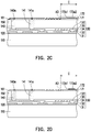
- FIG. 2A to FIG. 2F show cross sections of a manufacturing method of a substrate structure of another embodiment of the invention.
- FIG. 1A to FIG. 1I show cross sections of a manufacturing method of a substrate structure of an embodiment of the invention.
- FIG. 1I shows a perspective view of region A 2 in FIG. 1H .
- a first build-up circuit structure 130 is formed. Specifically, in the present embodiment, a glass substrate 110 is first provided, and a release layer 120 is formed on the glass substrate 110 . Next, the first build-up circuit structure 130 is formed according to the following steps. A first patterned circuit layer 131 is formed (such as via a photolithography method) on the release layer 120 , a first dielectric layer 132 is formed on the first patterned circuit layer 131 , drilling is performed on the first dielectric layer 132 (such as via a laser method) to expose a portion of the first patterned circuit layer 131 , at least one first conductive via 133 (FIG.
- first conductive via 133 penetrates first dielectric layer 132
- first patterned circuit layer 131 may be electrically connected to the second patterned circuit layer 134 via the first conductive via 133 .
- the release layer 120 is located between the first build-up circuit structure 130 and the glass substrate 110 .
- the material of the first dielectric layer 132 and the second dielectric layer 135 is, for example, a polymer material or a resin material.
- At least one copper pillar 140 and 141 ( FIG. 1C schematically shows two) is formed on the first build-up circuit structure 130 .
- drilling is first performed on the second dielectric layer 135 to expose a portion of the second patterned circuit layer 134 , for example.
- Another example is to form the at least one copper pillar 140 on a portion of the second patterned circuit layer 134 exposed by the first build-up circuit structure 130 via a photolithography method.
- the heights of the copper pillars 140 and 141 may be the same or different.
- a dielectric layer 150 is formed on the first build-up circuit structure 130 , and the dielectric layer 150 wraps the copper pillars 140 and 141 .
- the dielectric layer 150 is formed on the first build-up circuit structure 130 such that the dielectric layer 150 covers the second dielectric layer 135 and the dielectric layer 150 wraps the sides of the copper pillars 140 and 141 or completely wraps the copper pillars 140 and 141 .
- polishing is performed via, for example, a chemical mechanical polishing method to expose upper surfaces 140 a and 141 a of the copper pillars 140 and 141 and make the upper surfaces 140 a and 141 a of the copper pillars 140 and 141 level with the dielectric layer 150 .
- the dielectric layer 150 and the glass substrate 110 are respectively located at two opposite sides of the first build-up circuit structure 130 .
- the material of the dielectric layer 150 is, for example, a silicone material or a resin-mixed material.
- a second build-up circuit structure 160 and a capacitive element 170 are formed on the dielectric layer 150 .
- the third patterned circuit layer 161 is first formed on the dielectric layer 150 , wherein the third patterned circuit layer 161 covers the upper surfaces 140 a and 141 a of the copper pillars 140 and 141 , and then the capacitive element 170 is disposed in a capacitive element sitting region C on the dielectric layer 150 via an adhesive layer 180 .
- the capacitive element 170 is disposed between the fourth patterned circuit layer 164 and the dielectric layer 150 , and the capacitive element 170 is level with the patterned circuit layer 161 .
- FIG. 1F shows an enlarged view of region A 1 in FIG. 1E , wherein the capacitive element 170 includes a first electrode 171 , a fourth dielectric layer 172 , and a second electrode 173 .
- the first electrode 171 is disposed on the dielectric layer 150 .
- the fourth dielectric layer 172 is disposed on the first electrode 171 .
- the second electrode 173 is disposed on the fourth dielectric layer 172 .
- the second electrode 173 and the first electrode 171 are respectively located at two opposite sides of the fourth dielectric layer 172 .
- the material of the fourth dielectric layer 172 is, for example, silicon oxide or other insulating resins or a metal oxide material, and is preferably, for example, aluminium oxide.
- the material of the adhesive layer 180 is, for example, a viscous polymer material or resin material.
- a third dielectric layer 162 is formed on the third patterned circuit layer 161 , and the third dielectric layer 162 covers the third patterned circuit layer 161 and the capacitive element 170 .
- drilling is performed on the third dielectric layer 162 via, for example, a laser method to expose a portion of the third patterned circuit layer 161 , the second electrode 173 , and the first electrode 171 .
- a plurality of second conductive vias 163 ( FIG. 1G schematically shows three) are formed on the exposed portion of the third patterned circuit layer 161 , the second electrode 173 , and the first electrode 171 , and the second conductive vias 163 penetrate the third dielectric layer 162 .
- the fourth patterned circuit layer 164 is formed on the third dielectric layer 162 .
- the fourth patterned circuit layer 164 and the third patterned circuit layer 161 are respectively located at two opposite sides of the third dielectric layer 162 .
- the fourth patterned circuit layer 164 is electrically connected to the third patterned circuit layer 161 via the second conductive vias 163 .
- the fourth patterned circuit layer 164 is electrically connected to the capacitive element 170 via the second conductive vias 163 .
- the material of the third dielectric layer 162 is, for example, a polymer material or a resin material. At this point, the manufacture of the second build-up circuit structure 160 and the capacitive element 170 is completed.
- the capacitive element 170 formed is disposed on the dielectric layer 150 using the adhesive layer 180 , the invention is not limited thereto. In other words, in other embodiments, a capacitive element may also be manufactured on the dielectric layer 150 using a semiconductor process.
- a patterned solder mask 190 is formed on the second build-up circuit structure 160 , and the release layer 120 and the glass substrate 110 are separated to form the substrate structure 100 .
- the patterned solder mask 190 is formed on the second build-up circuit structure 160 such that the patterned solder mask 190 and the dielectric layer 150 are respectively located at two opposite sides of the second build-up circuit structure 160 .
- the patterned solder mask 190 covers the third dielectric layer 162 and exposes a portion of the fourth patterned circuit layer 164 .
- the release layer 120 and the glass substrate 110 are separated to complete the manufacture of the substrate structure 100 .
- the second build-up circuit structure 160 and the first build-up circuit structure 130 are respectively located at two opposite sides of the dielectric layer 150 .
- the capacitive element 170 is disposed in the capacitive element setting region C within the second build-up circuit structure 160 .
- the copper pillars 140 and 141 penetrate the dielectric layer 150 .
- the copper pillars 140 and 141 are electrically connected to the second build-up circuit structure 160 and the first build-up circuit structure 130 .
- FIG. 1I shows a perspective view of region A 2 in FIG. 1H and omits the second dielectric layer 135 .
- the substrate structure 100 of the present embodiment may include both the inductive element 200 and the capacitive element 170 , wherein the inductive element 200 is disposed in the dielectric layer 150 , and the capacitive element 170 is disposed on the dielectric layer 150 .
- the substrate structure 100 of the present embodiment includes the first build-up circuit structure 130 , the dielectric layer 150 , the second build-up circuit structure 160 , the at least one copper pillar 140 and 141 , and the capacitive element 170 .
- the dielectric layer 150 is disposed on the first build-up circuit structure 130 .
- the second build-up circuit structure 160 is disposed on the dielectric layer 150 .
- the second build-up circuit structure 160 and the first build-up circuit structure 130 are respectively located at two opposite sides of the dielectric layer 150 .
- the copper pillars 140 and 141 penetrate the dielectric layer 150 and are electrically connected to the second build-up circuit structure 160 and the first build-up circuit structure 130 .
- the capacitive element 170 is disposed in the capacitive element setting region C within the second build-up circuit structure 160 .
- FIG. 2A to FIG. 2F show cross-sections of a manufacturing method of a substrate structure of another embodiment of the invention.
- the manufacturing method of the substrate structure of the present embodiment is similar to the manufacturing method of the substrate structure in FIG. 1A to FIG. 1I , and the main difference between the two is that: in the present embodiment, a capacitive element 170 a is manufactured on the dielectric layer 150 via a semiconductor process.
- the first build-up circuit structure 130 the copper pillars 140 and 141 , and the dielectric layer 150 are manufactured according to the steps of FIG. 1A to FIG. 1D .
- FIG. 2E shows an enlarged view of region A 3 in FIG. 2D .
- a first electrode 171 is formed on the dielectric layer 150 at the same time of forming the third patterned circuit layer 161 , wherein the first electrode 171 is disposed in the capacitive element setting region C.
- a fourth dielectric layer 172 is formed on the first electrode 171 via, for example, a chemical vapor deposition method, and the fourth dielectric layer 172 covers the third patterned circuit layer 161 , the dielectric layer 150 , and the first electrode 171 .
- a titanium layer 173 a 1 and a copper layer 173 a 2 are sequentially formed on the fourth dielectric layer 172 via, for example, a sputtering method. Then, a portion of the titanium layer 173 a 1 , the copper layer 173 a 2 , and the fourth dielectric layer 172 are removed to form the capacitive element 170 a .
- the titanium layer 173 a 1 and the copper layer 173 a 2 can be used as a second electrode 173 a of the capacitive element 170 a .
- the copper layer 173 a 2 and the fourth dielectric layer 172 are respectively located at two opposite sides of the titanium layer 173 a 1 .
- the second build-up circuit structure 160 and the patterned solder mask 190 are manufactured according to the steps of FIG. 1G to FIG. 1I , and the release layer 120 and the glass substrate 110 are separated to complete the manufacture of the substrate structure 100 a of the present embodiment, as shown in FIG. 2F .
- a first build-up circuit structure, a copper pillar, a dielectric layer, a second build-up circuit structure, and a capacitive element are sequentially formed.
- the second build-up circuit structure and the first build-up circuit structure are respectively located at two opposite sides of the dielectric layer.
- the capacitive element is disposed in the capacitive element setting region within the second build-up circuit structure.
- the copper pillar penetrates the dielectric layer and is electrically connected to the second build-up circuit structure and the first build-up circuit structure.
- the substrate structure of the present embodiment may include an inductive element and a capacitive element simultaneously, wherein the inductive element is disposed in the dielectric layer, and the capacitive element is disposed on the dielectric layer. Therefore, compared to the prior art in which the conductive via of the inductive element is formed in the glass substrate, the substrate structure and the manufacturing method thereof of the invention have the advantages of simplified process, lowered cost, and increased yield.
Landscapes
- Engineering & Computer Science (AREA)
- Power Engineering (AREA)
- Computer Hardware Design (AREA)
- Microelectronics & Electronic Packaging (AREA)
- Physics & Mathematics (AREA)
- Condensed Matter Physics & Semiconductors (AREA)
- General Physics & Mathematics (AREA)
- Ceramic Engineering (AREA)
- Chemical & Material Sciences (AREA)
- Manufacturing & Machinery (AREA)
- Production Of Multi-Layered Print Wiring Board (AREA)
Priority Applications (1)
| Application Number | Priority Date | Filing Date | Title |
|---|---|---|---|
| US16/874,691 US10950687B2 (en) | 2018-08-29 | 2020-05-15 | Manufacturing method of substrate structure |
Applications Claiming Priority (3)
| Application Number | Priority Date | Filing Date | Title |
|---|---|---|---|
| TW107130092A | 2018-08-29 | ||
| TW107130092A TWI663633B (zh) | 2018-08-29 | 2018-08-29 | 基板結構及其製作方法 |
| TW107130092 | 2018-08-29 |
Related Child Applications (1)
| Application Number | Title | Priority Date | Filing Date |
|---|---|---|---|
| US16/874,691 Division US10950687B2 (en) | 2018-08-29 | 2020-05-15 | Manufacturing method of substrate structure |
Publications (2)
| Publication Number | Publication Date |
|---|---|
| US20200075711A1 US20200075711A1 (en) | 2020-03-05 |
| US10700161B2 true US10700161B2 (en) | 2020-06-30 |
Family
ID=67764267
Family Applications (2)
| Application Number | Title | Priority Date | Filing Date |
|---|---|---|---|
| US16/159,726 Active US10700161B2 (en) | 2018-08-29 | 2018-10-15 | Substrate structure and manufacturing method thereof |
| US16/874,691 Active US10950687B2 (en) | 2018-08-29 | 2020-05-15 | Manufacturing method of substrate structure |
Family Applications After (1)
| Application Number | Title | Priority Date | Filing Date |
|---|---|---|---|
| US16/874,691 Active US10950687B2 (en) | 2018-08-29 | 2020-05-15 | Manufacturing method of substrate structure |
Country Status (2)
| Country | Link |
|---|---|
| US (2) | US10700161B2 (zh) |
| TW (1) | TWI663633B (zh) |
Families Citing this family (1)
| Publication number | Priority date | Publication date | Assignee | Title |
|---|---|---|---|---|
| TWI789151B (zh) * | 2021-12-09 | 2023-01-01 | 恆勁科技股份有限公司 | 電子封裝件及其製法 |
Citations (5)
| Publication number | Priority date | Publication date | Assignee | Title |
|---|---|---|---|---|
| US20110062549A1 (en) * | 2009-09-11 | 2011-03-17 | Stats Chippac, Ltd. | Semiconductor Device and Method of Forming Integrated Passive Device |
| US20150035162A1 (en) | 2013-08-02 | 2015-02-05 | Qualcomm Incorporated | Inductive device that includes conductive via and metal layer |
| US20170103946A1 (en) * | 2015-10-07 | 2017-04-13 | Advanced Semiconductor Engineering, Inc. | Semiconductor device and method for manufacturing the same |
| US20170345726A1 (en) * | 2016-05-27 | 2017-11-30 | Taiwan Semiconductor Manufacturing Company, Ltd. | Testing, Manufacturing, and Packaging Methods for Semiconductor Devices |
| US20180261665A1 (en) * | 2016-12-28 | 2018-09-13 | Noda Screen Co., Ltd. | Thin film capacitor and semiconductor device |
Family Cites Families (4)
| Publication number | Priority date | Publication date | Assignee | Title |
|---|---|---|---|---|
| US7027289B2 (en) * | 2004-03-25 | 2006-04-11 | Intel Corporation | Extended thin film capacitor (TFC) |
| US9331057B2 (en) * | 2007-10-26 | 2016-05-03 | Infineon Technologies Ag | Semiconductor device |
| US9978729B2 (en) * | 2015-03-06 | 2018-05-22 | Mediatek Inc. | Semiconductor package assembly |
| US9922964B1 (en) * | 2016-09-19 | 2018-03-20 | Taiwan Semiconductor Manufacturing Co., Ltd. | Package structure with dummy die |
-
2018
- 2018-08-29 TW TW107130092A patent/TWI663633B/zh active
- 2018-10-15 US US16/159,726 patent/US10700161B2/en active Active
-
2020
- 2020-05-15 US US16/874,691 patent/US10950687B2/en active Active
Patent Citations (5)
| Publication number | Priority date | Publication date | Assignee | Title |
|---|---|---|---|---|
| US20110062549A1 (en) * | 2009-09-11 | 2011-03-17 | Stats Chippac, Ltd. | Semiconductor Device and Method of Forming Integrated Passive Device |
| US20150035162A1 (en) | 2013-08-02 | 2015-02-05 | Qualcomm Incorporated | Inductive device that includes conductive via and metal layer |
| US20170103946A1 (en) * | 2015-10-07 | 2017-04-13 | Advanced Semiconductor Engineering, Inc. | Semiconductor device and method for manufacturing the same |
| US20170345726A1 (en) * | 2016-05-27 | 2017-11-30 | Taiwan Semiconductor Manufacturing Company, Ltd. | Testing, Manufacturing, and Packaging Methods for Semiconductor Devices |
| US20180261665A1 (en) * | 2016-12-28 | 2018-09-13 | Noda Screen Co., Ltd. | Thin film capacitor and semiconductor device |
Also Published As
| Publication number | Publication date |
|---|---|
| US10950687B2 (en) | 2021-03-16 |
| TW202009983A (zh) | 2020-03-01 |
| US20200075711A1 (en) | 2020-03-05 |
| US20200273948A1 (en) | 2020-08-27 |
| TWI663633B (zh) | 2019-06-21 |
Similar Documents
| Publication | Publication Date | Title |
|---|---|---|
| JP4166013B2 (ja) | 薄膜キャパシタ製造方法 | |
| DE102015112980B4 (de) | In gehäusesubstrate eingebettete dünnfilmkondensatoren und verfahren zur integration eingebetteter dünnfilmkondensatoren in gehäusesubstrate | |
| JP2019106429A (ja) | ガラス配線基板、その製造方法及び半導体装置 | |
| JP6441269B2 (ja) | 積層薄膜キャパシタ | |
| JP6614246B2 (ja) | キャパシタ内蔵多層配線基板及びその製造方法 | |
| US9257221B2 (en) | Through-hole via inductor in a high-frequency device | |
| US9449762B2 (en) | Embedded package substrate capacitor with configurable/controllable equivalent series resistance | |
| KR20220116560A (ko) | 박막 캐패시터 및 이것을 구비하는 전자 회로 기판 | |
| US10950687B2 (en) | Manufacturing method of substrate structure | |
| US20070077687A1 (en) | Method of producing circuit carriers with integrated passive components | |
| JP2017139422A (ja) | 電子部品 | |
| CN112310047B (zh) | 电容集成结构及其电容 | |
| US9117693B2 (en) | Passive integrated circuit | |
| TWI643534B (zh) | 線路板結構及其製作方法 | |
| JP2006510233A (ja) | 低インダクタンス埋め込みキャパシタを有するプリント配線板およびその製造方法 | |
| US8884717B2 (en) | Diplexer | |
| CN110890316B (zh) | 基板结构及其制作方法 | |
| JP2006196811A (ja) | コンデンサおよびそれを用いた複合部品 | |
| US20070293014A1 (en) | Method for forming metal-insulator-metal capacitor of semiconductor device | |
| JP6764658B2 (ja) | 電子部品 | |
| CN108550531B (zh) | 封装基板的制造方法 | |
| KR102538911B1 (ko) | 인덕터 | |
| CN111403602A (zh) | 垂直电容器结构、电容器组件,以及制造所述垂直电容器结构的方法 | |
| KR101680283B1 (ko) | 표면 실장 인덕터 소자 및 이를 포함하는 rf 집적 회로 | |
| CN108682630B (zh) | 封装基板的制造方法 |
Legal Events
| Date | Code | Title | Description |
|---|---|---|---|
| FEPP | Fee payment procedure |
Free format text: ENTITY STATUS SET TO UNDISCOUNTED (ORIGINAL EVENT CODE: BIG.); ENTITY STATUS OF PATENT OWNER: LARGE ENTITY |
|
| AS | Assignment |
Owner name: UNIMICRON TECHNOLOGY CORP., TAIWAN Free format text: ASSIGNMENT OF ASSIGNORS INTEREST;ASSIGNORS:CHEN, YU-HUA;CHEN, FU-YANG;CHIEN, CHUN-HSIEN;AND OTHERS;SIGNING DATES FROM 20180928 TO 20181001;REEL/FRAME:047204/0879 |
|
| STPP | Information on status: patent application and granting procedure in general |
Free format text: NOTICE OF ALLOWANCE MAILED -- APPLICATION RECEIVED IN OFFICE OF PUBLICATIONS |
|
| STCF | Information on status: patent grant |
Free format text: PATENTED CASE |
|
| MAFP | Maintenance fee payment |
Free format text: PAYMENT OF MAINTENANCE FEE, 4TH YEAR, LARGE ENTITY (ORIGINAL EVENT CODE: M1551); ENTITY STATUS OF PATENT OWNER: LARGE ENTITY Year of fee payment: 4 |