US10692454B2 - Gate driver on array having a circuit start signal applied to a pull-down maintenance module - Google Patents
Gate driver on array having a circuit start signal applied to a pull-down maintenance module Download PDFInfo
- Publication number
- US10692454B2 US10692454B2 US15/742,886 US201715742886A US10692454B2 US 10692454 B2 US10692454 B2 US 10692454B2 US 201715742886 A US201715742886 A US 201715742886A US 10692454 B2 US10692454 B2 US 10692454B2
- Authority
- US
- United States
- Prior art keywords
- signal
- tft
- node
- goa
- low voltage
- Prior art date
- Legal status (The legal status is an assumption and is not a legal conclusion. Google has not performed a legal analysis and makes no representation as to the accuracy of the status listed.)
- Active, expires
Links
- 238000012423 maintenance Methods 0.000 title claims abstract description 48
- 230000000630 rising effect Effects 0.000 claims description 15
- 239000003990 capacitor Substances 0.000 claims description 12
- 238000004519 manufacturing process Methods 0.000 abstract description 8
- 238000000034 method Methods 0.000 description 8
- 239000004973 liquid crystal related substance Substances 0.000 description 5
- 239000000758 substrate Substances 0.000 description 5
- 230000000694 effects Effects 0.000 description 2
- XUIMIQQOPSSXEZ-UHFFFAOYSA-N Silicon Chemical compound [Si] XUIMIQQOPSSXEZ-UHFFFAOYSA-N 0.000 description 1
- 229910021417 amorphous silicon Inorganic materials 0.000 description 1
- 230000004048 modification Effects 0.000 description 1
- 238000012986 modification Methods 0.000 description 1
- 230000005855 radiation Effects 0.000 description 1
- 229910052710 silicon Inorganic materials 0.000 description 1
- 239000010703 silicon Substances 0.000 description 1
- 239000010409 thin film Substances 0.000 description 1
- 238000002834 transmittance Methods 0.000 description 1
Images




Classifications
-
- G—PHYSICS
- G09—EDUCATION; CRYPTOGRAPHY; DISPLAY; ADVERTISING; SEALS
- G09G—ARRANGEMENTS OR CIRCUITS FOR CONTROL OF INDICATING DEVICES USING STATIC MEANS TO PRESENT VARIABLE INFORMATION
- G09G3/00—Control arrangements or circuits, of interest only in connection with visual indicators other than cathode-ray tubes
- G09G3/20—Control arrangements or circuits, of interest only in connection with visual indicators other than cathode-ray tubes for presentation of an assembly of a number of characters, e.g. a page, by composing the assembly by combination of individual elements arranged in a matrix no fixed position being assigned to or needed to be assigned to the individual characters or partial characters
- G09G3/34—Control arrangements or circuits, of interest only in connection with visual indicators other than cathode-ray tubes for presentation of an assembly of a number of characters, e.g. a page, by composing the assembly by combination of individual elements arranged in a matrix no fixed position being assigned to or needed to be assigned to the individual characters or partial characters by control of light from an independent source
- G09G3/36—Control arrangements or circuits, of interest only in connection with visual indicators other than cathode-ray tubes for presentation of an assembly of a number of characters, e.g. a page, by composing the assembly by combination of individual elements arranged in a matrix no fixed position being assigned to or needed to be assigned to the individual characters or partial characters by control of light from an independent source using liquid crystals
- G09G3/3611—Control of matrices with row and column drivers
- G09G3/3674—Details of drivers for scan electrodes
- G09G3/3677—Details of drivers for scan electrodes suitable for active matrices only
-
- G—PHYSICS
- G09—EDUCATION; CRYPTOGRAPHY; DISPLAY; ADVERTISING; SEALS
- G09G—ARRANGEMENTS OR CIRCUITS FOR CONTROL OF INDICATING DEVICES USING STATIC MEANS TO PRESENT VARIABLE INFORMATION
- G09G2310/00—Command of the display device
- G09G2310/02—Addressing, scanning or driving the display screen or processing steps related thereto
- G09G2310/0264—Details of driving circuits
-
- G—PHYSICS
- G09—EDUCATION; CRYPTOGRAPHY; DISPLAY; ADVERTISING; SEALS
- G09G—ARRANGEMENTS OR CIRCUITS FOR CONTROL OF INDICATING DEVICES USING STATIC MEANS TO PRESENT VARIABLE INFORMATION
- G09G2310/00—Command of the display device
- G09G2310/02—Addressing, scanning or driving the display screen or processing steps related thereto
- G09G2310/0264—Details of driving circuits
- G09G2310/0286—Details of a shift registers arranged for use in a driving circuit
-
- G—PHYSICS
- G09—EDUCATION; CRYPTOGRAPHY; DISPLAY; ADVERTISING; SEALS
- G09G—ARRANGEMENTS OR CIRCUITS FOR CONTROL OF INDICATING DEVICES USING STATIC MEANS TO PRESENT VARIABLE INFORMATION
- G09G2310/00—Command of the display device
- G09G2310/06—Details of flat display driving waveforms
- G09G2310/061—Details of flat display driving waveforms for resetting or blanking
Definitions
- the present invention relates to the field of display techniques, and in particular to a gate driver on array (GOA) circuit.
- GOA gate driver on array
- the liquid crystal display provides many advantages, such as thinness, low power-consumption and no radiation, and is widely used in, such as, LCD televisions, mobile phones, personal digital assistants (PDAs), digital cameras, computer screens, laptop screens, and so on.
- LCD liquid crystal display
- PDAs personal digital assistants
- the LCD technology also dominates the field of panel displays.
- LCDs on the current market are of backlight type, which comprises an LCD panel and a backlight module.
- the operation theory behind LCD is to inject the liquid crystal (LC) molecules between a thin film transistor (TFT) array substrate and a color filter (CF) substrate, and applies a driving voltage between the two substrates to control the rotation direction of the LC molecules to refract the light from the backlight module to generate the image on the display.
- TFT thin film transistor
- CF color filter
- each pixel is electrically connected to a TFT, with a gate (Gate) connected to a horizontal scan line, a source (Source) connected to a data line in a vertical direction, and a drain (Drain) connected to a pixel electrode.
- Gate gate
- Source Source
- Drain drain
- the driving of the horizontal scan line of the current active LCD is mainly executed by an external integrated circuit (IC).
- the external IC can control the charge and discharge of the horizontal scan line in each stage progressively.
- the gate driver on array (GOA) technology i.e., the array substrate row driving technology, can use the array process of the LCD panel to manufacture the driver circuit of the horizontal scan lines on the substrate at area surrounding the active area to replace the external IC for driving the horizontal scan lines.
- the GOA technology can reduce the bonding process for external IC and has the opportunity to enhance yield rate and reduce production cost, as well as make the LCD panel more suitable for the production of narrow border display products.
- FIG. 1 shows a schematic view of a known GOA circuit.
- the GOA circuit comprises a plurality of cascaded GOA units, with each of the GOA units comprising a pull-up control module 100 ′, an output module 200 ′, a pull-down module 300 ′, a first pull-down maintenance module 400 ′, and a second pull-down maintenance module 550 ′.
- N For a positive integer N, except the first to the fourth GOA units and the last fourth to first GOA units, in the N-th GOA unit: the pull-up control module 100 ′ comprises an eleventh TFT T 11 ′, the eleventh TFT T 11 ′ has a gate connected to cascade-propagate signal ST(N ⁇ 4)′ of the fourth previous GOA unit (i.e.
- the output module 200 ′ comprises a twenty-first TFT T 21 ′, a twenty-second TFT T 22 ′ and a first capacitor C 1 ′;
- the twenty-first TFT T 21 ′ has a gate the first node Q(N)′, a source connected to a clock signal CK′, and a drain outputting a scan signal G(N)′;
- the twenty-second TFT T 22 ′ has a gate connected to the first node Q(N)′, a source clock signal CK′, and a drain outputting a cascade-propagate signal ST(N)′;
- the first capacitor C 1 ′ has one end connected to the first node Q(N)′ and the other end connected to the drain of the twenty-first TFT T 21 ′.
- the pull-down module 300 's comprises a forty-third TFT T 43 ′, the forty-third TFT 43 ′ has a gate connected to the fourth next GOA unit (i.e., (N+4)-th GOA unit), a source connected to the low voltage signal VSS, and a drain connected to the first node Q(N)′.
- the fourth next GOA unit i.e., (N+4)-th GOA unit
- the first pull-down maintenance module 400 ′ comprises a thirty-first TFT T 31 ′, a forty-first TFT T 41 ′, a fifty-first TFT T 51 ′ and a fifty-second TFT T 52 ′;
- the thirty-first TFT T 31 ′ has a gate connected to a second node P(N)′, a source connected to the low voltage signal VSS, and a drain connected to the drain of the twenty-first TFT T 21 ′;
- the forty-first TFT T 41 ′ has a gate connected to the second node P(N)′, a source connected to the low voltage signal VSS, and a drain connected to the first node Q(N)′;
- the fifty-first TFT T 51 ′ has a gate and a source connected to a first control signal LC 1 ′, and a drain connected to the second node P(N)′;
- the fifty-second TFT T 52 ′ has a gate connected to the first node Q(N)′,
- the second pull-down maintenance module 500 ′ comprises a thirty-second TFT T 32 ′, a forty-second TFT T 42 ′, a sixty-first TFT T 61 ′ and a sixty-second TFT T 62 ′;
- the thirty-second TFT T 32 ′ has a gate connected to a third node T(N)′, a source connected to the low voltage signal VSS, and a drain connected to the drain of the twenty-first TFT T 21 ′;
- the forty-second TFT T 42 ′ has a gate connected to the third node T(N)′, a source connected to the low voltage signal VSS, and a drain connected to the first node Q(N)′;
- the sixty-one TFT T 61 ′ has a gate and a source connected to a second control signal LC 2 ′, and a drain connected to the third node T(N)′;
- the sixty-second TFT T 62 ′ has a gate connected to the first node Q(N
- the first control signal LC 1 and the second control signal LC 2 have opposite phases.
- the eleventh TFT T 11 ′ is turned on to write the high voltage signal VDD to the first node Q(N)′ to control the twenty-first TFT T 21 ′ and the twenty-second TFT T 22 ′ to output respectively a scan signal G(N)′ corresponding to the clock signal CK′ and the cascade-propagate signal ST(N)′, while, at the same time, the fifty-second TFT T 52 ′ and the sixty-second TFT T 62 ′ are turned on to allow the low voltage signal VSS written into the gates of the forty-first TGT T 41 ′, forty-second TFT T 42 ′, thirty-first TFT T 31 ′, and thirty-second TFT T 32 ′.
- the gate-source voltage difference between the gates and the sources of the forty-first TGT T 41 ′, forty-second TFT T 42 ′, thirty-first TFT T 31 ′, and thirty-second TFT T 32 ′ are all 0, so as to turn off the forty-first TGT T 41 ′, forty-second TFT T 42 ′, thirty-first TFT T 31 ′, and thirty-second TFT T 32 ′ when the GOA unit is outputting the scan signal G(N)′ and the cascade-propagate signal ST(N)′.
- a gate-source voltage difference of 0 is not a point with the TFT smallest current leakage, which causes a leakage in the forty-first TFT T 41 ′ forty-second TFT T 42 ′, thirty-first TFT T 31 ′, and thirty-second TFT T 32 ′, and affects the voltage level of the first node Q(n)′.
- the current method is to use two low voltage signals with different voltage levels to make the gate of the TFT have a negative gate voltage to make the leakage current of the TFT smaller.
- this method requires additional signal lines, resulting in increased space for fanout layout, which is disadvantageous to narrow border design, increases the number of signals and increases the production cost.
- the object of the present invention is to provide a GOA circuit, able to reduce the current leakage of the TFT in the first pull-down module to prevent the current leakage from affecting the voltage level of the first node, and to improve the circuit stability without additional signal lines, able to facilitate production cost reduction and achieving narrow border design.
- the present invention provides a GOA circuit, which comprises a plurality of cascaded GOA units, with each GOA unit comprising: a pull-up control module, an output module, a pull-down module and a first pull-down maintenance module;
- N-th GOA unit for an positive integer N, except the first to the fourth GOA units and the last fourth to the last GOA units, in the N-th GOA unit:
- the pull-up control module receiving a cascade-propagate signal from (N ⁇ 4)-th GOA unit and a high voltage signal, connected to a first node, for pulling up voltage at the first node to the high voltage signal based on the cascade-propagate signal from (N ⁇ 4)-th GOA unit;
- the output module receiving clock signal and connected to the first node, for outputting a scan signal and a cascade-propagate signal under control by the voltage of the first node;
- the pull-down module receiving a scan signal from (N+4)-th GOA unit and a low voltage signal, and connected to the first node, for pulling down voltage at the first node to the low voltage signal under the control of the scan signal of the (N+4)-th GOA unit;
- the first pull-down maintenance module receiving a first control signal, the low voltage signal, the scan signal and a circuit start signal, connected to the first node, for maintaining the scan signal and the voltage of the first node at the low voltage signal after the pull-down module pulling down the voltage of the first node;
- the circuit start signal being a pulse signal, and the circuit start signal having a low voltage level lower than the low voltage signal.
- the first pull-down maintenance module comprises: a 31 st TFT, a 41 st TFT, a 51 st TFT and a 52 nd TFT;
- the 31 st TFT has a gate connected to a second node, a source connected to the low voltage signal, and a drain connected to the scan signal;
- the 41 st TFT has a gate connected to the second node, a source connected to the low voltage signal, and a drain connected to the first node;
- the 51 st TFT has a gate and a source connected to a first control signal, and a drain connected to the second node;
- the 52 nd TFT has a gate connected to the first node, a source connected to the circuit start signal, and a drain connected to the second node.
- each GOA unit further comprises a second pull-down maintenance module, other than the first to fourth GOA units, in the N-th GOA unit:
- the second pull-down maintenance module comprises: a 32 nd TFT, a 42 nd TFT, a 61 st TFT and a 62 nd TFT;
- the 32 nd TFT has a gate connected to a third node, a source connected to the low voltage signal, and a drain connected to the scan signal;
- the 42 nd TFT has a gate connected to the third node, a source connected to the low voltage signal, and a drain connected to the first node;
- the 61 st TFT has a gate and a source connected to a second control signal, and a drain connected to the third node;
- the 62 nd TFT has a gate connected to the first node, a source connected to the circuit start signal, and a drain connected to the third node;
- the first control signal and the second control signal have opposite phases.
- the clock signal comprises: a first clock signal, a second clock signal, a third clock signal, a fourth clock signal, a fifth clock signal, a sixth clock signal, a seventh clock signal, and an eight clock signal, outputted serially; for a non-negative integer X, the (1+8X)-th GOA unit, the (2+8X)-th GOA unit, the (3+8X)-th GOA unit, the (4+8X)-th GOA unit, the (5+8X)-th GOA unit, the (6+8X)-th GOA unit, the (7+8X)-th GOA unit, and the (8+8X)-th GOA unit respectively receive the first clock signal, the second clock signal, the third clock signal, the fourth clock signal, the fifth clock signal, the sixth clock signal, the seventh clock signal, and the eight clock signal;
- the clock signal has a duty cycle ratio of 0.4;
- the circuit start signal has a high voltage duration equal to 3/4 of the cycle of the clocks signal
- the circuit start signal has a rising edge earlier than the rising edge of the first clock signal, with a gap of 1/4 of the cycle of the clocks signal.
- the low voltage level of circuit start signal and the low voltage signal have a voltage difference of 1.5-2.5V.
- the low voltage level of circuit start signal is ⁇ 8 and the low voltage signal is ⁇ 6V.
- the pull-up control module comprises: an 11 th TFT; the 11 th TFT having a gate connected to the cascade-propagate signal from the (N ⁇ 4)-th GOA unit, a source connected to the high voltage signal, and a drain connected to the first node.
- the output module comprises: a 21 st TFT, a 22 nd TFT, and a capacitor; the 21 st TFT having a gate connected to the first node, a source connected to the clock signal, and a drain outputting the scan signal; the 22 nd TFT having a gate connected to the first node, a source connected to the clock signal, and a drain outputting the cascade-propagate signal; the capacitor having one end connected to the first node and the other end connected to the drain of the 21 st TFT.
- the pull-down module comprises: a 43 rd TFT, and the 43 rd TFT has a gate connected to scan signal of the (N+4)-th GOA unit, a source connected to the low voltage signal, and a drain connected to the first node;
- the pull-down module comprises: a 43 rd TFT, and the 43 rd TFT has a gate connected to the circuit start signal, a source connected to the low voltage signal, and a drain connected to the first node.
- the pull-up control module comprises: an 11 th TFT, and the 11 th TFT has a gate connected to the circuit start signal, a source connected to the high voltage signal, and a drain connected to the first node;
- the first pull-down maintenance module comprises: a 31 st TFT, a 41 st TFT, a 51 st TFT and a 52 nd TFT;
- the 31 st TFT has a gate connected to the second node, a source connected to the low voltage signal, and a drain connected to the scan signal;
- the 41 st TFT has a gate connected to the second node, a source connected to the low voltage signal, and a drain connected to the first node;
- the 51 st TFT has a gate and a source connected to the first control signal, and a drain connected to the second node;
- the 52 nd TFT has a gate connected to the first node, a source connected to the low voltage signal
- the present invention also provides GOA circuit, which comprises a plurality of cascaded GOA units, with each GOA unit comprising: a pull-up control module, an output module, a pull-down module and a first pull-down maintenance module;
- N-th GOA unit for an positive integer N, except the first to the fourth GOA units and the last fourth to the last GOA units, in the N-th GOA unit:
- the pull-up control module receiving a cascade-propagate signal from (N ⁇ 4)-th GOA unit and a high voltage signal, connected to a first node, for pulling up voltage at the first node to the high voltage signal based on the cascade-propagate signal from (N ⁇ 4)-th GOA unit;
- the output module receiving clock signal and connected to the first node, for outputting a scan signal and a cascade-propagate signal under control by the voltage of the first node;
- the pull-down module receiving a scan signal from (N+4)-th GOA unit and a low voltage signal, and connected to the first node, for pulling down voltage at the first node to the low voltage signal under the control of the scan signal of the (N+4)-th GOA unit;
- the first pull-down maintenance module receiving a first control signal, the low voltage signal, the scan signal and a circuit start signal, connected to the first node, for maintaining the scan signal and the voltage of the first node at the low voltage signal after the pull-down module pulling down the voltage of the first node;
- the circuit start signal being a pulse signal, and the circuit start signal having a low voltage level lower than the low voltage signal;
- the first pull-down maintenance module comprising: a 31 st TFT, a 41 st TFT, a 51 st TFT and a 52 nd TFT; the 31 st TFT having a gate connected to a second node, a source connected to the low voltage signal, and a drain connected to the scan signal; the 41 st TFT having a gate connected to the second node, a source connected to the low voltage signal, and a drain connected to the first node; the 51 st TFT having a gate and a source connected to a first control signal, and a drain connected to the second node; the 52 nd TFT having a gate connected to the first node, a source connected to the circuit start signal, and a drain connected to the second node;
- each GOA unit further comprising a second pull-down maintenance module, the second pull-down maintenance module comprising: other than the first to fourth GOA units, in the N-th GOA unit: a 32 nd TFT, a 42 nd TFT, a 61 st TFT and a 62 nd TFT; the 32 nd TFT having a gate connected to a third node, a source connected to the low voltage signal, and a drain connected to the scan signal; the 42 nd TFT having a gate connected to the third node, a source connected to the low voltage signal, and a drain connected to the first node; the 61 st TFT having a gate and a source connected to a second control signal, and a drain connected to the third node; the 62 nd TFT having a gate connected to the first node, a source connected to the circuit start signal, and a drain connected to the third node;
- the first control signal and the second control signal have opposite phases
- the clock signal comprising: a first clock signal, a second clock signal, a third clock signal, a fourth clock signal, a fifth clock signal, a sixth clock signal, a seventh clock signal, and an eight clock signal, outputted serially; for a non-negative integer X, the (1+8X)-th GOA unit, the (2+8X)-th GOA unit, the (3+8X)-th GOA unit, the (4+8X)-th GOA unit, the (5+8X)-th GOA unit, the (6+8X)-th GOA unit, the (7+8X)-th GOA unit, and the (8+8X)-th GOA unit respectively receive the first clock signal, the second clock signal, the third clock signal, the fourth clock signal, the fifth clock signal, the sixth clock signal, the seventh clock signal, and the eight clock signal;
- the clock signal has a duty cycle ratio of 0.4;
- the circuit start signal having a high voltage duration equal to 3/4 of the cycle of the clocks signal
- the circuit start signal having a rising edge earlier than the rising edge of the first clock signal, with a gap of 1/4 of the cycle of the clocks signal;
- the pull-up control module comprising: an 11 th TFT; the 11 th TFT having a gate connected to the cascade-propagate signal from the (N ⁇ 4)-th GOA unit, a source connected to the high voltage signal, and a drain connected to the first node.
- the output module comprising: a 21 st TFT, a 22 nd TFT, and a capacitor; the 21 st TFT having a gate connected to the first node, a source connected to the clock signal, and a drain outputting the scan signal; the 22 nd TFT having a gate connected to the first node, a source connected to the clock signal, and a drain outputting the cascade-propagate signal; the capacitor having one end connected to the first node and the other end connected to the drain of the 21 st TFT.
- the present invention provides the following advantages.
- the present invention provides a GOA circuit, and in the GOA circuit, other than the first to the fourth GOA units, each GOA unit: the first pull-down maintenance module receives the first control signal, low voltage signal, scan signal and circuit start signal, and is connected to the first node, wherein the 52 nd TFT of the first pull-down maintenance module has a gate connected to the first node, a source receives the circuit start signal, and a drain connected to the gates of the 31 st TFT and 41 st TFT so that when the first node is at high voltage, the gate-source voltage difference of the 31 st TFT and the 41 st TFT are both negative to effectively reduce the current leakage and prevent the current leakage from affecting the voltage of the first node, to improve the circuit stability without additional signal lines, able to facilitate production cost reduction and achieving narrow border design.
- FIG. 1 is a schematic view showing a known GOA circuit
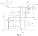
- FIG. 2 is a schematic view showing a circuit of the GOA circuit provided by the first embodiment of the present invention
- FIG. 3 is a schematic view showing a circuit of the first to the fourth GOA units of the GOA circuit provided by the embodiment of the present invention
- FIG. 4 is a schematic view showing a circuit of the last fourth to the last GOA units of the GOA circuit provided by the embodiment of the present invention.
- FIG. 5 is a schematic view showing the timing sequence for the GOA circuit by the embodiment of the present invention.
- the present invention provides a GOA circuit, which comprises: a plurality of cascaded GOA units, with each GOA unit comprising: a pull-up control module 100 , an output module 200 , a pull-down module 300 , and a first pull-down maintenance module 400 ;
- N-th GOA unit for an positive integer N, except the first to the fourth GOA units and the last fourth to the last GOA units, in the N-th GOA unit:
- the pull-up control module 100 receiving a cascade-propagate signal ST(N ⁇ 4) from (N ⁇ 4)-th GOA unit and a high voltage signal Vdd, connected to a first node Q(N), for pulling up voltage at the first node Q(N) to the high voltage signal Vdd based on the cascade-propagate signal ST(N ⁇ 4) from (N ⁇ 4)-th GOA unit.
- the pull-up control module 100 comprises: a 11 th TFT T 11 ; the 11 th TFT T 11 having a gate connected to the cascade-propagate signal ST(N ⁇ 4) from the (N ⁇ 4)-th GOA unit, a source connected to the high voltage signal Vdd, and a drain connected to the first node Q(N).
- the output module 200 receives clock signal CK and connected to the first node Q(N), for outputting a scan signal G(N) and a cascade-propagate signal ST(N) under control by the voltage of the first node Q(N).
- the output module 200 comprises: a 21 st TFT T 21 , a 22 nd TFT T 22 , and a capacitor C 1 ; the 21 st TFT T 21 having a gate connected to the first node Q(N), a source connected to the clock signal CK, and a drain outputting the scan signal G(N); the 22 nd TFT T 22 having a gate connected to the first node Q(N), a source connected to the clock signal CK, and a drain outputting the cascade-propagate signal ST(N); the capacitor having one end connected to the first node Q(N) and the other end connected to the drain of the 21 st TFT T 21 .
- the pull-down module 300 receives a scan signal G(N+4) from (N+4)-th GOA unit and a low voltage signal Vss, and connected to the first node Q(N), for pulling down voltage at the first node Q(N) to the low voltage signal Vss under the control of the scan signal G(N+4) of the (N+4)-th GOA unit;
- the first pull-down maintenance module 400 receives a first control signal LC 1 , the low voltage signal Vss, the scan signal G(N) and a circuit start signal STV, and is connected to the first node Q(N), for maintaining the scan signal G(N) and the voltage of the first node Q(N) at the low voltage signal Vss after the pull-down module 300 pulling down the voltage of the first node Q(N);
- the circuit start signal STV is a pulse signal, and the circuit start signal STV has a low voltage level lower than the low voltage signal Vss.
- the first pull-down maintenance module 400 comprises: a 31 st TFT T 31 , a 41 st TFT T 41 , a 51 st TFT T 51 and a 52 nd TFT T 52 ;
- the 31 st TFT T 31 has a gate connected to a second node P(N), a source connected to the low voltage signal Vss, and a drain connected to the scan signal G(N);
- the 41 st TFT T 41 has a gate connected to the second node P(N), a source connected to the low voltage signal Vss, and a drain connected to the first node Q(N);
- the 51 st TFT T 51 has a gate and a source connected to a first control signal LC 1 , and a drain connected to the second node P(N);
- the 52 nd TFT T 52 has a gate connected to the first node Q(N), a source connected to the circuit start signal STV,
- Each GOA unit further comprises a second pull-down maintenance module 500 .
- the second pull-down module 500 and the first pull-down module 400 operate alternatingly to maintain the scan signal and the voltage level at the first node Q(N) at the low voltage signal Vss after the pull-down module 300 pulls down the voltage level at the first node Q(N) to the low voltage signal Vss.
- the second pull-down maintenance module 500 comprises: a 32 nd TFT T 32 , a 42 nd TFT T 42 , a 61 st TFT T 61 and a 62 nd TFT T 62 ;
- the 32 nd TFT T 32 has a gate connected to a third node T(N), a source connected to the low voltage signal Vss, and a drain connected to the scan signal G(N);
- the 42 nd TFT T 42 has a gate connected to the third node T(N), a source connected to the low voltage signal Vss, and a drain connected to the first node Q(N);
- the 61 st TFT T 61 has a gate and a source connected to a second control signal LC 2 , and a drain connected to the third node T(N);
- the 62 nd TFT T 62 has a gate connected to the first node Q(N), a source connected to the circuit start
- the clock signal CK comprises: a first clock signal CK 1 , a second clock signal CK 2 , a third clock signal CK 3 , a fourth clock signal CK 4 , a fifth clock signal CK 5 , a sixth clock signal CK 6 , a seventh clock signal CK 7 , and an eight clock signal CK 8 , outputted serially; for a non-negative integer X, the (1+8X)-th GOA unit, the (2+8X)-th GOA unit, the (3+8X)-th GOA unit, the (4+8X)-th GOA unit, the (5+8X)-th GOA unit, the (6+8X)-th GOA unit, the (7+8X)-th GOA unit, and the (8+8X)-th GOA unit respectively receive the first clock signal CK 1 , the second clock signal CK 2 , the third clock signal CK 3 , the fourth clock signal CK 4 , the fifth clock signal CK 5 , the sixth clock signal CK 6
- the low voltage level of circuit start signal STV and the low voltage signal Vss have a voltage difference of 1.5-2.5V.
- the low voltage level of circuit start signal STV is ⁇ 8 and the low voltage signal Vss is ⁇ 6V.
- the pull-up control module 100 comprises: an 11 th TFT T 11 , and the 11 th TFT T 11 has a gate connected to the circuit start signal STV, a source connected to the high voltage signal Vdd, and a drain connected to the first node Q(N);
- the first pull-down maintenance module 400 comprises: a 31 st TFT T 31 , a 41 st TFT T 41 , a 51 st TFT T 51 and a 52 nd TFT T 52 ;
- the 31 st TFT T 31 has a gate connected to the second node P(N), a source connected to the low voltage signal Vss, and a drain connected to the scan signal G(N);
- the 41 st TFT T 41 has a gate connected to the second node P(N), a source connected to the low voltage signal Vss, and a drain connected to the first node Q(N);
- the 51 st TFT T 51 has a gate and a source connected to the first control signal
- the pull-down module 300 comprises: a 43 rd TFT T 43 , and the 43 rd TFT T 43 has a gate connected to the circuit start signal STV, a source connected to the low voltage signal Vss, and a drain connected to the first node Q(N); and the pull-up control module 100 , output module 200 , first pull-down module 400 , and second pull-down module 500 are all the same as the pull-up control module 100 , output module 200 , first pull-down module 400 , and second pull-down module 500 in the fifth to last fifth GOA units.
- the operation of the GOA circuit of the present invention is as follows: the circuit start signal STV first provides a high voltage, the 11 th TFT T 11 in the first to the fourth GOA units are turned on, and the voltage at the first node Q(N) in the first to the fourth GOA units rises to the high voltage, the 21 st TFT T 21 and the 22 nd TFT T 22 in the first to the fourth GOA units are both turned on, and then the first clock signal CK 1 outputs a high voltage.
- the first GOA unit outputs the scan signal and the cascade-propagate signal; then, the second clock signal CK 2 outputs the high voltage, and the second GOA unit outputs the scan signal and the cascade-propagate signal; then, the third clock signal CK 3 outputs the high voltage, and the third GOA unit outputs the scan signal and the cascade-propagate signal; and then, the fourth clock signal CK 4 outputs the high voltage, and the fourth GOA unit outputs the scan signal and the cascade-propagate signal.
- the cascade-propagate signals from the first GOA unit, the second GOA unit, the third GOA unit, and the fourth GOA unit are passed respectively to the pull-up control module 100 of the fifth GOA unit, the sixth GOA unit, the seventh GOA unit, the eighth GOA unit.
- the 11 th TFT T 11 of the fifth GOA unit, the sixth GOA unit, the seventh GOA unit, and the eighth GOA unit is turned on serially, and the fifth clock signal CK 5 , the sixth clock signal CK 6 , the seventh clock signal CK 7 , and the eighth clock signal CK 8 serially start to provide a high voltage, and the fifth GOA unit, the sixth GOA unit, the seventh GOA unit, and the eighth GOA unit respectively output the scan signal and the cascade-propagate signal during the time when the fifth clock signal CK 5 , the sixth clock signal CK 6 , the seventh clock signal CK 7 , and the eighth clock signal CK 8 are at high voltage.
- the pull-down module 300 of the first GOA unit, the second GOA unit, the third GOA unit, and the fourth GOA unit respectively receives the scan signal from the fifth GOA unit, the sixth GOA unit, the seventh GOA unit, and the eighth GOA unit, and correspondingly pull-down the first GOA unit, the second GOA unit, the third GOA unit, and the fourth GOA Unit to the voltage level of the low voltage signal Vss, and then the first pull-down maintenance module 400 or the second pull-down maintenance module 500 maintains the first node and the scan signal at the voltage level of the low voltage signal Vss, and so on, until the last fourth GOA unit, the last third GOA unit, the lasts second GOA unit, and the last GOA unit serially output the scan signal and the cascade-propagate signal, and the circuit start signal STV again provides a high voltage to the pull-down module 300 of the last fourth GOA unit, the last third GOA unit, the last second GOA unit, and the last GOA unit to pull-down the first node
- the high voltage signal Vdd charges the first node Q(N) to reach the high voltage.
- the 52 nd TFT T 52 and the 62 nd TFT T 62 controlled by the first node Q(N) are turned on, so that the low voltage of the circuit start signal STV is inputted to the gates of the 41 st TFT T 41 , 31 st TFT T 31 , 42 nd TFT T 42 , and 41 st TFT T 41 , and the sources of the 41 st TFT T 41 , 31 st TFT T 31 , 42 nd TFT T 42 , and 41 st TFT T 41 are all connected to the low voltage signal Vss.
- the gate-source voltage differences of the 41 st TFT T 41 , 31 st TFT T 31 , 42 nd TFT T 42 , and 41 st TFT T 41 are all negative when the first node Q(N) is high, which can effectively reduce the leakage current of the 41 st TFT T 41 , 31 st TFT T 31 , 42 nd TFT T 42 , and 41 st TFT T 41 , prevent the leakage current from affecting the voltage of the first node Q(N), improve the circuit stability without additional signal lines, and can reduce product costs and achieve narrow border design.
- the present invention provides a GOA circuit, and in the GOA circuit, other than the first to the fourth GOA units, each GOA unit: the first pull-down maintenance module receives the first control signal, low voltage signal, scan signal and circuit start signal, and is connected to the first node, wherein the 52 nd TFT of the first pull-down maintenance module has a gate connected to the first node, a source receives the circuit start signal, and a drain connected to the gates of the 31 st TFT and 41 st TFT so that when the first node is at high voltage, the gate-source voltage difference of the 31 st TFT and the 41 st TFT are both negative to effectively reduce the current leakage and prevent the current leakage from affecting the voltage of the first node, to improve the circuit stability without additional signal lines, able to facilitate production cost reduction and achieving narrow border design.
Landscapes
- Engineering & Computer Science (AREA)
- Chemical & Material Sciences (AREA)
- Crystallography & Structural Chemistry (AREA)
- Physics & Mathematics (AREA)
- Computer Hardware Design (AREA)
- General Physics & Mathematics (AREA)
- Theoretical Computer Science (AREA)
- Control Of Indicators Other Than Cathode Ray Tubes (AREA)
- Liquid Crystal Display Device Control (AREA)
- Shift Register Type Memory (AREA)
Applications Claiming Priority (4)
| Application Number | Priority Date | Filing Date | Title |
|---|---|---|---|
| CN201711132610.7 | 2017-11-15 | ||
| CN201711132610 | 2017-11-15 | ||
| CN201711132610.7A CN107705768B (zh) | 2017-11-15 | 2017-11-15 | Goa电路 |
| PCT/CN2017/116303 WO2019095484A1 (zh) | 2017-11-15 | 2017-12-15 | Goa电路 |
Publications (2)
| Publication Number | Publication Date |
|---|---|
| US20200105216A1 US20200105216A1 (en) | 2020-04-02 |
| US10692454B2 true US10692454B2 (en) | 2020-06-23 |
Family
ID=61180202
Family Applications (1)
| Application Number | Title | Priority Date | Filing Date |
|---|---|---|---|
| US15/742,886 Active 2038-11-06 US10692454B2 (en) | 2017-11-15 | 2017-12-15 | Gate driver on array having a circuit start signal applied to a pull-down maintenance module |
Country Status (3)
| Country | Link |
|---|---|
| US (1) | US10692454B2 (zh) |
| CN (1) | CN107705768B (zh) |
| WO (1) | WO2019095484A1 (zh) |
Families Citing this family (7)
| Publication number | Priority date | Publication date | Assignee | Title |
|---|---|---|---|---|
| TWI690931B (zh) * | 2019-03-08 | 2020-04-11 | 友達光電股份有限公司 | 閘極驅動電路以及移位暫存器的控制方法 |
| CN110827780B (zh) * | 2019-11-25 | 2021-01-26 | 成都中电熊猫显示科技有限公司 | 栅极驱动单元、栅极扫描驱动电路和液晶显示装置 |
| CN114792500A (zh) * | 2021-01-25 | 2022-07-26 | 深圳市柔宇科技股份有限公司 | 扫描信号线驱动电路、显示面板及电子设备 |
| CN113628596B (zh) * | 2021-07-23 | 2023-02-24 | 昆山龙腾光电股份有限公司 | 栅极驱动单元、栅极驱动电路及显示装置 |
| CN114187873B (zh) * | 2021-12-10 | 2023-05-30 | 武汉华星光电技术有限公司 | 栅极驱动电路及显示装置 |
| CN114882820A (zh) * | 2022-03-24 | 2022-08-09 | Tcl华星光电技术有限公司 | 栅极驱动电路和显示面板 |
| CN119317326B (zh) * | 2024-11-04 | 2025-11-14 | 武汉华星光电半导体显示技术有限公司 | 显示面板及显示装置 |
Citations (4)
| Publication number | Priority date | Publication date | Assignee | Title |
|---|---|---|---|---|
| US20150255014A1 (en) * | 2014-03-10 | 2015-09-10 | Au Optronics Corp. | Shift register group and method for driving the same |
| US20160140922A1 (en) * | 2014-11-13 | 2016-05-19 | Shenzhen China Star Optoelectronics Technology Co., Ltd. | Goa circuit and liquid crystal display device applied to liquid crystal displays |
| US20160284294A1 (en) * | 2014-07-15 | 2016-09-29 | Shenzhen China Star Optoelectronics Technology Co., Ltd. | Gate driving circuit applied for 2d-3d signal setting |
| CN106448590A (zh) | 2016-10-11 | 2017-02-22 | 深圳市华星光电技术有限公司 | 一种液晶显示面板的coa电路及显示装置 |
Family Cites Families (4)
| Publication number | Priority date | Publication date | Assignee | Title |
|---|---|---|---|---|
| TWI400686B (zh) * | 2009-04-08 | 2013-07-01 | Au Optronics Corp | 液晶顯示器之移位暫存器 |
| CN105185292B (zh) * | 2015-10-09 | 2017-11-07 | 昆山龙腾光电有限公司 | 栅极驱动电路及显示装置 |
| CN105427824B (zh) * | 2016-01-05 | 2016-11-30 | 京东方科技集团股份有限公司 | 具有漏电补偿模块的goa电路、阵列基板和显示面板 |
| CN107331360B (zh) * | 2017-08-14 | 2019-12-24 | 深圳市华星光电半导体显示技术有限公司 | Goa电路及液晶显示装置 |
-
2017
- 2017-11-15 CN CN201711132610.7A patent/CN107705768B/zh active Active
- 2017-12-15 WO PCT/CN2017/116303 patent/WO2019095484A1/zh not_active Ceased
- 2017-12-15 US US15/742,886 patent/US10692454B2/en active Active
Patent Citations (4)
| Publication number | Priority date | Publication date | Assignee | Title |
|---|---|---|---|---|
| US20150255014A1 (en) * | 2014-03-10 | 2015-09-10 | Au Optronics Corp. | Shift register group and method for driving the same |
| US20160284294A1 (en) * | 2014-07-15 | 2016-09-29 | Shenzhen China Star Optoelectronics Technology Co., Ltd. | Gate driving circuit applied for 2d-3d signal setting |
| US20160140922A1 (en) * | 2014-11-13 | 2016-05-19 | Shenzhen China Star Optoelectronics Technology Co., Ltd. | Goa circuit and liquid crystal display device applied to liquid crystal displays |
| CN106448590A (zh) | 2016-10-11 | 2017-02-22 | 深圳市华星光电技术有限公司 | 一种液晶显示面板的coa电路及显示装置 |
Also Published As
| Publication number | Publication date |
|---|---|
| WO2019095484A1 (zh) | 2019-05-23 |
| US20200105216A1 (en) | 2020-04-02 |
| CN107705768B (zh) | 2019-07-02 |
| CN107705768A (zh) | 2018-02-16 |
Similar Documents
| Publication | Publication Date | Title |
|---|---|---|
| US10692454B2 (en) | Gate driver on array having a circuit start signal applied to a pull-down maintenance module | |
| US10242637B2 (en) | CMOS GOA circuit | |
| US10741139B2 (en) | Goa circuit | |
| US10510314B2 (en) | GOA circuit having negative gate-source voltage difference of TFT of pull down module | |
| US10796656B1 (en) | GOA circuit | |
| US9659540B1 (en) | GOA circuit of reducing power consumption | |
| US9933889B2 (en) | GOA driving circuit | |
| US10043477B2 (en) | GOA circuit | |
| US9672784B2 (en) | CMOS gate driving circuit | |
| US9818363B2 (en) | Charging scan and charge sharing scan double output GOA circuit | |
| US9966025B1 (en) | Gate driving circuit | |
| US9786239B2 (en) | GOA circuit based on P-type thin film transistors | |
| US9799294B2 (en) | Liquid crystal display device and GOA scanning circuit of the same | |
| US9171516B2 (en) | Gate driver on array circuit | |
| US10311819B2 (en) | CMOS GOA circuit | |
| US10283067B2 (en) | GOA driving circuit and LCD | |
| US20200168170A1 (en) | Liquid crystal display device and driving method thereof | |
| US11158274B1 (en) | GOA circuit and liquid crystal display panel | |
| US10102820B2 (en) | GOA circuit | |
| US10283068B1 (en) | GOA circuit | |
| US10386663B2 (en) | GOA circuit and liquid crystal display device |
Legal Events
| Date | Code | Title | Description |
|---|---|---|---|
| AS | Assignment |
Owner name: SHENZHEN CHINA STAR OPTOELECTRONICS SEMICONDUCTOR DISPLAY TECHNOLOGY CO., LTD., CHINA Free format text: ASSIGNMENT OF ASSIGNORS INTEREST;ASSIGNORS:LV, XIAOWEN;CHOU, YIFANG;REEL/FRAME:045024/0556 Effective date: 20171226 |
|
| FEPP | Fee payment procedure |
Free format text: ENTITY STATUS SET TO UNDISCOUNTED (ORIGINAL EVENT CODE: BIG.); ENTITY STATUS OF PATENT OWNER: LARGE ENTITY |
|
| STPP | Information on status: patent application and granting procedure in general |
Free format text: NOTICE OF ALLOWANCE MAILED -- APPLICATION RECEIVED IN OFFICE OF PUBLICATIONS |
|
| STPP | Information on status: patent application and granting procedure in general |
Free format text: PUBLICATIONS -- ISSUE FEE PAYMENT VERIFIED |
|
| STCF | Information on status: patent grant |
Free format text: PATENTED CASE |
|
| MAFP | Maintenance fee payment |
Free format text: PAYMENT OF MAINTENANCE FEE, 4TH YEAR, LARGE ENTITY (ORIGINAL EVENT CODE: M1551); ENTITY STATUS OF PATENT OWNER: LARGE ENTITY Year of fee payment: 4 |