US10691040B2 - Abnormal discharge detection circuit for corona chargers - Google Patents
Abnormal discharge detection circuit for corona chargers Download PDFInfo
- Publication number
- US10691040B2 US10691040B2 US15/936,523 US201815936523A US10691040B2 US 10691040 B2 US10691040 B2 US 10691040B2 US 201815936523 A US201815936523 A US 201815936523A US 10691040 B2 US10691040 B2 US 10691040B2
- Authority
- US
- United States
- Prior art keywords
- abnormal discharge
- discharge detection
- circuit
- voltage
- charging
- Prior art date
- Legal status (The legal status is an assumption and is not a legal conclusion. Google has not performed a legal analysis and makes no representation as to the accuracy of the status listed.)
- Active
Links
- 230000002159 abnormal effect Effects 0.000 title claims abstract description 298
- 238000001514 detection method Methods 0.000 title claims abstract description 256
- 230000035945 sensitivity Effects 0.000 claims description 52
- 239000003990 capacitor Substances 0.000 description 27
- 238000000034 method Methods 0.000 description 20
- 230000008569 process Effects 0.000 description 20
- 239000003086 colorant Substances 0.000 description 14
- 230000007423 decrease Effects 0.000 description 11
- 238000007639 printing Methods 0.000 description 10
- 238000004804 winding Methods 0.000 description 10
- 238000010586 diagram Methods 0.000 description 8
- 102100022193 Glutamate receptor ionotropic, delta-1 Human genes 0.000 description 7
- 101000900493 Homo sapiens Glutamate receptor ionotropic, delta-1 Proteins 0.000 description 7
- 230000008859 change Effects 0.000 description 7
- 238000010438 heat treatment Methods 0.000 description 6
- 238000009499 grossing Methods 0.000 description 5
- 102100030684 Sphingosine-1-phosphate phosphatase 1 Human genes 0.000 description 4
- 101710168942 Sphingosine-1-phosphate phosphatase 1 Proteins 0.000 description 4
- 230000000694 effects Effects 0.000 description 4
- 101100165556 Mus musculus Bmp6 gene Proteins 0.000 description 3
- 230000015572 biosynthetic process Effects 0.000 description 3
- 230000015556 catabolic process Effects 0.000 description 3
- 230000003247 decreasing effect Effects 0.000 description 3
- 230000005684 electric field Effects 0.000 description 3
- 238000004519 manufacturing process Methods 0.000 description 3
- 239000000843 powder Substances 0.000 description 3
- 238000011109 contamination Methods 0.000 description 2
- 238000010891 electric arc Methods 0.000 description 2
- 230000005669 field effect Effects 0.000 description 2
- 230000010355 oscillation Effects 0.000 description 2
- 238000003825 pressing Methods 0.000 description 2
- WFKWXMTUELFFGS-UHFFFAOYSA-N tungsten Chemical compound [W] WFKWXMTUELFFGS-UHFFFAOYSA-N 0.000 description 2
- 229910052721 tungsten Inorganic materials 0.000 description 2
- 239000010937 tungsten Substances 0.000 description 2
- 101100256916 Caenorhabditis elegans sid-1 gene Proteins 0.000 description 1
- 101000654471 Mus musculus NAD-dependent protein deacetylase sirtuin-1 Proteins 0.000 description 1
- 230000009471 action Effects 0.000 description 1
- 230000005540 biological transmission Effects 0.000 description 1
- 238000004140 cleaning Methods 0.000 description 1
- 238000007599 discharging Methods 0.000 description 1
- 238000005516 engineering process Methods 0.000 description 1
- 239000000463 material Substances 0.000 description 1
- 239000000155 melt Substances 0.000 description 1
- 229910052751 metal Inorganic materials 0.000 description 1
- 239000002184 metal Substances 0.000 description 1
- 230000004044 response Effects 0.000 description 1
- 230000000087 stabilizing effect Effects 0.000 description 1
- 238000003860 storage Methods 0.000 description 1
Images


Classifications
-
- G—PHYSICS
- G03—PHOTOGRAPHY; CINEMATOGRAPHY; ANALOGOUS TECHNIQUES USING WAVES OTHER THAN OPTICAL WAVES; ELECTROGRAPHY; HOLOGRAPHY
- G03G—ELECTROGRAPHY; ELECTROPHOTOGRAPHY; MAGNETOGRAPHY
- G03G15/00—Apparatus for electrographic processes using a charge pattern
- G03G15/02—Apparatus for electrographic processes using a charge pattern for laying down a uniform charge, e.g. for sensitising; Corona discharge devices
- G03G15/0266—Arrangements for controlling the amount of charge
-
- G—PHYSICS
- G03—PHOTOGRAPHY; CINEMATOGRAPHY; ANALOGOUS TECHNIQUES USING WAVES OTHER THAN OPTICAL WAVES; ELECTROGRAPHY; HOLOGRAPHY
- G03G—ELECTROGRAPHY; ELECTROPHOTOGRAPHY; MAGNETOGRAPHY
- G03G15/00—Apparatus for electrographic processes using a charge pattern
- G03G15/02—Apparatus for electrographic processes using a charge pattern for laying down a uniform charge, e.g. for sensitising; Corona discharge devices
- G03G15/0258—Apparatus for electrographic processes using a charge pattern for laying down a uniform charge, e.g. for sensitising; Corona discharge devices provided with means for the maintenance of the charging apparatus, e.g. cleaning devices, ozone removing devices G03G15/0225, G03G15/0291 takes precedence
-
- G—PHYSICS
- G03—PHOTOGRAPHY; CINEMATOGRAPHY; ANALOGOUS TECHNIQUES USING WAVES OTHER THAN OPTICAL WAVES; ELECTROGRAPHY; HOLOGRAPHY
- G03G—ELECTROGRAPHY; ELECTROPHOTOGRAPHY; MAGNETOGRAPHY
- G03G15/00—Apparatus for electrographic processes using a charge pattern
- G03G15/02—Apparatus for electrographic processes using a charge pattern for laying down a uniform charge, e.g. for sensitising; Corona discharge devices
- G03G15/0283—Arrangements for supplying power to the sensitising device
-
- G—PHYSICS
- G03—PHOTOGRAPHY; CINEMATOGRAPHY; ANALOGOUS TECHNIQUES USING WAVES OTHER THAN OPTICAL WAVES; ELECTROGRAPHY; HOLOGRAPHY
- G03G—ELECTROGRAPHY; ELECTROPHOTOGRAPHY; MAGNETOGRAPHY
- G03G15/00—Apparatus for electrographic processes using a charge pattern
- G03G15/02—Apparatus for electrographic processes using a charge pattern for laying down a uniform charge, e.g. for sensitising; Corona discharge devices
- G03G15/0291—Apparatus for electrographic processes using a charge pattern for laying down a uniform charge, e.g. for sensitising; Corona discharge devices corona discharge devices, e.g. wires, pointed electrodes, means for cleaning the corona discharge device
-
- G—PHYSICS
- G03—PHOTOGRAPHY; CINEMATOGRAPHY; ANALOGOUS TECHNIQUES USING WAVES OTHER THAN OPTICAL WAVES; ELECTROGRAPHY; HOLOGRAPHY
- G03G—ELECTROGRAPHY; ELECTROPHOTOGRAPHY; MAGNETOGRAPHY
- G03G15/00—Apparatus for electrographic processes using a charge pattern
- G03G15/55—Self-diagnostics; Malfunction or lifetime display
-
- G—PHYSICS
- G01—MEASURING; TESTING
- G01R—MEASURING ELECTRIC VARIABLES; MEASURING MAGNETIC VARIABLES
- G01R19/00—Arrangements for measuring currents or voltages or for indicating presence or sign thereof
- G01R19/165—Indicating that current or voltage is either above or below a predetermined value or within or outside a predetermined range of values
- G01R19/16528—Indicating that current or voltage is either above or below a predetermined value or within or outside a predetermined range of values using digital techniques or performing arithmetic operations
-
- G—PHYSICS
- G03—PHOTOGRAPHY; CINEMATOGRAPHY; ANALOGOUS TECHNIQUES USING WAVES OTHER THAN OPTICAL WAVES; ELECTROGRAPHY; HOLOGRAPHY
- G03G—ELECTROGRAPHY; ELECTROPHOTOGRAPHY; MAGNETOGRAPHY
- G03G15/00—Apparatus for electrographic processes using a charge pattern
- G03G15/50—Machine control of apparatus for electrographic processes using a charge pattern, e.g. regulating differents parts of the machine, multimode copiers, microprocessor control
- G03G15/5004—Power supply control, e.g. power-saving mode, automatic power turn-off
-
- G—PHYSICS
- G03—PHOTOGRAPHY; CINEMATOGRAPHY; ANALOGOUS TECHNIQUES USING WAVES OTHER THAN OPTICAL WAVES; ELECTROGRAPHY; HOLOGRAPHY
- G03G—ELECTROGRAPHY; ELECTROPHOTOGRAPHY; MAGNETOGRAPHY
- G03G2221/00—Processes not provided for by group G03G2215/00, e.g. cleaning or residual charge elimination
- G03G2221/16—Mechanical means for facilitating the maintenance of the apparatus, e.g. modular arrangements and complete machine concepts
- G03G2221/1606—Mechanical means for facilitating the maintenance of the apparatus, e.g. modular arrangements and complete machine concepts for the photosensitive element
- G03G2221/1609—Mechanical means for facilitating the maintenance of the apparatus, e.g. modular arrangements and complete machine concepts for the photosensitive element protective arrangements for preventing damage
Definitions
- the present disclosure relates to a technology for detecting abnormal discharge of a corona charger configured to charge a photosensitive member by corona discharge.
- an image forming apparatus having an abnormal discharge detection circuit for detecting abnormal discharge of corona chargers configured to charge photosensitive members.
- the corona chargers of the related-art image forming apparatus are disposed so as to face each of the photosensitive members, respectively.
- corona chargers if a wire voltage is applied from a charging-voltage generating circuit to a charging wire, corona discharge is caused between the charging wire and a corresponding photosensitive member, whereby the surface of the corresponding photosensitive member is uniformly charged positively.
- the corona chargers are connected to one abnormal discharge detection circuit.
- the abnormal discharge detection circuit outputs an abnormal discharge detection signal to a CPU when the abnormal discharge detection circuit detects abnormal discharge occurring in any one of the corona chargers.
- the term “abnormal discharge” includes, for example, spark discharge and arc discharge, which are different from corona discharge, caused by contamination of charging wires or the like.
- the abnormal discharge detection circuit is common to the plural corona chargers, and one common signal path of the abnormal discharge detection signal to the CPU is used. Therefore, it is possible to reduce the number of input ports required for the CPU to receive the abnormal discharge detection signal.
- a charging-voltage generating circuit of a corona charger corresponding to black and a charging-voltage generating circuit of corona chargers corresponding to the other colors (cyan, magenta, and yellow) are configured as separate circuits, the aspect of abnormal discharge changes.
- the case where one corona charger is connected to one charging-voltage generating circuit and the case where plural corona chargers are connected to one charging-voltage generating circuit are different in outputs required for the charging-voltage generating circuit. Therefore, for example, variations of current values of abnormal discharge currents generated in the individual corona chargers are different between the above cases. Consequently, it may be impossible to accurately detect abnormal discharge occurring in each corona charger when the abnormal discharge detection circuit is configured as a common circuit between the plural corona chargers.
- the specification discloses an image forming apparatus capable of accurately detecting abnormal discharge while reducing the number of input ports required for a controller to receive an abnormal discharge detection signal.
- One illustrative aspect provides an image forming apparatus including:
- a photosensitive member a photosensitive member
- a plurality of corona chargers configured to charge the photosensitive member by corona discharge
- a plurality of charge output circuits configured to output a charging voltage being applied to each of the corona chargers
- a plurality of abnormal discharge detection circuits configured to output an abnormal discharge detection signal according to abnormal discharge occurring in each of the corona chargers
- a controller configured to have a common input port connected to the abnormal discharge detection circuits wherein the abnormal discharge detection signal output from each of the abnormal discharge detection circuits is input to the controller through the common input port
- each of the abnormal discharge detection circuits is connected to a corresponding one circuit out of the charge output circuits.
- the abnormal discharge detection circuits configured to output the abnormal discharge detection signals according to abnormal discharge occurring in the corona chargers are connected to the charge output circuits, respectively.
- the controller has the common input port connected to the abnormal discharge detection circuits such that each of the abnormal discharge detection signals is input from each of the abnormal discharge detection circuits to the common input port. According to this configuration, it is possible to reduce the number of input ports required for the controller to receive the abnormal discharge detection signals. Since the individual abnormal discharge detection circuits are connected to the charge output circuits, respectively, it is possible to change a circuit constant and the like of each of the abnormal discharge detection circuits to other values. Therefore, it is possible to optimize conditions for outputting the abnormal discharge detection signals, i.e.
- FIG. 1 is a cross-sectional view illustrating a configuration of a color laser printer of a first illustrative embodiment.
- FIG. 2 is a circuit diagram related to a high-voltage power supply device of the printer.
- FIG. 3 is a circuit diagram of a charging-voltage generating circuit.
- FIG. 4 is a circuit diagram illustrating the connection relation of an ASIC, abnormal discharge detection circuits, and charging-voltage generating circuits according to the first illustrative embodiment.
- FIG. 5 is a circuit diagram illustrating the connection relation of an ASIC, abnormal discharge detection circuits, and charging-voltage generating circuits according to a second illustrative embodiment.
- FIG. 6 is a circuit diagram illustrating the connection relation of an ASIC, abnormal discharge detection circuits, and charging-voltage generating circuits according to a fourth illustrative embodiment.
- FIG. 7 is a circuit diagram illustrating the other example of the abnormal discharge detection circuit including an operational amplifier.
- the printer 1 includes a main body housing 2 having a box-like shape, and includes a paper feeding unit 10 , an image forming unit 20 , and so on stored in the main body housing 2 .
- the main body housing 2 has a paper discharge tray 5 provided on the top for storing sheets P subjected to image formation in a stack.
- the paper feeding unit 10 includes a paper feed tray 11 for storing sheets P, and various rollers, and feeds sheets P to the image forming unit 20 by driving the various rollers.
- the paper feed tray 11 is configured to be attachable to and removable from the lower part of the main body housing 2 .
- the image forming unit 20 includes a conveying unit 21 , four process cartridges 30 C, 30 M, 30 Y, and 30 K, an exposing unit 35 , and a fixing unit 50 .
- the conveying unit 21 is installed between the paper feeding unit 10 and the process cartridges such as the process cartridge 30 C in the vertical direction, and includes a conveying belt 23 , four transfer rollers 25 , and so on.
- the conveying belt 23 is an endless belt which is a ring-shaped belt, and is wound on a driving roller 27 positioned below the rear end side of the image forming unit 20 and a driven roller 29 positioned below the front side of the image forming unit.
- the upper surface of the conveying belt 23 extends substantially in the horizontal direction directly below the process cartridges such as the process cartridge 30 C, and comes into contact with the rear surface of each sheet P fed by the paper feeding unit 10 .
- the driving roller 27 rotates the conveying belt 23 in a predetermined direction.
- a transfer bias is applied to each transfer roller 25 , the conveying belt 23 is charged negatively, and attracts each sheet P to the upper surface with an electrostatic force while conveying the attracted sheet P toward the paper discharge tray 5 along a conveyance path R.
- the process cartridges 30 C, 30 M, 30 Y, and 30 K correspond to four colors, i.e. cyan (C), magenta (M), yellow (Y), and black (K), respectively.
- the process cartridges such as the process cartridge 30 C contain toner of the corresponding colors (C, M, Y, and K), respectively.
- the four process cartridges such as the process cartridge 30 C are installed from the front side of the printer 1 toward the rear side in the order of the process cartridges 30 K, 30 Y, 30 M, and 30 C.
- the process cartridge 30 C includes a photosensitive member 31 , a corona charger 41 , a toner cartridge 33 , and so on.
- the other process cartridges 30 M, 30 Y, and 30 K have the same configuration as that of the process cartridge 30 C except that they have different toner colors. For this reason, hereinafter, the process cartridge 30 C will be described as a representative, and a description of the other process cartridges 30 M, 30 Y, and 30 K will be appropriately omitted.
- the photosensitive member 31 is positioned on a transfer roller 25 with the conveying belt 23 interposed between the photosensitive member 31 and the transfer roller 25 in the vertical direction.
- the corona charger 41 is, for example, a scorotron type corona charger configured by storing a charging wire 42 and a grid 43 in a shield case 45 .
- the charging wire 42 is made of a metal, for example, gold-plated tungsten or tungsten.
- the shield case 45 is formed almost in a square tube shape long in the left-right direction. A part of the shield case 45 facing the photosensitive member 31 has an opening.
- the grid 43 is configured by tightly stretching a conductive line material in a mesh over the opening of the shield case 45 .
- the charging wire 42 is tightly stretched in the left-right direction inside the shield case 45 , and is disposed at a position in an upper part of the rear side from the photosensitive member 31 , with a gap from the photosensitive member 31 . Therefore, the grid 43 is disposed between the photosensitive member 31 and the charging wire 42 .
- the corona charger 41 uniformly charges the surface of the photosensitive member 31 positively when an image formation is performed. Specifically, when voltages are applied to the charging wire 42 and the grid 43 , between the charging wire 42 and the photosensitive member 31 , an electric field is produced and corona discharge occurs. When an electric field is produced between the charging wire 42 and the grid 43 , a voltage different from a voltage which is applied to the charging wire 42 is applied to the grid 43 , whereby the intensity of the electric field is controlled and the charge amount of the photosensitive member 31 is controlled.
- the exposing unit 35 is installed on the uppermost side of the inside of the main body housing 2 , and forms electrostatic latent images based on image data on the charged surfaces of the individual photosensitive members 31 .
- the toner cartridges 33 feed the contained toner onto the surfaces of developing rollers 47 , such that the developing rollers feed the toner onto the surfaces of the photosensitive members 31 .
- the toner is fed to the electrostatic latent images formed on the surfaces of the photosensitive members 31 , whereby toner images are formed.
- the conveying unit 21 conveys a sheet P toward the fixing unit 50
- a transfer bias is applied to the transfer rollers 25 , whereby the toner images formed on the surfaces of the photosensitive members 31 are transferred onto the sheet P.
- the fixing unit 50 is installed on the downstream side from the conveying unit 21 on the conveyance path R.
- the fixing unit 50 includes a heating roller 51 and a pressing roller 52 .
- the heating roller 51 is installed so as to face the image formation surface of each sheet P, and rotates in sync with the conveying belt 23 and so on, thereby conveying each sheet P, while heating toner transferred on the corresponding sheet P.
- the pressing roller 52 presses each sheet P against the heating roller 51 with the corresponding sheet P interposed therebetween while being rotated with rotation of the heating roller 51 . In this way, the fixing unit 50 melts toner transferred on each sheet P by heating, thereby fixing the toner, while conveying the corresponding sheet P along the conveyance path R.
- FIG. 2 shows a circuit diagram of a high-voltage power supply device 60 mounted on a circuit board (not shown in the drawings) which is installed inside the printer 1 , and connection configurations related to the high-voltage power supply device 60 .
- additional characters of Y (yellow), M (magenta), C (cyan), and K (black), or additional characters such as 1 to 4 (for example, grid voltages GRID 1 to GRID 4 ) are attached to the reference symbols of the corresponding components, whereas in the case where components for the individual colors do not need to be distinguished, the additional characters are omitted (for example, grid voltages GRID).
- the high-voltage power supply device 60 includes an ASIC (Application Specific IC) 61 , and a high-voltage power supply circuit 62 , a ROM 63 , and a RAM 64 connected to the ASIC 61 .
- the ASIC 61 (an example of a controller) controls the high-voltage power supply circuit 62 , and also generally controls the whole of the printer 1 .
- the ROM 63 is a storage medium for storing various operation programs to be executed by the ASIC 61 , and so on.
- the RAM 64 stores temporary data of various processes, image data for printing processes, and so on.
- the high-voltage power supply circuit 62 includes a plurality of charging-voltage generating circuits 70 corresponding to the individual colors, and grid voltage adjustment circuits 81 including grid current detection circuits 82 .
- Four charging-voltage generating circuits 70 (charging-voltage generating circuits 70 K, 70 Y, 70 M, and 70 C) are installed corresponding to the individual colors.
- the charging-voltage generating circuits 70 K, 70 Y, 70 M, and 70 C are connected in this order to ports PT 1 to PT 4 of the ASIC 61 , respectively.
- PWM Pulse Width Modulation
- the charging-voltage generating circuits 70 K to 70 C are connected to the corona chargers 41 ( 41 K to 41 C) configured to charge the photosensitive members 31 of the individual colors, respectively.
- the four charging-voltage generating circuits 70 apply wire voltages CHG 1 to CHG 4 to the corona chargers 41 , respectively.
- the charging-voltage generating circuits 70 can control the voltage values of the wire voltages CHG 1 to CHG 4 according to the duty ratios of the PWM signals Sp 1 to Sp 4 , respectively. For example, as the duty ratio of the PWM signal Sp 1 increases, the voltage value of the wire voltage CHG 1 gradually increases.
- the detailed configurations of the charging-voltage generating circuits 70 will be described below.
- the grid voltage adjustment circuits 81 K to 81 C and the grid current detection circuits 82 K to 82 C are provided corresponding to the corona chargers 41 K to 41 C, respectively.
- the grid voltages GRID 1 to GRID 4 to be applied to the grids 43 are adjusted by the grid voltage adjustment circuits 81 K to 81 C, respectively.
- the wire voltages CHG are, for example, about 5.5 kV to 7 kV.
- the grid voltages GRID are, for example, about 700 V.
- Each of the grid voltage adjustment circuits 81 includes a voltage detection circuit 83 and an operational amplifier OP 1 . Since the grid voltage adjustment circuits 81 K to 81 C have the same circuit configuration, in the following description, the grid voltage control circuit 81 K corresponding to black (K) will be described, and a description of the other grid voltage adjustment circuits 81 Y to 81 C will be appropriately omitted.
- the voltage detection circuit 83 K includes two voltage division resistors R 7 and R 8 connected in series. In the voltage division resistors R 7 and R 8 , a shunt current Id 1 of a grid current Ig 1 flowing in the grid 43 K flows.
- the voltage detection circuit 83 K outputs a detection voltage Vgr 1 according to the grid voltage GRID 1 applied to the grid 43 K, from the connection point of the two voltage division resistors R 7 and R 8 .
- the voltage detection circuit 83 K supplies the detection voltage Vgr 1 as a divided-voltage detection signal Sid 1 to a port A/D 2 of the ASIC 61 .
- a capacitor C 3 is connected in parallel to the voltage division resistor R 8 , whereby a RC filter is configured.
- the operational amplifier OP 1 is connected to a port PWM 2 of the ASIC 61 via an output resistor R 9 .
- the output resistor R 9 is connected to a ground via a capacitor C 4 .
- the ASIC 61 outputs a PWM signal Spp 1 from the port PWM 2 such that the PWM signal Spp 1 is supplied to the operational amplifier OP 1 via the output resistor R 9 . Therefore, the ASIC 61 is configured to change a reference voltage for the operational amplifier OP 1 , and so on.
- An output terminal of the operational amplifier OP 1 is connected to a smoothing circuit including a voltage division resistor R 4 and a capacitor C 2 .
- a connection point of the voltage division resistor R 4 on the side close to the grid 43 K (the side opposite to the output terminal of the operational amplifier OP 1 ) is connected to the ground via the capacitor C 2 .
- the base of a transistor Q 1 for stabilizing the grid voltage GRID 1 is connected to the connection point of the voltage division resistor R 4 on the side close to the grid 43 K.
- the transistor Q 1 is connected to a voltage control line Ln 1 connected to the connection point of the voltage division resistor R 7 and the grid 43 K.
- the transistor Q 1 is, for example, an NPN transistor, and its collector is connected to the connection point (the voltage control line Ln 1 ) on the close to the grid 43 K, and its emitter is connected to the grid current detection circuit 82 K (the resistor R 3 ).
- the transistor Q 1 is not limited to a bipolar transistor, and may be, for example, a field-effect transistor (FET).
- the base current of the transistor Q 1 is controlled by the output of the operational amplifier OP 1 .
- the transistor Q 1 functions as a variable resistor since the collector resistance varies according to the magnitude of the base current.
- the collector resistance is a resistance value obtained by dividing the voltage between the collector and the emitter by the collector current. For example, as the base current increases, the resistance value decreases, and as the base current decreases, the resistance value increases. As a result, the voltage between the collector and the emitter changes.
- the ASIC 61 perform feedback control based on the detection voltage Vgr 1 detected by the voltage detection circuit 83 K.
- the ASIC 61 changes the PWM signal Spp 1 , thereby changing the base current of the transistor Q 1 and changing the grid voltage GRID 1 . Therefore, the ASIC 61 changes the duty ratio of the PWM signal Spp 1 , thereby capable of changing the voltage value of the grid voltage GRID 1 to a predetermined target voltage value.
- a capacitor C 1 is provided to be charged with the grid voltage GRID.
- the voltage control line Ln 1 is connected to the grid current detection circuit 82 K configured to detect a line current Ir 1 according to the grid current Ig 1 flowing in the grid 43 K.
- the resistor R 3 of the grid current detection circuit 82 K is connected between the emitter of the transistor Q 1 and the ground.
- the grid current detection circuit 82 K supplies the voltage of a positive terminal of the resistor R 3 as a line voltage detection signal Sir 1 to a port A/D 3 of the ASIC 61 .
- the ASIC 61 controls the voltage value of the wire voltage CHG 1 to be supplied from the charging-voltage generating circuit 70 , on the basis of the current value of the grid current Ig 1 (the line voltage detection signal Sir 1 ). Similarly, the ASIC 61 controls the voltage values of the wire voltages CHG 2 to CHG 4 of the charging-voltage generating circuits 70 Y to 70 C, on the basis of grid currents Ir 2 to Ir 4 (line voltage detection signals Sir 2 to Sir 4 ) of the other colors.
- the ASIC 61 calculates the line current Ir 1 (the grid current Ig 1 ) from the resistance value of the resistor R 3 and the voltage value of the line voltage detection signal Sir 1 .
- the ASIC 61 controls the charging-voltage generating circuit 70 K on the basis of the current value of the calculated grid current Ig 1 , such that the current value of the grid current Ig 1 becomes equal to a desired target current value.
- the ASIC 61 changes the duty ratio of the PWM signal Sp 1 to be output from the port PT 1 , such that the current value of the grid current Ig 1 becomes equal to the desired target current value.
- the ASIC 61 changes the duty ratios of the PWM signals Sp 2 to Sp 4 to be output from the other ports PT 2 to PT 4 , such that the current values of the grid currents Ir 2 to Ir 4 become equal to desired target current values.
- the circuit configurations of the charging-voltage generating circuits 70 will be described.
- the four charging-voltage generating circuits 70 K to 70 C of the present illustrative embodiment may be different in circuit constants (such as resistance values, electrostatic capacitance values, and the ratios of turns of windings of transformers) or output capacities, they have the same circuit configuration.
- the charging-voltage generating circuit 70 K corresponding to black (K) will be mainly described, and a detailed description of the other charging-voltage generating circuits 70 Y to 70 C will not be made.
- the charging-voltage generating circuit 70 K includes a charging-voltage output circuit 71 K and an abnormal discharge detection circuit 72 K.
- the charging-voltage output circuit 71 K (an example of charge output circuits) includes a transformer drive circuit 73 and a boosting circuit 74 .
- the charging-voltage output circuit 71 K generates the wire voltage CHG 1 to be applied to the charging wire 42 K of the corona charger 41 K (see FIG. 2 ).
- the transformer drive circuit 73 receives the PWM signal Sp 1 from the port PT 1 of the ASIC 61 , and smoothes the PWM signal Sp 1 .
- the transformer drive circuit 73 supplies the PWM signal Sp 1 subjected to smoothing, to a transistor for drive (not shown in the drawings), thereby driving the transistor for drive, thereby supplying an oscillation current to a primary winding 75 a of the boosting circuit 74 .
- the boosting circuit 74 includes a transformer 75 , a rectifier diode 76 , and a smoothing capacitor 77 . To the primary winding 75 a of the transformer 75 , a DC power supply (24 V) is connected.
- the transformer 75 can change the voltage value of the output voltage (the wire voltage CHG 1 ) to be output from a secondary winding 75 b .
- the transformer 75 generates a wire voltage CHG 1 having a larger voltage value.
- the rectifier diode 76 and the smoothing capacitor 77 are connected.
- the voltage generated in the primary winding 75 a is boosted in the secondary winding 75 b , and then is rectified and smoothed by the rectifier diode 76 and the smoothing capacitor 77 , thereby becoming the wire voltage CHG 1 .
- the wire voltage CHG 1 is applied from the boosting circuit 74 to the charging wire 42 K of the corona charger 41 K via a high-voltage-side output terminal T 1 of the boosting circuit 74 and a power line L 1 .
- the wire voltage CHG 1 is applied to the charging wire 42 K, between the charging wire 42 K and the photosensitive member 31 K, corona discharge occurs. With this corona discharge, in the grid 43 K, the grid voltage GRID 1 is generated.
- the abnormal discharge detection circuit 72 K is disposed between a low-voltage-side output terminal T 2 of the boosting circuit 74 and the ground.
- the low-voltage-side output terminal T 2 is connected to the low voltage side of the secondary winding 75 b of the transformer 75 .
- an abnormal discharge current instantaneously flows via the grid 43 K and the ground.
- the abnormal discharge detection circuit 72 K detects whether abnormal discharge has occurred.
- abnormal discharge include, for example, spark discharge and arc discharge which are different from corona discharge and are caused by contamination of charging wires by toner or paper powder.
- the abnormal discharge detection circuit 72 K includes, for example, a zener diode 91 , a detection resistor 92 , a capacitor 93 , a transistor Tr 1 , resistors 94 and 95 , and a capacitor 96 .
- the positive terminals of the detection resistor 92 and the capacitor 93 are connected to the low-voltage-side output terminal T 2 of the boosting circuit 74 .
- the negative terminals of the detection resistor 92 and the capacitor 93 are connected to the ground.
- the detection resistor 92 and the capacitor 93 smooth an abnormal discharge current returning via the ground.
- the positive terminals of the detection resistor 92 and the capacitor 93 are connected to the anode of the zener diode 91 .
- the transistor Tr 1 is, for example, a PNP transistor, and the emitter is connected to a DC power supply Vcc 1 .
- the voltage of the DC power supply Vcc 1 is, for example, 5.0 V.
- the cathode of the zener diode 91 is connected via the resistor 94 .
- the resistor 95 is connected between the emitter of the transistor Tr 1 and a terminal of the resistor 94 close to the base of the transistor Tr 1 .
- the capacitor 96 is connected between the emitter of the transistor Tr 1 and the terminal of the resistor 94 close to the base.
- the circuit configuration of the abnormal discharge detection circuit 72 K of the present illustrative embodiment is an example, and can be appropriately modified.
- the abnormal discharge detection circuit 72 K may not include the capacitor 96 .
- the transistor Tr 1 is not limited to a bipolar transistor, and may be, for example, a field-effect transistor (FET).
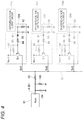
- FIG. 4 shows the connection relation between the abnormal discharge detection circuits 72 and the ASIC 61 .
- the charging-voltage output circuit 71 C corresponding to cyan is omitted.
- each of the four abnormal discharge detection circuits 72 is connected to a common signal line SL which is a shared signal line.
- the collector of the transistor Tr 1 of each abnormal discharge detection circuit 72 is connected to a port A/D 1 of the ASIC 61 via the common signal line SL. Therefore, although the charging-voltage generating circuits 70 are provided corresponding to the individual colors, the charging-voltage generating circuits 70 (the abnormal discharge detection circuits 72 ) output abnormal discharge detection signals Sv 1 to Sv 4 to a common signal path.
- the ASIC 61 of the present illustrative embodiment is configured to have the port A/D 1 (an example of a common input port) connected to the four abnormal discharge detection circuits 72 such that the abnormal discharge detection signals Sv 1 to Sv 4 output from the individual abnormal discharge detection circuits 72 are input to the ASIC 61 through the port A/D 1 .
- each of the abnormal discharge detection circuits 72 is connected to a corresponding one of the charging-voltage output circuits 71 K to 71 C (examples of the charge output circuits), that is different between the abnormal discharge detection circuits 72 . That is, the charging-voltage output circuits 71 , which are connected to the different corresponding abnormal discharge detection circuit 72 , are different from each other.
- the port A/D 1 an example of a common input port
- each of the abnormal discharge detection circuits 72 is connected to a corresponding one of the charging-voltage output circuits 71 K to 71 C (examples of the charge output circuits), that is different between the abnormal discharge detection circuits
- the abnormal discharge detection circuit 72 K is connected to the charging-voltage output circuit 71 K
- the abnormal discharge detection circuit 72 Y is connected to the charging-voltage output circuit 71 Y
- the abnormal discharge detection circuit 72 M is connected to the charging-voltage output circuit 71 M.
- the charging-voltage output circuits 71 K, 71 Y, 71 M are different from each other.
- a detection resistor 101 for detecting the abnormal discharge detection signals Sv is connected.
- a resistor 103 and a capacitor 104 are connected to a terminal of the detection resistor 101 close to the ASIC 61 .
- One end of each of the resistor 103 and the capacitor 104 is connected to the detection resistor 101 (the port A/D 1 of the ASIC 61 ), and the other end is connected to the ground.
- the resistor 103 and the capacitor 104 smooth each abnormal discharge detection signal Sv detected by the detection resistor 101 .
- the transistors Tr 1 are in an OFF state. Therefore, any abnormal discharge detection signal Sv is not output from the collectors of the transistors Tr 1 .
- a corresponding transistor Tr 1 is turned on. Therefore, an abnormal discharge detection signal Sv is input from the corresponding transistor Tr 1 to the ASIC 61 .
- the ASIC 61 can detect whether abnormal discharge has occurred.
- the ASIC 61 performs a predetermined process such as a process of notifying a user that abnormal discharge has occurred and urging the user to clean the charging wires.
- the ON/OFF characteristic of the transistor Tr 1 of each abnormal discharge detection circuit 72 i.e. the characteristic (sensitivity) for discharging the abnormal discharge detection signals Sv according to the level of abnormal discharge (the magnitude of an abnormal discharge current) can be changed by changing circuit constants and the like of the corresponding abnormal discharge detection circuit 72 .
- the zener diode 91 may be replaced with another one having a different zener voltage (breakdown voltage).
- the resistors 94 and 95 and the capacitor 96 may be replaced with others having different resistance values and a different electrostatic capacitance value.
- the transistor Tr 1 may be replaced with another one having a different I-V characteristic.
- the connection path between the detection resistor 92 of an abnormal discharge detection circuit 72 and a corresponding corona charger 41 via the ground is long, and thus attenuation of an abnormal discharge current in the path from the corona charger 41 to the detection resistor 92 is significant, it is required to make the sensitivity of the corresponding abnormal discharge detection circuit higher than those of the other abnormal discharge detection circuits 72 .
- the absolute value of the zener voltage (breakdown voltage) of the zener diode 91 is decreased and the transistor Tr 1 is configured to be more likely to be turned on (to be turned on by an abnormal discharge current having a smaller current value), such that the sensitivity increases.
- the absolute value of the zener voltage of the zener diode 91 is increased and the transistor Tr 1 is configured to be more unlikely to be turned on (to be turned on by an abnormal discharge current having a larger current value), such that the sensitivity decreases.
- the sensitivities of the individual abnormal discharge detection circuits 72 as described above, it is possible to equalize the sensitivities for abnormal discharge and improve the detection accuracy.
- adjusting high sensitivity of an abnormal discharge detection circuit 72 to lower sensitivity decreases the sensitivity of the whole device. For this reason, it is preferable that sensitivity adjustment be performed on abnormal discharge detection circuits 72 having low sensitivities, thereby increasing the sensitivities.
- the four abnormal discharge detection circuits 72 of the present illustrative embodiment are formed in the same circuit configuration. While forming the abnormal discharge detection circuits 72 in the same circuit configuration, it is possible to adjust their sensitivities by changing circuit constants and the like. Therefore, it is possible to individually change the sensitivity of each abnormal discharge detection circuit 72 while reducing the manufacturing cost.
- the printer 1 is an example of the image forming apparatus.
- the ASIC 61 is an example of the controller.
- the charging-voltage output circuits 71 are examples of the charge output circuits.
- the port A/D 1 is an example of the common input port.
- the wire voltages CHG are examples of the charging voltage.
- the printer 1 (the image forming apparatus) of the first illustrative embodiment includes the photosensitive member 31 , the plurality of corona chargers 41 configured to charge the photosensitive member 31 by corona discharge, the plurality of charging-voltage output circuits 71 (the charge output circuits) configured to output the wire voltage CHG (the charging voltage) being applied to each of the corona chargers 41 , the plurality of abnormal discharge detection circuits 72 configured to output the abnormal discharge detection signal Sv according to abnormal discharge occurring in each of the corona chargers 41 , and the ASIC 61 (the controller) configured to have the port A/D 1 (the common input port) connected to the abnormal discharge detection circuits 72 wherein the abnormal discharge detection signal Sv output from each of the abnormal discharge detection circuits 72 is input to the ASIC 61 through the port A/D 1 .
- Each of the abnormal discharge detection circuits 72 is connected to a corresponding one circuit out of the charging-voltage output circuits 71 , which is different from the abnormal discharge detection circuits 72 .
- the abnormal discharge detection circuits 72 configured to output the abnormal discharge detection signals Sv according to abnormal discharge occurring in the corona chargers 41 are connected to the charging-voltage output circuits 71 (the charge output circuits), respectively.
- the ASIC 61 has the port A/D 1 (the common input port) connected to the abnormal discharge detection circuits 72 such that the abnormal discharge detection signals Sv 1 to Sv 4 are input from the individual abnormal discharge detection circuits 72 to the port A/D 1 . Therefore, it is possible to reduce the number of input ports required for the ASIC 61 to receive the abnormal discharge detection signals Sv 1 to Sv 4 .
- each abnormal discharge detection circuit 72 is connected to the individual charging-voltage output circuits 71 , respectively, it is possible to change circuit constants and the like of each abnormal discharge detection circuit 72 to other values. Therefore, it is possible to optimize conditions for outputting the abnormal discharge detection signals Sv, i.e. the sensitivities for detecting abnormal discharge, according to the characteristics of abnormal discharge occurring in the individual corona chargers 41 , the connection configurations, and so on. As a result, it is possible to accurately detect abnormal discharge while reducing the number of input ports required for the ASIC 61 to receive the abnormal discharge detection signals Sv 1 to Sv 4 .
- Each of the corona chargers 41 includes a charging wire 42 , and a grid 43 disposed between the photosensitive member 31 and the charging wire 42 .
- At least one of the charging-voltage output circuits 71 (the charge output circuits) is connected to a charging wire 42 provided in each of the corona chargers 41 , and applies a wire voltage CHG (a charging voltage) to the charging wire 42 .
- the charge output circuits for example, the grid voltage adjustment circuits 81
- the abnormal discharge detection circuits 72 are connected to the grids 43 (see FIG. 6 )
- the possibility that abnormal discharge currents do not flow in the grids 43 and it is impossible to detect abnormal discharge increases.
- the charging-voltage output circuits 71 (the charge output circuits) are connected to the charging wires 42
- the abnormal discharge detection circuits 72 are connected to the charging wires 42 (the first illustrative embodiment)
- even though any abnormal discharge current does not flow on the side close to the grids 43 for example, when an abnormal discharge detection circuit flows on the side close to the charging wires 42 and returns to an abnormal discharge detection circuit 72 via the ground, it becomes possible to detect abnormal discharge. Therefore, according to the configuration in which the abnormal discharge detection circuits 72 are provided close to the charging wires 42 , it becomes possible to further improve the accuracy of detection of abnormal discharge as compared to the configuration in which the abnormal discharge detection circuits 72 are provided close to the grid 43 .
- one corona charger 41 is connected to one charging-voltage output circuit 71 such that a wire voltage CHG is supplied to the corona charger.
- a plurality of corona chargers 41 are connected to one charging-voltage output circuit 71 . For example, as shown in FIG.
- the ASIC 61 can perform printing by driving only circuits and other components corresponding to black (the charging-voltage generating circuit 70 K and the photosensitive member 31 K). Since the number of circuits and other components which need to be driven decreases, it is possible to suppress power consumption and suppress wearing of the printer.
- the ASIC 61 drives, for example, all of the charging-voltage generating circuits 70 and the photosensitive members 31 , thereby performing printing.
- the ASIC 61 adjusts the wire voltage CHG 2 by controlling the charging-voltage output circuit 71 Y, for example, on the basis of a grid current Ig of three grid currents Ir 2 to Ir 4 having the smallest current value.
- a grid current Ig of three grid currents Ir 2 to Ir 4 having the smallest current value.
- the ASIC controls the wire voltage CHG 2 .
- the corona chargers 41 Y, 41 M, and 41 C is connected to one charging-voltage output circuit 71 Y so as to share the charging-voltage output circuit 71 Y
- the load of a path for outputting the wire voltage CHG 2 of the charging-voltage output circuit 71 Y increases.
- the charging-voltage output circuit 71 Y becomes a high-load output circuit having an output path having a higher load as compared to the charging-voltage output circuit 71 K.
- the charging-voltage output circuit 71 K becomes a low-load output circuit having an output path having a lower load as compared to the charging-voltage output circuit 71 Y.
- the charging-voltage output circuit 71 Y which is a high-load output circuit needs to apply a desired wire voltage CHG 2 in response to an increase in the load, and needs to increase the output (power), for example, such that power is sufficient.
- the charging-voltage output circuit 71 Y of the second illustrative embodiment becomes a high-power charge output circuit having a larger output as compared to the charging-voltage output circuit 71 K.
- the corona charger 41 K and the corona chargers 41 Y, 41 M, and 41 C become different from each other in the aspect of abnormal discharge (such as the current value of an abnormal discharge current). Therefore, when one abnormal discharge detection circuit 72 is connected to the charging-voltage output circuits 71 K and 71 Y having different outputs, it may be impossible to accurately detect abnormal discharge occurring in each corona charger 41 .
- the sensitivity of the abnormal discharge detection circuit 72 K connected to the low-power charging-voltage output circuit 71 K it can be considered to increase the sensitivity of the abnormal discharge detection circuit 72 K connected to the low-power charging-voltage output circuit 71 K.
- the sensitivity of only one of the abnormal discharge detection circuits 72 K and 72 Y may be adjusted.
- three corona chargers 41 Y, 41 M, and 41 C are connected to one charging-voltage output circuit 71 Y; however, two, or four, or more corona chargers 41 may be connected.
- the charging-voltage output circuit 71 Y is an example of a high-load output circuit.
- the charging-voltage output circuit 71 K is an example of a low-load output circuit.
- the charging-voltage output circuits 71 (the charge output circuits) includes the charging-voltage output circuit 71 Y (the high-load output circuit), and the charging-voltage output circuit 71 K (the low-load output circuit) having a lower load of a path for outputting the wire voltage CHG (a charging voltage) than a load of a path of the charging-voltage output circuit 71 Y for outputting the wire voltage CHG.
- the sensitivity of detecting the abnormal-discharge by the abnormal discharge detection circuit 72 Y connected to the charging-voltage output circuit 71 Y is lower than sensitivity of detecting the abnormal-discharge by the abnormal discharge detection circuit 72 K connected to the charging-voltage output circuit 71 K.
- the load of the path of the charging-voltage output circuit 71 Y (the high-load output circuit) for outputting the wire voltage CHG 2 (a charging voltage) is high, and the output of the charging-voltage output circuit 71 Y (the high-load output circuit) is higher than that of the charging-voltage output circuit 71 K (the low-load output circuit).
- the load of an output path increases as the number of the corona chargers 41 which are connected by the output path increases, or as the length of the connection path between a corresponding charging-voltage output circuit 71 (a charge output circuit) and a corresponding corona charger 41 increases.
- the sensitivity of the abnormal discharge detection circuit 72 Y connected to the charging-voltage output circuit 71 Y decreases as the output increases.
- the sensitivity of the abnormal discharge detection circuit 72 K connected to the charging-voltage output circuit 71 K increases as the output decreases. According to this configuration, it is possible to adjust the sensitivities according to the difference between the output capacities of the charging-voltage output circuits 71 K and 71 Y, and it is possible to accurately detect abnormal discharge.
- the abnormal discharge detection circuit 72 Y connected to the charging-voltage output circuit 71 Y (the high-load output circuit) and the abnormal discharge detection circuit 72 K connected to the charging-voltage output circuit 71 K (the low-load output circuit) have the same circuit configuration.
- the circuit constants of the abnormal discharge detection circuits 72 K and 72 Y are set such that the sensitivity of the abnormal discharge detection circuit 72 Y connected to the charging-voltage output circuit 71 Y is lower than the sensitivity of the abnormal discharge detection circuit 72 K connected to the charging-voltage output circuit 71 K.
- the resistors 94 and 95 and the capacitor 96 of the abnormal discharge detection circuit 72 K are changed, such that the transistor Tr 1 is turned on by an abnormal discharge current having a smaller current value and the sensitivity for detecting abnormal discharge increases.
- the circuit configurations of the abnormal discharge detection circuits 72 K and 72 Y are standardized, it is possible to adjust the sensitivities of the charging-voltage output circuits 71 K and 71 Y according to the difference between their output capacities by changing the circuit constants while reducing the manufacturing cost.
- the number of the corona chargers 41 connected to the charging-voltage output circuit 71 Y (the high-load output circuit) (in the present illustrative embodiment, three) is larger than the number of the corona chargers 41 connected to the charging-voltage output circuit 71 K (the low-load output circuit) (in the present illustrative embodiment, one).
- the charging-voltage output circuit 71 Y (the high-load output circuit) is configured to be connected to more corona chargers 41 and have a higher output as compared to the charging-voltage output circuit 71 K (the low-load output circuit).
- the sensitivities according to the difference between the output capacities of the charging-voltage output circuits 71 K and 71 Y as described above, it is possible to adjust the difference between the sensitivities.
- Each of the corona chargers 41 includes a charging wire 42 , and a grid 43 disposed between the corresponding photosensitive member 3 land the charging wire 42 .
- the charging-voltage output circuit 71 Y (the high-load output circuit) is connected to the charging wires 42 Y, 42 M, and 42 C provided in the corona chargers 41 Y, 41 M, and 41 C, and applies the wire voltage CHG 2 (a charging voltage) to the charging wires 42 Y, 42 M, and 42 C.
- the charging-voltage output circuits (the charging-voltage output circuits 71 ) configured to apply the wire voltages CHG (charging voltages) to the charging wires 42 are required to have charging voltages having larger voltage values as compared to the charge output circuits (the grid voltage adjustment circuits 81 ) configured to apply the grid voltages GRID (charging voltages) to the grids 43 .
- the wire voltage CHG 2 (a charging voltage) is applied from the high-load output circuit (the charging-voltage output circuit 71 Y) to the charging wires 42 Y, 42 M, and 42 C
- the output difference between the charging-voltage output circuit 71 Y (the high-load output circuit) and the charging-voltage output circuit 71 K (the low-load output circuit) increases.
- the wire voltage CHG 2 (a charging voltage) is applied from the high-load output circuit (the charging-voltage output circuit 71 Y) to the charging wires 42 Y, 42 M, and 42 C, it is very effective to adjust the sensitivities by changing the circuit constants and the like of the abnormal discharge detection circuits 72 K and 72 Y.
- the charging-voltage output circuit 71 K (the low-load output circuit) configured to apply the wire voltage CHG 1 to the corona charger 41 K (the charging wire 42 K) of black
- the charging-voltage output circuit 71 Y (the high-load output circuit) connected to the corona chargers 41 Y, 41 M, and 41 C (the charging wires 42 Y, 42 M, and 42 C) of the other colors (yellow, magenta, and cyan) such that the corona chargers are connected in parallel and configured to apply the wire voltage CHG 2 are separate circuits.
- the voltage values of the DC power supplies Vcc 1 of the individual abnormal discharge detection circuits 72 shown in FIG. 4 are set to different values.
- all of the voltages of the DC power supplies Vcc 1 of the abnormal discharge detection circuits 72 are standardized with 5.0 V.
- the voltage value of the DC power supply Vcc 1 of the abnormal discharge detection circuit 72 K corresponding to black is set to 6.5 V.
- the voltage value of the DC power supply Vcc 1 of the abnormal discharge detection circuit 72 Y corresponding to yellow is set to 5.0 V.
- the voltage value of the DC power supply Vcc 1 of the abnormal discharge detection circuit 72 M corresponding to magenta is set to 3.3 V.
- the voltage value of the DC power supply Vcc 1 of the abnormal discharge detection circuit 72 C corresponding to cyan is set to 1.7 V.
- the circuit constants of the four abnormal discharge detection circuits 72 are set to the same value.
- the abnormal discharge detection circuits 72 output abnormal discharge detection signals Sv 1 to Sv 4 having different voltage values (signal levels) according to the voltage values of the DC power supplies Vcc 1 , respectively.
- the circuit constants of the abnormal discharge detection circuits 72 may be set to different values such that the individual abnormal discharge detection circuits 72 output abnormal discharge detection signals Sv 1 to Sv 4 having different voltage values (signal levels), respectively.
- the ASIC 61 detects the signal level of each of the abnormal discharge detection signals Sv 1 to Sv 4 input from the port A/D 1 , thereby capable of specifying an abnormal discharge detection circuit 72 having output the corresponding abnormal discharge detection signal Sv, i.e. one of the corona chargers 41 K to 41 C in which abnormal discharge has occurred.
- the ASIC 61 displays a printing color for which abnormal discharge has occurred, on a display unit (not shown in the drawings) of the printer 1 . According to this configuration, when seeing the content of the display unit, the user can clean the charging wire 42 of the corona charger 41 in which abnormal discharge has occurred, thereby removing toner and paper powder, thereby capable of suppressing occurrence of abnormal discharge during the next printing.
- the printer 1 of the third illustrative embodiment includes the plurality of photosensitive members 31 .
- Each of the corona chargers 41 is provided corresponding to each of the photosensitive members 31 .
- the abnormal discharge detection circuits 72 are connected to the different power supplies (the DC power supplies Vcc 1 ), and outputs the abnormal discharge detection signals Sv 1 to Sv 4 having signal levels different from each another.
- the abnormal discharge detection circuits 72 are provided corresponding to each of the corona chargers 41 (the photosensitive members 31 ).
- the abnormal discharge detection circuits 72 are connected to the different DC power supplies Vcc 1 , and outputs the abnormal discharge detection signals Sv 1 to Sv 4 having the different signal levels (voltage values or current values) to the ASIC 61 (the controller).
- the ASIC 61 can specify a corona charger 41 in which abnormal discharge has occurred.
- the abnormal discharge detection circuits 72 are connected to the charging-voltage generating circuits 70 , and are connected to the sides of the corona chargers 41 close to the charging wires 42 .
- the charging-voltage generating circuits 70 become the charge output circuits of the present disclosure.
- the abnormal discharge detection circuits 72 are connected to the sides close to the grids 43 (the grid voltage adjustment circuits 81 ).
- the abnormal discharge detection circuit 72 M is connected to the grid voltage control circuit 81 M corresponding to magenta as shown in FIG. 6 will be described.
- the abnormal discharge detection circuit 72 M of the fourth illustrative embodiment is connected to a node ND of the grid voltage control circuit 81 M.
- the node ND is, for example, the connection point of the transistor Q 1 and the grid 43 M as shown in FIG. 2 .
- the grid 43 M outputs a current toward the node ND, according to a voltage generated during corona discharge or abnormal discharge.
- a variable resistor 121 and a detection resistor 123 are connected in series.
- the variable resistor 121 and the detection resistor 123 are for adjusting the voltage on the node ND such that the grid voltage GRID 3 generated in the grid 43 M becomes a predetermined voltage.
- the voltage on the node ND can be changed by adjusting the resistance value of the variable resistor 121 .
- the connection point of the node ND and the variable resistor 121 is connected to the transistor Tr 1 via a capacitor 125 .
- the capacitor 125 shuts off a current from the node ND to the base of the transistor Tr 1 .
- the abnormal discharge detection circuit 72 M can suppress the transistor Tr 1 from being turned on in the case where a current supplied to the node ND includes noise, thereby suppressing erroneous detection of abnormal discharge.
- the capacitor 125 flows an abnormal discharge current suddenly increasing during occurrence of abnormal discharge from the node ND toward the transistor Tr 1 .
- the capacitor 125 takes an AC component from the abnormal discharge current, and applies the AC component to the transistor Tr 1 .
- each abnormal discharge detection circuit 72 of the first illustrative embodiment the zener diode 91 is connected to the base of the transistor Tr 1 .
- the zener diode 91 is used. According to this configuration, it is possible to protect the circuits of each abnormal discharge detection circuit 72 even though a high voltage is applied after occurrence of abnormal discharge.
- each grid voltage adjustment circuit 81 only during abnormal discharge, a large current is likely to be generated. Therefore, in protecting the circuit after abnormal discharge, a zener diode 91 is not necessarily needed. For this reason, in the case of connecting an abnormal discharge detection circuit 72 to a grid voltage adjustment circuits 81 , instead of the zener diode 91 , the capacitor 125 is connected to the base of the transistor Tr 1 , whereby it is possible to reduce the manufacturing cost.
- abnormal discharge detection circuit 72 M having the above-described configuration, similarly to the abnormal discharge detection circuit 72 M of the first illustrative embodiment, when abnormal discharge occurs in a corresponding corona charger 41 , an abnormal discharge current flows in the grid 43 M, and thus the transistor Tr 1 is turned on.
- the abnormal discharge detection signal Sv 3 is input from the transistor Tr 1 of the abnormal discharge detection circuit 72 M, the ASIC 61 can detect occurrence of abnormal discharge.
- each of the corona chargers 41 includes a charging wire 42 , and a grid 43 disposed between the charging wire 42 and a corresponding photosensitive member 31 .
- At least one (the grid voltage control circuit 81 M) of the charge output circuits (the charging-voltage generating circuits 70 and the grid voltage adjustment circuits 81 ) is connected to the grids 43 provided in each of the corona chargers 41 , and applies the grid voltage GRID 3 (a charging voltage) to the grid 43 M.
- the abnormal discharge detection circuit 72 M is connected to the grid 43 , thereby capable of detecting abnormal discharge. Further, it is possible to accurately detect abnormal discharge by adjusting the sensitivity of the abnormal discharge detection circuit 72 M connected to the grid 43 M.
- the configurations of the abnormal discharge detection circuits 72 of each illustrative embodiment described above are examples, and can be appropriately changed.
- an operational amplifier OP 2 an amplifier circuit for amplifying the abnormal discharge detection signal Sv 1 may be provided.
- components identical to those of the illustrative embodiments described above are denoted by the same reference symbols, and a description thereof is appropriately omitted.
- the non-inversion input terminal of the operational amplifier OP 2 is connected to the collector of the transistor Tr 1 via a resistor 131 .
- the non-inversion input terminal of the operational amplifier OP 2 is connected to the ground via a resistor 132 .
- the output terminal of the operational amplifier OP 2 is connected to the non-inversion input terminal via resistors 135 and 136 .
- the operational amplifier OP 2 amplifies the abnormal discharge detection signal Sv 1 input to the non-inversion input terminal, and outputs the amplified signal to the ASIC 61 (see FIG. 4 ).
- an operational amplifier OP 2 it is effective to connect an operational amplifier OP 2 .
- the abnormal discharge detection circuit 72 K and the ASIC 61 are placed apart from each other according to the layout of circuits and the line length of the common signal line SL (see FIG. 4 ) for transmitting the abnormal discharge detection signal Sv 1 is long.
- the attenuation rate of an abnormal discharge detection signal Sv during transmission in the common signal line SL increases.
- the sensitivity of the abnormal discharge detection circuit 72 K may decrease.
- an operational amplifier OP 2 is connected so as to amplify the abnormal discharge detection signal Sv 1 , thereby increasing the sensitivity, it is possible to adjust the signal level of the abnormal discharge detection signal Sv 1 .
- an operational amplifier OP 2 for amplifying the abnormal discharge detection signal Sv 1 may be connected to the abnormal discharge detection circuit 72 K connected to the charging-voltage output circuit 71 K (the low-load output circuit).
- the abnormal discharge detection signal Sv 1 output from the abnormal discharge detection circuit 72 K (the low-load output circuit) is amplified, whereby it is possible to improve the sensitivity and adjust the sensitivity difference.
- a comparator 141 (an example of a comparison circuit) may be provided in the abnormal discharge detection circuit 72 K of the low-power charging-voltage output circuit 71 K, thereby adjusting the sensitivity.
- the positive terminal of the capacitor 93 the positive terminal of the detection resistor 92 , and the charging-voltage output circuit 71 K (the low-voltage-side output terminal T 2 of FIG. 3 ) are connected.
- a reference voltage obtained by dividing the voltage of the DC power supply Vcc 1 by voltage division resistors 142 and 143 is input.
- an output resistor 145 is connected to the output terminal of the comparator 141 .
- the comparator 141 compares the voltage input to the non-inversion input terminal (the voltage caused by abnormal discharge) and the reference voltage, and outputs the comparison result as the abnormal discharge detection signal Sv 1 to the ASIC 61 .
- the abnormal discharge detection circuit 72 K connected to the charging-voltage output circuit 71 K includes the comparator 141 configured to compare the voltage caused by abnormal discharge with the reference voltage and output the abnormal discharge detection signal Sv 1 .
- the comparator 141 configured to compare the voltage caused by abnormal discharge with the reference voltage and output the abnormal discharge detection signal Sv 1 .
- the operational amplifier OP 2 or the comparator 141 is connected to the low-power charging-voltage output circuit 71 K (the abnormal discharge detection circuit 72 K); however, the present disclosure is not limited thereto.
- an operational amplifier OP 2 or the like may be provided in each abnormal discharge detection circuit 72 shown in FIG. 4 .
- An operational amplifier OP 2 or the like may be provided in the high-power charging-voltage output circuit 71 Y (the abnormal discharge detection circuit 72 Y) shown in FIG. 5 .
- An operational amplifier OP 2 or the like may be provided in the grid voltage control circuit 81 M (the abnormal discharge detection circuit 72 M close to the grid 43 M) shown in FIG. 6 .
- the present disclosure is not limited thereto.
- the present disclosure can be applied to a configuration in which the plurality of corona chargers 41 corresponds to one photosensitive member 31 , for example, a printer (an image forming apparatus) for superimposing toner images of individual colors on one photosensitive member 31 and transferring them on a sheet P at once.
- the number of photosensitive members 31 may be one.
- the printer 1 may be a monochrome printer having only a photosensitive member 31 K corresponding to black.
- the high-voltage power supply circuit 62 may have a configuration having not only abnormal discharge detection circuits 72 connected on the sides close to the charging wires 42 but also abnormal discharge detection circuits 72 connected on the sides close to the grids 43 .
- the charge output circuits of the present disclosure correspond not only to the charging-voltage output circuits 71 but also to the grid voltage adjustment circuits 81 .
- abnormal discharge detection circuits 72 may be provided, respectively.
- the ASIC 61 may determine whether abnormal discharge has occurred by comparing detection results of the abnormal discharge detection circuits 72 provided on both sides, i.e. the side close to the charging wire 42 and the side close to the grid 43 .
- the drum-shaped photosensitive members 31 have been taken.
- the photosensitive members are not limited thereto, and may be, for example, belt-shaped photosensitive members.
- the scorotron type corona chargers 41 having the grids 43 are used; however, the present disclosure is not limited thereto.
- the corona chargers of the present disclosure may be corotron type corona chargers having no grids 43 .
- the controller the ASIC 61 is used as the controller.
- the controller of the present disclosure is not limited to the case where it is configured with dedicated hardware such as the ASIC 61 , and may be configured with, for example, software executable on a CPU.
- the controller may be an ASIC having a CPU mounted thereon.
- the electrophotographic laser printer 1 is used; however, the present disclosure is not limited thereto.
- the image forming apparatus of the present disclosure may be any other apparatus such as a multi-function apparatus, a facsimile machine, or a copy machine.
Landscapes
- Physics & Mathematics (AREA)
- Engineering & Computer Science (AREA)
- Plasma & Fusion (AREA)
- General Physics & Mathematics (AREA)
- Electrostatic Charge, Transfer And Separation In Electrography (AREA)
- Control Or Security For Electrophotography (AREA)
- Microelectronics & Electronic Packaging (AREA)
Abstract
Description
Claims (7)
Applications Claiming Priority (2)
| Application Number | Priority Date | Filing Date | Title |
|---|---|---|---|
| JP2017-129806 | 2017-06-30 | ||
| JP2017129806A JP6965599B2 (en) | 2017-06-30 | 2017-06-30 | Image forming device |
Publications (2)
| Publication Number | Publication Date |
|---|---|
| US20190079427A1 US20190079427A1 (en) | 2019-03-14 |
| US10691040B2 true US10691040B2 (en) | 2020-06-23 |
Family
ID=65228049
Family Applications (1)
| Application Number | Title | Priority Date | Filing Date |
|---|---|---|---|
| US15/936,523 Active US10691040B2 (en) | 2017-06-30 | 2018-03-27 | Abnormal discharge detection circuit for corona chargers |
Country Status (2)
| Country | Link |
|---|---|
| US (1) | US10691040B2 (en) |
| JP (1) | JP6965599B2 (en) |
Cited By (1)
| Publication number | Priority date | Publication date | Assignee | Title |
|---|---|---|---|---|
| US11112720B2 (en) * | 2019-07-25 | 2021-09-07 | Canon Kabushiki Kaisha | Technique for transmitting signal indicating abnormality in image forming apparatus |
Families Citing this family (1)
| Publication number | Priority date | Publication date | Assignee | Title |
|---|---|---|---|---|
| JP7216546B2 (en) * | 2018-12-26 | 2023-02-01 | キヤノン株式会社 | image forming device |
Citations (5)
| Publication number | Priority date | Publication date | Assignee | Title |
|---|---|---|---|---|
| US20070147858A1 (en) * | 2005-12-27 | 2007-06-28 | Brother Kogyo Kabushiki Kaisha | Image forming apparatus |
| US20090010661A1 (en) | 2007-07-06 | 2009-01-08 | Brother Kogyo Kabushiki Kaisha | Image Forming Apparatus |
| US20090060535A1 (en) * | 2007-08-27 | 2009-03-05 | Brother Kogyo Kabushiki Kaisha | Image forming apparatus |
| US20120051761A1 (en) * | 2010-08-31 | 2012-03-01 | Brother Kogyo Kabushiki Kaisha | Image-Forming Device |
| US20140079429A1 (en) * | 2012-09-19 | 2014-03-20 | Brother Kogyo Kabushiki Kaisha | Image forming apparatus |
Family Cites Families (7)
| Publication number | Priority date | Publication date | Assignee | Title |
|---|---|---|---|---|
| JPS59141350U (en) * | 1983-03-11 | 1984-09-21 | 株式会社リコー | Leak detection device for electrophotographic copying machines |
| JP3035914B2 (en) * | 1988-12-05 | 2000-04-24 | 富士ゼロックス株式会社 | Abnormal control device for high voltage power supply |
| JPH04109768U (en) * | 1991-03-08 | 1992-09-22 | 富士ゼロツクス株式会社 | High voltage power supply |
| JP2006010881A (en) * | 2004-06-23 | 2006-01-12 | Ricoh Co Ltd | Image forming apparatus |
| JP5573566B2 (en) * | 2010-09-30 | 2014-08-20 | ブラザー工業株式会社 | Image forming apparatus |
| JP5206811B2 (en) * | 2011-01-31 | 2013-06-12 | ブラザー工業株式会社 | Image forming apparatus |
| JP6464557B2 (en) * | 2014-02-28 | 2019-02-06 | ブラザー工業株式会社 | Image forming apparatus |
-
2017
- 2017-06-30 JP JP2017129806A patent/JP6965599B2/en active Active
-
2018
- 2018-03-27 US US15/936,523 patent/US10691040B2/en active Active
Patent Citations (9)
| Publication number | Priority date | Publication date | Assignee | Title |
|---|---|---|---|---|
| US20070147858A1 (en) * | 2005-12-27 | 2007-06-28 | Brother Kogyo Kabushiki Kaisha | Image forming apparatus |
| JP2007178595A (en) | 2005-12-27 | 2007-07-12 | Brother Ind Ltd | Image forming apparatus |
| US7620335B2 (en) | 2005-12-27 | 2009-11-17 | Brother Kogyo Kabushiki Kaisha | Image forming apparatus |
| US20090010661A1 (en) | 2007-07-06 | 2009-01-08 | Brother Kogyo Kabushiki Kaisha | Image Forming Apparatus |
| JP2009015168A (en) | 2007-07-06 | 2009-01-22 | Brother Ind Ltd | Image forming apparatus |
| US7986889B2 (en) | 2007-07-06 | 2011-07-26 | Brother Kogyo Kabushiki Kaisha | Abnormality detection in an image forming apparatus |
| US20090060535A1 (en) * | 2007-08-27 | 2009-03-05 | Brother Kogyo Kabushiki Kaisha | Image forming apparatus |
| US20120051761A1 (en) * | 2010-08-31 | 2012-03-01 | Brother Kogyo Kabushiki Kaisha | Image-Forming Device |
| US20140079429A1 (en) * | 2012-09-19 | 2014-03-20 | Brother Kogyo Kabushiki Kaisha | Image forming apparatus |
Cited By (1)
| Publication number | Priority date | Publication date | Assignee | Title |
|---|---|---|---|---|
| US11112720B2 (en) * | 2019-07-25 | 2021-09-07 | Canon Kabushiki Kaisha | Technique for transmitting signal indicating abnormality in image forming apparatus |
Also Published As
| Publication number | Publication date |
|---|---|
| JP2019012232A (en) | 2019-01-24 |
| JP6965599B2 (en) | 2021-11-10 |
| US20190079427A1 (en) | 2019-03-14 |
Similar Documents
| Publication | Publication Date | Title |
|---|---|---|
| US8019241B2 (en) | Image forming apparatus | |
| US7986889B2 (en) | Abnormality detection in an image forming apparatus | |
| US8503896B2 (en) | Image formation device and image formation method to prevent spark discharge | |
| US8594521B2 (en) | Image forming apparatus | |
| US20160238983A1 (en) | Power supply apparatus and image forming apparatus | |
| US20080226317A1 (en) | Image Forming Apparatus and Method | |
| JP2009229577A (en) | Image forming apparatus | |
| US10691040B2 (en) | Abnormal discharge detection circuit for corona chargers | |
| US20120051772A1 (en) | Image Forming Apparatus and Method for Controlling Charger | |
| US8676067B2 (en) | Image forming apparatus | |
| US8218995B2 (en) | Power supply device and image forming apparatus having the same | |
| JP4763990B2 (en) | Image forming apparatus and high-voltage power supply device used for image forming apparatus | |
| US9342030B1 (en) | Power supply apparatus for superimposing direct current voltage on alternating current voltage and outputting resulting voltage | |
| US8014174B2 (en) | Image forming apparatus | |
| JP6015015B2 (en) | Image forming apparatus | |
| US11835910B2 (en) | Power source apparatus and image forming apparatus having a control unit configured to switch a target voltage of an output voltage output from a secondary side of a transformer | |
| JP6056156B2 (en) | Image forming apparatus | |
| JP2019012231A (en) | Image forming apparatus and control method | |
| US10031436B2 (en) | High voltage generation apparatus and image forming apparatus | |
| JP2023111293A (en) | image forming device | |
| JP2023148180A (en) | Image forming device | |
| JP6379856B2 (en) | Image forming apparatus, control method, and program | |
| JP2014235229A (en) | Image forming apparatus | |
| JPH0623899B2 (en) | Image forming device | |
| JP2007052690A (en) | Power supply apparatus and image processing apparatus |
Legal Events
| Date | Code | Title | Description |
|---|---|---|---|
| FEPP | Fee payment procedure |
Free format text: ENTITY STATUS SET TO UNDISCOUNTED (ORIGINAL EVENT CODE: BIG.); ENTITY STATUS OF PATENT OWNER: LARGE ENTITY |
|
| AS | Assignment |
Owner name: BROTHER KOGYO KABUSHIKI KAISHA, JAPAN Free format text: ASSIGNMENT OF ASSIGNORS INTEREST;ASSIGNOR:KATOH, HIROKI;REEL/FRAME:045587/0533 Effective date: 20180323 |
|
| STPP | Information on status: patent application and granting procedure in general |
Free format text: NON FINAL ACTION MAILED |
|
| STPP | Information on status: patent application and granting procedure in general |
Free format text: RESPONSE TO NON-FINAL OFFICE ACTION ENTERED AND FORWARDED TO EXAMINER |
|
| STPP | Information on status: patent application and granting procedure in general |
Free format text: FINAL REJECTION MAILED |
|
| STPP | Information on status: patent application and granting procedure in general |
Free format text: DOCKETED NEW CASE - READY FOR EXAMINATION |
|
| STPP | Information on status: patent application and granting procedure in general |
Free format text: NOTICE OF ALLOWANCE MAILED -- APPLICATION RECEIVED IN OFFICE OF PUBLICATIONS |
|
| STPP | Information on status: patent application and granting procedure in general |
Free format text: AWAITING TC RESP, ISSUE FEE PAYMENT VERIFIED |
|
| STCF | Information on status: patent grant |
Free format text: PATENTED CASE |
|
| MAFP | Maintenance fee payment |
Free format text: PAYMENT OF MAINTENANCE FEE, 4TH YEAR, LARGE ENTITY (ORIGINAL EVENT CODE: M1551); ENTITY STATUS OF PATENT OWNER: LARGE ENTITY Year of fee payment: 4 |