US10679949B2 - Semiconductor package assembly with redistribution layer (RDL) trace - Google Patents
Semiconductor package assembly with redistribution layer (RDL) trace Download PDFInfo
- Publication number
- US10679949B2 US10679949B2 US15/411,077 US201715411077A US10679949B2 US 10679949 B2 US10679949 B2 US 10679949B2 US 201715411077 A US201715411077 A US 201715411077A US 10679949 B2 US10679949 B2 US 10679949B2
- Authority
- US
- United States
- Prior art keywords
- pad
- rdl
- trace
- die
- ground
- Prior art date
- Legal status (The legal status is an assumption and is not a legal conclusion. Google has not performed a legal analysis and makes no representation as to the accuracy of the status listed.)
- Active
Links
- 239000004065 semiconductor Substances 0.000 title claims abstract description 95
- 239000000758 substrate Substances 0.000 claims abstract description 83
- 150000001875 compounds Chemical class 0.000 description 9
- 238000000465 moulding Methods 0.000 description 7
- 238000005516 engineering process Methods 0.000 description 5
- 230000000712 assembly Effects 0.000 description 4
- 238000000429 assembly Methods 0.000 description 4
- 239000000853 adhesive Substances 0.000 description 3
- 230000001070 adhesive effect Effects 0.000 description 3
- 229910000679 solder Inorganic materials 0.000 description 3
- RYGMFSIKBFXOCR-UHFFFAOYSA-N Copper Chemical compound [Cu] RYGMFSIKBFXOCR-UHFFFAOYSA-N 0.000 description 2
- 239000004593 Epoxy Substances 0.000 description 2
- 239000004743 Polypropylene Substances 0.000 description 2
- 229910052802 copper Inorganic materials 0.000 description 2
- 239000010949 copper Substances 0.000 description 2
- 238000013461 design Methods 0.000 description 2
- 238000012986 modification Methods 0.000 description 2
- 230000004048 modification Effects 0.000 description 2
- 239000011368 organic material Substances 0.000 description 2
- 229920000642 polymer Polymers 0.000 description 2
- 229920001155 polypropylene Polymers 0.000 description 2
- 238000012545 processing Methods 0.000 description 2
- 229920005989 resin Polymers 0.000 description 2
- 239000011347 resin Substances 0.000 description 2
- 239000004642 Polyimide Substances 0.000 description 1
- XUIMIQQOPSSXEZ-UHFFFAOYSA-N Silicon Chemical compound [Si] XUIMIQQOPSSXEZ-UHFFFAOYSA-N 0.000 description 1
- 238000006243 chemical reaction Methods 0.000 description 1
- 238000004891 communication Methods 0.000 description 1
- 230000008878 coupling Effects 0.000 description 1
- 238000010168 coupling process Methods 0.000 description 1
- 238000005859 coupling reaction Methods 0.000 description 1
- 239000004643 cyanate ester Substances 0.000 description 1
- 239000003989 dielectric material Substances 0.000 description 1
- 239000003822 epoxy resin Substances 0.000 description 1
- 239000003365 glass fiber Substances 0.000 description 1
- 239000007788 liquid Substances 0.000 description 1
- 239000000463 material Substances 0.000 description 1
- 238000000034 method Methods 0.000 description 1
- 239000012811 non-conductive material Substances 0.000 description 1
- 229920000647 polyepoxide Polymers 0.000 description 1
- 229920001721 polyimide Polymers 0.000 description 1
- -1 polypropylene Polymers 0.000 description 1
- 229910052710 silicon Inorganic materials 0.000 description 1
- 239000010703 silicon Substances 0.000 description 1
- 239000007787 solid Substances 0.000 description 1
Images


Classifications
-
- H—ELECTRICITY
- H01—ELECTRIC ELEMENTS
- H01L—SEMICONDUCTOR DEVICES NOT COVERED BY CLASS H10
- H01L23/00—Details of semiconductor or other solid state devices
- H01L23/552—Protection against radiation, e.g. light or electromagnetic waves
-
- H—ELECTRICITY
- H01—ELECTRIC ELEMENTS
- H01L—SEMICONDUCTOR DEVICES NOT COVERED BY CLASS H10
- H01L23/00—Details of semiconductor or other solid state devices
- H01L23/48—Arrangements for conducting electric current to or from the solid state body in operation, e.g. leads, terminal arrangements ; Selection of materials therefor
- H01L23/488—Arrangements for conducting electric current to or from the solid state body in operation, e.g. leads, terminal arrangements ; Selection of materials therefor consisting of soldered or bonded constructions
- H01L23/498—Leads, i.e. metallisations or lead-frames on insulating substrates, e.g. chip carriers
- H01L23/49838—Geometry or layout
-
- H—ELECTRICITY
- H01—ELECTRIC ELEMENTS
- H01L—SEMICONDUCTOR DEVICES NOT COVERED BY CLASS H10
- H01L23/00—Details of semiconductor or other solid state devices
- H01L23/52—Arrangements for conducting electric current within the device in operation from one component to another, i.e. interconnections, e.g. wires, lead frames
- H01L23/522—Arrangements for conducting electric current within the device in operation from one component to another, i.e. interconnections, e.g. wires, lead frames including external interconnections consisting of a multilayer structure of conductive and insulating layers inseparably formed on the semiconductor body
- H01L23/528—Geometry or layout of the interconnection structure
- H01L23/5286—Arrangements of power or ground buses
-
- H—ELECTRICITY
- H01—ELECTRIC ELEMENTS
- H01L—SEMICONDUCTOR DEVICES NOT COVERED BY CLASS H10
- H01L24/00—Arrangements for connecting or disconnecting semiconductor or solid-state bodies; Methods or apparatus related thereto
- H01L24/01—Means for bonding being attached to, or being formed on, the surface to be connected, e.g. chip-to-package, die-attach, "first-level" interconnects; Manufacturing methods related thereto
- H01L24/10—Bump connectors ; Manufacturing methods related thereto
- H01L24/15—Structure, shape, material or disposition of the bump connectors after the connecting process
- H01L24/16—Structure, shape, material or disposition of the bump connectors after the connecting process of an individual bump connector
-
- H—ELECTRICITY
- H01—ELECTRIC ELEMENTS
- H01L—SEMICONDUCTOR DEVICES NOT COVERED BY CLASS H10
- H01L25/00—Assemblies consisting of a plurality of individual semiconductor or other solid state devices ; Multistep manufacturing processes thereof
- H01L25/03—Assemblies consisting of a plurality of individual semiconductor or other solid state devices ; Multistep manufacturing processes thereof all the devices being of a type provided for in the same subgroup of groups H01L27/00 - H01L33/00, or in a single subclass of H10K, H10N, e.g. assemblies of rectifier diodes
- H01L25/04—Assemblies consisting of a plurality of individual semiconductor or other solid state devices ; Multistep manufacturing processes thereof all the devices being of a type provided for in the same subgroup of groups H01L27/00 - H01L33/00, or in a single subclass of H10K, H10N, e.g. assemblies of rectifier diodes the devices not having separate containers
- H01L25/065—Assemblies consisting of a plurality of individual semiconductor or other solid state devices ; Multistep manufacturing processes thereof all the devices being of a type provided for in the same subgroup of groups H01L27/00 - H01L33/00, or in a single subclass of H10K, H10N, e.g. assemblies of rectifier diodes the devices not having separate containers the devices being of a type provided for in group H01L27/00
- H01L25/0655—Assemblies consisting of a plurality of individual semiconductor or other solid state devices ; Multistep manufacturing processes thereof all the devices being of a type provided for in the same subgroup of groups H01L27/00 - H01L33/00, or in a single subclass of H10K, H10N, e.g. assemblies of rectifier diodes the devices not having separate containers the devices being of a type provided for in group H01L27/00 the devices being arranged next to each other
-
- H—ELECTRICITY
- H01—ELECTRIC ELEMENTS
- H01L—SEMICONDUCTOR DEVICES NOT COVERED BY CLASS H10
- H01L25/00—Assemblies consisting of a plurality of individual semiconductor or other solid state devices ; Multistep manufacturing processes thereof
- H01L25/03—Assemblies consisting of a plurality of individual semiconductor or other solid state devices ; Multistep manufacturing processes thereof all the devices being of a type provided for in the same subgroup of groups H01L27/00 - H01L33/00, or in a single subclass of H10K, H10N, e.g. assemblies of rectifier diodes
- H01L25/04—Assemblies consisting of a plurality of individual semiconductor or other solid state devices ; Multistep manufacturing processes thereof all the devices being of a type provided for in the same subgroup of groups H01L27/00 - H01L33/00, or in a single subclass of H10K, H10N, e.g. assemblies of rectifier diodes the devices not having separate containers
- H01L25/065—Assemblies consisting of a plurality of individual semiconductor or other solid state devices ; Multistep manufacturing processes thereof all the devices being of a type provided for in the same subgroup of groups H01L27/00 - H01L33/00, or in a single subclass of H10K, H10N, e.g. assemblies of rectifier diodes the devices not having separate containers the devices being of a type provided for in group H01L27/00
- H01L25/0657—Stacked arrangements of devices
-
- H—ELECTRICITY
- H01—ELECTRIC ELEMENTS
- H01L—SEMICONDUCTOR DEVICES NOT COVERED BY CLASS H10
- H01L25/00—Assemblies consisting of a plurality of individual semiconductor or other solid state devices ; Multistep manufacturing processes thereof
- H01L25/18—Assemblies consisting of a plurality of individual semiconductor or other solid state devices ; Multistep manufacturing processes thereof the devices being of types provided for in two or more different subgroups of the same main group of groups H01L27/00 - H01L33/00, or in a single subclass of H10K, H10N
-
- H—ELECTRICITY
- H01—ELECTRIC ELEMENTS
- H01L—SEMICONDUCTOR DEVICES NOT COVERED BY CLASS H10
- H01L2224/00—Indexing scheme for arrangements for connecting or disconnecting semiconductor or solid-state bodies and methods related thereto as covered by H01L24/00
- H01L2224/01—Means for bonding being attached to, or being formed on, the surface to be connected, e.g. chip-to-package, die-attach, "first-level" interconnects; Manufacturing methods related thereto
- H01L2224/02—Bonding areas; Manufacturing methods related thereto
- H01L2224/023—Redistribution layers [RDL] for bonding areas
- H01L2224/0237—Disposition of the redistribution layers
- H01L2224/02375—Top view
-
- H—ELECTRICITY
- H01—ELECTRIC ELEMENTS
- H01L—SEMICONDUCTOR DEVICES NOT COVERED BY CLASS H10
- H01L2224/00—Indexing scheme for arrangements for connecting or disconnecting semiconductor or solid-state bodies and methods related thereto as covered by H01L24/00
- H01L2224/01—Means for bonding being attached to, or being formed on, the surface to be connected, e.g. chip-to-package, die-attach, "first-level" interconnects; Manufacturing methods related thereto
- H01L2224/02—Bonding areas; Manufacturing methods related thereto
- H01L2224/04—Structure, shape, material or disposition of the bonding areas prior to the connecting process
- H01L2224/0401—Bonding areas specifically adapted for bump connectors, e.g. under bump metallisation [UBM]
-
- H—ELECTRICITY
- H01—ELECTRIC ELEMENTS
- H01L—SEMICONDUCTOR DEVICES NOT COVERED BY CLASS H10
- H01L2224/00—Indexing scheme for arrangements for connecting or disconnecting semiconductor or solid-state bodies and methods related thereto as covered by H01L24/00
- H01L2224/01—Means for bonding being attached to, or being formed on, the surface to be connected, e.g. chip-to-package, die-attach, "first-level" interconnects; Manufacturing methods related thereto
- H01L2224/02—Bonding areas; Manufacturing methods related thereto
- H01L2224/04—Structure, shape, material or disposition of the bonding areas prior to the connecting process
- H01L2224/04042—Bonding areas specifically adapted for wire connectors, e.g. wirebond pads
-
- H—ELECTRICITY
- H01—ELECTRIC ELEMENTS
- H01L—SEMICONDUCTOR DEVICES NOT COVERED BY CLASS H10
- H01L2224/00—Indexing scheme for arrangements for connecting or disconnecting semiconductor or solid-state bodies and methods related thereto as covered by H01L24/00
- H01L2224/01—Means for bonding being attached to, or being formed on, the surface to be connected, e.g. chip-to-package, die-attach, "first-level" interconnects; Manufacturing methods related thereto
- H01L2224/02—Bonding areas; Manufacturing methods related thereto
- H01L2224/04—Structure, shape, material or disposition of the bonding areas prior to the connecting process
- H01L2224/05—Structure, shape, material or disposition of the bonding areas prior to the connecting process of an individual bonding area
- H01L2224/05001—Internal layers
- H01L2224/05005—Structure
- H01L2224/05008—Bonding area integrally formed with a redistribution layer on the semiconductor or solid-state body, e.g.
-
- H—ELECTRICITY
- H01—ELECTRIC ELEMENTS
- H01L—SEMICONDUCTOR DEVICES NOT COVERED BY CLASS H10
- H01L2224/00—Indexing scheme for arrangements for connecting or disconnecting semiconductor or solid-state bodies and methods related thereto as covered by H01L24/00
- H01L2224/01—Means for bonding being attached to, or being formed on, the surface to be connected, e.g. chip-to-package, die-attach, "first-level" interconnects; Manufacturing methods related thereto
- H01L2224/02—Bonding areas; Manufacturing methods related thereto
- H01L2224/04—Structure, shape, material or disposition of the bonding areas prior to the connecting process
- H01L2224/05—Structure, shape, material or disposition of the bonding areas prior to the connecting process of an individual bonding area
- H01L2224/0554—External layer
- H01L2224/05541—Structure
- H01L2224/05548—Bonding area integrally formed with a redistribution layer on the semiconductor or solid-state body
-
- H—ELECTRICITY
- H01—ELECTRIC ELEMENTS
- H01L—SEMICONDUCTOR DEVICES NOT COVERED BY CLASS H10
- H01L2224/00—Indexing scheme for arrangements for connecting or disconnecting semiconductor or solid-state bodies and methods related thereto as covered by H01L24/00
- H01L2224/01—Means for bonding being attached to, or being formed on, the surface to be connected, e.g. chip-to-package, die-attach, "first-level" interconnects; Manufacturing methods related thereto
- H01L2224/02—Bonding areas; Manufacturing methods related thereto
- H01L2224/04—Structure, shape, material or disposition of the bonding areas prior to the connecting process
- H01L2224/05—Structure, shape, material or disposition of the bonding areas prior to the connecting process of an individual bonding area
- H01L2224/0554—External layer
- H01L2224/0555—Shape
- H01L2224/05552—Shape in top view
- H01L2224/05554—Shape in top view being square
-
- H—ELECTRICITY
- H01—ELECTRIC ELEMENTS
- H01L—SEMICONDUCTOR DEVICES NOT COVERED BY CLASS H10
- H01L2224/00—Indexing scheme for arrangements for connecting or disconnecting semiconductor or solid-state bodies and methods related thereto as covered by H01L24/00
- H01L2224/01—Means for bonding being attached to, or being formed on, the surface to be connected, e.g. chip-to-package, die-attach, "first-level" interconnects; Manufacturing methods related thereto
- H01L2224/02—Bonding areas; Manufacturing methods related thereto
- H01L2224/04—Structure, shape, material or disposition of the bonding areas prior to the connecting process
- H01L2224/05—Structure, shape, material or disposition of the bonding areas prior to the connecting process of an individual bonding area
- H01L2224/0554—External layer
- H01L2224/0556—Disposition
- H01L2224/05569—Disposition the external layer being disposed on a redistribution layer on the semiconductor or solid-state body
-
- H—ELECTRICITY
- H01—ELECTRIC ELEMENTS
- H01L—SEMICONDUCTOR DEVICES NOT COVERED BY CLASS H10
- H01L2224/00—Indexing scheme for arrangements for connecting or disconnecting semiconductor or solid-state bodies and methods related thereto as covered by H01L24/00
- H01L2224/01—Means for bonding being attached to, or being formed on, the surface to be connected, e.g. chip-to-package, die-attach, "first-level" interconnects; Manufacturing methods related thereto
- H01L2224/02—Bonding areas; Manufacturing methods related thereto
- H01L2224/04—Structure, shape, material or disposition of the bonding areas prior to the connecting process
- H01L2224/06—Structure, shape, material or disposition of the bonding areas prior to the connecting process of a plurality of bonding areas
- H01L2224/0601—Structure
- H01L2224/0603—Bonding areas having different sizes, e.g. different heights or widths
-
- H—ELECTRICITY
- H01—ELECTRIC ELEMENTS
- H01L—SEMICONDUCTOR DEVICES NOT COVERED BY CLASS H10
- H01L2224/00—Indexing scheme for arrangements for connecting or disconnecting semiconductor or solid-state bodies and methods related thereto as covered by H01L24/00
- H01L2224/01—Means for bonding being attached to, or being formed on, the surface to be connected, e.g. chip-to-package, die-attach, "first-level" interconnects; Manufacturing methods related thereto
- H01L2224/02—Bonding areas; Manufacturing methods related thereto
- H01L2224/04—Structure, shape, material or disposition of the bonding areas prior to the connecting process
- H01L2224/06—Structure, shape, material or disposition of the bonding areas prior to the connecting process of a plurality of bonding areas
- H01L2224/0605—Shape
- H01L2224/06051—Bonding areas having different shapes
-
- H—ELECTRICITY
- H01—ELECTRIC ELEMENTS
- H01L—SEMICONDUCTOR DEVICES NOT COVERED BY CLASS H10
- H01L2224/00—Indexing scheme for arrangements for connecting or disconnecting semiconductor or solid-state bodies and methods related thereto as covered by H01L24/00
- H01L2224/01—Means for bonding being attached to, or being formed on, the surface to be connected, e.g. chip-to-package, die-attach, "first-level" interconnects; Manufacturing methods related thereto
- H01L2224/02—Bonding areas; Manufacturing methods related thereto
- H01L2224/04—Structure, shape, material or disposition of the bonding areas prior to the connecting process
- H01L2224/06—Structure, shape, material or disposition of the bonding areas prior to the connecting process of a plurality of bonding areas
- H01L2224/061—Disposition
- H01L2224/06102—Disposition the bonding areas being at different heights
-
- H—ELECTRICITY
- H01—ELECTRIC ELEMENTS
- H01L—SEMICONDUCTOR DEVICES NOT COVERED BY CLASS H10
- H01L2224/00—Indexing scheme for arrangements for connecting or disconnecting semiconductor or solid-state bodies and methods related thereto as covered by H01L24/00
- H01L2224/01—Means for bonding being attached to, or being formed on, the surface to be connected, e.g. chip-to-package, die-attach, "first-level" interconnects; Manufacturing methods related thereto
- H01L2224/10—Bump connectors; Manufacturing methods related thereto
- H01L2224/12—Structure, shape, material or disposition of the bump connectors prior to the connecting process
- H01L2224/13—Structure, shape, material or disposition of the bump connectors prior to the connecting process of an individual bump connector
- H01L2224/13001—Core members of the bump connector
- H01L2224/13099—Material
- H01L2224/131—Material with a principal constituent of the material being a metal or a metalloid, e.g. boron [B], silicon [Si], germanium [Ge], arsenic [As], antimony [Sb], tellurium [Te] and polonium [Po], and alloys thereof
- H01L2224/13138—Material with a principal constituent of the material being a metal or a metalloid, e.g. boron [B], silicon [Si], germanium [Ge], arsenic [As], antimony [Sb], tellurium [Te] and polonium [Po], and alloys thereof the principal constituent melting at a temperature of greater than or equal to 950°C and less than 1550°C
- H01L2224/13147—Copper [Cu] as principal constituent
-
- H—ELECTRICITY
- H01—ELECTRIC ELEMENTS
- H01L—SEMICONDUCTOR DEVICES NOT COVERED BY CLASS H10
- H01L2224/00—Indexing scheme for arrangements for connecting or disconnecting semiconductor or solid-state bodies and methods related thereto as covered by H01L24/00
- H01L2224/01—Means for bonding being attached to, or being formed on, the surface to be connected, e.g. chip-to-package, die-attach, "first-level" interconnects; Manufacturing methods related thereto
- H01L2224/10—Bump connectors; Manufacturing methods related thereto
- H01L2224/15—Structure, shape, material or disposition of the bump connectors after the connecting process
- H01L2224/16—Structure, shape, material or disposition of the bump connectors after the connecting process of an individual bump connector
- H01L2224/161—Disposition
- H01L2224/16151—Disposition the bump connector connecting between a semiconductor or solid-state body and an item not being a semiconductor or solid-state body, e.g. chip-to-substrate, chip-to-passive
- H01L2224/16221—Disposition the bump connector connecting between a semiconductor or solid-state body and an item not being a semiconductor or solid-state body, e.g. chip-to-substrate, chip-to-passive the body and the item being stacked
- H01L2224/16225—Disposition the bump connector connecting between a semiconductor or solid-state body and an item not being a semiconductor or solid-state body, e.g. chip-to-substrate, chip-to-passive the body and the item being stacked the item being non-metallic, e.g. insulating substrate with or without metallisation
- H01L2224/16227—Disposition the bump connector connecting between a semiconductor or solid-state body and an item not being a semiconductor or solid-state body, e.g. chip-to-substrate, chip-to-passive the body and the item being stacked the item being non-metallic, e.g. insulating substrate with or without metallisation the bump connector connecting to a bond pad of the item
-
- H—ELECTRICITY
- H01—ELECTRIC ELEMENTS
- H01L—SEMICONDUCTOR DEVICES NOT COVERED BY CLASS H10
- H01L2224/00—Indexing scheme for arrangements for connecting or disconnecting semiconductor or solid-state bodies and methods related thereto as covered by H01L24/00
- H01L2224/01—Means for bonding being attached to, or being formed on, the surface to be connected, e.g. chip-to-package, die-attach, "first-level" interconnects; Manufacturing methods related thereto
- H01L2224/26—Layer connectors, e.g. plate connectors, solder or adhesive layers; Manufacturing methods related thereto
- H01L2224/31—Structure, shape, material or disposition of the layer connectors after the connecting process
- H01L2224/32—Structure, shape, material or disposition of the layer connectors after the connecting process of an individual layer connector
- H01L2224/321—Disposition
- H01L2224/32135—Disposition the layer connector connecting between different semiconductor or solid-state bodies, i.e. chip-to-chip
- H01L2224/32145—Disposition the layer connector connecting between different semiconductor or solid-state bodies, i.e. chip-to-chip the bodies being stacked
-
- H—ELECTRICITY
- H01—ELECTRIC ELEMENTS
- H01L—SEMICONDUCTOR DEVICES NOT COVERED BY CLASS H10
- H01L2224/00—Indexing scheme for arrangements for connecting or disconnecting semiconductor or solid-state bodies and methods related thereto as covered by H01L24/00
- H01L2224/01—Means for bonding being attached to, or being formed on, the surface to be connected, e.g. chip-to-package, die-attach, "first-level" interconnects; Manufacturing methods related thereto
- H01L2224/26—Layer connectors, e.g. plate connectors, solder or adhesive layers; Manufacturing methods related thereto
- H01L2224/31—Structure, shape, material or disposition of the layer connectors after the connecting process
- H01L2224/32—Structure, shape, material or disposition of the layer connectors after the connecting process of an individual layer connector
- H01L2224/321—Disposition
- H01L2224/32151—Disposition the layer connector connecting between a semiconductor or solid-state body and an item not being a semiconductor or solid-state body, e.g. chip-to-substrate, chip-to-passive
- H01L2224/32221—Disposition the layer connector connecting between a semiconductor or solid-state body and an item not being a semiconductor or solid-state body, e.g. chip-to-substrate, chip-to-passive the body and the item being stacked
- H01L2224/32225—Disposition the layer connector connecting between a semiconductor or solid-state body and an item not being a semiconductor or solid-state body, e.g. chip-to-substrate, chip-to-passive the body and the item being stacked the item being non-metallic, e.g. insulating substrate with or without metallisation
-
- H—ELECTRICITY
- H01—ELECTRIC ELEMENTS
- H01L—SEMICONDUCTOR DEVICES NOT COVERED BY CLASS H10
- H01L2224/00—Indexing scheme for arrangements for connecting or disconnecting semiconductor or solid-state bodies and methods related thereto as covered by H01L24/00
- H01L2224/01—Means for bonding being attached to, or being formed on, the surface to be connected, e.g. chip-to-package, die-attach, "first-level" interconnects; Manufacturing methods related thereto
- H01L2224/42—Wire connectors; Manufacturing methods related thereto
- H01L2224/47—Structure, shape, material or disposition of the wire connectors after the connecting process
- H01L2224/48—Structure, shape, material or disposition of the wire connectors after the connecting process of an individual wire connector
- H01L2224/4805—Shape
- H01L2224/4809—Loop shape
- H01L2224/48091—Arched
-
- H—ELECTRICITY
- H01—ELECTRIC ELEMENTS
- H01L—SEMICONDUCTOR DEVICES NOT COVERED BY CLASS H10
- H01L2224/00—Indexing scheme for arrangements for connecting or disconnecting semiconductor or solid-state bodies and methods related thereto as covered by H01L24/00
- H01L2224/01—Means for bonding being attached to, or being formed on, the surface to be connected, e.g. chip-to-package, die-attach, "first-level" interconnects; Manufacturing methods related thereto
- H01L2224/42—Wire connectors; Manufacturing methods related thereto
- H01L2224/47—Structure, shape, material or disposition of the wire connectors after the connecting process
- H01L2224/48—Structure, shape, material or disposition of the wire connectors after the connecting process of an individual wire connector
- H01L2224/481—Disposition
- H01L2224/48151—Connecting between a semiconductor or solid-state body and an item not being a semiconductor or solid-state body, e.g. chip-to-substrate, chip-to-passive
- H01L2224/48221—Connecting between a semiconductor or solid-state body and an item not being a semiconductor or solid-state body, e.g. chip-to-substrate, chip-to-passive the body and the item being stacked
- H01L2224/48225—Connecting between a semiconductor or solid-state body and an item not being a semiconductor or solid-state body, e.g. chip-to-substrate, chip-to-passive the body and the item being stacked the item being non-metallic, e.g. insulating substrate with or without metallisation
- H01L2224/48227—Connecting between a semiconductor or solid-state body and an item not being a semiconductor or solid-state body, e.g. chip-to-substrate, chip-to-passive the body and the item being stacked the item being non-metallic, e.g. insulating substrate with or without metallisation connecting the wire to a bond pad of the item
- H01L2224/48229—Connecting between a semiconductor or solid-state body and an item not being a semiconductor or solid-state body, e.g. chip-to-substrate, chip-to-passive the body and the item being stacked the item being non-metallic, e.g. insulating substrate with or without metallisation connecting the wire to a bond pad of the item the bond pad protruding from the surface of the item
-
- H—ELECTRICITY
- H01—ELECTRIC ELEMENTS
- H01L—SEMICONDUCTOR DEVICES NOT COVERED BY CLASS H10
- H01L2224/00—Indexing scheme for arrangements for connecting or disconnecting semiconductor or solid-state bodies and methods related thereto as covered by H01L24/00
- H01L2224/01—Means for bonding being attached to, or being formed on, the surface to be connected, e.g. chip-to-package, die-attach, "first-level" interconnects; Manufacturing methods related thereto
- H01L2224/42—Wire connectors; Manufacturing methods related thereto
- H01L2224/47—Structure, shape, material or disposition of the wire connectors after the connecting process
- H01L2224/49—Structure, shape, material or disposition of the wire connectors after the connecting process of a plurality of wire connectors
- H01L2224/491—Disposition
- H01L2224/49105—Connecting at different heights
- H01L2224/49107—Connecting at different heights on the semiconductor or solid-state body
-
- H—ELECTRICITY
- H01—ELECTRIC ELEMENTS
- H01L—SEMICONDUCTOR DEVICES NOT COVERED BY CLASS H10
- H01L2224/00—Indexing scheme for arrangements for connecting or disconnecting semiconductor or solid-state bodies and methods related thereto as covered by H01L24/00
- H01L2224/73—Means for bonding being of different types provided for in two or more of groups H01L2224/10, H01L2224/18, H01L2224/26, H01L2224/34, H01L2224/42, H01L2224/50, H01L2224/63, H01L2224/71
- H01L2224/732—Location after the connecting process
- H01L2224/73201—Location after the connecting process on the same surface
- H01L2224/73203—Bump and layer connectors
- H01L2224/73204—Bump and layer connectors the bump connector being embedded into the layer connector
-
- H—ELECTRICITY
- H01—ELECTRIC ELEMENTS
- H01L—SEMICONDUCTOR DEVICES NOT COVERED BY CLASS H10
- H01L2224/00—Indexing scheme for arrangements for connecting or disconnecting semiconductor or solid-state bodies and methods related thereto as covered by H01L24/00
- H01L2224/73—Means for bonding being of different types provided for in two or more of groups H01L2224/10, H01L2224/18, H01L2224/26, H01L2224/34, H01L2224/42, H01L2224/50, H01L2224/63, H01L2224/71
- H01L2224/732—Location after the connecting process
- H01L2224/73251—Location after the connecting process on different surfaces
- H01L2224/73253—Bump and layer connectors
-
- H—ELECTRICITY
- H01—ELECTRIC ELEMENTS
- H01L—SEMICONDUCTOR DEVICES NOT COVERED BY CLASS H10
- H01L2224/00—Indexing scheme for arrangements for connecting or disconnecting semiconductor or solid-state bodies and methods related thereto as covered by H01L24/00
- H01L2224/73—Means for bonding being of different types provided for in two or more of groups H01L2224/10, H01L2224/18, H01L2224/26, H01L2224/34, H01L2224/42, H01L2224/50, H01L2224/63, H01L2224/71
- H01L2224/732—Location after the connecting process
- H01L2224/73251—Location after the connecting process on different surfaces
- H01L2224/73265—Layer and wire connectors
-
- H—ELECTRICITY
- H01—ELECTRIC ELEMENTS
- H01L—SEMICONDUCTOR DEVICES NOT COVERED BY CLASS H10
- H01L2225/00—Details relating to assemblies covered by the group H01L25/00 but not provided for in its subgroups
- H01L2225/03—All the devices being of a type provided for in the same subgroup of groups H01L27/00 - H01L33/648 and H10K99/00
- H01L2225/04—All the devices being of a type provided for in the same subgroup of groups H01L27/00 - H01L33/648 and H10K99/00 the devices not having separate containers
- H01L2225/065—All the devices being of a type provided for in the same subgroup of groups H01L27/00 - H01L33/648 and H10K99/00 the devices not having separate containers the devices being of a type provided for in group H01L27/00
- H01L2225/06503—Stacked arrangements of devices
- H01L2225/0651—Wire or wire-like electrical connections from device to substrate
-
- H—ELECTRICITY
- H01—ELECTRIC ELEMENTS
- H01L—SEMICONDUCTOR DEVICES NOT COVERED BY CLASS H10
- H01L2225/00—Details relating to assemblies covered by the group H01L25/00 but not provided for in its subgroups
- H01L2225/03—All the devices being of a type provided for in the same subgroup of groups H01L27/00 - H01L33/648 and H10K99/00
- H01L2225/04—All the devices being of a type provided for in the same subgroup of groups H01L27/00 - H01L33/648 and H10K99/00 the devices not having separate containers
- H01L2225/065—All the devices being of a type provided for in the same subgroup of groups H01L27/00 - H01L33/648 and H10K99/00 the devices not having separate containers the devices being of a type provided for in group H01L27/00
- H01L2225/06503—Stacked arrangements of devices
- H01L2225/06517—Bump or bump-like direct electrical connections from device to substrate
-
- H—ELECTRICITY
- H01—ELECTRIC ELEMENTS
- H01L—SEMICONDUCTOR DEVICES NOT COVERED BY CLASS H10
- H01L2225/00—Details relating to assemblies covered by the group H01L25/00 but not provided for in its subgroups
- H01L2225/03—All the devices being of a type provided for in the same subgroup of groups H01L27/00 - H01L33/648 and H10K99/00
- H01L2225/04—All the devices being of a type provided for in the same subgroup of groups H01L27/00 - H01L33/648 and H10K99/00 the devices not having separate containers
- H01L2225/065—All the devices being of a type provided for in the same subgroup of groups H01L27/00 - H01L33/648 and H10K99/00 the devices not having separate containers the devices being of a type provided for in group H01L27/00
- H01L2225/06503—Stacked arrangements of devices
- H01L2225/06527—Special adaptation of electrical connections, e.g. rewiring, engineering changes, pressure contacts, layout
-
- H—ELECTRICITY
- H01—ELECTRIC ELEMENTS
- H01L—SEMICONDUCTOR DEVICES NOT COVERED BY CLASS H10
- H01L2225/00—Details relating to assemblies covered by the group H01L25/00 but not provided for in its subgroups
- H01L2225/03—All the devices being of a type provided for in the same subgroup of groups H01L27/00 - H01L33/648 and H10K99/00
- H01L2225/04—All the devices being of a type provided for in the same subgroup of groups H01L27/00 - H01L33/648 and H10K99/00 the devices not having separate containers
- H01L2225/065—All the devices being of a type provided for in the same subgroup of groups H01L27/00 - H01L33/648 and H10K99/00 the devices not having separate containers the devices being of a type provided for in group H01L27/00
- H01L2225/06503—Stacked arrangements of devices
- H01L2225/06555—Geometry of the stack, e.g. form of the devices, geometry to facilitate stacking
- H01L2225/06558—Geometry of the stack, e.g. form of the devices, geometry to facilitate stacking the devices having passive surfaces facing each other, i.e. in a back-to-back arrangement
-
- H—ELECTRICITY
- H01—ELECTRIC ELEMENTS
- H01L—SEMICONDUCTOR DEVICES NOT COVERED BY CLASS H10
- H01L2225/00—Details relating to assemblies covered by the group H01L25/00 but not provided for in its subgroups
- H01L2225/03—All the devices being of a type provided for in the same subgroup of groups H01L27/00 - H01L33/648 and H10K99/00
- H01L2225/04—All the devices being of a type provided for in the same subgroup of groups H01L27/00 - H01L33/648 and H10K99/00 the devices not having separate containers
- H01L2225/065—All the devices being of a type provided for in the same subgroup of groups H01L27/00 - H01L33/648 and H10K99/00 the devices not having separate containers the devices being of a type provided for in group H01L27/00
- H01L2225/06503—Stacked arrangements of devices
- H01L2225/06555—Geometry of the stack, e.g. form of the devices, geometry to facilitate stacking
- H01L2225/06568—Geometry of the stack, e.g. form of the devices, geometry to facilitate stacking the devices decreasing in size, e.g. pyramidical stack
-
- H—ELECTRICITY
- H01—ELECTRIC ELEMENTS
- H01L—SEMICONDUCTOR DEVICES NOT COVERED BY CLASS H10
- H01L24/00—Arrangements for connecting or disconnecting semiconductor or solid-state bodies; Methods or apparatus related thereto
- H01L24/01—Means for bonding being attached to, or being formed on, the surface to be connected, e.g. chip-to-package, die-attach, "first-level" interconnects; Manufacturing methods related thereto
- H01L24/02—Bonding areas ; Manufacturing methods related thereto
- H01L24/04—Structure, shape, material or disposition of the bonding areas prior to the connecting process
- H01L24/05—Structure, shape, material or disposition of the bonding areas prior to the connecting process of an individual bonding area
-
- H—ELECTRICITY
- H01—ELECTRIC ELEMENTS
- H01L—SEMICONDUCTOR DEVICES NOT COVERED BY CLASS H10
- H01L24/00—Arrangements for connecting or disconnecting semiconductor or solid-state bodies; Methods or apparatus related thereto
- H01L24/01—Means for bonding being attached to, or being formed on, the surface to be connected, e.g. chip-to-package, die-attach, "first-level" interconnects; Manufacturing methods related thereto
- H01L24/26—Layer connectors, e.g. plate connectors, solder or adhesive layers; Manufacturing methods related thereto
- H01L24/31—Structure, shape, material or disposition of the layer connectors after the connecting process
- H01L24/32—Structure, shape, material or disposition of the layer connectors after the connecting process of an individual layer connector
-
- H—ELECTRICITY
- H01—ELECTRIC ELEMENTS
- H01L—SEMICONDUCTOR DEVICES NOT COVERED BY CLASS H10
- H01L24/00—Arrangements for connecting or disconnecting semiconductor or solid-state bodies; Methods or apparatus related thereto
- H01L24/01—Means for bonding being attached to, or being formed on, the surface to be connected, e.g. chip-to-package, die-attach, "first-level" interconnects; Manufacturing methods related thereto
- H01L24/42—Wire connectors; Manufacturing methods related thereto
- H01L24/47—Structure, shape, material or disposition of the wire connectors after the connecting process
- H01L24/48—Structure, shape, material or disposition of the wire connectors after the connecting process of an individual wire connector
-
- H—ELECTRICITY
- H01—ELECTRIC ELEMENTS
- H01L—SEMICONDUCTOR DEVICES NOT COVERED BY CLASS H10
- H01L2924/00—Indexing scheme for arrangements or methods for connecting or disconnecting semiconductor or solid-state bodies as covered by H01L24/00
-
- H—ELECTRICITY
- H01—ELECTRIC ELEMENTS
- H01L—SEMICONDUCTOR DEVICES NOT COVERED BY CLASS H10
- H01L2924/00—Indexing scheme for arrangements or methods for connecting or disconnecting semiconductor or solid-state bodies as covered by H01L24/00
- H01L2924/0001—Technical content checked by a classifier
- H01L2924/00012—Relevant to the scope of the group, the symbol of which is combined with the symbol of this group
-
- H—ELECTRICITY
- H01—ELECTRIC ELEMENTS
- H01L—SEMICONDUCTOR DEVICES NOT COVERED BY CLASS H10
- H01L2924/00—Indexing scheme for arrangements or methods for connecting or disconnecting semiconductor or solid-state bodies as covered by H01L24/00
- H01L2924/0001—Technical content checked by a classifier
- H01L2924/00014—Technical content checked by a classifier the subject-matter covered by the group, the symbol of which is combined with the symbol of this group, being disclosed without further technical details
-
- H—ELECTRICITY
- H01—ELECTRIC ELEMENTS
- H01L—SEMICONDUCTOR DEVICES NOT COVERED BY CLASS H10
- H01L2924/00—Indexing scheme for arrangements or methods for connecting or disconnecting semiconductor or solid-state bodies as covered by H01L24/00
- H01L2924/10—Details of semiconductor or other solid state devices to be connected
- H01L2924/11—Device type
- H01L2924/14—Integrated circuits
- H01L2924/143—Digital devices
- H01L2924/1431—Logic devices
-
- H—ELECTRICITY
- H01—ELECTRIC ELEMENTS
- H01L—SEMICONDUCTOR DEVICES NOT COVERED BY CLASS H10
- H01L2924/00—Indexing scheme for arrangements or methods for connecting or disconnecting semiconductor or solid-state bodies as covered by H01L24/00
- H01L2924/10—Details of semiconductor or other solid state devices to be connected
- H01L2924/11—Device type
- H01L2924/14—Integrated circuits
- H01L2924/143—Digital devices
- H01L2924/1432—Central processing unit [CPU]
-
- H—ELECTRICITY
- H01—ELECTRIC ELEMENTS
- H01L—SEMICONDUCTOR DEVICES NOT COVERED BY CLASS H10
- H01L2924/00—Indexing scheme for arrangements or methods for connecting or disconnecting semiconductor or solid-state bodies as covered by H01L24/00
- H01L2924/10—Details of semiconductor or other solid state devices to be connected
- H01L2924/11—Device type
- H01L2924/14—Integrated circuits
- H01L2924/143—Digital devices
- H01L2924/1434—Memory
- H01L2924/1435—Random access memory [RAM]
- H01L2924/1436—Dynamic random-access memory [DRAM]
-
- H—ELECTRICITY
- H01—ELECTRIC ELEMENTS
- H01L—SEMICONDUCTOR DEVICES NOT COVERED BY CLASS H10
- H01L2924/00—Indexing scheme for arrangements or methods for connecting or disconnecting semiconductor or solid-state bodies as covered by H01L24/00
- H01L2924/15—Details of package parts other than the semiconductor or other solid state devices to be connected
- H01L2924/151—Die mounting substrate
- H01L2924/1517—Multilayer substrate
- H01L2924/15192—Resurf arrangement of the internal vias
-
- H—ELECTRICITY
- H01—ELECTRIC ELEMENTS
- H01L—SEMICONDUCTOR DEVICES NOT COVERED BY CLASS H10
- H01L2924/00—Indexing scheme for arrangements or methods for connecting or disconnecting semiconductor or solid-state bodies as covered by H01L24/00
- H01L2924/15—Details of package parts other than the semiconductor or other solid state devices to be connected
- H01L2924/151—Die mounting substrate
- H01L2924/153—Connection portion
- H01L2924/1531—Connection portion the connection portion being formed only on the surface of the substrate opposite to the die mounting surface
- H01L2924/15311—Connection portion the connection portion being formed only on the surface of the substrate opposite to the die mounting surface being a ball array, e.g. BGA
-
- H—ELECTRICITY
- H01—ELECTRIC ELEMENTS
- H01L—SEMICONDUCTOR DEVICES NOT COVERED BY CLASS H10
- H01L2924/00—Indexing scheme for arrangements or methods for connecting or disconnecting semiconductor or solid-state bodies as covered by H01L24/00
- H01L2924/15—Details of package parts other than the semiconductor or other solid state devices to be connected
- H01L2924/181—Encapsulation
-
- H—ELECTRICITY
- H01—ELECTRIC ELEMENTS
- H01L—SEMICONDUCTOR DEVICES NOT COVERED BY CLASS H10
- H01L2924/00—Indexing scheme for arrangements or methods for connecting or disconnecting semiconductor or solid-state bodies as covered by H01L24/00
- H01L2924/30—Technical effects
- H01L2924/301—Electrical effects
- H01L2924/3025—Electromagnetic shielding
Definitions
- the present invention relates to a semiconductor package assembly, and in particular to a memory die integrated into a system-in-package (SIP) package assembly.
- SIP system-in-package
- the multi-functional system-in-package (SIP) package usually requires integrating discrete logic dies and memory dies.
- the memory die usually uses a redistribution layer (RDL) ground trace with a long length for the connection between the memory die and the logic die.
- RDL redistribution layer
- the long redistribution layer (RDL) ground trace causes the undesired signal integrity problem and noise coupling problem.
- the semiconductor package assembly includes a substrate having a first pad and a second pad thereon.
- a logic die is mounted on the substrate.
- the logic die includes a first logic die pad coupled to the second pad.
- a memory die is mounted on the substrate.
- the memory die includes a first memory die pad.
- a first redistribution layer (RDL) trace has a first terminal and a second terminal. The first terminal is coupled to the first pad through the first memory die pad. The second terminal is coupled to the second pad rather than the first pad.
- RDL redistribution layer
- a semiconductor package assembly includes a substrate having a first pad and a second pad thereon.
- a memory die having a first side and a second side is mounted on the substrate.
- the memory die includes a memory die pad close to the first side and coupled to the first pad.
- a redistribution layer (RDL) trace has a first terminal close to the first side and a second terminal close to the second side.
- the first terminal is coupled to the first pad through the memory die pad.
- the second terminal is coupled to the second pad close to the second side through a first single conductive routing.
- a logic die is mounted on the substrate.
- the logic die includes a logic die pad close to the second side and coupled to the second pad.
- Yet another exemplary embodiment of a semiconductor package assembly includes a substrate having a first ground pad and a second ground pad thereon.
- a memory die is mounted on the substrate.
- the memory die includes a memory ground pad coupled to the first ground pad.
- a redistribution layer (RDL) ground trace has a first terminal and a second terminal.
- the first terminal is coupled to the first ground pad through a first conductive path including the memory ground pad.
- the second terminal is coupled to the second ground pad through a second conductive path that is not coupled to the memory ground pad.
- a logic die is mounted on the substrate.
- the logic die includes a logic ground pad coupled to the second terminal through the second ground pad.
- FIG. 1 is a plan view of a semiconductor package assembly in accordance with some embodiments of the disclosure.
- FIG. 2 is a plan view of a semiconductor package assembly in accordance with some embodiments of the disclosure.
- FIGS. 3-4 are cross-sectional views of FIG. 1 , showing the arrangements of the substrate, the logic die, the memory die and the redistribution layer (RDL) ground trace of the memory die of the semiconductor package assembly shown in FIG. 1 ;
- RDL redistribution layer
- FIG. 5 is a plan view of a semiconductor package assembly in accordance with some embodiments of the disclosure.
- FIGS. 6-7 are cross-sectional views of FIG. 5 , showing the arrangements of the substrate, the logic die, the memory die and the redistribution layer (RDL) ground trace of the memory die of the semiconductor package assembly shown in FIG. 5 .
- RDL redistribution layer
- Embodiments provide a semiconductor package assembly.
- the semiconductor package assembly is a system-in-package (SIP).
- the semiconductor package assembly includes at least a logic die and at least a memory die.
- the memory die includes a redistribution layer (RDL) ground trace with two terminals opposite to each other. One of the two terminals is designed to be close to and to be coupled to the ground pad of the memory die. The other of the two terminals of the redistribution layer (RDL) ground trace is used as a ground pad of the logic die.
- the semiconductor package assembly is designed to add grounding points at the two terminals of the redistribution layer (RDL) ground trace to avoid the potential different between the two terminals of the RDL ground trace with a long length. Also, the additional grounding points for the RDL ground trace can reduce radio frequency (RF) interference due to the long RDL ground trace.
- RF radio frequency
- FIG. 1 is a plan view of semiconductor package assemblies 500 a and 500 b in accordance with some embodiments of the disclosure.
- FIGS. 3-4 are cross-sectional views of FIG. 1 , showing the arrangements of the substrate, the logic die, the memory die and the redistribution layer (RDL) ground trace of the memory die of the semiconductor package assembly shown in FIG. 1 .
- RDL redistribution layer
- the semiconductor package assembly 500 a is mounted on a base 800 through a plurality of conductive structures 710 .
- the semiconductor package assembly 500 a serves as a system-in-package (SIP).
- the base 800 may include a printed circuit board (PCB).
- the conductive structures 710 may include conductive bump structures such as copper bumps, solder ball structures, solder bump structures, conductive pillar structures, conductive wire structures, or conductive paste structures.
- the semiconductor package assembly 500 a includes a substrate 700 , a semiconductor die (logic die) 100 a , a semiconductor die (memory die) 200 a and a redistribution layer (RDL) ground trace 240 of the memory die 200 a . It should be noted that the substrate 700 , the logic die 100 a and the memory die 200 a are discrete, individual elements of the semiconductor package assembly 500 a.
- a substrate 700 is provided.
- the substrate 700 includes a die-attached surface 701 for the logic die 100 a and the memory die 200 a mounted thereon.
- the substrate 700 includes several discrete ground pads 102 and 104 disposed close to the die-attached surface 701 .
- the ground pads 102 and 104 are used for input/output (I/O) connections to ground. Therefore, the ground pads 102 and 104 also serve as ground pads of the substrate 700 .
- the substrate 700 may also include an interconnection (not shown) formed therein to be coupled to the ground pads 102 and 104 .
- the substrate 700 may comprise a semiconductor substrate, such as a silicon substrate.
- the substrate 700 may comprise a dielectric material such as an organic material.
- the organic material includes polypropylene (PP) with glass fiber, epoxy resin, polyimide, cyanate ester, other suitable materials, or a combination thereof.
- the semiconductor die 100 a is disposed on the substrate 700 .
- the semiconductor die 100 a may be mounted on the die-attached surface 701 of the substrate 700 through an adhesive 112 (for example, paste) between the semiconductor die 100 a and the substrate 700 .
- the semiconductor die 100 a is coupled to the substrate 700 through wire bonding technology.
- the semiconductor die 100 a is coupled to the substrate 700 through conductive structures comprising conductive wires, for example, a conductive wire 320 a .
- the semiconductor die 100 a may serve as a logic die 100 a including a central processing unit (CPU), a graphics processing unit (GPU), a dynamic random access memory (DRAM) controller, or any combination thereof.
- CPU central processing unit
- GPU graphics processing unit
- DRAM dynamic random access memory
- the semiconductor die 200 a is stacked and mounted directly on the semiconductor die 100 a through an adhesive 212 (for example, paste) between the semiconductor dies 100 a and 200 a .
- the semiconductor die 200 a may serve as a memory die 200 a , for example, a dynamic random access memory (DRAM) die.
- the semiconductor die 200 a is coupled to the substrate 700 through the wire bonding technology.
- the semiconductor die 200 a is coupled to the substrate 700 through conductive structures comprising conductive wires, for example, conductive wires 300 a and 310 a.
- the memory die 200 a may comprise a memory I/O die pad 202 and a redistribution layer (RDL) structure 270 a on the memory I/O die pad 202 of the memory die 200 a .
- the memory die 220 a may be a DRAM die or multiple DRAM dies.
- the RDL structure 270 a may comprise at least a redistribution layer (RDL) trace 240 and at least a pad 250 a .
- the RDL trace 240 and the pad 250 a are used for input/output (I/O) connections to ground.
- the RDL trace 240 serves as a RDL ground trace 240 .
- the RDL trace 240 is designed to be positioned at a single layered-level of the RDL structure 270 a .
- the pad 250 a is disposed within an input/output (I/O) pad region 210 and on the top of the RDL structure 270 a .
- the pad 250 a serves as a ground pad of the memory die 200 a.
- the RDL trace 240 is used to fan out or re-route the ground path of the memory I/O die pad 202 from the position of the pad 250 a to a specific position (for example, the specific position is close to an input/output (I/O) pad region 110 of the logic die 100 a ).
- the RDL ground trace 240 of the memory die 200 a may have a long length. As shown in FIGS. 1 and 3 , the RDL ground trace 240 of the memory die 200 a is designed to be extended from a first side 220 to a second side 222 of the memory die 200 a for the connection between the memory die 200 a and the logic die 100 a .
- the RDL ground trace 240 has a first terminal 242 and a second terminal 244 away from the first terminal 242 .
- the first terminal 242 is coupled to the pad 250 a close thereto.
- the pad 250 a of the memory die 200 a is coupled to the ground pad 102 of the substrate 700 close thereto.
- the first terminal 242 of the RDL ground trace 240 and the pad 250 a of the memory die 200 a are both arranged to be close to the first side 220 of the memory die 200 a .
- the ground pad 102 of the substrate 700 is arranged close to the first side 220 of the memory die 200 a .
- the ground pad 102 of the substrate 700 is arranged close to the pad 250 a of the memory die 200 a to reduce the ground path from the memory die 200 a to the substrate 700 .
- the pad 250 a of the memory die 200 a is coupled to the ground pad 102 through a conductive routing 300 a , for example, a bonding wire.
- a conductive routing 300 a is a single bonding wire which has two terminals in contact with the pad 250 a and the ground pad 102 , respectively.
- the conductive routing 300 a is not in contact with the ground pad 104 .
- the second terminal 244 of the RDL ground trace 240 is coupled to a ground pad of the substrate 700 , for example, the ground pad 104 , rather than the ground pad 102 .
- the second terminal 244 of the RDL ground trace 240 is coupled to the ground pad 104 without using the pad 250 a and the ground pad 102 .
- the second terminal 244 of the RDL ground trace 240 and the ground pad 104 are both arranged close to the second side 222 of the memory die 200 a .
- the first side 220 and the second side 222 are different sides of the memory die 200 a .
- the second terminal 244 of the RDL ground trace 240 is coupled to the ground pad 104 through a conductive routing 310 a , for example, a bonding wire.
- a conductive routing 310 a is a single bonding wire which has two terminals in contact with the second terminal 244 and the ground pad 104 , respectively.
- the single conductive routing 310 a is not in contact with the ground pad 102 and the conductive routing 300 a.
- the logic die 100 a may comprise a logic device (not shown) and a redistribution layer (RDL) structure (not shown) on the logic device.
- the redistribution layer (RDL) structure of the logic die 100 a may comprise at least a redistribution layer (RDL) trace and at least a pad 150 a , which is used to transmit a ground signal from the logic device.
- the pad 150 a is disposed on the top of the RDL structure.
- the pad 150 a is disposed within an input/output (I/O) pad region 110 of the logic die 100 a .
- the pad 150 a serves as a ground pad of the logic die 100 a.
- the pad 150 a of the logic die 100 a is coupled to the ground pad 104 of the substrate 700 only through a conductive routing 320 a , for example, a bonding wire.
- the pad 150 a of the logic die 100 a is not coupled to the ground pad 102 of the substrate 700 .
- the conductive routings 300 a , 310 a and 320 a are different conductive routings. That is to say, the conductive routing 320 a is not in contact with the conductive routings 300 a and 310 a.
- the RDL structure 270 a of the semiconductor die 200 a as shown in FIG. 3 may comprise a second redistribution layer (RDL) trace 260 and at least a pad 252 a coupled to the second RDL trace 260 , as shown in FIG. 1 .
- the second RDL trace 260 is arranged close to and parallel to the RDL ground trace 240 . Similar to the RDL ground trace 240 , the second RDL trace 260 of the memory die 200 a may have a long length.
- the second RDL trace 260 of the memory die 200 a is designed to be extended from the first side 220 to the second side 222 of the memory die 200 a.
- the second RDL trace 260 and the pad 252 a are used for input/output (I/O) connections to signals of the memory I/O die pad 202 .
- the second RDL trace 260 may serve as a RDL signal trace.
- the second RDL trace 260 is not coupled to the ground pads 102 and 104 of the substrate 700 .
- the pad 252 a is also disposed on the top of the RDL structure (for example, the RDL structure 270 a as shown in FIG. 3 ).
- the pad 252 a serves as a signal pad of the memory die 200 a .
- the pad 252 a is located within the input/output (I/O) pad region 210 . Also, the pad 252 a is close to the pad 250 a and isolated from the pad 250 a.
- the second RDL signal trace 260 has a third terminal 262 and a fourth terminal 264 away from the third terminal 262 .
- the third terminal 262 of the second RDL signal trace 260 is located close to the first terminal 242 of the RDL ground trace 240 .
- the fourth terminal 264 of the second RDL signal trace 260 is located close to the second terminal 244 of the RDL ground trace 240 .
- the third terminal 262 is coupled to the pad 252 a close thereto.
- the pad 252 a of the memory die 200 a is coupled to the corresponding signal pad (not shown) of the substrate 700 .
- the fourth terminal of the second RDL signal trace 260 is coupled to a pad 152 of the logic die 100 a through conductive routings 330 , 340 and a conductive structure 720 of the substrate 700 .
- the conductive routings 330 and 340 may comprise bonding wires.
- the conductive structure 720 of the substrate 700 may comprise circuitries and pads.
- the pad 152 of the logic die 100 a is located close to the pad 150 a and is electrically isolated from the pad 150 a .
- the pad 152 may serve as a signal pad of the logic die 100 a.
- the semiconductor package assembly 500 a further includes a molding compound 750 surrounding the logic die 100 a , the memory die 200 a and the conductive routings, which include the conductive routings 300 a , 310 a and 320 a .
- the molding compound 750 is in contact with the logic die 100 a , the memory die 200 a and the conductive routings 300 a , 310 a and 320 a .
- the molded compound 750 also covers the die-attached surface 701 of the substrate 700 .
- the molded compound 750 may be formed of a nonconductive material, such as an epoxy, a resin, a moldable polymer, or the like.
- the molding compound 750 may be applied while substantially liquid, and then may be cured through a chemical reaction, such as in an epoxy or resin.
- the molding compound 750 may be an ultraviolet (UV) or thermally cured polymer applied as a gel or malleable solid capable of being disposed around the logic die 100 a and the memory die 200 a , and then may be cured through a UV or thermally curing process.
- the molding compound 750 may be cured with a mold.
- FIG. 4 is a cross-sectional view of FIG. 1 , showing the arrangements of the substrate, the logic die, the memory die and the redistribution layer (RDL) ground trace of the memory die of a semiconductor package assembly 500 b .
- RDL redistribution layer
- the logic die 100 b may comprise at least a pad 150 b , which is used for input/output (I/O) connections to ground.
- the pad 150 b serves as a ground pad of the logic die 100 b .
- the pad 150 b is disposed within an input/output (I/O) pad region 110 of the logic die 100 b , as shown in FIG. 1 .
- the logic die 100 b is flipped upside-down and is coupled to the substrate 700 through a conductive structure 160 .
- the conductive structure 160 is disposed on the pad 150 b .
- the conductive structure 160 b may include at least a conductive bump structure coupled to the corresponding pad 150 b .
- the conductive bump structure may comprise copper bumps or solder bump structures, conductive pillar structures, conductive wire structures, or conductive paste structures.
- the pad 150 b of the logic die 100 b is coupled to the to the ground pad 104 of the substrate 700 through an interconnect 320 b , for example, circuits, embedded in the substrate 700 .
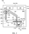
- FIG. 2 is a plan view of a semiconductor package assembly 500 c in accordance with some embodiments of the disclosure. Elements of the embodiments hereinafter, that are the same or similar as those previously described with reference to FIGS. 1, 3 and 4 , are not repeated for brevity.
- the differences between the semiconductor package assembly 500 a / 500 b and the semiconductor package assembly 500 c is that the semiconductor die (logic die) 100 a / 100 b of the semiconductor package assembly 500 c further includes at least a radio frequency (RF) circuit 360 integrated in the semiconductor die (logic die) 100 a / 100 b for RF applications.
- RF radio frequency
- FIG. 5 is a plan view of semiconductor package assemblies 500 d and 500 e in accordance with some embodiments of the disclosure.
- FIGS. 6-7 are cross-sectional views of FIG. 5 , showing the arrangements of the substrate, the logic die, the memory die and the redistribution layer (RDL) ground trace of the memory die of the semiconductor package assembly shown in FIG. 5 .
- RDL redistribution layer
- the differences between the semiconductor package assembly 500 a / 500 b (shown in FIGS. 1-3 ) and the semiconductor package assembly 500 d is that the memory die 200 a is disposed beside the logic die 100 a . Therefore, the memory die 200 a and the logic die 100 a are mounted on the die-attach surface 701 of the substrate 700 by paste 212 and 112 b , respectively.
- the logic die 100 a is coupled to the substrate 700 through the wire bonding technology.
- the semiconductor die 100 a may be mounted on the die-attached surface 701 of the substrate 700 through an adhesive 112 (for example, paste) between the semiconductor die 100 a and the substrate 700 .
- the first terminal 242 of the RDL ground trace 240 , the pad 250 a of the memory die 200 a and the ground pad 102 of the substrate 700 are arranged close to the first side 220 of the memory die 200 a .
- the second terminal 244 of the RDL ground trace 240 , the ground pad 104 and the pad 150 a of the logic die 100 a are both arranged close to the second side 222 of the memory die 200 a .
- the ground pad 104 is disposed between the logic die 100 a and the memory die 200 a as shown in FIG. 6 .
- FIG. 7 is a cross-sectional view of FIG. 5 , showing the arrangements of the substrate, the logic die, the memory die and the redistribution layer (RDL) ground trace of the memory die of a semiconductor package assembly 500 e .
- RDL redistribution layer
- the logic die 100 b may comprise at least a pad 150 b , which is used for input/output (I/O) connections to ground.
- the pad 150 b serves as a ground pad of the logic die 100 b.
- the memory die 200 b may comprise may comprise a memory I/O die pad 202 and a redistribution layer (RDL) structure 270 b on the memory I/O die pad 202 .
- the RDL structure 270 b may comprise at least a redistribution layer (RDL) trace 240 and at least two pads 250 b and 250 c .
- the RDL trace 240 and the pad 250 b and 250 c are used for input/output (I/O) connections to ground.
- the RDL trace 240 serves as a RDL ground trace 240 .
- the RDL trace 240 is designed to be positioned at a single layered-level of the RDL structure 270 b .
- the two terminals 242 and 244 of the RDL trace 240 are respectively coupled to the pads 250 b and 250 c .
- the pads 250 b and 250 c serve as ground pads of the memory die 200 a .
- the pad 250 b is disposed within the input/output (I/O) pad region 210 as shown in FIG. 5 .
- the pad 250 c is disposed outside of the input/output (I/O) pad region 210 .
- the pad 250 c is disposed close to the terminal 244 of the RDL trace 240 .
- the pad 250 b is designed to be free from being in contact with the pad 250 c.
- the memory die 200 b is flipped upside-down and is coupled to the substrate 700 through conductive structures 266 and 268 .
- the conductive structures 266 and 268 are disposed on the pads 250 b and 250 c , respectively.
- the conductive structures 266 and 268 may include conductive bump structures coupled to the corresponding pads 250 b and 250 c .
- the conductive structure 266 is designed to be free from being in contact with the conductive structure 268 .
- the ground pad 250 b of the memory die 200 b is coupled to the ground pad 102 of the substrate 700 through the conductive structure 266 and an interconnect 300 b .
- the pad 250 c of the memory die 200 b is coupled to the to the ground pad 104 of the substrate 700 through the conductive structure 268 and an interconnect 320 b embedded in the substrate 700 .
- the interconnect 300 b and 320 b are disposed embedded in the substrate 700 .
- the interconnect 300 b and 320 b may comprise circuits.
- the logic die 100 b is flipped upside-down and is coupled to the substrate 700 through a conductive structure 160 .
- the conductive structure 160 is disposed on the pad 150 b .
- the conductive structure 160 may include at least a conductive bump structure coupled to the corresponding pad 150 b .
- the pad 150 b of the logic die 100 b is coupled to the to the ground pad 104 of the substrate 700 through the conductive structure 160 and the interconnect 320 b of the substrate 700 . That is to say, the interconnect 320 b electrically connects to the pad 250 c of the memory die 200 b , the pad 150 b of the logic die 100 b and the ground pad 104 of the substrate 700 .
- the interconnect 300 b and the interconnect 320 b are discrete circuits.
- the interconnect 300 b is designed to be free from being in contact with the interconnect 320 b.
- Embodiments provide a semiconductor package assembly.
- the semiconductor package assembly includes a substrate, a memory die and a logic die mounted on the substrate.
- the memory die includes a redistribution layer (RDL) ground trace having a first terminal and a second terminal far away from the first terminal. The first and second terminals are located close to different sides of the memory die.
- the first terminal of the RDL ground trace is coupled to the first ground pad of the substrate through a first conductive path comprising a pad of the memory die, which is positioned within an input/output (I/O) pad region.
- the second terminal of the RDL ground trace is coupled to the second ground pad of the substrate through a second conductive path different from the first conductive path.
- the second conductive path is free from being coupled to the pad of the memory die.
- the logic die includes a pad coupled to the second terminal of the RDL ground trace through the second ground pad of the substrate.
- the semiconductor package assembly is designed to have grounding paths at the two terminals of the redistribution layer (RDL) ground trace of the memory die.
- RDL redistribution layer
- the design of the RDL ground trace can improve signal integrity by reducing the crosstalk problem.
- the semiconductor package assembly includes integrated radio frequency (RF) circuits in the logic die for RF applications, the RDL ground trace of the memory die also can improve the RF desense problem by reducing the coupled noise from the circuit of the memory die to the RF circuit of the logic die.
- RF radio frequency
Landscapes
- Engineering & Computer Science (AREA)
- Microelectronics & Electronic Packaging (AREA)
- Power Engineering (AREA)
- Physics & Mathematics (AREA)
- Computer Hardware Design (AREA)
- General Physics & Mathematics (AREA)
- Condensed Matter Physics & Semiconductors (AREA)
- Geometry (AREA)
- Health & Medical Sciences (AREA)
- Electromagnetism (AREA)
- Toxicology (AREA)
- Semiconductor Memories (AREA)
- Semiconductor Integrated Circuits (AREA)
Priority Applications (4)
| Application Number | Priority Date | Filing Date | Title |
|---|---|---|---|
| US15/411,077 US10679949B2 (en) | 2016-03-11 | 2017-01-20 | Semiconductor package assembly with redistribution layer (RDL) trace |
| EP17154808.4A EP3217429B1 (en) | 2016-03-11 | 2017-02-06 | Semiconductor package assembly |
| CN201710067544.3A CN107180826B (zh) | 2016-03-11 | 2017-02-07 | 半导体封装组件 |
| TW106106100A TWI702703B (zh) | 2016-03-11 | 2017-02-23 | 半導體封裝元件 |
Applications Claiming Priority (2)
| Application Number | Priority Date | Filing Date | Title |
|---|---|---|---|
| US201662306659P | 2016-03-11 | 2016-03-11 | |
| US15/411,077 US10679949B2 (en) | 2016-03-11 | 2017-01-20 | Semiconductor package assembly with redistribution layer (RDL) trace |
Publications (2)
| Publication Number | Publication Date |
|---|---|
| US20170263570A1 US20170263570A1 (en) | 2017-09-14 |
| US10679949B2 true US10679949B2 (en) | 2020-06-09 |
Family
ID=57965834
Family Applications (1)
| Application Number | Title | Priority Date | Filing Date |
|---|---|---|---|
| US15/411,077 Active US10679949B2 (en) | 2016-03-11 | 2017-01-20 | Semiconductor package assembly with redistribution layer (RDL) trace |
Country Status (4)
| Country | Link |
|---|---|
| US (1) | US10679949B2 (zh) |
| EP (1) | EP3217429B1 (zh) |
| CN (1) | CN107180826B (zh) |
| TW (1) | TWI702703B (zh) |
Families Citing this family (9)
| Publication number | Priority date | Publication date | Assignee | Title |
|---|---|---|---|---|
| US9899238B2 (en) * | 2014-12-18 | 2018-02-20 | Intel Corporation | Low cost package warpage solution |
| JP2016192447A (ja) * | 2015-03-30 | 2016-11-10 | 株式会社東芝 | 半導体装置 |
| CN109712943B (zh) * | 2017-10-26 | 2020-11-20 | 联发科技股份有限公司 | 半导体封装组件 |
| CN108962301B (zh) * | 2018-05-24 | 2022-04-12 | 济南德欧雅安全技术有限公司 | 一种存储装置 |
| US10573602B2 (en) * | 2018-06-22 | 2020-02-25 | Nanya Technology Corporation | Semiconductor device and method of forming the same |
| US11404388B2 (en) | 2019-04-29 | 2022-08-02 | Qualcomm Incorporated | Surface mount passive component shorted together and a die |
| US11202375B2 (en) * | 2019-04-29 | 2021-12-14 | Qualcomm Incorporated | Surface mount passive component shorted together |
| JP7279258B2 (ja) * | 2019-10-17 | 2023-05-22 | 長江存儲科技有限責任公司 | 限られた数の試験ピンを使用するメモリデバイスを試験する方法およびその方法を使用するメモリデバイス |
| CN114188312B (zh) * | 2022-02-17 | 2022-07-08 | 甬矽电子(宁波)股份有限公司 | 封装屏蔽结构和屏蔽结构制作方法 |
Citations (11)
| Publication number | Priority date | Publication date | Assignee | Title |
|---|---|---|---|---|
| US5994766A (en) * | 1998-09-21 | 1999-11-30 | Vlsi Technology, Inc. | Flip chip circuit arrangement with redistribution layer that minimizes crosstalk |
| US20050253278A1 (en) | 2004-04-30 | 2005-11-17 | Lam Ken M | Universal interconnect die |
| US20070187814A1 (en) | 2006-02-10 | 2007-08-16 | Cusack Michael D | System and method for routing supply voltages or other signals between side-by-side die and a lead frame for system in a package (SIP) devices |
| US20090004781A1 (en) * | 2007-06-28 | 2009-01-01 | Chien-Ko Liao | Method of fabricating a semiconductor die having a redistribution layer |
| US20110254145A1 (en) * | 2007-11-13 | 2011-10-20 | Hynix Semiconductor Inc. | Stacked semiconductor package |
| CN102484101A (zh) | 2009-08-13 | 2012-05-30 | SKLink株式会社 | 电路基板及其制造方法 |
| US20140185264A1 (en) * | 2012-12-28 | 2014-07-03 | Taiwan Semiconductor Manufacturing Company, Ltd. | Methods and apparatus for forming package-on-packages |
| US20140191376A1 (en) | 2013-01-08 | 2014-07-10 | Siliconware Precision Industries Co., Ltd. | Semiconductor package and fabrication method thereof |
| US20140247634A1 (en) | 2011-10-06 | 2014-09-04 | Fuji Electric Co., Ltd. | Three-level power conversion circuit system |
| US20150206855A1 (en) * | 2014-01-22 | 2015-07-23 | Mediatek Inc. | Semiconductor package |
| US20150318264A1 (en) | 2014-04-30 | 2015-11-05 | Taiwan Semiconductor Manufacturing Company, Ltd. | Stacked Dies With Wire Bonds and Method |
Family Cites Families (1)
| Publication number | Priority date | Publication date | Assignee | Title |
|---|---|---|---|---|
| KR101924388B1 (ko) * | 2011-12-30 | 2018-12-04 | 삼성전자주식회사 | 재배선 구조를 갖는 반도체 패키지 |
-
2017
- 2017-01-20 US US15/411,077 patent/US10679949B2/en active Active
- 2017-02-06 EP EP17154808.4A patent/EP3217429B1/en active Active
- 2017-02-07 CN CN201710067544.3A patent/CN107180826B/zh active Active
- 2017-02-23 TW TW106106100A patent/TWI702703B/zh active
Patent Citations (13)
| Publication number | Priority date | Publication date | Assignee | Title |
|---|---|---|---|---|
| US5994766A (en) * | 1998-09-21 | 1999-11-30 | Vlsi Technology, Inc. | Flip chip circuit arrangement with redistribution layer that minimizes crosstalk |
| US20050253278A1 (en) | 2004-04-30 | 2005-11-17 | Lam Ken M | Universal interconnect die |
| US20070187814A1 (en) | 2006-02-10 | 2007-08-16 | Cusack Michael D | System and method for routing supply voltages or other signals between side-by-side die and a lead frame for system in a package (SIP) devices |
| US20090004781A1 (en) * | 2007-06-28 | 2009-01-01 | Chien-Ko Liao | Method of fabricating a semiconductor die having a redistribution layer |
| US20110254145A1 (en) * | 2007-11-13 | 2011-10-20 | Hynix Semiconductor Inc. | Stacked semiconductor package |
| US20120193799A1 (en) * | 2009-08-13 | 2012-08-02 | SKLink Co., Ltd. | Circuit substrate and method of manufacturing same |
| CN102484101A (zh) | 2009-08-13 | 2012-05-30 | SKLink株式会社 | 电路基板及其制造方法 |
| US8508046B2 (en) | 2009-08-13 | 2013-08-13 | Disco Corporation | Circuit substrate and method of manufacturing same |
| US20140247634A1 (en) | 2011-10-06 | 2014-09-04 | Fuji Electric Co., Ltd. | Three-level power conversion circuit system |
| US20140185264A1 (en) * | 2012-12-28 | 2014-07-03 | Taiwan Semiconductor Manufacturing Company, Ltd. | Methods and apparatus for forming package-on-packages |
| US20140191376A1 (en) | 2013-01-08 | 2014-07-10 | Siliconware Precision Industries Co., Ltd. | Semiconductor package and fabrication method thereof |
| US20150206855A1 (en) * | 2014-01-22 | 2015-07-23 | Mediatek Inc. | Semiconductor package |
| US20150318264A1 (en) | 2014-04-30 | 2015-11-05 | Taiwan Semiconductor Manufacturing Company, Ltd. | Stacked Dies With Wire Bonds and Method |
Also Published As
| Publication number | Publication date |
|---|---|
| TWI702703B (zh) | 2020-08-21 |
| EP3217429A1 (en) | 2017-09-13 |
| US20170263570A1 (en) | 2017-09-14 |
| CN107180826A (zh) | 2017-09-19 |
| TW201806111A (zh) | 2018-02-16 |
| CN107180826B (zh) | 2020-06-19 |
| EP3217429B1 (en) | 2021-11-17 |
Similar Documents
| Publication | Publication Date | Title |
|---|---|---|
| US10679949B2 (en) | Semiconductor package assembly with redistribution layer (RDL) trace | |
| US9978729B2 (en) | Semiconductor package assembly | |
| US10361173B2 (en) | Semiconductor package assemblies with system-on-chip (SOC) packages | |
| US10332830B2 (en) | Semiconductor package assembly | |
| US10177125B2 (en) | Semiconductor package assembly | |
| US10217724B2 (en) | Semiconductor package assembly with embedded IPD | |
| US20150206855A1 (en) | Semiconductor package | |
| US11837552B2 (en) | Semiconductor package with layer structures, antenna layer and electronic component | |
| US9997498B2 (en) | Semiconductor package assembly | |
| US9331054B2 (en) | Semiconductor package assembly with decoupling capacitor | |
| US10074621B2 (en) | Electronic package with antenna structure | |
| US10147674B2 (en) | Semiconductor package assembly | |
| US10497678B2 (en) | Semiconductor package assembly with passive device | |
| US20170294407A1 (en) | Passive element package and semiconductor module comprising the same | |
| CN112447690B (zh) | 天线置顶的半导体封装结构 | |
| US20220319970A1 (en) | Semiconductor package |
Legal Events
| Date | Code | Title | Description |
|---|---|---|---|
| AS | Assignment |
Owner name: MEDIATEK INC., TAIWAN Free format text: ASSIGNMENT OF ASSIGNORS INTEREST;ASSIGNORS:LIN, SHENG-MOU;HO, DUEN-YI;REEL/FRAME:041025/0473 Effective date: 20170118 |
|
| STPP | Information on status: patent application and granting procedure in general |
Free format text: RESPONSE TO NON-FINAL OFFICE ACTION ENTERED AND FORWARDED TO EXAMINER |
|
| STPP | Information on status: patent application and granting procedure in general |
Free format text: FINAL REJECTION MAILED |
|
| STPP | Information on status: patent application and granting procedure in general |
Free format text: DOCKETED NEW CASE - READY FOR EXAMINATION |
|
| STPP | Information on status: patent application and granting procedure in general |
Free format text: NOTICE OF ALLOWANCE MAILED -- APPLICATION RECEIVED IN OFFICE OF PUBLICATIONS |
|
| STPP | Information on status: patent application and granting procedure in general |
Free format text: AWAITING TC RESP, ISSUE FEE PAYMENT VERIFIED |
|
| STPP | Information on status: patent application and granting procedure in general |
Free format text: PUBLICATIONS -- ISSUE FEE PAYMENT VERIFIED |
|
| STCF | Information on status: patent grant |
Free format text: PATENTED CASE |
|
| CC | Certificate of correction | ||
| MAFP | Maintenance fee payment |
Free format text: PAYMENT OF MAINTENANCE FEE, 4TH YEAR, LARGE ENTITY (ORIGINAL EVENT CODE: M1551); ENTITY STATUS OF PATENT OWNER: LARGE ENTITY Year of fee payment: 4 |