US10657886B2 - Pixel compensation circuit, driving method thereof and display device - Google Patents
Pixel compensation circuit, driving method thereof and display device Download PDFInfo
- Publication number
- US10657886B2 US10657886B2 US15/278,864 US201615278864A US10657886B2 US 10657886 B2 US10657886 B2 US 10657886B2 US 201615278864 A US201615278864 A US 201615278864A US 10657886 B2 US10657886 B2 US 10657886B2
- Authority
- US
- United States
- Prior art keywords
- switching transistor
- output
- circuit
- driving
- light
- Prior art date
- Legal status (The legal status is an assumption and is not a legal conclusion. Google has not performed a legal analysis and makes no representation as to the accuracy of the status listed.)
- Active, expires
Links
- 238000000034 method Methods 0.000 title claims abstract description 14
- 239000003990 capacitor Substances 0.000 claims abstract description 120
- 230000003071 parasitic effect Effects 0.000 claims description 14
- 239000010409 thin film Substances 0.000 claims description 2
- 238000004088 simulation Methods 0.000 description 6
- 238000010586 diagram Methods 0.000 description 5
- 238000011017 operating method Methods 0.000 description 3
- 238000012986 modification Methods 0.000 description 2
- 230000004048 modification Effects 0.000 description 2
- 241001673391 Entandrophragma candollei Species 0.000 description 1
- 230000002159 abnormal effect Effects 0.000 description 1
- 238000005516 engineering process Methods 0.000 description 1
- 239000000463 material Substances 0.000 description 1
- 230000000750 progressive effect Effects 0.000 description 1
Images


Classifications
-
- G—PHYSICS
- G09—EDUCATION; CRYPTOGRAPHY; DISPLAY; ADVERTISING; SEALS
- G09G—ARRANGEMENTS OR CIRCUITS FOR CONTROL OF INDICATING DEVICES USING STATIC MEANS TO PRESENT VARIABLE INFORMATION
- G09G3/00—Control arrangements or circuits, of interest only in connection with visual indicators other than cathode-ray tubes
- G09G3/20—Control arrangements or circuits, of interest only in connection with visual indicators other than cathode-ray tubes for presentation of an assembly of a number of characters, e.g. a page, by composing the assembly by combination of individual elements arranged in a matrix no fixed position being assigned to or needed to be assigned to the individual characters or partial characters
- G09G3/22—Control arrangements or circuits, of interest only in connection with visual indicators other than cathode-ray tubes for presentation of an assembly of a number of characters, e.g. a page, by composing the assembly by combination of individual elements arranged in a matrix no fixed position being assigned to or needed to be assigned to the individual characters or partial characters using controlled light sources
- G09G3/30—Control arrangements or circuits, of interest only in connection with visual indicators other than cathode-ray tubes for presentation of an assembly of a number of characters, e.g. a page, by composing the assembly by combination of individual elements arranged in a matrix no fixed position being assigned to or needed to be assigned to the individual characters or partial characters using controlled light sources using electroluminescent panels
- G09G3/32—Control arrangements or circuits, of interest only in connection with visual indicators other than cathode-ray tubes for presentation of an assembly of a number of characters, e.g. a page, by composing the assembly by combination of individual elements arranged in a matrix no fixed position being assigned to or needed to be assigned to the individual characters or partial characters using controlled light sources using electroluminescent panels semiconductive, e.g. using light-emitting diodes [LED]
- G09G3/3208—Control arrangements or circuits, of interest only in connection with visual indicators other than cathode-ray tubes for presentation of an assembly of a number of characters, e.g. a page, by composing the assembly by combination of individual elements arranged in a matrix no fixed position being assigned to or needed to be assigned to the individual characters or partial characters using controlled light sources using electroluminescent panels semiconductive, e.g. using light-emitting diodes [LED] organic, e.g. using organic light-emitting diodes [OLED]
- G09G3/3225—Control arrangements or circuits, of interest only in connection with visual indicators other than cathode-ray tubes for presentation of an assembly of a number of characters, e.g. a page, by composing the assembly by combination of individual elements arranged in a matrix no fixed position being assigned to or needed to be assigned to the individual characters or partial characters using controlled light sources using electroluminescent panels semiconductive, e.g. using light-emitting diodes [LED] organic, e.g. using organic light-emitting diodes [OLED] using an active matrix
- G09G3/3233—Control arrangements or circuits, of interest only in connection with visual indicators other than cathode-ray tubes for presentation of an assembly of a number of characters, e.g. a page, by composing the assembly by combination of individual elements arranged in a matrix no fixed position being assigned to or needed to be assigned to the individual characters or partial characters using controlled light sources using electroluminescent panels semiconductive, e.g. using light-emitting diodes [LED] organic, e.g. using organic light-emitting diodes [OLED] using an active matrix with pixel circuitry controlling the current through the light-emitting element
-
- G—PHYSICS
- G09—EDUCATION; CRYPTOGRAPHY; DISPLAY; ADVERTISING; SEALS
- G09G—ARRANGEMENTS OR CIRCUITS FOR CONTROL OF INDICATING DEVICES USING STATIC MEANS TO PRESENT VARIABLE INFORMATION
- G09G2300/00—Aspects of the constitution of display devices
- G09G2300/08—Active matrix structure, i.e. with use of active elements, inclusive of non-linear two terminal elements, in the pixels together with light emitting or modulating elements
- G09G2300/0809—Several active elements per pixel in active matrix panels
- G09G2300/0819—Several active elements per pixel in active matrix panels used for counteracting undesired variations, e.g. feedback or autozeroing
-
- G—PHYSICS
- G09—EDUCATION; CRYPTOGRAPHY; DISPLAY; ADVERTISING; SEALS
- G09G—ARRANGEMENTS OR CIRCUITS FOR CONTROL OF INDICATING DEVICES USING STATIC MEANS TO PRESENT VARIABLE INFORMATION
- G09G2300/00—Aspects of the constitution of display devices
- G09G2300/08—Active matrix structure, i.e. with use of active elements, inclusive of non-linear two terminal elements, in the pixels together with light emitting or modulating elements
- G09G2300/0809—Several active elements per pixel in active matrix panels
- G09G2300/0842—Several active elements per pixel in active matrix panels forming a memory circuit, e.g. a dynamic memory with one capacitor
- G09G2300/0861—Several active elements per pixel in active matrix panels forming a memory circuit, e.g. a dynamic memory with one capacitor with additional control of the display period without amending the charge stored in a pixel memory, e.g. by means of additional select electrodes
-
- G—PHYSICS
- G09—EDUCATION; CRYPTOGRAPHY; DISPLAY; ADVERTISING; SEALS
- G09G—ARRANGEMENTS OR CIRCUITS FOR CONTROL OF INDICATING DEVICES USING STATIC MEANS TO PRESENT VARIABLE INFORMATION
- G09G2310/00—Command of the display device
- G09G2310/02—Addressing, scanning or driving the display screen or processing steps related thereto
- G09G2310/0264—Details of driving circuits
- G09G2310/0297—Special arrangements with multiplexing or demultiplexing of display data in the drivers for data electrodes, in a pre-processing circuitry delivering display data to said drivers or in the matrix panel, e.g. multiplexing plural data signals to one D/A converter or demultiplexing the D/A converter output to multiple columns
-
- G—PHYSICS
- G09—EDUCATION; CRYPTOGRAPHY; DISPLAY; ADVERTISING; SEALS
- G09G—ARRANGEMENTS OR CIRCUITS FOR CONTROL OF INDICATING DEVICES USING STATIC MEANS TO PRESENT VARIABLE INFORMATION
- G09G2310/00—Command of the display device
- G09G2310/08—Details of timing specific for flat panels, other than clock recovery
-
- G—PHYSICS
- G09—EDUCATION; CRYPTOGRAPHY; DISPLAY; ADVERTISING; SEALS
- G09G—ARRANGEMENTS OR CIRCUITS FOR CONTROL OF INDICATING DEVICES USING STATIC MEANS TO PRESENT VARIABLE INFORMATION
- G09G2320/00—Control of display operating conditions
- G09G2320/02—Improving the quality of display appearance
- G09G2320/0219—Reducing feedthrough effects in active matrix panels, i.e. voltage changes on the scan electrode influencing the pixel voltage due to capacitive coupling
-
- G—PHYSICS
- G09—EDUCATION; CRYPTOGRAPHY; DISPLAY; ADVERTISING; SEALS
- G09G—ARRANGEMENTS OR CIRCUITS FOR CONTROL OF INDICATING DEVICES USING STATIC MEANS TO PRESENT VARIABLE INFORMATION
- G09G2320/00—Control of display operating conditions
- G09G2320/02—Improving the quality of display appearance
- G09G2320/0223—Compensation for problems related to R-C delay and attenuation in electrodes of matrix panels, e.g. in gate electrodes or on-substrate video signal electrodes
-
- G—PHYSICS
- G09—EDUCATION; CRYPTOGRAPHY; DISPLAY; ADVERTISING; SEALS
- G09G—ARRANGEMENTS OR CIRCUITS FOR CONTROL OF INDICATING DEVICES USING STATIC MEANS TO PRESENT VARIABLE INFORMATION
- G09G2320/00—Control of display operating conditions
- G09G2320/02—Improving the quality of display appearance
- G09G2320/0233—Improving the luminance or brightness uniformity across the screen
Definitions
- Embodiments of the present disclosure relate to a pixel compensation circuit, a driving method thereof and a display device.
- OLED organic light-emitting diode
- a pixel compensation circuit including: a signal input unit, a driving unit, a light-emitting control unit, a first reset unit, a second reset unit, a first storage capacitor, a first switching transistor and a second switching transistor, wherein the signal input unit is connected with an input of the first switching transistor; a signal write control line is connected with a control end of the first switching transistor; an output of the second switching transistor, the second reset unit and one end of the first storage capacitor are respectively connected with an output of the first switching transistor; the first reset unit and the driving unit are respectively connected with the other end of the first storage capacitor; an output of first reference voltage is connected with an input of the second switching transistor; a first scanning signal line is connected with a control end of the second switching transistor; a high-level output of a power supply, the driving unit and the light-emitting control unit are sequentially connected with one to another; a light-emitting control signal line is connected with the light-emitting control unit; and when
- Embodiments of the present disclosure also provide a display device, including the pixel compensation circuit.
- Embodiments of the present disclosure also provide a driving method of the pixel compensation circuit, including: in a reset period, a signal input unit does not operate; a driving unit does not operate; a light-emitting control unit does not operate; a signal write control line controls a first switching transistor to be switched off; a first scanning signal line controls a second switching transistor to be switched off; a first reset unit resets one end of a first storage capacitor connected with an end of the driving unit; a second reset unit resets one end of the first storage capacitor connected with the output of the first switching transistor; in a compensating period, the signal input unit does not operate; the driving unit begins to operate; the light-emitting control unit does not operate; the signal write control line controls the first switching transistor to be switched off; the first scanning signal line controls the second switching transistor to be switched on; both the first reset unit and the second reset unit stop resetting; the driving unit begins to operate, so that a high-level output of a power supply can charge the first storage capacitor; after the second switching transistor is switched
- FIG. 1 is a schematic diagram of a pixel compensation circuit provided by an embodiment of the present disclosure
- FIG. 2 is a signal timing sequence chart of a driving method of a pixel compensation circuit, provided by an embodiment of the present disclosure
- FIG. 3 is a schematic structural view of a multiplexer in an embodiment of the present disclosure
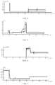
- FIG. 4 is a simulating result diagram of drive current corresponding to different data line capacitors
- FIG. 5 is a simulating result diagram of electric potential of N 2 nodes corresponding to different data line capacitors
- FIG. 6 is a simulating result diagram of drive current corresponding to different data line capacitors in an embodiment of the present disclosure.
- shape of the display of the OLED display device is more and more diversified; as for some displays with special shapes (e.g., circular, oval and polygonal), the number of pixel units corresponding to each column on the display is different; as the number and the capacitance of parasitic capacitors corresponding to each pixel unit is same and the data line capacitor corresponding to each column of pixel units is created by the parallel connection of the parasitic capacitors corresponding to this column of pixel units, the capacitance of the data line capacitor corresponding to each column of pixel units on the display with special shape is different; in this case, when display data voltage is written into corresponding sub-pixel units through the data line capacitor, display data voltage which is actually written into the sub-pixel units is the result of the voltage dividing of the data line capacitor and the storage capacitor corresponding to the pixel unit; and when same display data are inputted into the display with special shape, thus the brightness of light emitted by different columns of pixel units is different.
- special shapes e.g., circular, oval and polygonal
- the pixel compensation circuit includes: a signal input unit 1 , a driving unit 2 , a light-emitting control unit 3 , a first reset unit 4 , a second reset unit 5 , a first storage capacitor C 1 , a first switching transistor T 1 and a second switching transistor T 2 .
- the signal input unit 1 is connected with an input of the first switching transistor T 1 ; a signal write control line T n is connected with a control end of the first switching transistor T 1 ; an output of the second switching transistor T 2 , the second reset unit 5 and one end of the first storage capacitor C 1 are respectively connected with an output of the first switching transistor T 1 ; the first reset unit 4 and the driving unit 2 are respectively connected with the other end of the first storage capacitor C 1 ; an output of first reference voltage Vref is connected with an input of the second switching transistor T 2 ; a first scanning signal line G (n) is connected with a control end of the second switching transistor T 2 ; a high-level output of a power supply, the driving unit 2 and the light-emitting control unit 3 are sequentially connected with one to another; a light-emitting control signal line EM (n) is connected with the light-emitting control unit 3 ; and when display data are written into the signal input unit 1 , the signal write control line T n controls the first switching transistor T 1 to
- junctions of the output of the first switching transistor T 1 , the output of the second switching transistor T 2 , the second reset unit 5 and one end of the first storage capacitor C 1 are defined to be N 2 nodes, and junctions of the other end of the first storage capacitor C 1 , the first reset unit 4 and the driving unit 2 are defined to be N 1 nodes.
- the signal input unit 1 does not operate; the driving unit 2 does not operate; the light-emitting control signal line EM (n) controls the light-emitting control unit 3 to not operate; the signal write control line T n controls the first switching transistor T 1 to be switched off; the first scanning signal line G (n) controls the second switching transistor T 2 to be switched off; the first reset unit 4 is configured to reset the N 1 nodes; and the second reset unit 5 resets the N 2 nodes.
- the signal input unit 1 does not operate; the driving unit 2 begins to operate; the light-emitting control signal line EM (n) controls the light-emitting control unit 3 to not operate; the signal write control line T n controls the first switching transistor T 1 to be switched off; the first scanning signal line G (n) controls the second switching transistor T 2 to be switched on; both the first reset unit 4 and the second reset unit 5 stop resetting; the driving unit 2 begins to operate, so that the high-level output of the power supply can charge the first storage capacitor T 1 ; after the second switching transistor T 2 is switched on, the output of the first reference voltage Vref charges the first storage capacitor C 1 , and the electric potential of the N 2 nodes is converted into the first reference voltage Vref.
- the signal input unit 1 begins to operate; the driving unit 2 does not operate; the light-emitting control signal line EM (n) controls the light-emitting control unit 3 to not operate; the signal write control line T n controls the first switching transistor T 1 to be switched on; the first scanning signal line G (n) controls the second switching transistor T 2 to be switched off; both the first reset unit 4 and the second reset unit 5 stop resetting; when the first switching transistor T 1 is switched on, the signal input unit 1 begins to operate and charges the first storage capacitor C 1 , so that the electric potential of the N 2 nodes is converted into display data voltage V data written into the signal input unit 1 ; and both the driving unit 2 and the first reset unit 4 do not operate, so that one end of the first storage capacitor C 1 connected with the N 1 node is in the floating state, and the electric potential of the N 1 node responds to the jump in potential of the N 2 node.
- the signal input unit 1 does not operate; the driving unit 2 begins to operate; the light-emitting control signal line EM (n) controls the light-emitting control unit 3 to begin to operate; the signal write control line T n controls the first switching transistor T 1 to be switched off; the first scanning signal line G (n) controls the second switching transistor T 2 to be switched off; both the first reset unit 4 and the second reset unit 5 stop resetting; and as the light-emitting control signal line EM (n) controls the light-emitting control unit 3 to begin to operate, in this case, the driving unit 2 operates in a saturation region and generates drive current I oled , and the generated drive current I oled can drive the light-emitting control unit 3 to emit light.
- the driving unit 2 operates in a saturation region and generates drive current I oled , and the generated drive current I oled can drive the light-emitting control unit 3 to emit light.
- the signal write control line T n can control the first switching transistor T 1 to be switched on. In this way, after written into the signal input unit 1 , the display data voltage V data can be directly output to the N 2 node through the first switching transistor T 1 by the signal input unit 1 , and it is not required that the display data voltage V data is stored in the data line capacitor at first by the signal input unit 1 and then output to the N 2 node by the data line capacitor.
- the display data voltage V data written into the signal input unit 1 can be completely output to the N 2 node, which is not the result of voltage dividing of the data line capacitor corresponding to this column of pixel units and the storage capacitor corresponding to the pixel unit. That is to say, when a same display data voltage V data is inputted into a display with special shape, the brightness of light emitted by different columns of pixel units is same.
- the pixel compensation circuit provided by the embodiment of the present disclosure, other devices are not required to be arranged on the periphery of the pixel compensation circuit to completely and consistently compensate the capacitance of the data line capacitors corresponding to different columns of pixel units, so that the problem of non-uniform light emitted by the pixel units caused by different capacitance of the data line capacitors can be avoided, which can well satisfy the narrow-bezel development requirement of the OLED display device.
- the signal write control line T n controls the first switching transistor T 1 to be switched off; the first scanning signal line G (n) controls the second switching transistor T 2 to be switched off; and the second reset unit 5 stops resetting.
- one end of the first storage capacitor C 1 connected with the N 2 node is in the floating state.
- the floating state likely leads to a phenomenon of signal crosstalk in the pixel compensation circuit, and the display of the OLED display device can be abnormal.
- a second storage capacitor C 2 is introduced into the pixel compensation circuit provided by the present embodiment; one end of the second storage capacitor C 2 is connected with the high-level output of the power supply; the other end of the second storage capacitor C 2 is connected with the output of the first switching transistor T 1 ; the other end of the second storage capacitor C 2 is connected with the output of the second switching transistor T 2 ; and the other end of the second storage capacitor C 2 is connected with one end of the first storage capacitor C 1 .
- the second storage capacitor C 2 is introduced in, one end of the first storage capacitor C 1 connected with the N 2 node is connected with the high-level output of the power supply through the second storage capacitor C 2 .
- the driving unit 2 provided by the embodiment includes a driving switching transistor DTFT and a third switching transistor T 3 .
- a control end of the driving switching transistor DTFT is connected with an output of the third switching transistor T 3 ;
- the control end of the driving switching transistor DTFT is connected with the first reset unit 4 ;
- the control end of the driving switching transistor DTFT is connected with the other end of the first storage capacitor C 1 ;
- an input of the driving switching transistor DTFT is connected with the high-level output of the power supply;
- an output of the driving switching transistor DTFT is connected with an input of the third switching transistor T 3 ;
- the output of the driving switching transistor DTFT is connected with the light-emitting control unit 3 ;
- the first scanning signal line G (n) is connected with a control end of the third switching transistor T 3 .
- the driving switching transistor DTFT has many types and may select P-channel thin film transistor (TFT) or N-channel TFT.
- TFT thin film transistor
- the input of the driving switching transistor DTFT is a source electrode and the output of the driving switching transistor DTFT is a drain electrode.
- the first scanning signal line G (n) controls the third switching transistor T 3 to be switched on, and the control end of the driving switching transistor DTFT is shorted with the output of the driving switching transistor DTFT, so that the driving switching transistor DTFT can have the characteristic of forward conduction of a common diode.
- V th is a positive value; and when the driving switching transistor DTFT is a P-channel TFT, V th is a negative value.
- the signal input unit 1 operates; the first switching transistor T 1 is switched on; and the display data voltage V data is written into corresponding pixel unit.
- the electric potential of the N 2 node jumps from the first reference voltage Vref to the display data voltage V data .
- the first scanning signal line G (n) controls the third switching transistor T 3 to be switched off and the light-emitting control signal line EM (n) controls the light-emitting control unit 3 to begins to operate.
- the driving unit 2 operates in the saturation region and generates the drive current I oled .
- I oled 1 ⁇ 2 k ( V gs ⁇ V th ) Equation 4
- k in the equation 4 and the equation 5 is a constant.
- the drive current I oled is only related to the display data voltage V data and the first reference voltage Vref and is not related to the supply voltage VDD and the threshold voltage V th . In this way, the influence of the attenuation of the supply voltage VDD on the drive current I oled and the influence of the threshold voltage V th on the drive current I oled can be avoided.
- the light-emitting control unit 3 provided by the embodiment includes a fourth switching transistor T 4 and a light-emitting component.
- a control end of the fourth switching transistor T 4 is connected with the light-emitting control signal line EM (n) ; an input of the fourth switching transistor T 4 is connected with the output of the driving switching transistor DTFT; the input of the fourth switching transistor T 4 is connected with the input of the third switching transistor T 3 ; an output of the fourth switching transistor T 4 is connected with an positive pole of the light-emitting component; and a negative pole of the light-emitting component is connected with a common ground VSS.
- the driving unit 2 may generate the drive current I oled , but the generated drive current I oled is not the drive current required by the light-emitting component.
- the light-emitting control signal line EM (n) controls the fourth switching transistor T 4 to be switched off, so that the light-emitting component and the driving unit 2 can be in the isolated state, and the problem of flicker due to error driving of the light-emitting component can be avoided, or the problem that the service life of the light-emitting component is affected by high driving frequency can be avoided.
- the t 4 period as shown in FIG.
- the light-emitting control signal line EM (n) controls the fourth switching transistor T 4 to be switched on, so that the drive current I oled can directly drive the light-emitting component to emit light, and the OLED display device can display an image.
- the light-emitting component has many types, and mostly used light-emitting component is an OLED, but the embodiments of the present disclosure are not limited thereto.
- the structures of the first reset unit 4 and the second reset unit 5 can be many types, so that the reset function of the first reset unit 4 and the second reset unit 5 can be achieved.
- the structures of the first reset unit 4 and the second reset unit 5 will be given below for describing the operating procedure of the first reset unit 4 and the second reset unit 5 .
- the first reset unit 4 includes a fifth switching transistor T 5 ; the second reset unit 5 includes a sixth switching transistor T 6 ; a control end of the fifth switching transistor T 5 and a control end of the sixth switching transistor T 6 are respectively connected with a second scanning signal line; an output of second reference voltage Vinit is connected with an input of the fifth switching transistor T 5 ; an output of the fifth switching transistor T 5 is connected with the control end of the driving switching transistor DTFT; the output of the fifth switching transistor T 5 is connected with the output of the third switching transistor T 3 ; the output of the fifth switching transistor T 5 is connected with the other end of the first storage capacitor C 1 ; the output of the first reference voltage Vref is connected with an input of the sixth switching transistor T 6 ; an output of the sixth switching transistor T 6 is connected with the output of the second switching transistor T 2 ; the output of the sixth switching transistor T 6 is connected with the output of the first switching transistor T 1 ; and the output of the sixth switching transistor T 6 is connected with one end of the first storage capacitor C 1 .
- the second scanning signal line G (n-1) controls the fifth switching transistor T 5 and the sixth switching transistor T 6 to be switched on, so that the electric potential of the N 1 node can be reset to be the second reference voltage Vinit by the output of the second reference voltage Vinit through the fifth switching transistor T 5 , and the electric potential of the N 2 node can be reset to be the first reference voltage Vref by the output of the first reference voltage Vref through the sixth switching transistor T 6 .
- both the first reference voltage Vref and the second reference voltage Vinit are stable DC voltage, namely they will not have phenomenon, such as attenuation, or instability.
- the signal input unit 1 may have many structures. For example, it may be formed by an independent switching transistor and a parasitic capacitor C 3 , and may also be formed by partial switching transistors in a multiplexor (MUX) and the parasitic capacitor C 3 . As shown in FIG. 3 , when the MUX is selected to provide data signal voltage for the pixel compensation circuit, one switching transistor in the MUX is selected to form a signal input unit with the parasitic capacitor C 3 .
- MUX multiplexor
- the signal input unit includes a seventh switching transistor T 7 and the parasitic capacitor C 3 ; a display data line is connected with an input of the seventh switching transistor T 7 ; an output of the seventh switching transistor T 7 is connected with one end of the parasitic capacitor C 3 ; the output of the seventh switching transistor T 7 is connected with the input of the first switching transistor T 1 ; the other end of the parasitic capacitor C 3 is connected with the common ground VSS; and the seventh switching transistor T 7 is controlled to be switched on by a control signal connected with the control end of the seventh switching transistor T 7 in the MUX, so that the display data voltage V data can be written into the pixel compensation circuit.
- the signal write control line T n controls the first switching transistor T 1 to be switched on.
- the multiplexor controls the seventh switching transistor T 7 , an eighth switching transistor MUX 2 and a ninth switching transistor MUX 3 therein to be switched on sequentially, so that corresponding first display data voltage V data1 , second display data voltage V data2 and third display data voltage V data3 can be sequentially output to the N 2 nodes of corresponding pixel units through the first switching transistor T 1 .
- the first switching transistor T 1 , the second switching transistor T 2 , the third switching transistor T 3 , the fourth switching transistor T 4 , the fifth switching transistor T 5 , the sixth switching transistor T 6 , the seventh switching transistor T 7 , the eighth switching transistor MUX 2 , the ninth switching transistor MUX 3 and the driving switching transistor DTFT in the embodiment may be P-channel TFTs or other elements capable of achieving the function of a controllable switch, e.g., N-channel TFTs.
- the type of the switching transistors in the same pixel compensation circuit may be same or different, and corresponding timing sequence high and low level can be adjusted according to the characteristics of the threshold voltage V th .
- the pixel compensation circuit provided by the embodiments of the present disclosure can be easily modified into a circuit formed by other elements having the function of controllable switches based on the basic principle of the present pixel compensation circuit.
- the embodiments use such elements shall fall within the scope of the present disclosure.
- the first switching transistor T 1 , the second switching transistor T 2 , the third switching transistor T 3 , the fourth switching transistor T 4 , the fifth switching transistor T 5 , the sixth switching transistor T 6 and the seventh switching transistor T 7 are all P-channel TFTs, corresponding voltage (control end voltage) for driving the first switching transistor T 1 , the second switching transistor T 2 , the third switching transistor T 3 , the fourth switching transistor T 4 , the fifth switching transistor T 5 , the sixth switching transistor T 6 and the seventh switching transistor T 7 to be switched on is all in a low level; the inputs of the switching transistor T 1 , the second switching transistor T 2 , the third switching transistor T 3 , the fourth switching transistor T 4 , the fifth switching transistor T 5 , the sixth switching transistor T 6 and the seventh switching transistor T 7 are all source electrodes; the outputs are all drain electrodes; and the control ends are all gate electrodes.
- data line capacitors with the two capacitances 0.5 pF and 8 pF are selected; the drive current I oled and the electric potential of the N 2 node are respectively subjected to simulation according to the difference between the pixel compensation circuit in the prior art and the pixel compensation circuit provided by an embodiment of the present disclosure.
- the dotted line in each figure represents the case that the capacitance of the data line capacitor is 0.5 pF and the solid line in each figure represents the case that the capacitance of the data line capacitor is 8 pF.
- the x-coordinate in FIGS. 4 to 7 represents time and the unit is ⁇ S, respectively; the y-coordinate in FIGS. 4 and 6 represents drive current I oled and the unit is nA, respectively; and the y-coordinate in FIGS. 5 and 7 represents electric potential of the N 2 node and the unit is V, respectively.
- the difference of the drive current I oled corresponding to the pixel compensation circuit provided by the embodiment of the present disclosure is significantly less than the difference of the drive current I oled corresponding to the pixel compensation circuit in the prior art. It is noted that the period corresponding to the simulation results of FIGS. 4 and 6 is the same working period of the two pixel compensation circuits.
- the display data voltage V data of the pixel compensation circuit provided by the present disclosure can be completely written into corresponding pixel unit, namely the electric potential of the N 2 node corresponding to the pixel compensation circuit is equal to the display data voltage V data .
- the difference is significantly less than the difference of the electric potential of the N 2 node of the pixel compensation circuit in the prior art.
- the timing period corresponding to the simulation results of FIGS. 5 and 7 is the same working period of the two pixel compensation circuits.
- the pixel compensation circuit provided by the embodiments of the present disclosure can well avoid the problem of different brightness of light emitted by the pixel units due to different capacitance of the data line capacitor corresponding to each column of pixel units in the display panel.
- the embodiments of the present disclosure also provide a display device, which includes the pixel compensation circuit.
- the pixel compensation circuit can well avoid the problem of different brightness of light emitted by the pixel units due to different capacitance of the data line capacitor corresponding to each column of pixel units in the display panel, during an images are displayed, the display device provided by the embodiments of the present disclosure can avoid the problem of different brightness of displayed images due to different capacitance of the data line capacitor corresponding to each column of pixel units in the display panel.
- the embodiments of the present disclosure also provide a driving method of a pixel compensation circuit, which is used for driving the pixel compensation circuit and includes:
- the signal input unit 1 does not operate; the driving unit 2 does not operate; the light-emitting control signal line EM (n) controls the light-emitting control unit 3 to not operate; the signal write control line T n controls the first switching transistor T 1 to be switched off; the first scanning signal line G (n) controls the second switching transistor T 2 to be switched off; the first reset unit 4 resets the N 1 nodes; and the second reset unit 5 resets the N 2 node.
- the signal input unit 1 does not operate; the driving unit 2 begins to operate; the light-emitting control signal line EM (n) controls the light-emitting control unit 3 to not operate; the signal write control line T n controls the first switching transistor T 1 to be switched off; the first scanning signal line G (n) controls the second switching transistor T 2 to be switched on; both the first reset unit 4 and the second reset unit 5 stop resetting; the driving unit 2 begins to operate, so that the high-level output of the power supply can charge the first storage capacitor T 1 ; after the second switching transistor T 2 is switched on, the output of the first reference voltage Vref charges the first storage capacitor C 1 , and the electric potential of the N 2 nodes is converted into the first reference voltage Vref.
- the signal input unit 1 begins to operate; the driving unit 2 does not operate; the light-emitting control signal line EM (n) controls the light-emitting control unit 3 to not operate; the signal write control line T n controls the first switching transistor T 1 to be switched on; the first scanning signal line G (n) controls the second switching transistor T 2 to be switched off; both the first reset unit 4 and the second reset unit 5 stop resetting; when the first switching transistor T 1 is switched on, the signal input unit 1 begins to operate and charges the first storage capacitor C 1 , so that the electric potential of the N 2 nodes is converted into a display data voltage V data written into the signal input unit 1 ; and both the driving unit 2 and the first reset unit 4 do not operate, so that one end of the first storage capacitor C 1 connected with the N 1 node is in the floating state, and the electric potential of the N 1 node responds to the jump in potential of the N 2 node.
- the signal input unit 1 does not operate; the driving unit 2 begins to operate; the light-emitting control signal line EM (n) controls the light-emitting control unit 3 to begin to operate; the signal write control line T n controls the first switching transistor T 1 to be switched off; the first scanning signal line G (n) controls the second switching transistor T 2 to be switched off; both the first reset unit 4 and the second reset unit 5 stop resetting; and as the light-emitting control signal line EM(n) controls the light-emitting control unit 3 to begin to operate, in this case, the driving unit 2 operates in a saturation region and generates drive current I oled , and the generated drive current I oled can drive the light-emitting control unit 3 to emit light.
- the driving unit 2 operates in a saturation region and generates drive current I oled , and the generated drive current I oled can drive the light-emitting control unit 3 to emit light.
- the driving unit 2 includes a driving switching transistor DTFT and a third switching transistor T 3 .
- a control end of the driving switching transistor DTFT is connected with an output of the third switching transistor T 3 ;
- the control end of the driving switching transistor DTFT is connected with the first reset unit 4 ;
- the control end of the driving switching transistor DTFT is connected with the other end of the first storage capacitor C 1 ;
- an input of the driving switching transistor DTFT is connected with the high-level output of the power supply;
- an output of the driving switching transistor DTFT is connected with an input of the third switching transistor T 3 ;
- the output of the driving switching transistor DTFT is connected with the light-emitting control unit 3 ;
- the first scanning signal line G (n) is connected with a control end of the third switching transistor T 3 .
- the first scanning signal line G (n) controls the third switching transistor T 3 to be switched on, and the control end of the driving switching transistor DTFT is shorted with the output of the driving switching transistor DTFT, so that the driving switching transistor DTFT can have the characteristic of forward conduction of a common diode, namely the driving switching transistor enters the saturation state.
- the driving switching transistor DTFT is switched on, the high-level output of the power supply charges the first storage capacitor C 1 through the driving switching transistor DTFT and the third switching transistor T 3 , and the electric potential V n1 of the N 1 node is converted into the sum of the supply voltage VDD and the threshold voltage V th of the driving switching transistor DTFT.
- the signal write control line can control the first switching transistor to be switched on.
- the display data voltage can be directly output to one end of the first storage capacitor connected with the output of the first switching transistor, through the first switching transistor, and it is not required that the display data voltage is stored in the data line capacitor at first by the signal input unit and then output to one end of the first storage capacitor connected with the output of the first switching transistor, by the data line capacitor.
- the display data voltage written into the signal input unit can be completely output to one end of the first storage capacitor connected with the output of the first switching transistor, instead of a result of voltage dividing of the data line capacitor corresponding to this column of pixel units and the storage capacitor corresponding to the pixel unit. That is to say, when same display data are input into a display panel with special shape, the brightness of light emitted by different columns of pixel units is same.
- the pixel compensation circuit provided by the embodiments of the present disclosure, other devices are not required to be arranged on the periphery of the pixel compensation circuit to completely and consistently compensate the capacitance of the data line capacitors corresponding to different columns of pixel units, so the problem of non-uniform light emitted by the pixel units caused by different capacitance of the data line capacitors can be avoided, and it can well satisfy the narrow-bezel development requirement of the OLED display device.
Landscapes
- Engineering & Computer Science (AREA)
- Physics & Mathematics (AREA)
- Computer Hardware Design (AREA)
- General Physics & Mathematics (AREA)
- Theoretical Computer Science (AREA)
- Control Of Indicators Other Than Cathode Ray Tubes (AREA)
- Control Of El Displays (AREA)
Abstract
Description
V n1 =VDD+V th +V data −
V gs =V n1 −
V gs =VDD+V th +V data −Vref−VDD=V th +V data −
I oled=½k(V gs −V th)
I oled=½k(V th +V data −Vref−V th)2=½k(V data −Vref)2
Claims (13)
Applications Claiming Priority (3)
| Application Number | Priority Date | Filing Date | Title |
|---|---|---|---|
| CN201610006381 | 2016-01-04 | ||
| CN201610006381.3 | 2016-01-04 | ||
| CN201610006381.3A CN105609048B (en) | 2016-01-04 | 2016-01-04 | A kind of pixel compensation circuit and its driving method, display device |
Publications (2)
| Publication Number | Publication Date |
|---|---|
| US20170193908A1 US20170193908A1 (en) | 2017-07-06 |
| US10657886B2 true US10657886B2 (en) | 2020-05-19 |
Family
ID=55988939
Family Applications (1)
| Application Number | Title | Priority Date | Filing Date |
|---|---|---|---|
| US15/278,864 Active 2038-05-03 US10657886B2 (en) | 2016-01-04 | 2016-09-28 | Pixel compensation circuit, driving method thereof and display device |
Country Status (2)
| Country | Link |
|---|---|
| US (1) | US10657886B2 (en) |
| CN (1) | CN105609048B (en) |
Cited By (2)
| Publication number | Priority date | Publication date | Assignee | Title |
|---|---|---|---|---|
| US11423837B2 (en) | 2019-07-26 | 2022-08-23 | Chengdu Boe Optoelectronics Technology Co., Ltd. | Pixel driving circuit and method for controlling the same, and display apparatus |
| US12106729B2 (en) * | 2018-02-01 | 2024-10-01 | Semiconductor Energy Laboratory Co., Ltd. | Display device and electronic device |
Families Citing this family (13)
| Publication number | Priority date | Publication date | Assignee | Title |
|---|---|---|---|---|
| CN106847190B (en) * | 2017-03-31 | 2020-02-14 | 信利(惠州)智能显示有限公司 | Pixel charging circuit, driving method thereof and organic light emitting display device |
| CN106952617B (en) | 2017-05-18 | 2019-01-25 | 京东方科技集团股份有限公司 | Pixel-driving circuit and method, display device |
| CN107633814B (en) * | 2017-09-21 | 2019-06-04 | 信利(惠州)智能显示有限公司 | Display panel and display device |
| CN109801594B (en) * | 2017-11-17 | 2021-02-12 | 上海和辉光电股份有限公司 | Display panel and display device |
| CN107909966B (en) | 2017-12-08 | 2020-01-21 | 京东方科技集团股份有限公司 | Pixel driving circuit, driving method thereof and display device |
| CN108417169B (en) * | 2018-03-27 | 2021-11-26 | 京东方科技集团股份有限公司 | Detection method of pixel circuit, driving method of display panel and display panel |
| CN108538247A (en) * | 2018-04-23 | 2018-09-14 | 京东方科技集团股份有限公司 | Pixel circuit and its driving method, display panel and display equipment |
| CN109782965B (en) * | 2019-01-23 | 2022-09-27 | 京东方科技集团股份有限公司 | Touch display substrate and display device |
| CN109872693B (en) * | 2019-03-28 | 2021-03-30 | 昆山国显光电有限公司 | Pixel, driving method, display panel with pixel and display device |
| CN110010057B (en) * | 2019-04-25 | 2021-01-22 | 京东方科技集团股份有限公司 | Pixel driving circuit, pixel driving method and display device |
| CN111276097B (en) * | 2020-03-26 | 2022-05-20 | 京东方科技集团股份有限公司 | Pixel driving circuit, driving method thereof and display substrate |
| CN111564136B (en) * | 2020-07-16 | 2020-10-23 | 武汉华星光电半导体显示技术有限公司 | Pixel circuit, driving method and display panel |
| CN116564233B (en) * | 2023-04-27 | 2024-06-18 | 惠科股份有限公司 | Pixel driving circuit, driving method thereof and display device |
Citations (13)
| Publication number | Priority date | Publication date | Assignee | Title |
|---|---|---|---|---|
| US20050174311A1 (en) * | 2004-02-09 | 2005-08-11 | Samsung Electronics Co., Ltd. | Method of driving a transistor, a driving element using the same, and a display panel and a display apparatus having the driving element |
| US20060145968A1 (en) * | 2004-12-31 | 2006-07-06 | Samsung Electronics Co., Ltd. | Display device and driving method thereof |
| US20070296672A1 (en) | 2006-06-22 | 2007-12-27 | Lg.Philips Lcd Co., Ltd. | Organic light-emitting diode display device and driving method thereof |
| US20080170010A1 (en) * | 2007-01-16 | 2008-07-17 | Yangwan Kim | Organic light emitting display |
| US20110050741A1 (en) | 2009-09-02 | 2011-03-03 | Jin-Tae Jeong | Organic light emitting display device and driving method thereof |
| US20120194576A1 (en) * | 2010-09-06 | 2012-08-02 | Panasonic Corporation | Display device and method of controlling the same |
| US20120200611A1 (en) * | 2010-09-06 | 2012-08-09 | Panasonic Corporation | Display device and method of controlling the same |
| CN102930824A (en) | 2012-11-13 | 2013-02-13 | 京东方科技集团股份有限公司 | Pixel circuit and driving method and display device |
| CN103150991A (en) | 2013-03-14 | 2013-06-12 | 友达光电股份有限公司 | Pixel compensation circuit for AMOLED (Active Matrix/Organic Light Emitting Diode) displayer |
| CN104157240A (en) | 2014-07-22 | 2014-11-19 | 京东方科技集团股份有限公司 | Pixel drive circuit, driving method, array substrate and display device |
| CN104700776A (en) | 2015-03-25 | 2015-06-10 | 京东方科技集团股份有限公司 | Pixel circuit and driving method thereof, display device |
| US20150187260A1 (en) * | 2013-12-30 | 2015-07-02 | Lg Display Co., Ltd. | Organic light emitting display device |
| CN105206221A (en) | 2014-06-13 | 2015-12-30 | 京东方科技集团股份有限公司 | Pixel driving circuit, driving method, array substrate and display device |
-
2016
- 2016-01-04 CN CN201610006381.3A patent/CN105609048B/en active Active
- 2016-09-28 US US15/278,864 patent/US10657886B2/en active Active
Patent Citations (19)
| Publication number | Priority date | Publication date | Assignee | Title |
|---|---|---|---|---|
| US20050174311A1 (en) * | 2004-02-09 | 2005-08-11 | Samsung Electronics Co., Ltd. | Method of driving a transistor, a driving element using the same, and a display panel and a display apparatus having the driving element |
| US20100238147A1 (en) * | 2004-02-09 | 2010-09-23 | Jong-Moo Huh | Method of driving a transistor, a driving element using the same, and a display panel and a display apparatus having the driving element |
| US20060145968A1 (en) * | 2004-12-31 | 2006-07-06 | Samsung Electronics Co., Ltd. | Display device and driving method thereof |
| US20070296672A1 (en) | 2006-06-22 | 2007-12-27 | Lg.Philips Lcd Co., Ltd. | Organic light-emitting diode display device and driving method thereof |
| US20080170010A1 (en) * | 2007-01-16 | 2008-07-17 | Yangwan Kim | Organic light emitting display |
| EP1947633A2 (en) | 2007-01-16 | 2008-07-23 | Samsung SDI Co., Ltd. | Organic light emitting display |
| US20110050741A1 (en) | 2009-09-02 | 2011-03-03 | Jin-Tae Jeong | Organic light emitting display device and driving method thereof |
| CN102005178A (en) | 2009-09-02 | 2011-04-06 | 三星移动显示器株式会社 | Organic light emitting display device and driving method thereof |
| US20120194576A1 (en) * | 2010-09-06 | 2012-08-02 | Panasonic Corporation | Display device and method of controlling the same |
| US20120200611A1 (en) * | 2010-09-06 | 2012-08-09 | Panasonic Corporation | Display device and method of controlling the same |
| CN102930824A (en) | 2012-11-13 | 2013-02-13 | 京东方科技集团股份有限公司 | Pixel circuit and driving method and display device |
| CN103150991A (en) | 2013-03-14 | 2013-06-12 | 友达光电股份有限公司 | Pixel compensation circuit for AMOLED (Active Matrix/Organic Light Emitting Diode) displayer |
| US20150187260A1 (en) * | 2013-12-30 | 2015-07-02 | Lg Display Co., Ltd. | Organic light emitting display device |
| CN105206221A (en) | 2014-06-13 | 2015-12-30 | 京东方科技集团股份有限公司 | Pixel driving circuit, driving method, array substrate and display device |
| US20160267843A1 (en) * | 2014-06-13 | 2016-09-15 | Boe Technology Group Co., Ltd. | Pixel driving circuit, driving method, array substrate and display apparatus |
| CN104157240A (en) | 2014-07-22 | 2014-11-19 | 京东方科技集团股份有限公司 | Pixel drive circuit, driving method, array substrate and display device |
| US20160372049A1 (en) | 2014-07-22 | 2016-12-22 | Boe Technology Group Co., Ltd. | Pixel Driving Circuit, Driving Method, Array Substrate and Display Apparatus |
| CN104700776A (en) | 2015-03-25 | 2015-06-10 | 京东方科技集团股份有限公司 | Pixel circuit and driving method thereof, display device |
| US20170039944A1 (en) | 2015-03-25 | 2017-02-09 | Boe Technology Group Co., Ltd. | Pixel circuit, driving method thereof and display device |
Non-Patent Citations (2)
| Title |
|---|
| Sep. 5, 2017-(CN) First Office Action Appn 201610006381.3 with English Tran. |
| Sep. 5, 2017—(CN) First Office Action Appn 201610006381.3 with English Tran. |
Cited By (3)
| Publication number | Priority date | Publication date | Assignee | Title |
|---|---|---|---|---|
| US12106729B2 (en) * | 2018-02-01 | 2024-10-01 | Semiconductor Energy Laboratory Co., Ltd. | Display device and electronic device |
| US11423837B2 (en) | 2019-07-26 | 2022-08-23 | Chengdu Boe Optoelectronics Technology Co., Ltd. | Pixel driving circuit and method for controlling the same, and display apparatus |
| US11763744B2 (en) | 2019-07-26 | 2023-09-19 | Chengdu Boe Optoelectronics Technology Co., Ltd. | Pixel driving circuit and method for controlling the same, and display apparatus |
Also Published As
| Publication number | Publication date |
|---|---|
| CN105609048A (en) | 2016-05-25 |
| US20170193908A1 (en) | 2017-07-06 |
| CN105609048B (en) | 2018-06-05 |
Similar Documents
| Publication | Publication Date | Title |
|---|---|---|
| US10657886B2 (en) | Pixel compensation circuit, driving method thereof and display device | |
| US10923032B2 (en) | Pixel circuit and method of driving the same, display panel, and display apparatus | |
| CN105609049B (en) | Display driver circuit, array base palte, circuit drive method and display device | |
| US9734763B2 (en) | Pixel circuit, driving method and display apparatus | |
| US9262966B2 (en) | Pixel circuit, display panel and display apparatus | |
| US10229639B2 (en) | Pixel driving circuit for compensating drifting threshold voltage of driving circuit portion and driving method thereof | |
| US10923039B2 (en) | OLED pixel circuit and driving method thereof, and display device | |
| CN104575398B (en) | Image element circuit and its driving method, display device | |
| US8917224B2 (en) | Pixel unit circuit and OLED display apparatus | |
| CN113192460A (en) | Display panel and display device | |
| US9349324B2 (en) | Pixel circuit and display device using the same | |
| US9595227B2 (en) | Pixel circuit and driving method thereof, organic light emitting display panel and display apparatus | |
| US9087480B2 (en) | Scan lines driver and organic light emmiting display device using the same | |
| US20210118371A1 (en) | Pixel circuit and driving method thereof, as well as display device | |
| US9704436B2 (en) | Pixel circuit, driving method thereof, array substrate, and display device | |
| US9514676B2 (en) | Pixel circuit and driving method thereof and display apparatus | |
| US10249240B2 (en) | Pixel drive circuit | |
| EP3159879B1 (en) | Pixel circuit and display device | |
| US20160300531A1 (en) | Pixel circuit and display apparatus | |
| CN109712568B (en) | Pixel driving circuit and driving method thereof, display panel and display device | |
| KR20180079087A (en) | Organic light emitting display panel and organic light emitting display apparatus using the same | |
| KR20150064545A (en) | Organic light emitting diode display device and method for driving the same | |
| CN105719595B (en) | Pixel-driving circuit, organic light emitting display and its driving method | |
| US10210799B2 (en) | Pixel compensation circuit and display device | |
| KR102571355B1 (en) | Method for driving organic light emitting diode display device |
Legal Events
| Date | Code | Title | Description |
|---|---|---|---|
| AS | Assignment |
Owner name: BOE TECHNOLOGY GROUP CO., LTD., CHINA Free format text: ASSIGNMENT OF ASSIGNORS INTEREST;ASSIGNOR:WANG, LI;REEL/FRAME:039932/0472 Effective date: 20160606 |
|
| STPP | Information on status: patent application and granting procedure in general |
Free format text: RESPONSE TO NON-FINAL OFFICE ACTION ENTERED AND FORWARDED TO EXAMINER |
|
| STPP | Information on status: patent application and granting procedure in general |
Free format text: NON FINAL ACTION MAILED |
|
| STPP | Information on status: patent application and granting procedure in general |
Free format text: RESPONSE TO NON-FINAL OFFICE ACTION ENTERED AND FORWARDED TO EXAMINER |
|
| STPP | Information on status: patent application and granting procedure in general |
Free format text: FINAL REJECTION MAILED |
|
| STPP | Information on status: patent application and granting procedure in general |
Free format text: RESPONSE AFTER FINAL ACTION FORWARDED TO EXAMINER |
|
| STPP | Information on status: patent application and granting procedure in general |
Free format text: NOTICE OF ALLOWANCE MAILED -- APPLICATION RECEIVED IN OFFICE OF PUBLICATIONS |
|
| STPP | Information on status: patent application and granting procedure in general |
Free format text: PUBLICATIONS -- ISSUE FEE PAYMENT VERIFIED |
|
| STCF | Information on status: patent grant |
Free format text: PATENTED CASE |
|
| MAFP | Maintenance fee payment |
Free format text: PAYMENT OF MAINTENANCE FEE, 4TH YEAR, LARGE ENTITY (ORIGINAL EVENT CODE: M1551); ENTITY STATUS OF PATENT OWNER: LARGE ENTITY Year of fee payment: 4 |