US10636943B2 - Light emitting diode and light emitting diode package - Google Patents
Light emitting diode and light emitting diode package Download PDFInfo
- Publication number
- US10636943B2 US10636943B2 US15/747,167 US201615747167A US10636943B2 US 10636943 B2 US10636943 B2 US 10636943B2 US 201615747167 A US201615747167 A US 201615747167A US 10636943 B2 US10636943 B2 US 10636943B2
- Authority
- US
- United States
- Prior art keywords
- electrode
- layer
- light emitting
- connection electrode
- branch
- Prior art date
- Legal status (The legal status is an assumption and is not a legal conclusion. Google has not performed a legal analysis and makes no representation as to the accuracy of the status listed.)
- Active
Links
Images


Classifications
-
- H01L33/38—
-
- H—ELECTRICITY
- H10—SEMICONDUCTOR DEVICES; ELECTRIC SOLID-STATE DEVICES NOT OTHERWISE PROVIDED FOR
- H10H—INORGANIC LIGHT-EMITTING SEMICONDUCTOR DEVICES HAVING POTENTIAL BARRIERS
- H10H20/00—Individual inorganic light-emitting semiconductor devices having potential barriers, e.g. light-emitting diodes [LED]
- H10H20/80—Constructional details
- H10H20/83—Electrodes
- H10H20/831—Electrodes characterised by their shape
-
- H01L33/0062—
-
- H01L33/0079—
-
- H01L33/06—
-
- H01L33/10—
-
- H01L33/30—
-
- H01L33/32—
-
- H01L33/405—
-
- H01L33/46—
-
- H01L33/502—
-
- H01L33/54—
-
- H01L33/60—
-
- H01L33/62—
-
- H01L33/647—
-
- H—ELECTRICITY
- H10—SEMICONDUCTOR DEVICES; ELECTRIC SOLID-STATE DEVICES NOT OTHERWISE PROVIDED FOR
- H10H—INORGANIC LIGHT-EMITTING SEMICONDUCTOR DEVICES HAVING POTENTIAL BARRIERS
- H10H20/00—Individual inorganic light-emitting semiconductor devices having potential barriers, e.g. light-emitting diodes [LED]
- H10H20/01—Manufacture or treatment
- H10H20/011—Manufacture or treatment of bodies, e.g. forming semiconductor layers
- H10H20/013—Manufacture or treatment of bodies, e.g. forming semiconductor layers having light-emitting regions comprising only Group III-V materials
-
- H—ELECTRICITY
- H10—SEMICONDUCTOR DEVICES; ELECTRIC SOLID-STATE DEVICES NOT OTHERWISE PROVIDED FOR
- H10H—INORGANIC LIGHT-EMITTING SEMICONDUCTOR DEVICES HAVING POTENTIAL BARRIERS
- H10H20/00—Individual inorganic light-emitting semiconductor devices having potential barriers, e.g. light-emitting diodes [LED]
- H10H20/01—Manufacture or treatment
- H10H20/011—Manufacture or treatment of bodies, e.g. forming semiconductor layers
- H10H20/018—Bonding of wafers
-
- H—ELECTRICITY
- H10—SEMICONDUCTOR DEVICES; ELECTRIC SOLID-STATE DEVICES NOT OTHERWISE PROVIDED FOR
- H10H—INORGANIC LIGHT-EMITTING SEMICONDUCTOR DEVICES HAVING POTENTIAL BARRIERS
- H10H20/00—Individual inorganic light-emitting semiconductor devices having potential barriers, e.g. light-emitting diodes [LED]
- H10H20/80—Constructional details
- H10H20/81—Bodies
- H10H20/811—Bodies having quantum effect structures or superlattices, e.g. tunnel junctions
- H10H20/812—Bodies having quantum effect structures or superlattices, e.g. tunnel junctions within the light-emitting regions, e.g. having quantum confinement structures
-
- H—ELECTRICITY
- H10—SEMICONDUCTOR DEVICES; ELECTRIC SOLID-STATE DEVICES NOT OTHERWISE PROVIDED FOR
- H10H—INORGANIC LIGHT-EMITTING SEMICONDUCTOR DEVICES HAVING POTENTIAL BARRIERS
- H10H20/00—Individual inorganic light-emitting semiconductor devices having potential barriers, e.g. light-emitting diodes [LED]
- H10H20/80—Constructional details
- H10H20/81—Bodies
- H10H20/814—Bodies having reflecting means, e.g. semiconductor Bragg reflectors
-
- H—ELECTRICITY
- H10—SEMICONDUCTOR DEVICES; ELECTRIC SOLID-STATE DEVICES NOT OTHERWISE PROVIDED FOR
- H10H—INORGANIC LIGHT-EMITTING SEMICONDUCTOR DEVICES HAVING POTENTIAL BARRIERS
- H10H20/00—Individual inorganic light-emitting semiconductor devices having potential barriers, e.g. light-emitting diodes [LED]
- H10H20/80—Constructional details
- H10H20/81—Bodies
- H10H20/822—Materials of the light-emitting regions
- H10H20/824—Materials of the light-emitting regions comprising only Group III-V materials, e.g. GaP
- H10H20/825—Materials of the light-emitting regions comprising only Group III-V materials, e.g. GaP containing nitrogen, e.g. GaN
-
- H—ELECTRICITY
- H10—SEMICONDUCTOR DEVICES; ELECTRIC SOLID-STATE DEVICES NOT OTHERWISE PROVIDED FOR
- H10H—INORGANIC LIGHT-EMITTING SEMICONDUCTOR DEVICES HAVING POTENTIAL BARRIERS
- H10H20/00—Individual inorganic light-emitting semiconductor devices having potential barriers, e.g. light-emitting diodes [LED]
- H10H20/80—Constructional details
- H10H20/83—Electrodes
- H10H20/832—Electrodes characterised by their material
- H10H20/835—Reflective materials
-
- H—ELECTRICITY
- H10—SEMICONDUCTOR DEVICES; ELECTRIC SOLID-STATE DEVICES NOT OTHERWISE PROVIDED FOR
- H10H—INORGANIC LIGHT-EMITTING SEMICONDUCTOR DEVICES HAVING POTENTIAL BARRIERS
- H10H20/00—Individual inorganic light-emitting semiconductor devices having potential barriers, e.g. light-emitting diodes [LED]
- H10H20/80—Constructional details
- H10H20/84—Coatings, e.g. passivation layers or antireflective coatings
- H10H20/841—Reflective coatings, e.g. dielectric Bragg reflectors
-
- H—ELECTRICITY
- H10—SEMICONDUCTOR DEVICES; ELECTRIC SOLID-STATE DEVICES NOT OTHERWISE PROVIDED FOR
- H10H—INORGANIC LIGHT-EMITTING SEMICONDUCTOR DEVICES HAVING POTENTIAL BARRIERS
- H10H20/00—Individual inorganic light-emitting semiconductor devices having potential barriers, e.g. light-emitting diodes [LED]
- H10H20/80—Constructional details
- H10H20/85—Packages
- H10H20/851—Wavelength conversion means
- H10H20/8511—Wavelength conversion means characterised by their material, e.g. binder
- H10H20/8512—Wavelength conversion materials
-
- H—ELECTRICITY
- H10—SEMICONDUCTOR DEVICES; ELECTRIC SOLID-STATE DEVICES NOT OTHERWISE PROVIDED FOR
- H10H—INORGANIC LIGHT-EMITTING SEMICONDUCTOR DEVICES HAVING POTENTIAL BARRIERS
- H10H20/00—Individual inorganic light-emitting semiconductor devices having potential barriers, e.g. light-emitting diodes [LED]
- H10H20/80—Constructional details
- H10H20/85—Packages
- H10H20/852—Encapsulations
- H10H20/853—Encapsulations characterised by their shape
-
- H—ELECTRICITY
- H10—SEMICONDUCTOR DEVICES; ELECTRIC SOLID-STATE DEVICES NOT OTHERWISE PROVIDED FOR
- H10H—INORGANIC LIGHT-EMITTING SEMICONDUCTOR DEVICES HAVING POTENTIAL BARRIERS
- H10H20/00—Individual inorganic light-emitting semiconductor devices having potential barriers, e.g. light-emitting diodes [LED]
- H10H20/80—Constructional details
- H10H20/85—Packages
- H10H20/855—Optical field-shaping means, e.g. lenses
- H10H20/856—Reflecting means
-
- H—ELECTRICITY
- H10—SEMICONDUCTOR DEVICES; ELECTRIC SOLID-STATE DEVICES NOT OTHERWISE PROVIDED FOR
- H10H—INORGANIC LIGHT-EMITTING SEMICONDUCTOR DEVICES HAVING POTENTIAL BARRIERS
- H10H20/00—Individual inorganic light-emitting semiconductor devices having potential barriers, e.g. light-emitting diodes [LED]
- H10H20/80—Constructional details
- H10H20/85—Packages
- H10H20/857—Interconnections, e.g. lead-frames, bond wires or solder balls
-
- H—ELECTRICITY
- H10—SEMICONDUCTOR DEVICES; ELECTRIC SOLID-STATE DEVICES NOT OTHERWISE PROVIDED FOR
- H10H—INORGANIC LIGHT-EMITTING SEMICONDUCTOR DEVICES HAVING POTENTIAL BARRIERS
- H10H20/00—Individual inorganic light-emitting semiconductor devices having potential barriers, e.g. light-emitting diodes [LED]
- H10H20/80—Constructional details
- H10H20/85—Packages
- H10H20/858—Means for heat extraction or cooling
- H10H20/8585—Means for heat extraction or cooling being an interconnection
-
- H—ELECTRICITY
- H01—ELECTRIC ELEMENTS
- H01L—SEMICONDUCTOR DEVICES NOT COVERED BY CLASS H10
- H01L2224/00—Indexing scheme for arrangements for connecting or disconnecting semiconductor or solid-state bodies and methods related thereto as covered by H01L24/00
- H01L2224/01—Means for bonding being attached to, or being formed on, the surface to be connected, e.g. chip-to-package, die-attach, "first-level" interconnects; Manufacturing methods related thereto
- H01L2224/42—Wire connectors; Manufacturing methods related thereto
- H01L2224/47—Structure, shape, material or disposition of the wire connectors after the connecting process
- H01L2224/48—Structure, shape, material or disposition of the wire connectors after the connecting process of an individual wire connector
- H01L2224/4805—Shape
- H01L2224/4809—Loop shape
- H01L2224/48091—Arched
-
- H—ELECTRICITY
- H01—ELECTRIC ELEMENTS
- H01L—SEMICONDUCTOR DEVICES NOT COVERED BY CLASS H10
- H01L2924/00—Indexing scheme for arrangements or methods for connecting or disconnecting semiconductor or solid-state bodies as covered by H01L24/00
- H01L2924/0001—Technical content checked by a classifier
- H01L2924/00012—Relevant to the scope of the group, the symbol of which is combined with the symbol of this group
-
- H—ELECTRICITY
- H01—ELECTRIC ELEMENTS
- H01L—SEMICONDUCTOR DEVICES NOT COVERED BY CLASS H10
- H01L2924/00—Indexing scheme for arrangements or methods for connecting or disconnecting semiconductor or solid-state bodies as covered by H01L24/00
- H01L2924/0001—Technical content checked by a classifier
- H01L2924/00014—Technical content checked by a classifier the subject-matter covered by the group, the symbol of which is combined with the symbol of this group, being disclosed without further technical details
-
- H—ELECTRICITY
- H01—ELECTRIC ELEMENTS
- H01L—SEMICONDUCTOR DEVICES NOT COVERED BY CLASS H10
- H01L2924/00—Indexing scheme for arrangements or methods for connecting or disconnecting semiconductor or solid-state bodies as covered by H01L24/00
- H01L2924/15—Details of package parts other than the semiconductor or other solid state devices to be connected
- H01L2924/181—Encapsulation
-
- H01L2933/0016—
-
- H01L2933/0025—
-
- H01L33/22—
-
- H—ELECTRICITY
- H10—SEMICONDUCTOR DEVICES; ELECTRIC SOLID-STATE DEVICES NOT OTHERWISE PROVIDED FOR
- H10H—INORGANIC LIGHT-EMITTING SEMICONDUCTOR DEVICES HAVING POTENTIAL BARRIERS
- H10H20/00—Individual inorganic light-emitting semiconductor devices having potential barriers, e.g. light-emitting diodes [LED]
- H10H20/01—Manufacture or treatment
- H10H20/032—Manufacture or treatment of electrodes
-
- H—ELECTRICITY
- H10—SEMICONDUCTOR DEVICES; ELECTRIC SOLID-STATE DEVICES NOT OTHERWISE PROVIDED FOR
- H10H—INORGANIC LIGHT-EMITTING SEMICONDUCTOR DEVICES HAVING POTENTIAL BARRIERS
- H10H20/00—Individual inorganic light-emitting semiconductor devices having potential barriers, e.g. light-emitting diodes [LED]
- H10H20/01—Manufacture or treatment
- H10H20/034—Manufacture or treatment of coatings
-
- H—ELECTRICITY
- H10—SEMICONDUCTOR DEVICES; ELECTRIC SOLID-STATE DEVICES NOT OTHERWISE PROVIDED FOR
- H10H—INORGANIC LIGHT-EMITTING SEMICONDUCTOR DEVICES HAVING POTENTIAL BARRIERS
- H10H20/00—Individual inorganic light-emitting semiconductor devices having potential barriers, e.g. light-emitting diodes [LED]
- H10H20/80—Constructional details
- H10H20/81—Bodies
- H10H20/819—Bodies characterised by their shape, e.g. curved or truncated substrates
- H10H20/82—Roughened surfaces, e.g. at the interface between epitaxial layers
-
- H10W74/00—
Definitions
- a light emitting device includes: a lower electrode; a light emitting structure disposed on the lower electrode and including a first conductive type semiconductor layer including a first conductive type semiconductor layer that includes a first conductive type dopant, an active layer, and a second conductive type semiconductor layer that includes a second conductive type dopant; a first window semiconductor layer disposed between the lower electrode and the light emitting structure and including a second conductive type dopant; an upper electrode disposed on the light emitting structure; and a second window semiconductor layer disposed between the light emitting structure and the upper electrode and including a first conductive type dopant, wherein the first window semiconductor layer directly contacts the second conductive type semiconductor layer, and the second window semiconductor layer directly contacts the first conductive type semiconductor layer and has a doping concentration and a thickness, which are greater than those of the first conductive type semiconductor layer.
- the current spreading and the light extraction efficiency may be improved to improve the luminous flux.
- the upper electrode pad and the light emitting structure may come into schottky contact with each other, and the conductive layer may be disposed under the branch electrode, or the upper electrode pad having the resistance greater than that of the branch electrode may be provided to improve the current spreading.
- FIG. 3 is a cross-sectional view of the light emitting device, taken along line I-I′ of FIG. 1 .
- FIGS. 5 to 10 are views illustrating a method for manufacturing the light emitting device according to the first embodiment.
- FIG. 11 is a plan view of a light emitting device according to a second embodiment.
- FIG. 12 is a plan view of a light emitting device according to a third embodiment.
- FIG. 13 is a cross-sectional view of a light emitting device according to a fourth embodiment.
- FIGS. 14 to 18 are views illustrating a method for manufacturing the light emitting device according to the fourth embodiment.
- FIG. 20 is a cross-sectional view of the light emitting device, taken along line II-II′ of FIG. 19 .
- FIG. 21 is a graph illustrating an operation voltage according to a surface area of a second lower ohmic pattern.
- FIG. 22 is a graph illustrating a luminous flux according to the surface area of the second lower ohmic pattern.
- FIGS. 23 to 28 are views illustrating a method for manufacturing the light emitting device according to the fifth embodiment.
- FIG. 29 is a plan view of a light emitting device according to a sixth embodiment.
- FIG. 31 is a plan view of a light emitting device according to an eighth embodiment.
- FIG. 33 is a view illustrating reflectivity and the number of pairs for each wavelength of a first reflection layer in a light emitting device having a red wavelength according to a ninth embodiment.
- FIG. 34 is a view illustrating reflectivity and the number of pairs for each wavelength of a first reflection layer in a light emitting device having a red wavelength according to a tenth embodiment.
- FIG. 35 is a view illustrating reflectivity and the number of pairs for each wavelength of a first reflection layer in a light emitting device having an infrared red wavelength according to an eleventh embodiment.
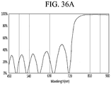
- FIG. 36 is a view illustrating a reflectivity and the number of pairs for each wavelength of a first reflection layer in a light emitting device having an infrared red wavelength according to a twelfth embodiment.
- FIGS. 37 to 43 are views illustrating a method for manufacturing the light emitting device according to the ninth embodiment.
- FIG. 44 is a cross-sectional view of a light emitting device package according to an embodiment.
- FIG. 1 is a plan view of a light emitting device according to a first embodiment
- FIG. 2 is a view illustrating a portion A of FIG. 1
- FIG. 3 is a cross-sectional view of the light emitting device, taken along line I-I′ of FIG. 1 .
- a light emitting device 100 may include a light emitting structure 110 , an upper electrode pad 174 , a branch electrode 172 , a first reflection layer 132 , and a lower electrode 140 .
- the light emitting structure 110 may be disposed on the lower electrode 140 , and the upper electrode pad 174 and the branch electrode 172 may be disposed on the light emitting structure 110 .
- the light emitting structure 110 may include a first conductive type semiconductor layer 112 , an active layer 114 disposed below the first conductive type semiconductor layer 112 , and a second conductive type semiconductor layer 116 on the active layer 114 .
- the lower ohmic pattern 141 may contact a bottom surface of the light emitting structure 110 .
- the lower ohmic pattern 141 may directly contact the light emitting structure 110 . That is, the second conductive type semiconductor layer 116 may contact the lower ohmic pattern 141 and be disposed on a top surface of the lower ohmic pattern 141 .
- the second reflection layer 142 may be provided as a single layer or a plurality of layers, which is made of a material having superior electrical contact properties and high reflectivity.
- FIG. 4 is a view illustrating results obtained by comparing luminous intensities according to Comparative examples 1 and 2 to Embodiment.
- the active layer 114 may selectively include a single quantum well structure, a multi quantum well (MQW) structure, a quantum wire structure, or a quantum dot structure.
- the active layer 114 may be made of a compound semiconductor.
- the active layer 114 may be realized by using, for example, at least one of a group-group and a group-group compound semiconductor.
- the second conductive type semiconductor layer 116 may be formed on the active layer 114 .
- the second conductive type semiconductor layer 116 may be realized by using a semiconductor compound, for example, a group-group and a group-group compound semiconductor.
- the second conductive type semiconductor layer 116 may be provided as a single layer or a multi layer.
- a second conductive type dopant may be doped into the second conductive type semiconductor layer 116 .
- the second conductive type AlGaN-based semiconductor layer 116 is a p-type semiconductor layer
- the second conductive type dopant may include Mg, Zn, Ca, Sr, or Ba as a p-type dopant.
- the upper electrode pad 174 may cover the exposed first conductive type semiconductor layer 112 and a portion of the branch electrode 172 .
- the upper electrode pad 274 may adopt the technical features of the upper electrode pad (see reference numeral 174 of FIGS. 1 to 10 ) according to the first embodiment.
- the light emitting device 101 according to the second embodiment may adopt the technical features of the light emitting device of FIGS. 1 to 10 according to the foregoing embodiment except for the structures of the first and second branch electrodes 272 a and 272 b.
- the current spreading may be improved by the first and second branch electrodes 272 a and 272 b , which are respectively connected to the first and second connection electrodes 274 p 1 and 274 p 2 protruding from the upper electrode pad 274 , and since the upper ohmic layer having bandgap energy greater than that of the active layer decreases in surface area, the light absorption by the upper ohmic layer may be reduced to improve the light loss.
- the light emitting device 102 according to the third embodiment may be improved in current spreading to reduce the light loss, thereby improving the luminous intensity.
- FIG. 13 is a cross-sectional view of a light emitting device according to a fourth embodiment.
- a light emitting device 400 may include a light emitting structure 410 , an upper electrode 470 , a first reflection layer 432 , and a lower electrode 440 .
- the light emitting structure 410 may be disposed on the lower electrode 440 and also disposed below the upper electrode 470 .
- the light emitting structure 410 may emit light having a red wavelength.
- the first conductive type semiconductor layer 412 may be made of at least one of AlGaP, InGaP, AlInGaP, InP, GaN, InN, AlN, InGaN, AlGaN, InAIGaN, AlInN, AlGaAs, InGaAs, AlInGaAs, and GaP.
- the active layer 414 may selectively include a single quantum well structure, a multi quantum well (MQW) structure, a quantum wire structure, or a quantum dot structure.
- the active layer 414 may be made of a compound semiconductor.
- the active layer 414 may be realized by using, for example, at least one of a group-group and a group-group compound semiconductor.
- the active layer 414 may include a quantum well and a quantum barrier.
- the quantum well and the quantum barrier may be alternately disposed.
- Each of the quantum well and the quantum barrier may be made of a semiconductor material having a compositional formula of InxAlyGa1-x-yP (0 ⁇ x ⁇ 1, 0 ⁇ y ⁇ 1, 0 ⁇ x+y ⁇ 1) or have a structure of one or more pairs of GaInP/AlGaInP, GaP/AlGaP, InGaP/AlGaP, InGaN/GaN, InGaN/InGaN, GaN/AlGaN, InAIGaN/GaN, GaAs/AlGaAs, and InGaAs/AlGaAs, but is not limited thereto.
- the lower electrode 440 may include an ohmic pattern 441 , a second reflection layer 442 , a bonding layer 444 , and a support substrate 446 .
- the second reflection layer 442 may be provided as a ling layer or a plurality of layers having superior electrical contact properties and high reflectivity.
- the second reflection layer 442 may be made of a material having superior electrical contact properties and high reflectivity.
- the second reflection layer 442 may be provided as a single layer or a multi layer, which is made of a metal or an alloy including at least one of Pd, Ir, Ru, Mg, Zn, Pt, Ag, Ni, Al, Rh, Au, and Hf.
- the light emitting device 400 may include first and second window semiconductor layers 420 and 160 , each of which is made of a semiconductor material.
- the first and second window semiconductor layers 420 and 160 may be made of a semiconductor material having a compositional formula of InxAlyGa1-x-yP (0 ⁇ x ⁇ 1, 0 ⁇ y ⁇ 1, 0 ⁇ x+y ⁇ 1), but is not limited thereto.
- the first and second window semiconductor layers 420 and 160 may be made of at least one of Zn, Cd, S, Se, Al, Ga, As, Te, In, and P.
- the first and second window semiconductor layers 420 and 160 may be made of a material selected from ZnSe, ZnTe, and ZnS, but is not limited thereto.
- each of the first and second window semiconductor layers 420 and 160 may be made of a material selected from InAlGaP, InAlP, GaP, and InGaP as phosphorous (P)-based semiconductors.
- the first and second window semiconductor layers 420 and 160 may have the same composition.
- the first and second window semiconductor layers 420 and 160 may have compositions different from each other.
- the first window semiconductor layer 420 may be made of a material selected from InAlGaP, InAlP, GaP, and InGaP as the phosphorous (P)-based semiconductors
- the second window semiconductor layer 460 may be made of at least one of Zn, Cd, S, Se, Al, Ga, As, Te, In, and P.
- the first and second window semiconductor layers 420 and 160 may be made of a material selected from ZnSe, ZnTe, and ZnS, but is not limited thereto.
- the first window semiconductor layer 420 may be disposed below the light emitting structure 410 .
- the first window semiconductor layer 420 may be disposed between the second conductive type semiconductor layer 416 and the lower electrode 440 to perform a current spreading function.
- the first window semiconductor layer 420 may directly contact the second conductive type semiconductor layer 416 and the lower electrode 440 .
- the first window semiconductor layer 420 may directly contact the ohmic pattern 441 and the first reflection layer 432 .
- the first window semiconductor layer 420 may be disposed between the second conductive type semiconductor layer 416 and the ohmic pattern 441 .
- the first window semiconductor layer 420 may be disposed between the first reflection layer 432 and the second conductive type semiconductor layer 416 .
- a second conductive type dopant may be doped into the first conductive type semiconductor layer 420 .
- the first window semiconductor layer 420 may include the p-type dopant.
- the first window semiconductor layer 420 may include a doping concentration greater than that of the second conductive type semiconductor layer 416 , but is not limited thereto.
- the first window semiconductor layer 420 may have a thickness greater than that of the second conductive type semiconductor layer 416 , but is not limited thereto.
- the second window semiconductor layer 460 may be disposed on the light emitting structure 410 .
- the second window semiconductor layer 460 may be disposed between the first conductive type semiconductor layer 416 and the upper electrode 470 to perform a current spreading function.
- the second window semiconductor layer 460 may directly contact the first conductive type semiconductor layer 412 and the upper electrode 470 .
- the light emitting device 400 according to the fourth embodiment is limited to the structure including the first and second window semiconductor layers 420 and 160 , the present invention is not limited thereto.
- the first window semiconductor layer 420 may be omitted.
- the light extraction structure 461 may be disposed on the second window semiconductor layer 460 to improve the light extraction efficiency.
- the current spreading effect and the light extraction efficiency may be improved to improve the luminous intensity.
- FIGS. 14 to 18 are views illustrating a method for manufacturing the light emitting device according to the fourth embodiment.
- the substrate 401 may be made of a material having high thermal conductivity. Also, the substrate 401 may be provided as a single layer or a multi layer.
- the substrate 401 may be a conductive substrate or an insulation substrate.
- the substrate 401 may be made of at least one of GaAs, sapphire (Al2O3), SiC, Si, GaN, ZnO, GaP, InP, Ge, and Ga203.
- a cleaning process may be performed on the substrate 401 before the light emitting structure 410 is formed to remove impurities on a surface of the substrate 401 .
- a buffer layer 402 may be disposed between the substrate 401 and the light emitting structure 410 .
- the buffer layer 402 may reduce a difference in lattice constant between the substrate 401 and a semiconductor layer.
- the buffer layer 402 may be made of a material selected from GaN, AlN, AlGaN, InGaN, InN, InAIGaN, AlInN, AlGaAs, GaP, GaAs, GaAsP, and AlGaInP.
- the buffer layer 402 may be an undoped GaN, but is not limited thereto.
- the first window semiconductor layer 420 may have a thickness greater than that of the second conductive type semiconductor layer 416 , but is not limited thereto.
- a first reflection layer 432 and an ohmic pattern 441 may be formed on the first window semiconductor layer 420 .
- the ohmic pattern 441 may be made of a material having superior electrical contact properties with respect to the semiconductor. Also, the ohmic pattern 441 may be provided as a single layer or a multi layer.
- the ohmic pattern 441 may include at least one of Ag, Ni, Cr, Ti, Al, Rh, Pd, Ir, Ru, Mg, Zn, Pt, Au, Hf, Be, indium tin oxide (ITO), indium zinc oxide (IZO), indium zinc tin oxide (IZTO), indium aluminum zinc oxide (IAZO), indium gallium zinc oxide (IGZO), indium gallium tin oxide (IGTO), aluminum zinc oxide (AZO), antimony tin oxide (ATO), gallium zinc oxide (GZO), IZON (IZO Nitride), AGZO (Al—Ga ZnO), IGZO (In—Ga ZnO), ZnO, IrOx, RuOx, NiO, RuOx/ITO, Ni/I
- the ohmic pattern 441 may directly contact the first window semiconductor layer 420 .
- a separate reflection layer (not shown) may be formed between the ohmic pattern 441 and the first window semiconductor layer 420 .
- the ohmic pattern 441 may be disposed on the same plane as the first reflection layer 432 .
- the is, top surfaces and bottom surfaces of the ohmic pattern 441 and the first reflection layer 432 may be disposed on the same plane, but are not limited thereto.
- a second reflection layer 442 , a bonding layer 444 , and a support substrate 446 may be formed on the ohmic pattern 441 and the first reflection layer 432 .
- the second reflection layer 442 may be provided as a single layer or a multi layer.
- the second reflection layer 442 may be made of a material having superior electrical contact properties and high reflectivity.
- the second reflection layer 442 may be provided as a single layer or a multi layer, which is made of a metal or an alloy including at least one of Pd, Ir, Ru, Mg, Zn, Pt, Ag, Ni, Al, Rh, Au, and Hf.
- the bonding layer 444 may be provided as a single layer or a multi layer. Also, the bonding layer 444 may be made of a material having superior electrical contact properties. For example, the bonding layer 444 may be made of Ni, Ti, Au, or an alloy thereof, but is not limited thereto.
- the support substrate 446 may be provided as a single layer or a multi layer. Also, the support substrate 446 may be made of a material having superior electrical contact properties. For example, the support substrate 446 may selectively include a carrier wafer (e.g., GaN, Si, Ge, GaAs, ZnO, SiGe, SiC, etc), Cu, Au, Cu Alloy, Ni, Cu—W, and the like.
- a carrier wafer e.g., GaN, Si, Ge, GaAs, ZnO, SiGe, SiC, etc
- Cu Au
- Cu Alloy Ni
- Cu—W and the like.
- the substrate may be removed.
- the substrate may be removed through laser, chemical etching, or physical etching.
- the substrate may be removed through a laser lift-off method.
- energy may be applied to an interface between the substrate (see reference numeral 101 of FIG. 14 ) and the light emitting structure 410 to allow a bonded surface of the light emitting structure 410 to be pyrolyzed, thereby separating the substrate 401 from the light emitting structure 410 .
- the first conductive type semiconductor layer 412 may be exposed from the outside.
- the second window semiconductor layer 460 may be disposed on the first conductive type semiconductor layer 412 to perform a current spreading function.
- the second window semiconductor layer 460 may directly contact the first conductive type semiconductor layer 412 .
- the second window semiconductor layer 460 may be formed by using a method such as chemical vapor deposition (CVD), molecular beam epitaxy (MBE), sputtering, or hydride vapor phase epitaxy (HVPE), but is not limited thereto.
- CVD chemical vapor deposition
- MBE molecular beam epitaxy
- HVPE hydride vapor phase epitaxy
- a first conductive type dopant may be doped into the second conductive type semiconductor layer 460 .
- the second window semiconductor layer 460 may include the n-type dopant.
- the second window semiconductor layer 460 may include a doping concentration greater than that of the first conductive type semiconductor layer 412 , but is not limited thereto.
- the second window semiconductor layer 460 may have a thickness greater than that of the first conductive type semiconductor layer 412 , but is not limited thereto.
- the second window semiconductor layer 460 may has a thickness of 3 ⁇ m or more.
- the second window semiconductor layer 460 may has a thickness of 3 ⁇ m to 100 ⁇ m.
- the thickness of the second window semiconductor layer 460 is less than 3 ⁇ m, the current spreading effect may be deteriorated.
- the thickness of the second window semiconductor layer 460 exceeds 100 ⁇ m, light extraction efficiency may be deteriorated due to the thick thickness, and an operation voltage VF 3 may increase.
- the second window semiconductor layer 460 may have a light extraction structure 461 having a roughness shape on a top surface thereof.
- the light extraction structure 461 may be regular, but is not limited thereto.
- the light extraction structure 461 may be irregular and disposed on a portion of the top surface of the second window semiconductor layer 460 .
- the light extraction structure 461 may have a circular shape, an oval shape, or a polygonal shape, but is not limited thereto.
- the light extraction structure 461 may be disposed on an area except for an area overlapping the upper electrode 470 , but is not limited thereto.
- the light extraction structure 461 may be disposed on the area overlapping the upper electrode 470 .
- the light extraction structure 461 may have a function of improving external extraction efficiency of light incident into the second window semiconductor layer 460 .
- the upper electrode 470 may be formed on the second window semiconductor layer 460 .
- the upper electrode 470 may include an ohmic layer (not shown), a branch electrode (not shown), and an upper electrode pad (not shown), but is not limited thereto.
- the upper electrode 470 may be provided as a single layer or a multi layer and be made of at least one of Ti, Cr, Ni, Al, Pt, Au, W, Cu, Mo, and Cu—W, but is not limited thereto.
- the present invention is not limited thereto.
- the order of the manufacturing processes may be changed.
- the first window semiconductor layer 420 may be disposed between the light emitting structure 410 and the lower electrode 440
- the second window semiconductor layer 460 may be disposed between the light emitting structure 410 and the upper electrode to improve the current spreading effect.
- the light extraction structure 461 may be disposed on the second window semiconductor layer 460 to improve the light extraction efficiency.
- the current spreading effect and the light extraction efficiency may be improved to improve the luminous intensity.
- a light emitting device 500 may include a light emitting structure 510 , an upper electrode pad 574 , a branch electrode 572 , a first reflection layer 530 , a window layer 520 , and a lower electrode 540 .
- the light emitting structure 510 may be disposed on the lower electrode 540 , and the upper electrode pad 574 and the branch electrode 572 may be disposed on the light emitting structure 510 .
- the first conductive type semiconductor layer 512 may be realized by using a semiconductor compound, for example, a group-group and a compound semiconductor such as a group-group.
- the first conductive type semiconductor layer 512 may be provided as a single layer or a multi layer.
- a first conductive type dopant may be doped into the first conductive type semiconductor layer 512 .
- the first conductive type semiconductor layer 512 is an n-type semiconductor layer
- an n-type dopant may be doped.
- the n-type dopant may include Si, Ge, Sn, Se, and Te, but is not limited thereto.
- the first conductive type semiconductor layer 512 may be made of at least one of AlGaP, InGaP, AlInGaP, InP, GaN, InN, AlN, InGaN, AlGaN, InAIGaN, AlInN, AlGaAs, InGaAs, AlInGaAs, and GaP.
- the active layer 514 may selectively include a single quantum well structure, a multi quantum well (MQW) structure, a quantum wire structure, or a quantum dot structure.
- the active layer 514 may be made of a compound semiconductor.
- the active layer 514 may be realized by using, for example, at least one of a group-group and a group-group compound semiconductor.
- the active layer 514 may include a quantum well and a quantum barrier.
- the quantum well and the quantum barrier may be alternately disposed.
- Each of the quantum well and the quantum barrier may be made of a semiconductor material having a compositional formula of InxAlyGa1-x-yP (0 ⁇ x ⁇ 1, 0 ⁇ y ⁇ 1, 0 ⁇ x+y ⁇ 1) or have a structure of one or more pairs of GaInP/AlGaInP, GaP/AlGaP, InGaP/AlGaP, InGaN/GaN, InGaN/InGaN, GaN/AlGaN, InAIGaN/GaN, GaAs/AlGaAs, and InGaAs/AlGaAs, but is not limited thereto.
- the second conductive type semiconductor layer 516 may be formed on the active layer 514 .
- the second conductive type semiconductor layer 516 may be realized by using a semiconductor compound, for example, a group-group and a group-group compound semiconductor.
- the second conductive type semiconductor layer 516 may be provided as a single layer or a multi layer.
- a second conductive type dopant may be doped into the second conductive type semiconductor layer 516 .
- the second conductive type semiconductor layer 516 may be made of at least one of AlGaP, InGaP, AlInGaP, InP, GaN, InN, AlN, InGaN, AlGaN, InAIGaN, AlInN, AlGaAs, InGaAs, AlInGaAs, and GaP.
- the second conductive type semiconductor layer 516 is a p-type semiconductor layer
- the second conductive type dopant may include Mg, Zn, Ca, Sr, or Ba as a p-type dopant.
- the window layer 520 may be disposed below the light emitting structure 510 .
- the window layer 520 may be disposed between the second conductive type semiconductor layer 516 and the lower electrode 540 to perform a current spreading function.
- the window layer 520 may be disposed between the second conductive type semiconductor layer 516 and first and second lower ohmic patterns 541 a and 141 b .
- the window layer 520 may be disposed between the first reflection layer 530 and the second conductive type semiconductor layer 516 .
- the window layer 520 may directly contact the second conductive type semiconductor layer 516 and the lower electrode 540 .
- the window layer 520 may have a bottom surface directly contacting a top surface of the first reflection layer 530 and top surfaces of the first and second lower ohmic patterns 541 a and 141 b.
- the window layer 520 may include a second conductive type dopant.
- the window layer 520 may include the p-type dopant.
- the window layer 520 may include a doping concentration greater than that of the second conductive type semiconductor layer 516 , but is not limited thereto.
- the window layer 520 may have a thickness greater than that of the second conductive type semiconductor layer 516 , but is not limited thereto.
- An edge of the window layer 520 may be exposed to the outside.
- the edge of the window layer 520 may include top and outer surfaces of the light emitting structure 510 , which are exposed outward, but is not limited thereto.
- the lower electrode 540 may include a second reflection layer 542 , a bonding layer 544 , a support substrate 546 , and first and second lower ohmic patterns 541 a and 141 b.
- the first and second lower ohmic patterns 541 a and 141 b may be disposed below the light emitting structure 510 .
- the first and second lower ohmic patterns 541 a and 141 b may be disposed on a lower portion of the window layer 520 disposed below the light emitting structure 500 .
- the first and second lower ohmic patterns 541 a and 141 b may directly contact the window layer 520 .
- the first lower ohmic pattern 541 a may be disposed along the edge of the window layer 520 .
- the first lower ohmic pattern 541 a may not vertically overlap the active layer 514 .
- the first lower ohmic pattern 541 a may be disposed on an area that vertically overlaps a top surface of the edge of the window layer 520 , which is exposed from the light emitting structure 510 .
- the second lower ohmic pattern 541 b may vertically overlap the light emitting structure 510 .
- the second lower ohmic pattern 541 b may vertically overlap the active layer 513 .
- the second lower ohmic pattern 541 b may have a circular shape, an oval shape, or a polygonal shape when viewed from an upper side, but is not limited thereto.
- the second lower ohmic pattern 541 b may have a surface area less than 4.0% of an area of the first reflection layer 530 within the area vertically overlapping the active layer 514 .
- the second lower ohmic pattern 541 b having the surface area less than 4.0% of the area of the first reflection layer 530 within the area vertically overlapping the active layer 514 may improve a luminous flux of the light emitting device 500 and also improve rising of an operation voltage VF.
- the second lower ohmic pattern 541 b may have a surface area corresponding to 0.6% to 4.0% of the area of the first reflection layer 530 within the area vertically overlapping the active layer 514 , but is not limited thereto.
- the second lower ohmic pattern 541 b may have a surface area corresponding to 1.4% of the area of the first reflection layer 530 within the area vertically overlapping the active layer 514 , but is not limited thereto.
- the ohmic contact area between the second lower ohmic pattern 541 b and the window layer 520 may be reduced to increase in operation voltage VF.
- the second lower ohmic pattern 541 b may have a surface area exceeding 4.0% the surface area of the first reflection layer 530 within the area vertically overlapping the active layer 514 , the luminous flux may be deteriorated.
- the second lower ohmic pattern 541 b may not vertically overlap the upper electrode pad 574 and the branch electrode 572 .
- the second lower ohmic pattern 541 b vertically overlaps the upper electrode pad 574 and the branch electrode 572 , since each of distances between the second lower ohmic pattern 541 , the upper electrode pad 574 , and the branch electrode 572 are minimized on the vertically overlapping area, current crowding may occur on the vertically overlapping area.
- the current crowding may cause droop of light according to a driving time of the light emitting device due to coupling of electrons and holes in a local area.
- the upper electrode pad 574 , the branch electrode 572 , and the second lower ohmic pattern 541 b may not overlap each other to improve the current crowding and the droop of the light.
- the first lower ohmic pattern 541 a may be disposed to vertically overlap the edge of the window layer 520 .
- the first lower ohmic pattern 541 a may be disposed to vertically overlap the edge of the window layer 520 to increase an ohmic contact area with the window layer 520 .
- the first lower ohmic pattern 541 a may be disposed to vertically overlap the edge of the window layer 520 to increase the contact area with the window layer 520 , thereby improving the operation voltage VF and electrical properties such as the current spreading.
- the first lower ohmic pattern 541 a may vertically overlap the edge of the window layer 520 along the outside of the light emitting structure 510 and may not vertically overlap the edge of the light emitting structure 510 , but are not limited thereto.
- the first and second lower ohmic patterns 541 a and 141 b may be made of a material having superior electrical contact with the semiconductor. Also, each of the first and second lower ohmic patterns 541 a and 141 b may be provided as a single layer or a multi layer.
- Each of the first and second lower ohmic patterns 541 a and 141 b may include at least one of Ag, Ni, Cr, Ti, Al, Rh, Pd, Ir, Ru, Mg, Zn, Pt, Au, Hf, Be, Ge, indium tin oxide (ITO), indium zinc oxide (IZO), indium zinc tin oxide (IZTO), indium aluminum zinc oxide (IAZO), indium gallium zinc oxide (IGZO), indium gallium tin oxide (IGTO), aluminum zinc oxide (AZO), antimony tin oxide (ATO), gallium zinc oxide (GZO), IZON (IZO Nitride), AGZO (Al—Ga ZnO), IGZO (In—Ga ZnO), ZnO, IrOx, RuOx, NiO, RuOx/ITO, Ni/IrOx/Au, and Ni/IrOx/Au/ITO, but is not limited to the above-described materials.
- the second reflection layer 542 may be provided as a single layer or a plurality of layers.
- the second reflection layer 542 may be made of a material having superior electrical contact properties and high reflectivity.
- the second reflection layer 542 may be provided as a single layer or a multi layer, which is made of a metal or an alloy including at least one of Pd, Ir, Ru, Mg, Zn, Pt, Ag, Ni, Al, Rh, Au, Ti, Hf, and ITO.
- Each of the bonding layer 544 and the support substrate 546 may be provided as a single layer or a plurality of layers.
- the bonding layer 544 may be provided as a single layer or a multi layer and be made of at least one of Ni, Ti, Cr, Pt. Au, Sn, In, Pd, Cu, and TiW, but is not limited to the above-described materials.
- the support substrate 546 may be made of a material having superior electrical contact properties.
- the support substrate 546 may selectively include a carrier wafer (e.g., GaN, Si, Ge, GaAs, ZnO, SiGe, SiC, etc), Cu, Au, Cu Alloy, Ni, Cu—W, and the like.
- the first reflection layer 530 may be disposed on the same plane as the first and second lower ohmic patterns 541 a and 141 b and include at least one metal layer (not shown) and at least one insulation layer (not shown), but is not limited thereto.
- the reflection layer 530 may be made of an insulation material having transmittance of 90% or more.
- the first reflection layer 530 may be an omni directional reflector (ODR), but is not limited thereto.
- the first reflection layer 530 may be provided as a single layer or a multi layer and made of at least one of SiO2, SiN, Al2O3, ZnO, and ITO, but is not limited thereto.
- the first reflection layer 530 may be disposed on the same plane as the first and second lower ohmic patterns 541 a and 141 b .
- the first reflection layer 530 may be disposed in parallel to the first and second lower ohmic patterns 541 a and 141 b .
- the second lower ohmic patterns 541 b may be spaced apart from each other in a dot shape.
- the first reflection layer 530 may have a diameter or a horizontal width, which is greater than a width of the second lower ohmic pattern 541 b disposed between the first reflection layers 530 , but is not limited thereto.
- the first reflection layer 530 may have the same thickness as each of the first and second lower ohmic patterns 541 a and 141 b , but is not limited thereto.
- the first reflection layer 530 may directly contact a bottom surface of the window layer 520 , but is not limited thereto.
- the light emitting device 500 may include an upper electrode pad 574 and a branch electrode 572 . At least one or more of the upper electrode pad 574 and the branch electrode 572 may be disposed, but is not limited thereto.
- a conductive layer 571 may be disposed between the first conductive type semiconductor layer 512 and the branch electrode 572 .
- the conductive layer 571 may be disposed below the branch electrode 572 .
- the conductive layer 571 may be provided as a single layer or a plurality of layers, which is made of a material having superior electrical contact with the semiconductor.
- the conductive layer 571 may include at least one of Ag, Ni, Cr, Ti, Al, Rh, Pd, Ir, Ru, Mg, Zn, Pt, Au, Hf, Be, Ge, indium tin oxide (ITO), indium zinc oxide (IZO), indium zinc tin oxide (IZTO), indium aluminum zinc oxide (IAZO), indium gallium zinc oxide (IGZO), indium gallium tin oxide (IGTO), aluminum zinc oxide (AZO), antimony tin oxide (ATO), gallium zinc oxide (GZO), IZON (IZO Nitride), AGZO (Al—Ga ZnO), IGZO (In—Ga ZnO), ZnO, IrOx, RuOx, NiO, RuOx/ITO, Ni/IrOx/Au, and Ni/IrOx/Au/ITO, but is not limited to the above-described materials.
- the upper electrode pad 574 may be disposed at a central area of the light emitting device 510 , but is not limited thereto.
- the upper electrode pad 574 may be disposed on at least one edge of the light emitting structure 510 .
- the upper electrode pad 574 may be disposed on a top surface of the first conductive type semiconductor layer 512 .
- the upper electrode pad 574 may directly contact the first conductive type semiconductor layer 512 .
- the upper electrode pad 574 may come into schottky contact with the first conductive type semiconductor layer 512 , and the branch electrode 572 and the conductive layer 571 may come into ohmic contact with the first conductive type semiconductor layer 512 .
- the schottky contact may occur between the upper electrode pad 574 and the first conductive type semiconductor layer 512 to control current through a potential barrier of a junction part due to reverse bias.
- a current spreading effect may be generally improved to improve a light output.
- FIG. 21 is a graph illustrating an operation voltage according to a surface area of the second lower ohmic pattern
- FIG. 22 is a graph illustrating a luminous flux according to the area of the second lower ohmic pattern.
- the luminous flux of the light emitting device may be improved by the second lower ohmic pattern having the surface area corresponding to 4.0% or less of that of the first reflection layer within the area vertically overlapping the active layer, and simultaneously, the rising of the operation voltage VF may be improved.
- the second lower ohmic pattern according to an embodiment may have a surface area corresponding to 0.6% to 4.0% of the surface area of the first reflection layer within the area vertically overlapping the active layer, but is not limited thereto.
- the substrate 501 may be made of a material having high thermal conductivity. Also, the substrate 501 may be provided as a single layer or a multi layer.
- the substrate 501 may be a conductive substrate or an insulation substrate.
- the substrate 501 may be made of at least one of GaAs, sapphire (Al2O3), SiC, Si, GaN, ZnO, GaP, InP, Ge, and Ga203.
- a cleaning process may be performed on the substrate 501 before the light emitting structure 510 is formed to remove impurities on a surface of the substrate 401 .
- a buffer layer 501 may be disposed between the substrate 502 and the light emitting structure 510 .
- the light emitting structure 510 may include a first conductive type semiconductor layer 512 , an active layer 514 formed on the first conductive type semiconductor layer 512 , and a second conductive type semiconductor layer 516 formed on the active layer 514 .
- the first conductive type semiconductor layer 512 may be realized by using a semiconductor compound, for example, a group-group and a compound semiconductor such as a group-group.
- the first conductive type semiconductor layer 512 may be provided as a single layer or a multi layer.
- a first conductive type dopant may be doped into the first conductive type semiconductor layer 512 .
- the first conductive type semiconductor layer 512 is an n-type semiconductor layer
- an n-type dopant may be doped.
- the n-type dopant may include Si, Ge, Sn, Se, and Te, but is not limited thereto.
- the first conductive type semiconductor layer 512 may include a semiconductor material having a compositional formula of InxAlyGa1-x-yP (0 ⁇ x ⁇ 1, 0 ⁇ y ⁇ 1, 0 ⁇ x+y ⁇ 1), but is not limited thereto.
- the first conductive type semiconductor layer 512 may be made of at least one of AlGaP, InGaP, AlInGaP, InP, GaN, InN, AlN, InGaN, AlGaN, InAIGaN, AlInN, AlGaAs, InGaAs, AlInGaAs, and GaP.
- a light extraction pattern 519 having a plurality of concave portions and a plurality of convex portions to form a roughness shape may be formed on the surface of the first conductive type semiconductor layer 512 .
- the first conductive type semiconductor layer 512 may be formed by using a method such as chemical vapor deposition (CVD), molecular beam epitaxy (MBE), sputtering, or hydride vapor phase epitaxy (HVPE), but is not limited thereto.
- CVD chemical vapor deposition
- MBE molecular beam epitaxy
- HVPE hydride vapor phase epitaxy
- the active layer 514 may be formed on the first conductive type semiconductor layer 512 .
- the active layer 514 may selectively include a single quantum well structure, a multi quantum well (MQW) structure, a quantum wire structure, or a quantum dot structure.
- the active layer 514 may be made of a compound semiconductor.
- the active layer 514 may be realized by using, for example, at least one of a group-group and a group-group compound semiconductor.
- the active layer 514 may include a quantum well and a quantum barrier.
- the active layer 514 may have a structure of one or more pairs of GaInP/AlGaInP, GaP/AlGaP, InGaP/AlGaP, InGaN/GaN, InGaN/InGaN, GaN/AlGaN, InAIGaN/GaN, GaAs/AlGaAs, and InGaAs/AlGaAs, but is not limited thereto.
- the second conductive type semiconductor layer 516 may be formed on the active layer 514 .
- the second conductive type semiconductor layer 516 may be realized by using a semiconductor compound, for example, a group-group and a group-group compound semiconductor.
- the second conductive type semiconductor layer 516 may be provided as a single layer or a multi layer.
- a second conductive type dopant may be doped into the second conductive type semiconductor layer 516 .
- the second conductive type dopant may include Mg, Zn, Ca, Sr, or Ba as a p-type dopant.
- the second conductive type semiconductor layer 516 may include a semiconductor material having a compositional formula of InxAlyGa1-x-yP (0 ⁇ x ⁇ 1, 0 ⁇ y ⁇ 1, 0 ⁇ x+y ⁇ 1).
- the first conductive type semiconductor layer 512 may be made of at least one of AlGaP, InGaP, AlInGaP, InP, GaN, InN, AlN, InGaN, AlGaN, InAIGaN, AlInN, AlGaAs, InGaAs, AlInGaAs, and GaP.
- the second conductive type semiconductor layer 516 may be formed by using a method such as chemical vapor deposition (CVD), molecular beam epitaxy (MBE), sputtering, or hydride vapor phase epitaxy (HVPE), but is not limited thereto.
- CVD chemical vapor deposition
- MBE molecular beam epitaxy
- HVPE hydride vapor phase epitaxy
- the first window semiconductor layer 420 when the first window semiconductor layer 420 includes Zn, the first window semiconductor layer 420 may be made of a material selected from ZnSe, ZnTe, and ZnS, but is not limited thereto.
- the window layer 520 may be made of a material selected from InAlGaP, InAlP, GaP, and InGaP as phosphorous (P)-based semiconductors.
- the window layer 520 may be formed by using a method such as chemical vapor deposition (CVD), molecular beam epitaxy (MBE), sputtering, or hydride vapor phase epitaxy (HVPE), but is not limited thereto.
- CVD chemical vapor deposition
- MBE molecular beam epitaxy
- HVPE hydride vapor phase epitaxy
- the window layer 520 may include a second conductive type dopant.
- the window layer 520 may include the p-type dopant.
- the window layer 520 may include a doping concentration greater than that of the second conductive type semiconductor layer 516 , but is not limited thereto.
- the window layer 520 may have a thickness greater than that of the second conductive type semiconductor layer 516 , but is not limited thereto.
- the first reflection layer 530 may be deposited on the window layer 520 and include a plurality of holes 531 , through which the window layer 520 is exposed, formed through an etching process using photoresist.
- the first and second lower ohmic patterns 541 a and 141 b may be deposited on the plurality of holes 531 , but is not limited thereto.
- the first reflection layer 530 may be disposed on the same plane as the first and second lower ohmic patterns 541 a and 141 b and include at least one metal layer (not shown) and at least one insulation layer (not shown), but is not limited thereto.
- the reflection layer 530 may be made of an insulation material having transmittance of 90% or more.
- the first reflection layer 530 may be an omni directional reflector (ODR), but is not limited thereto.
- the first reflection layer 530 may be made of at least one of SiO2, SiN, Al2O3, ZnO, and ITO, but is not limited thereto.
- the first reflection layer 530 may be disposed on the same plane as the first and second lower ohmic patterns 541 a and 141 b .
- the first reflection layer 530 may be disposed in parallel to the first and second lower ohmic patterns 541 a and 141 b .
- the first and second lower ohmic patterns 541 b and 141 b may be spaced apart from each other in a dot shape.
- the first reflection layer 530 may have a diameter or a horizontal width, which is greater than a width of the second lower ohmic pattern 541 b disposed between the first reflection layers 530 , but is not limited thereto.
- the first reflection layer 530 may have the same thickness as each of the first and second lower ohmic patterns 541 a and 141 b , but is not limited thereto.
- the first reflection layer 530 may directly contact a bottom surface of the window layer 520 , but is not limited thereto.
- the first and second lower ohmic patterns 541 a and 141 b may be made of a material having superior electrical contact with the semiconductor. Also, each of the first and second lower ohmic patterns 541 a and 141 b may be provided as a single layer or a multi layer.
- Each of the first and second lower ohmic patterns 541 a and 141 b may include at least one of Ag, Ni, Cr, Ti, Al, Rh, Pd, Ir, Ru, Mg, Zn, Pt, Au, Hf, Be, Ge, indium tin oxide (ITO), indium zinc oxide (IZO), indium zinc tin oxide (IZTO), indium aluminum zinc oxide (IAZO), indium gallium zinc oxide (IGZO), indium gallium tin oxide (IGTO), aluminum zinc oxide (AZO), antimony tin oxide (ATO), gallium zinc oxide (GZO), IZON (IZO Nitride), AGZO (Al—Ga ZnO), IGZO (In—Ga ZnO), ZnO, IrOx, RuOx, NiO, RuOx/ITO, Ni/IrOx/Au, and Ni/IrOx/Au/ITO, but is not limited to the above-described materials.
- the first and second lower ohmic patterns 541 a and 141 b may directly contact the window layer 520 and the second conductive type semiconductor layer 516 .
- a separate reflection layer (not shown) may be formed between the first and second lower ohmic patterns 541 a and 141 b and the second conductive type semiconductor layer 516 .
- the first lower ohmic pattern 541 a may be disposed along the edge of the window layer 520 .
- the first lower ohmic pattern 541 a may not vertically overlap the active layer 514 .
- the first lower ohmic pattern 541 a may vertically overlap a top surface of the edge of the window layer 520 , which is exposed from the light emitting structure 510 .
- the second lower ohmic pattern 541 b may vertically overlap the light emitting structure 510 .
- the second lower ohmic pattern 541 b may vertically overlap the active layer 513 .
- Each of the first and second lower ohmic patterns 541 a and 141 b may have a circular shape, an oval shape, or a polygonal shape when viewed from an upper side, but is not limited thereto.
- the second lower ohmic pattern 541 b may have a surface area less than 4.0% of an area of the first reflection layer 530 within the area vertically overlapping the active layer 514 .
- the second lower ohmic pattern 541 b having the surface area less than 4.0% of the surface area of the first reflection layer 530 may improve a luminous intensity of the light emitting device 500 and also improve rising of an operation voltage VF.
- the second lower ohmic pattern 541 b may have a surface area corresponding to 0.6% to 4.0% of the surface area of the first reflection layer 530 within the area vertically overlapping the active layer 514 , but is not limited thereto.
- the lower ohmic pattern 541 may have a surface area corresponding to 1.4% of the surface area of the first reflection layer 530 within the area vertically overlapping the active layer 514 , but is not limited thereto.
- the ohmic contact area between the second lower ohmic pattern 541 b and the window layer 520 may be reduced to increase in operation voltage VF.
- the second lower ohmic pattern 541 b may have a surface area exceeding 4.0% the surface area of the first reflection layer 530 within the area vertically overlapping the active layer 514 , the luminous flux may be deteriorated.
- a lower electrode 540 may be formed on the light emitting structure 510 .
- the lower electrode 540 may include the constituents of the first and second lower ohmic patterns 541 a and 141 b , but is not limited thereto.
- the lower electrode 540 may include a second reflection layer 542 , a bonding layer 544 , and a support substrate 546 .
- the bonding layer 544 and the support substrate 546 may be provided as a single layer or a plurality of layers.
- the bonding layer 544 may be made of at least one of Ni, Ti, Cr, Pt. Au, Sn, In, Pd, Cu, and TiW, but is not limited to the above-described materials.
- the support substrate 546 may be made of a material having superior electrical contact properties.
- the support substrate 546 may selectively include a carrier wafer (e.g., GaN, Si, Ge, GaAs, ZnO, SiGe, SiC, etc), Cu, Au, Cu Alloy, Ni, Cu—W, and the like.
- the substrate may be removed.
- the substrate may be removed through laser, chemical etching, or physical etching.
- the substrate may be removed through a laser lift-off method.
- energy may be applied to an interface between the substrate (see reference numeral 101 of FIG. 26 ) and the light emitting structure 510 to allow a bonded surface of the light emitting structure 510 to be pyrolyzed, thereby separating the substrate 502 from the light emitting structure 510 .
- the upper electrode pad 574 and the branch electrode 572 may be formed on the first conductive type semiconductor layer 512 .
- a conductive layer 571 may be disposed below the branch electrode 572 .
- the conductive layer 571 may be deposited on the first conductive type semiconductor layer 512
- the branch electrode 572 may be deposited on the conductive layer 571 . That is, the conductive layer 571 may be disposed between the first conductive type semiconductor layer 512 and the branch electrode 572 .
- the conductive layer 571 may be provided as a single layer or a multi layer. Also, the conductive layer 571 may be made of a material having superior electrical contact properties with respect to the semiconductor.
- the conductive layer 571 may include at least one of Ag, Ni, Cr, Ti, Al, Rh, Pd, Ir, Ru, Mg, Zn, Pt, Au, Hf, Be, Ge, indium tin oxide (ITO), indium zinc oxide (IZO), indium zinc tin oxide (IZTO), indium aluminum zinc oxide (IAZO), indium gallium zinc oxide (IGZO), indium gallium tin oxide (IGTO), aluminum zinc oxide (AZO), antimony tin oxide (ATO), gallium zinc oxide (GZO), IZON (IZO Nitride), AGZO (Al—Ga ZnO), IGZO (In—Ga ZnO), ZnO, IrOx, RuOx, NiO, RuOx/ITO, Ni/IrOx/
- the upper electrode pad 574 and the branch electrode 572 may be made of the same material.
- Each of the upper electrode pad 574 and the branch electrode 572 may be provided as a single layer or a plurality of layers and also be made of at least one of Ti, Cr, Ni, Al, Pt, Au, W, Cu, Mo, Cu—W, Be, Zn, and Ge, but is not limited thereto.
- the second lower ohmic pattern 541 b may have a surface area less than 4.0% of a surface area of the first reflection layer 530 within the area vertically overlapping the active layer 514 .
- the second lower ohmic pattern 541 b having the surface area less than 4.0% of the surface area of the first reflection layer 530 may improve a luminous flux of the light emitting device 500 and also improve rising of an operation voltage VF.
- the second lower ohmic pattern 541 b may have a surface area corresponding to 0.6% to 4.0% of the surface area of the first reflection layer 530 within the area vertically overlapping the active layer 514 , but is not limited thereto.
- the second lower ohmic pattern 541 b may have a surface area corresponding to 1.4% of the surface area of the first reflection layer 530 within the area vertically overlapping the active layer 514 .
- FIG. 29 is a plan view of a light emitting device according to a sixth embodiment.
- the conductive layer 671 may be disposed below the upper electrode pad 674 and the branch electrode 672 .
- the conductive layer 671 may directly contact a first conductive type semiconductor layer 512 .
- the conductive layer 671 may be provided as a single layer or a plurality of layers, which is made of a material having superior electrical contact with the semiconductor.
- Each of the upper electrode pad 674 and the branch electrode 672 may be provided as a single layer or a plurality of layers and also be made of at least one of Ti, Cr, Ni, Al, Pt, Au, W, Cu, Mo, Cu—W, Be, Zn, and Ge, but is not limited thereto.
- the upper electrode pad 674 and the branch electrode 672 may be made of materials different from each other.
- the upper electrode pad 674 may be made of a material having resistance greater than that of the branch electrode 672 .
- the upper electrode pad 674 may include Cr, and the branch electrode 672 may not include Cr.
- the upper electrode pad 674 may be made of a material having resistance greater than that of the branch electrode 672 .
- resistance between the upper electrode pad 674 and the conductive layer 671 may be greater than that between the branch electrode 672 and the conductive layer 671 . That is, since the branch electrode 672 has resistance less than that of the upper electrode pad 674 , current may flow to the conductive layer 671 through the branch electrode 672 rather than the upper electrode pad 674 . Thus, in the light emitting device according to the sixth embodiment, the current is induced to flow from the upper electrode pad 674 having the resistance greater than that of the branch electrode 672 to the branch electrode 672 , the current spreading effect may be generally improved to improve the light output.
- FIG. 30 is a plan view of a light emitting device according to a seventh embodiment.
- a light emitting device 502 may include a conductive layer 771 , an upper electrode pad 774 , and a branch electrode 772 on a light emitting structure 510 .
- a light emitting device 502 according to another embodiment may include a first reflection layer 530 and a lower electrode 540 below the light emitting structure 510 .
- the light emitting structure 510 , the first reflection layer 530 , and the lower electrode 540 may adopt the technical features of the light emitting device 500 of FIGS. 19 to 22 according to the fifth embodiment.
- the conductive layer 771 may be disposed below the branch electrode 772 .
- the conductive layer 771 may directly contact a first conductive type semiconductor layer 512 .
- the conductive layer 771 may be provided as a single layer or a plurality of layers, which is made of a material having superior electrical contact with the semiconductor.
- the conductive layer 771 may include at least one of Ag, Ni, Cr, Ti, Al, Rh, Pd, Ir, Ru, Mg, Zn, Pt, Au, Hf, Be, Ge, indium tin oxide (ITO), indium zinc oxide (IZO), indium zinc tin oxide (IZTO), indium aluminum zinc oxide (IAZO), indium gallium zinc oxide (IGZO), indium gallium tin oxide (IGTO), aluminum zinc oxide (AZO), antimony tin oxide (ATO), gallium zinc oxide (GZO), IZON (IZO Nitride), AGZO (Al—Ga ZnO), IGZO (In—Ga ZnO), ZnO, IrOx, RuOx, NiO, RuOx/ITO, Ni/IrOx/Au, and Ni/IrOx/Au/ITO, but is not limited to the above-described materials.
- the upper electrode pad 774 may be disposed at a central area of the light emitting device 510 , but is not limited thereto.
- the upper electrode pad 774 may be disposed on at least one edge of the light emitting structure 510 .
- the upper electrode pad 774 may be disposed on the light emitting structure 510 .
- the upper electrode pad 774 may directly contact the first conductive type semiconductor layer 512 .
- the upper electrode pad 774 may come into schottky contact with the first conductive type semiconductor layer 512 .
- current may be controlled between the upper electrode pad 774 and the first conductive type semiconductor layer 512 through a potential barrier of a junction part due to reverse bias.
- Each of the upper electrode pad 774 and the branch electrode 772 may be provided as a single layer or a plurality of layers and also be made of at least one of Ti, Cr, Ni, Al, Pt, Au, W, Cu, Mo, Cu—W, Be, Zn, and Ge, but is not limited thereto.
- the upper electrode pad 774 and the branch electrode 772 may be made of materials different from each other.
- the upper electrode pad 774 may be made of a material having resistance greater than that of the branch electrode 772 .
- the upper electrode pad 774 may include Cr, and the branch electrode 772 may not include Cr.
- the upper electrode pad 774 may come into schottky contact with the first conductive type semiconductor layer 512 , and the conductive layer 771 may be disposed below the branch electrode 772 to maintain the state in which the current flows through the branch electrode 772 . Furthermore, the current may be induced to flow through the branch electrode 772 by the upper electrode pad 774 having the resistance greater than that of the branch electrode 772 to more improve the current spreading effect when compared to the light emitting device according to the sixth embodiment.
- FIG. 31 is a plan view of a light emitting device according to an eighth embodiment
- FIG. 32 is a cross-sectional view of the light emitting device, taken along line III-III′ of FIG. 31 .
- a light emitting device may include a light emitting structure 810 , an upper electrode pad 874 , a branch electrode 872 , a window layer 820 , a distributed bragg reflector 130 , a first reflection layer 830 , and a lower electrode 840 .
- the light emitting structure 810 may be disposed on the lower electrode 840 , and the upper electrode pad 874 and the branch electrode 872 may be disposed on the light emitting structure 810 .
- the light emitting structure 810 may include a first conductive type semiconductor layer 812 , an active layer 814 disposed below the first conductive type semiconductor layer 812 , and a second conductive type semiconductor layer 816 on the active layer 814 .
- the first conductive type semiconductor layer 812 may be realized by using a semiconductor compound, for example, a group-group and a compound semiconductor such as a group-group.
- the first conductive type semiconductor layer 812 may be provided as a single layer or a multi layer.
- a first conductive type dopant may be doped into the first conductive type semiconductor layer 812 .
- the first conductive type semiconductor layer 812 is an n-type semiconductor layer
- an n-type dopant may be doped.
- the n-type dopant may include Si, Ge, Sn, Se, and Te, but is not limited thereto.
- the first conductive type semiconductor layer 812 may include a semiconductor material having a compositional formula of InxAlyGa1-x-yP (0 ⁇ x ⁇ 1, 0 ⁇ y ⁇ 1, 0 ⁇ x+y ⁇ 1), but is not limited thereto.
- the first conductive type semiconductor layer 812 may be made of at least one of AlGaP, InGaP, AlInGaP, InP, GaN, InN, AlN, InGaN, AlGaN, InAIGaN, AlInN, AlGaAs, InGaAs, AlInGaAs, and GaP.
- the active layer 814 may include a quantum well and a quantum barrier.
- the quantum well and the quantum barrier may be alternately disposed.
- Each of the quantum well and the quantum barrier may have a structure of one or more pairs of GaInP/AlGaInP, GaP/AlGaP, InGaP/AlGaP, InGaN/GaN, InGaN/InGaN, GaN/AlGaN, InAIGaN/GaN, GaAs/AlGaAs, and InGaAs/AlGaAs, but is not limited thereto.
- the second conductive type semiconductor layer 816 may be formed on the active layer 814 .
- the second conductive type semiconductor layer 816 may be realized by using a semiconductor compound, for example, a group-group and a group-group compound semiconductor.
- the second conductive type semiconductor layer 816 may be provided as a single layer or a multi layer.
- a second conductive type dopant may be doped into the second conductive type semiconductor layer 816 .
- the second conductive type semiconductor layer 816 may include a semiconductor material having a compositional formula of InxAlyGa1-x-yP (0 ⁇ x ⁇ 1, 0 ⁇ y ⁇ 1, 0 ⁇ x+y ⁇ 1), but is not limited thereto.
- the window layer 820 may be disposed below the light emitting structure 810 .
- the window layer 820 may be disposed between the second conductive type semiconductor layer 816 and the lower electrode 840 to perform a current spreading function.
- the window layer 820 may be made of a semiconductor material having a compositional formula of InxAlyGa1-x-yP (0 ⁇ x ⁇ 1, 0 ⁇ y ⁇ 1, 0 ⁇ x+y ⁇ 1), but is not limited thereto.
- the window layer 820 may be made of at least one of Zn, Cd, S, Se, Al, Ga, As, Te, In, and P.
- the first window semiconductor layer 420 when the first window semiconductor layer 420 includes Zn, the first window semiconductor layer 420 may be made of a material selected from ZnSe, ZnTe, and ZnS, but is not limited thereto.
- the window layer 820 may be made of a material selected from InAlGaP, InAlP, GaP, and InGaP as phosphorous (P)-based semiconductors.
- the window layer 820 may include a second conductive type dopant.
- the window layer 820 may include the p-type dopant.
- the window layer 820 may include a doping concentration greater than that of the second conductive type semiconductor layer 816 , but is not limited thereto.
- the window layer 820 may have a thickness greater than that of the second conductive type semiconductor layer 816 , but is not limited thereto.
- a plurality of recesses may be provided in a lower portion of the window layer 820 .
- the plurality of recesses may be formed in an area overlapping the active layer 814 , but is not limited thereto.
- the first reflection layer 830 may be an omni directional reflector (ODR) or a distributed bragg reflector (DBR), but is not limited thereto.
- the first reflection layer 830 may be provided as a single layer or a multi layer and made of at least one of SiO2, SiN, Al2O3, ZnO, and ITO.
- the first reflection layer 830 may be disposed under the window layer 820 .
- the first reflection layer 830 may be disposed between the window layer 820 and the lower electrode 840 .
- the first reflection layer 830 may directly contact a lower portion of the window layer 820 .
- the first reflection layer 830 may be disposed in the plurality of recesses of the window layer 820 .
- the first reflection layer 830 may extend from the recess that is adjacent to an edge of the window layer 820 to the edge of the window layer 820 .
- the first reflection layer 830 may extend up to the outside of the window layer 820 .
- the first reflection layer 830 may provide a function of reflecting light emitted from the light emitting structure 810 to the outside.
- the first reflection layer 830 may be disposed in the plurality of recesses of the window layer 820 to reflect light emitted from the light emitting device 810 in various directions along the plurality of recesses to improve light extraction efficiency of the light emitting device.
- the first reflection layer 830 may be, for example, a DBR.
- the first reflection layer 830 may include first and second dielectric layers 831 and 132 having refractive indexes different from each other.
- the first and second dielectric layers 831 and 132 may have a structure of one or more pairs.
- at least four pairs or more of first and second dielectric layers 831 and 132 may be alternately deposited, but is not limited thereto.
- the first reflection layer 830 may be provided with four pairs to eight pairs of dielectric layers. When the first reflection layer 830 is less than four pairs, reflexibility may be deteriorated to cause a light loss.
- the first reflection layer 830 may have a thickness of ⁇ /4n, but is not limited thereto.
- A represents a wavelength of light emitted from the active layer 814
- n represents a refractive index of the first reflection layer 830 .
- Each of the first and second dielectric layers 831 and 132 may include at least one of Si, Zr, Ta, Ti, and Al, but is not limited thereto.
- the first dielectric layer 831 may include one of SiO2 and Al2O3
- the second dielectric layer 832 may include one of SiN, Si—H, Si3N4, TiO2, and ZrO2, which have a refractive index greater than that of the first dielectric layer 831 , but are not limited thereto.
- the lower electrode 840 may include a conductive pattern 841 , a second reflection layer 842 , a bonding layer 844 , and a support substrate 846 .
- the conductive pattern 841 may be disposed below the light emitting structure 810 .
- the conductive pattern 841 may be disposed under the window layer 820 and directly contact the window layer 820 .
- the conductive pattern 841 may include an ohmic pattern coming into ohmic contact with the window layer 820 .
- the conductive pattern 841 may be disposed between the plurality of adjacent recesses of the window layer 820 .
- the conductive pattern 841 may be disposed below the window layer 820 that is exposed from the first reflection layer 830 .
- the conductive pattern 830 may be disposed on an area vertically overlapping the light emitting structure 810 , but is not limited thereto.
- the conductive pattern 841 may be provided as a single layer or a multi layer.
- the conductive pattern 841 may include at least one of Ag, Ni, Cr, Ti, Al, Rh, Pd, Ir, Ru, Mg, Zn, Pt, Au, Hf, Be, indium tin oxide (ITO), indium zinc oxide (IZO), indium zinc tin oxide (IZTO), indium aluminum zinc oxide (IAZO), indium gallium zinc oxide (IGZO), indium gallium tin oxide (IGTO), aluminum zinc oxide (AZO), antimony tin oxide (ATO), gallium zinc oxide (GZO), IZON (IZO Nitride), AGZO (Al—Ga ZnO), IGZO (In—Ga ZnO), ZnO, IrOx, RuOx, NiO, RuOx/ITO, Ni/IrOx/Au, and Ni/IrOx/Au/ITO, but is not limited to the above-described materials.
- the second reflection layer 842 may be provided as a ling layer or a plurality of layers having superior electrical contact properties and high reflectivity.
- the second reflection layer 842 may be provided as a single layer or a multi layer, which is made of a metal or an alloy including at least one of Pd, Ir, Ru, Mg, Zn, Pt, Ag, Ni, Al, Rh, Au, and Hf.
- the bonding layer 844 and the support substrate 846 may be provided as a single layer or a plurality of layers.
- the bonding layer 844 may be made of at least one of Ni, Ti, Cr, Pt. Au, Sn, In, Pd, Cu, and TiW, but is not limited to the above-described materials.
- the support substrate 846 may be made of a material having superior electrical contact properties.
- the support substrate 846 may selectively include a carrier wafer (e.g., GaN, Si, Ge, GaAs, ZnO, SiGe, SiC, etc), Cu, Au, Cu Alloy, Ni, Cu—W, and the like.
- the light emitting device may include an upper electrode pad 874 and a branch electrode 872 .
- one upper electrode pad 874 and the plurality of branch electrodes 872 are described in an embodiment, the present invention is not limited thereto.
- at least two or more upper electrode pads 874 and branch electrodes 872 may be provided.
- a conductive layer 872 may be disposed between the first conductive type semiconductor layer 812 and the branch electrode 871 .
- the conductive layer 871 may be disposed below the branch electrode 872 .
- the conductive layer 871 may be provided as a single layer or a plurality of layers, which is made of a material having superior electrical contact with the semiconductor.
- the conductive layer 871 may include an ohmic layer for allow the branch electrode 872 to come into ohmic contact with the first conductive type semiconductor layer 812 .
- the upper electrode pad 874 may be electrically connected to the branch electrode 872 .
- the upper electrode pad 874 may directly contact the first conductive type semiconductor layer 812 .
- the upper electrode pad 874 may come into schottky contact with the first conductive type semiconductor layer 812
- the branch electrode 872 may come into ohmic contact with the first conductive type semiconductor layer 812 .
- the upper electrode pad 874 and the first conductive type semiconductor layer 812 may come into schottky contact with each other to control a flow of current through a potential barrier of a junction part by reverse bias.
- a current spreading effect may be improved to improve a light output.
- the conductive layer 871 may be disposed between the upper electrode pad 874 and the first conductive type semiconductor layer 812 , or the conductive layer 871 may be disposed between the upper electrode pad 874 and the first conductive type semiconductor layer 812 , and the upper electrode pad 874 may pass through the conductive layer 871 to contact the first conductive type semiconductor layer 812 .
- the upper electrode pad 874 may be made of a material having resistance greater than that of the branch electrode 872 . That is, in the light emitting device, the current may be induced to flow to the branch electrode 872 by the upper electrode pad 874 having the resistance greater than that of the branch electrode 872 to improve the current spreading effect, thereby improving the light output.
- Each of the upper electrode pad 874 and the branch electrode 872 may be provided as a single layer or a plurality of layers and also be made of at least one of Ti, Cr, Ni, Al, Pt, Au, W, Cu, Mo, and Cu—W, but is not limited thereto.
- the first reflection layer 830 may be disposed on the window layer 820 including the plurality of recesses, in the plurality of recesses of the window layer 820 , and below the edge of the window layer 820 to reflect light emitted from the light emitting structure 810 in various directions, thereby improving the light extraction efficiency of the light emitting device.
- FIG. 33 is a view illustrating a reflectivity and the number of pairs for each wavelength of a first reflection layer in a light emitting device having a red wavelength according to a ninth embodiment.
- a first reflection layer according to a ninth embodiment may adopt the technical features of the first reflection layer FIGS. 31 and 32 .
- the light emitting device may be a light emitting device emitting light having a red wavelength of 600 nm to 700 nm.
- the light emitting device may be a light emitting device emitting light having a red wavelength of 620 nm.
- the first reflection layer according to the ninth embodiment may include a first dielectric layer and a second dielectric layer.
- the first dielectric layer may have a refractive index less than that of the second dielectric layer.
- n is a refractive index.
- the first reflection layer may be designed to realize high reflexibility in a wavelength band of 520 nm to 740 nm.
- the first dielectric layer may have a thickness of 100 nm to 120 nm, and the second dielectric layer may have a thickness of 65 nm to 85 nm.
- the thickness of each of the first and second dielectric layers may be set to have high reflexibility at a red wavelength. Thus, when the thickness is out of the above-described range, the reflexibility may be deteriorated.
- the first reflection layer according to the ninth embodiment may be disposed in the recesses of the window layer including the plurality of recesses and below the edge of the window layer to reflect the light emitted from the light emitting structure in various directions, as well as, each of the first and second dielectric layers may be controlled in thickness according to a wavelength of the light emitted from the light emitting structure to improve the light extraction efficiency.
- FIG. 34 is a view illustrating reflectivity and the number of pairs for each wavelength of a first reflection layer in a light emitting device having a red wavelength according to a tenth embodiment.
- a first reflection layer according to a tenth embodiment may adopt the technical features of the first reflection layer FIGS. 31 and 32 .
- the light emitting device may be a light emitting device emitting light having a red wavelength of 600 nm to 700 nm. Particularly, in the tenth embodiment, the light emitting device may be a light emitting device emitting light having a red wavelength of 620 nm.
- the first reflection layer according to the tenth embodiment may include a first dielectric layer and a second dielectric layer.
- the first dielectric layer may have a refractive index less than that of the second dielectric layer.
- n is a refractive index.
- the first reflection layer may be designed to realize high reflexibility in a wavelength band of 520 nm to 740 nm.
- the first dielectric layer may have a thickness of 100 nm to 120 nm, and the second dielectric layer may have a thickness of 65 nm to 85 nm.
- the thickness of each of the first and second dielectric layers may be set to have high reflexibility at a red wavelength. Thus, when the thickness is out of the above-described range, the reflexibility may be deteriorated.
- the first reflection layer according to the tenth embodiment may be disposed in the recesses of the window layer including the plurality of recesses and below the edge of the window layer to reflect the light emitted from the light emitting structure in various directions, as well as, each of the first and second dielectric layers may be controlled in thickness according to a wavelength of the light emitted from the light emitting structure to improve the light extraction efficiency.
- FIG. 35 is a view illustrating reflectivity and the number of pairs for each wavelength of a first reflection layer in a light emitting device having an infrared red wavelength according to an eleventh embodiment.
- a first reflection layer according to an eleventh embodiment may adopt the technical features of the first reflection layer FIGS. 31 and 32 .
- the light emitting device may be a light emitting device emitting light having a red wavelength of 720 nm or more. Particularly, in the eleventh embodiment, the light emitting device may be a light emitting device emitting light having a red wavelength of 850 nm.
- the first reflection layer according to the eleventh embodiment may include a first dielectric layer and a second dielectric layer.
- the first dielectric layer may have a refractive index less than that of the second dielectric layer.
- n is a refractive index.
- the first reflection layer may be designed to realize high reflexibility in a wavelength band of 720 nm or more.
- the first dielectric layer may have a thickness of 140 nm to 160 nm, and the second dielectric layer may have a thickness of 90 nm to 110 nm.
- the thickness of each of the first and second dielectric layers may be set to have high reflexibility at an infrared red wavelength. Thus, when the thickness is out of the above-described range, the reflexibility may be deteriorated.
- the first reflection layer according to the eleventh embodiment may be disposed in the recesses of the window layer including the plurality of recesses and below the edge of the window layer to reflect the light emitted from the light emitting structure in various directions, as well as, each of the first and second dielectric layers may be controlled in thickness according to a wavelength of the light emitted from the light emitting structure to improve the light extraction efficiency.
- FIG. 36 is a view illustrating a reflectivity and the number of pairs for each wavelength of a first reflection layer in a light emitting device having an infrared red wavelength according to a twelfth embodiment.
- a first reflection layer according to a twelfth embodiment may adopt the technical features of the first reflection layer FIGS. 31 and 32 .
- the light emitting device may be a light emitting device emitting light having a red wavelength of 720 nm or more. Particularly, in the twelfth embodiment, the light emitting device may be a light emitting device emitting light having a red wavelength of 850 nm.
- the first reflection layer according to the twelfth embodiment may include a first dielectric layer and a second dielectric layer.
- the first dielectric layer may have a refractive index less than that of the second dielectric layer.
- n is a refractive index.
- the first reflection layer may be designed to realize high reflexibility in a wavelength band of 720 nm or more.
- the first dielectric layer may have a thickness of 140 nm to 160 nm, and the second dielectric layer may have a thickness of 90 nm to 110 nm.
- the thickness of each of the first and second dielectric layers may be set to have high reflexibility at an infrared red wavelength. Thus, when the thickness is out of the above-described range, the reflexibility may be deteriorated.
- a substrate 801 is prepared first.
- the substrate 801 may be made of a material having high thermal conductivity.
- the substrate 801 may be provided as a single layer or a multi layer.
- the substrate 801 may be a conductive substrate or an insulation substrate.
- the substrate 801 may be made of at least one of GaAs, sapphire (Al2O3), SiC, Si, GaN, ZnO, GaP, InP, Ge, and Ga203.
- a cleaning process may be performed on the substrate 801 before the light emitting structure 810 is formed to remove impurities on a surface of the substrate 401 .
- a buffer layer 801 may be disposed between the substrate 802 and the light emitting structure 810 .
- the buffer layer 802 may reduce a difference in lattice constant between the substrate 801 and a semiconductor layer.
- the buffer layer 402 may be made of a material selected from GaN, AlN, AlGaN, InGaN, InN, InAIGaN, AlInN, AlGaAs, GaP, GaAs, GaAsP, and AlGaInP.
- the buffer layer 802 may be an undoped GaN, but is not limited thereto.
- the first conductive type semiconductor layer 812 may be realized by using a semiconductor compound, for example, a group-group and a compound semiconductor such as a group-group.
- the first conductive type semiconductor layer 812 may be provided as a single layer or a multi layer.
- a first conductive type dopant may be doped into the first conductive type semiconductor layer 812 .
- the first conductive type semiconductor layer 812 is an n-type semiconductor layer
- an n-type dopant may be doped.
- the n-type dopant may include Si, Ge, Sn, Se, and Te, but is not limited thereto.
- the first conductive type semiconductor layer 812 may include a semiconductor material having a compositional formula of InxAlyGa1-x-yP (0 ⁇ x ⁇ 1, 0 ⁇ y ⁇ 1, 0 ⁇ x+y ⁇ 1), but is not limited thereto.
- the first conductive type semiconductor layer 812 may be made of at least one of AlGaP, InGaP, AlInGaP, InP, GaN, InN, AlN, InGaN, AlGaN, InAIGaN, AlInN, AlGaAs, InGaAs, AlInGaAs, and GaP.
- the first conductive type semiconductor layer 812 may be formed by using a method such as chemical vapor deposition (CVD), molecular beam epitaxy (MBE), sputtering, or hydride vapor phase epitaxy (HVPE), but is not limited thereto.
- CVD chemical vapor deposition
- MBE molecular beam epitaxy
- HVPE hydride vapor phase epitaxy
- the active layer 814 may selectively include a single quantum well structure, a multi quantum well (MQW) structure, a quantum wire structure, or a quantum dot structure.
- the active layer 814 may be made of a compound semiconductor.
- the active layer 814 may be realized by using, for example, at least one of a group-group and a group-group compound semiconductor.
- the second conductive type semiconductor layer 816 may be formed on the active layer 814 .
- the second conductive type semiconductor layer 816 may be realized by using a semiconductor compound, for example, a group-group and a group-group compound semiconductor.
- the second conductive type semiconductor layer 816 may be provided as a single layer or a multi layer.
- a second conductive type dopant may be doped into the second conductive type semiconductor layer 816 .
- the second conductive type semiconductor layer 816 may include a semiconductor material having a compositional formula of InxAlyGa1-x-yP (0 ⁇ x ⁇ 1, 0 ⁇ y ⁇ 1, 0 ⁇ x+y ⁇ 1), but is not limited thereto.
- the second conductive type semiconductor layer 816 may be made of at least one of AlGaP, InGaP, AlInGaP, InP, GaN, InN, AlN, InGaN, AlGaN, InAIGaN, AlInN, AlGaAs, InGaAs, AlInGaAs, and GaP.
- the second conductive type semiconductor layer 816 is a p-type semiconductor layer
- the second conductive type dopant may include Mg, Zn, Ca, Sr, or Ba as a p-type dopant.
- the first conductive type AlGaN-based semiconductor layer 812 is provided as the n-type semiconductor layer
- the second conductive type AlGaN-based semiconductor layer 816 is provided as the p-type semiconductor layer
- the first conductive type AlGaN-based semiconductor layer 812 may be provided as the p-type semiconductor layer
- the second conductive type AlGaN-based semiconductor layer 816 is provided as the n-type semiconductor layer, but are not limited thereto.
- a semiconductor having a polarity opposite to the second conductive type semiconductor for example, an n-type semiconductor layer (not shown) may be formed on the second conductive type AlGaN-based semiconductor layer 816 .
- the light emitting structure 810 may have one structure of an n-p junction structure, a p-n junction structure, an n-p-n junction structure, and a p-n-p junction structure.
- the window layer 820 may be formed on the second conductive type semiconductor layer 816 .
- the window layer 820 may directly contact the second window semiconductor layer 816 .
- the window layer 820 may be made of a semiconductor material having a compositional formula of InxAlyGa1-x-yP (0 ⁇ x ⁇ 1, 0 ⁇ y ⁇ 1, 0 ⁇ x+y ⁇ 1), but is not limited thereto.
- the window layer 820 may improve the current spreading effect.
- the window layer 820 may be made of at least one of Zn, Cd, S, Se, Al, Ga, As, Te, In, and P.
- the window layer 820 may be formed by using a method such as chemical vapor deposition (CVD), molecular beam epitaxy (MBE), sputtering, or hydride vapor phase epitaxy (HVPE), but is not limited thereto.
- CVD chemical vapor deposition
- MBE molecular beam epitaxy
- HVPE hydride vapor phase epitaxy
- the window layer 820 may include a second conductive type dopant.
- the window layer 820 may include the p-type dopant.
- the first window layer 820 may include a doping concentration greater than that of the second conductive type semiconductor layer 816 , but is not limited thereto.
- the window layer 820 may have a thickness greater than that of the second conductive type semiconductor layer 816 , but is not limited thereto.
- a plurality of recesses 823 may be defined in the window layer 820 .
- the plurality of recesses 823 may be defined in a top surface of the window layer 820 .
- the plurality of recesses 823 may be formed through an etching process using photoresist, but is not limited thereto.
- a top surface of the window layer 820 may include a first area 821 a disposed on an edge of the window layer 820 and a second area 821 b disposed between the plurality of recesses 823 .
- a first reflection layer 830 may be formed on the window layer 820 .
- the first reflection layer 830 may be deposited on the window layer 820 and formed through the etching process using the photoresist.
- the first reflection layer 830 may be formed in the plurality of recesses 823 of the window layer 820 and also formed in the first area 821 a .
- the first reflection layer 830 may expose the second area 821 b of the window layer 820 to the outside.
- the first reflection layer 830 may directly contact the window layer 820 .
- the first reflection layer 830 may extend up to an end of the edge of the window layer 820 .
- the first reflection layer 830 may provide a function of reflecting light emitted from the light emitting structure 810 to the outside.
- the first reflection layer 830 may be formed in the plurality of recesses 823 of the window layer 820 to correspond to the plurality of recesses 823 .
- the first reflection layer 830 may reflect light emitted from the light emitting structure 810 in various directions to improve light extraction efficiency.
- the first reflection layer 830 may include first and second dielectric layers 831 and 132 having refractive indexes different from each other.
- the first and second dielectric layers 831 and 132 may have a structure of one or more pairs.
- at least four pairs or more of first and second dielectric layers 831 and 132 may be alternately deposited.
- the first reflection layer 830 may be provided with four pairs to eight pairs of dielectric layers.
- the first reflection layer 830 may have a thickness of ⁇ /4n, but is not limited thereto.
- Each of the first and second dielectric layers 831 and 132 may include at least one of Si, Zr, Ta, Ti, and Al, but is not limited thereto.
- the first dielectric layer 831 may include one of SiO2 and Al2O3
- the second dielectric layer 832 may include one of SiN, Si—H, Si3N4, TiO2, and ZrO2, which have a refractive index greater than that of the first dielectric layer 831 .
- a conductive pattern 841 may be formed on the window layer 820 .
- the conductive pattern 841 may be formed on the second area 821 b of the window layer 820 , which is exposed from the first reflection layer 830 .
- the conductive pattern 841 may be deposited on the window layer 820 and formed through the etching process using the photoresist, but is not limited thereto.
- the conductive pattern 841 may be made of a material having superior electrical contact properties with respect to the semiconductor. Also, the conductive pattern 841 may be provided as a single layer or a multi layer.
- the conductive pattern 841 may include at least one of Ag, Ni, Cr, Ti, Al, Rh, Pd, Ir, Ru, Mg, Zn, Pt, Au, Hf, indium tin oxide (ITO), indium zinc oxide (IZO), indium zinc tin oxide (IZTO), indium aluminum zinc oxide (IAZO), indium gallium zinc oxide (IGZO), indium gallium tin oxide (IGTO), aluminum zinc oxide (AZO), antimony tin oxide (ATO), gallium zinc oxide (GZO), IZON (IZO Nitride), AGZO (Al—Ga ZnO), IGZO (In—Ga ZnO), ZnO, IrOx, RuOx, NiO, RuOx/ITO, Ni/IrOx/Au, and Ni/
- a second reflection layer 842 , a bonding layer 844 , and a support substrate 846 may be formed on the first reflection layer 830 and the conductive pattern 841 .
- the second reflection layer 842 may be provided as a single layer or a multi layer.
- the second reflection layer 842 may be made of a material having superior electrical contact properties and high reflectivity.
- the second reflection layer 842 may be provided as a single layer or a multi layer, which is made of a metal or an alloy including at least one of Pd, Ir, Ru, Mg, Zn, Pt, Ag, Ni, Al, Rh, Au, and Hf.
- the bonding layer 844 may be provided as a single layer or a multi layer. Also, the bonding layer 844 may be made of a material having superior electrical contact properties. For example, the bonding layer 844 may be made of at least one of Ni, Ti, Cr, Pt. Au, Sn, In, Pd, Cu, and TiW, but is not limited thereto.
- the support substrate 846 may be provided as a single layer or a multi layer. Also, the support substrate 846 may be made of a material having superior electrical contact properties. For example, the support substrate 846 may selectively include a carrier wafer (e.g., GaN, Si, Ge, GaAs, ZnO, SiGe, SiC, etc), Cu, Au, Cu Alloy, Ni, Cu—W, and the like.
- a carrier wafer e.g., GaN, Si, Ge, GaAs, ZnO, SiGe, SiC, etc
- Cu Au
- Cu Alloy Ni
- Cu—W and the like.
- the substrate may be removed.
- the substrate may be removed through laser, chemical etching, or physical etching.
- the substrate may be removed through a laser lift-off method.
- energy may be applied to an interface between the substrate (see reference numeral 101 of FIG. 41 ) and the light emitting structure 810 to allow a bonded surface of the light emitting structure 810 to be pyrolyzed, thereby separating the substrate (see reference numeral 101 of FIG. 41 ) from the light emitting structure 810 .
- the first conductive type semiconductor layer 812 may be exposed from the substrate (see reference numeral 101 of FIG. 41 ).
- a light extraction pattern 819 having a plurality of concave portions and a plurality of convex portions to form a roughness shape may be formed on the surface of the exposed first conductive type semiconductor layer 812 .
- the upper electrode pad 874 and the branch electrode 872 may be formed on the exposed first conductive type semiconductor layer 812 .
- the conductive layer 871 may be disposed on the first conductive type semiconductor layer 812 .
- the branch electrode 872 may be disposed below the conductive layer 871 . That is, the conductive layer 871 may be disposed between the first conductive type semiconductor layer 812 and the branch electrode 872 .
- the conductive layer 871 may be provided as a single layer or a multi layer. Also, the conductive layer 871 may be made of a material having superior electrical contact properties with respect to the semiconductor.
- the conductive layer 871 may include at least one of Ag, Ni, Cr, Ti, Al, Rh, Pd, Ir, Ru, Mg, Zn, Pt, Au, Hf, indium tin oxide (ITO), indium zinc oxide (IZO), indium zinc tin oxide (IZTO), indium aluminum zinc oxide (IAZO), indium gallium zinc oxide (IGZO), indium gallium tin oxide (IGTO), aluminum zinc oxide (AZO), antimony tin oxide (ATO), gallium zinc oxide (GZO), IZON (IZO Nitride), AGZO (Al—Ga ZnO), IGZO (In—Ga ZnO), ZnO, IrOx, RuOx, NiO, RuOx/ITO, Ni/IrOx/Au, and
- Each of the upper electrode pad 874 and the branch electrode 872 may be provided as a single layer or a multi layer and also be made of at least one of Ti, Cr, Ni, Al, Pt, Au, W, Cu, Mo, and Cu—W, but is not limited thereto.
- the present invention is not limited thereto.
- the order of the manufacturing processes may be changed.
- the first reflection layer 830 may be disposed on the window layer 820 including the plurality of recesses 823 , in the plurality of recesses 823 of the window layer 820 , and below the edge of the window layer 820 to reflect light emitted from the light emitting structure 810 in various directions, thereby improving the light extraction efficiency of the light emitting device. That is, in the light emitting device according to the eighth embodiment, the light extraction efficiency may be improved to improve a luminous intensity.
- FIG. 44 is a cross-sectional view of a light emitting device package according to an embodiment.
- a light emitting device package 200 may include a package body 205 , first and second lead frames 213 and 214 installed on the package body 205 , a light emitting device 800 electrically connected to the first lead frame 213 , which is disposed on the second lead frame 213 , and the second lead frame 213 , and a molding member 240 surrounding the light emitting device 800 .
- the molding member 240 may include a phosphor and have a convex or concave top surface.
- the light emitting device 800 may adopt the technical features of FIGS. 1 to 43 .
- the first lead frame 913 and the second lead frame 914 may be electrically separated from each other.
- the first lead frame 913 may be electrically connected to the light emitting device 800 by a wire 930 to provide power to the light emitting device 800 .
- the first and second lead frames 913 and 914 may reflect light generated in the light emitting device 800 to increase light efficiency.
- the first and second lead frames 913 and 914 may discharge heat generated in the light emitting device 800 to the outside.
- the light emitting device 800 may be electrically connected to the first and second lead frames 913 and 914 through one of a wiring process, a flip-chip process, and a die bonding process.
- the light emitting device 800 may be applied to a backlight unit, a lighting unit, a display device, an indicating device, a lamp, a streetlight, a vehicle lighting device, a vehicle display device, a smart watch, and the like, but is not limited thereto.
Landscapes
- Led Devices (AREA)
Abstract
Description
Claims (25)
Applications Claiming Priority (9)
| Application Number | Priority Date | Filing Date | Title |
|---|---|---|---|
| KR1020150111830A KR102561565B1 (en) | 2015-08-07 | 2015-08-07 | Light emitting device and light emitting device package |
| KR10-2015-0111830 | 2015-08-07 | ||
| KR1020150113192A KR102356516B1 (en) | 2015-08-11 | 2015-08-11 | Light emitting device and light emitting device package |
| KR10-2015-0113192 | 2015-08-11 | ||
| KR10-2015-0118775 | 2015-08-24 | ||
| KR1020150118775A KR102425124B1 (en) | 2015-08-24 | 2015-08-24 | Light emitting device and light emitting device package |
| KR1020150123570A KR102336432B1 (en) | 2015-09-01 | 2015-09-01 | Light emitting device and light emitting device package |
| KR10-2015-0123570 | 2015-09-01 | ||
| PCT/KR2016/008656 WO2017026753A1 (en) | 2015-08-07 | 2016-08-05 | Light emitting diode and light emitting diode package |
Publications (2)
| Publication Number | Publication Date |
|---|---|
| US20180219131A1 US20180219131A1 (en) | 2018-08-02 |
| US10636943B2 true US10636943B2 (en) | 2020-04-28 |
Family
ID=57983232
Family Applications (1)
| Application Number | Title | Priority Date | Filing Date |
|---|---|---|---|
| US15/747,167 Active US10636943B2 (en) | 2015-08-07 | 2016-08-05 | Light emitting diode and light emitting diode package |
Country Status (4)
| Country | Link |
|---|---|
| US (1) | US10636943B2 (en) |
| EP (1) | EP3333908B1 (en) |
| CN (1) | CN107851688B (en) |
| WO (1) | WO2017026753A1 (en) |
Families Citing this family (9)
| Publication number | Priority date | Publication date | Assignee | Title |
|---|---|---|---|---|
| DE102017114467A1 (en) * | 2017-06-29 | 2019-01-03 | Osram Opto Semiconductors Gmbh | Semiconductor chip with transparent current spreading layer |
| CN109994578B (en) * | 2019-01-09 | 2020-12-11 | 南京邮电大学 | Vertical structure blue light emitting diode and preparation method thereof |
| DE102019114169A1 (en) * | 2019-05-27 | 2020-12-03 | OSRAM Opto Semiconductors Gesellschaft mit beschränkter Haftung | OPTOELECTRONIC SEMICONDUCTOR COMPONENT WITH CONNECTING AREAS AND METHOD FOR MANUFACTURING THE OPTOELECTRONIC SEMICONDUCTOR COMPONENT |
| KR102275367B1 (en) * | 2019-08-21 | 2021-07-13 | 주식회사 에스엘바이오닉스 | Semiconductor light emitting device and method of manufacturing the same |
| JP7716037B2 (en) * | 2020-09-16 | 2025-07-31 | ウシオ電機株式会社 | Infrared LED element |
| CN114864761A (en) * | 2021-02-03 | 2022-08-05 | 厦门三安光电有限公司 | Micro light-emitting diode, preparation method thereof and display panel |
| KR102845535B1 (en) * | 2021-04-06 | 2025-08-13 | 삼성디스플레이 주식회사 | Display device and method of manufacturing the same |
| WO2023091693A1 (en) * | 2021-11-18 | 2023-05-25 | Meta Platforms Technologies, Llc | Red light-emitting diode with phosphide epitaxial heterostructure grown on silicon |
| CN114725269A (en) * | 2022-03-03 | 2022-07-08 | 广州市众拓光电科技有限公司 | A vertical structure LED chip and preparation method thereof |
Citations (19)
| Publication number | Priority date | Publication date | Assignee | Title |
|---|---|---|---|---|
| CN101238591A (en) | 2005-06-02 | 2008-08-06 | 奥斯兰姆奥普托半导体有限责任公司 | Light-emitting diode chip with contact structure |
| US20090206354A1 (en) | 2008-02-20 | 2009-08-20 | Hitachi Cable, Ltd. | Semiconductor light-emitting device |
| CN101673794A (en) | 2008-09-12 | 2010-03-17 | 日立电线株式会社 | Light emitting element |
| KR20100094651A (en) | 2009-02-19 | 2010-08-27 | 주식회사 세미콘라이트 | Nitride light emitting device |
| US20100283081A1 (en) | 2009-05-08 | 2010-11-11 | Epistar Corporation | Light-emitting device |
| CN101931038A (en) | 2009-06-26 | 2010-12-29 | 日立电线株式会社 | A light emitting element and its manufacturing method |
| US20110024781A1 (en) | 2009-07-30 | 2011-02-03 | Hitachi Cable, Ltd. | Light emitting device |
| US20110114966A1 (en) | 2009-11-06 | 2011-05-19 | Semileds Optoelectronics Co., Ltd., a Taiwanese Corporation | Light emitting diode device |
| US20120241808A1 (en) * | 2011-03-24 | 2012-09-27 | Keita Akiyama | Semiconductor light-emitting element |
| CN102760815A (en) | 2011-04-26 | 2012-10-31 | 株式会社东芝 | Semiconductor light emitting element |
| JP2012256811A (en) | 2011-05-18 | 2012-12-27 | Toshiba Corp | Semiconductor light-emitting element |
| KR20130078572A (en) | 2011-12-30 | 2013-07-10 | 일진엘이디(주) | Electrode layout with excellent reduction effect of non-emitting area and light emitting diode |
| JP2014082321A (en) | 2012-10-16 | 2014-05-08 | Showa Denko Kk | Light-emitting diode, light-emitting diode lamp, and luminaire |
| JP2014131000A (en) | 2012-11-29 | 2014-07-10 | Stanley Electric Co Ltd | Light-emitting element |
| US20140209959A1 (en) | 2013-01-30 | 2014-07-31 | Lg Innotek Co., Ltd. | Light emitting device |
| CN104300055A (en) | 2013-07-17 | 2015-01-21 | 晶元光电股份有限公司 | Light emitting element |
| US20150076448A1 (en) | 2013-09-19 | 2015-03-19 | Kabushiki Kaisha Toshiba | Semiconductor light emitting device and method for manufacturing the same |
| US20150171274A1 (en) * | 2013-12-17 | 2015-06-18 | Industrial Technology Research Institute | Led structure |
| US20150325747A1 (en) * | 2014-05-12 | 2015-11-12 | Kabushiki Kaisha Toshiba | Semiconductor light emitting element |
Family Cites Families (7)
| Publication number | Priority date | Publication date | Assignee | Title |
|---|---|---|---|---|
| KR100809220B1 (en) * | 2007-02-01 | 2008-02-29 | 삼성전기주식회사 | Semiconductor light emitting device |
| CN101271942B (en) * | 2007-03-20 | 2010-12-22 | 晶元光电股份有限公司 | Light emitting element |
| JP4770785B2 (en) * | 2007-04-25 | 2011-09-14 | 日立電線株式会社 | Light emitting diode |
| CN201194234Y (en) * | 2008-07-28 | 2009-02-11 | 杭州士兰明芯科技有限公司 | Electrode construction of vertical structure LED |
| JP2010278112A (en) * | 2009-05-27 | 2010-12-09 | Hitachi Cable Ltd | Semiconductor light emitting device |
| CN103765614A (en) * | 2011-08-01 | 2014-04-30 | 三星电子株式会社 | Semiconductor light emitting element |
| KR102008276B1 (en) * | 2012-06-14 | 2019-08-07 | 엘지이노텍 주식회사 | Light emitting device and method for fabricating the same |
-
2016
- 2016-08-05 WO PCT/KR2016/008656 patent/WO2017026753A1/en not_active Ceased
- 2016-08-05 CN CN201680046399.4A patent/CN107851688B/en not_active Expired - Fee Related
- 2016-08-05 US US15/747,167 patent/US10636943B2/en active Active
- 2016-08-05 EP EP16835393.6A patent/EP3333908B1/en not_active Not-in-force
Patent Citations (34)
| Publication number | Priority date | Publication date | Assignee | Title |
|---|---|---|---|---|
| CN101238591A (en) | 2005-06-02 | 2008-08-06 | 奥斯兰姆奥普托半导体有限责任公司 | Light-emitting diode chip with contact structure |
| US20090212307A1 (en) | 2005-06-02 | 2009-08-27 | Johannes Baur | Light-emitting diode chip comprising a contact structure |
| US20090206354A1 (en) | 2008-02-20 | 2009-08-20 | Hitachi Cable, Ltd. | Semiconductor light-emitting device |
| CN101515614A (en) | 2008-02-20 | 2009-08-26 | 日立电线株式会社 | Semiconductor light-emitting device |
| CN101673794A (en) | 2008-09-12 | 2010-03-17 | 日立电线株式会社 | Light emitting element |
| US20100065867A1 (en) * | 2008-09-12 | 2010-03-18 | Hitachi Cable, Ltd. | Light emitting device |
| KR20100094651A (en) | 2009-02-19 | 2010-08-27 | 주식회사 세미콘라이트 | Nitride light emitting device |
| KR101012823B1 (en) | 2009-02-19 | 2011-02-08 | 주식회사 세미콘라이트 | Nitride-based light emitting device |
| US20100283081A1 (en) | 2009-05-08 | 2010-11-11 | Epistar Corporation | Light-emitting device |
| CN101931038A (en) | 2009-06-26 | 2010-12-29 | 日立电线株式会社 | A light emitting element and its manufacturing method |
| US20100327298A1 (en) | 2009-06-26 | 2010-12-30 | Hitachi Cable, Ltd. | Light-emitting element and method of making the same |
| JP2011009524A (en) | 2009-06-26 | 2011-01-13 | Hitachi Cable Ltd | Light-emitting element, and method of making the light-emitting element |
| US20110024781A1 (en) | 2009-07-30 | 2011-02-03 | Hitachi Cable, Ltd. | Light emitting device |
| US20110114966A1 (en) | 2009-11-06 | 2011-05-19 | Semileds Optoelectronics Co., Ltd., a Taiwanese Corporation | Light emitting diode device |
| CN102439741A (en) | 2009-11-06 | 2012-05-02 | 旭明光电股份有限公司 | Light emitting diode device |
| JP2012204478A (en) | 2011-03-24 | 2012-10-22 | Stanley Electric Co Ltd | Semiconductor light-emitting element |
| US20120241808A1 (en) * | 2011-03-24 | 2012-09-27 | Keita Akiyama | Semiconductor light-emitting element |
| CN102760815A (en) | 2011-04-26 | 2012-10-31 | 株式会社东芝 | Semiconductor light emitting element |
| US20120273793A1 (en) | 2011-04-26 | 2012-11-01 | Kabushiki Kaisha Toshiba | Semiconductor light emitting device |
| JP2012256811A (en) | 2011-05-18 | 2012-12-27 | Toshiba Corp | Semiconductor light-emitting element |
| US20140077221A1 (en) | 2011-05-18 | 2014-03-20 | Kabushiki Kaisha Toshiba | Semiconductor light-emitting device |
| KR20130078572A (en) | 2011-12-30 | 2013-07-10 | 일진엘이디(주) | Electrode layout with excellent reduction effect of non-emitting area and light emitting diode |
| CN104718632A (en) | 2012-10-16 | 2015-06-17 | 昭和电工株式会社 | Light-emitting diode, light-emitting diode lamp, and illumination device |
| JP2014082321A (en) | 2012-10-16 | 2014-05-08 | Showa Denko Kk | Light-emitting diode, light-emitting diode lamp, and luminaire |
| US20150255680A1 (en) | 2012-10-16 | 2015-09-10 | Showa Denko K.K. | Light-emitting diode, light-emitting diode lamp, and illumination device |
| JP2014131000A (en) | 2012-11-29 | 2014-07-10 | Stanley Electric Co Ltd | Light-emitting element |
| US20140209959A1 (en) | 2013-01-30 | 2014-07-31 | Lg Innotek Co., Ltd. | Light emitting device |
| CN103972362A (en) | 2013-01-30 | 2014-08-06 | Lg伊诺特有限公司 | Light emitting device |
| CN104300055A (en) | 2013-07-17 | 2015-01-21 | 晶元光电股份有限公司 | Light emitting element |
| US20150076448A1 (en) | 2013-09-19 | 2015-03-19 | Kabushiki Kaisha Toshiba | Semiconductor light emitting device and method for manufacturing the same |
| CN104465908A (en) | 2013-09-19 | 2015-03-25 | 株式会社东芝 | Semiconductor light emitting device and method for manufacturing the same |
| JP2015060978A (en) | 2013-09-19 | 2015-03-30 | 株式会社東芝 | Semiconductor light emitting device and manufacturing method thereof |
| US20150171274A1 (en) * | 2013-12-17 | 2015-06-18 | Industrial Technology Research Institute | Led structure |
| US20150325747A1 (en) * | 2014-05-12 | 2015-11-12 | Kabushiki Kaisha Toshiba | Semiconductor light emitting element |
Non-Patent Citations (4)
| Title |
|---|
| Chinese Office Action dated Oct. 9, 2019 issued in Application No. 201680046399.4. |
| Extended European Search Report dated Feb. 12, 2019 issued in Application 16835393.6. |
| Extended European Search Report dated Jun. 7, 2019 issued in Application 16835393.6. |
| International Search Report dated Dec. 6, 2016 issued in Application No. PCT/KR2016/008656. |
Also Published As
| Publication number | Publication date |
|---|---|
| US20180219131A1 (en) | 2018-08-02 |
| WO2017026753A1 (en) | 2017-02-16 |
| EP3333908A1 (en) | 2018-06-13 |
| EP3333908A4 (en) | 2019-07-10 |
| EP3333908B1 (en) | 2021-11-03 |
| CN107851688B (en) | 2021-04-23 |
| CN107851688A (en) | 2018-03-27 |
Similar Documents
| Publication | Publication Date | Title |
|---|---|---|
| US10636943B2 (en) | Light emitting diode and light emitting diode package | |
| KR100986353B1 (en) | Light emitting device, method for fabricating the light emitting device and light emitting device package | |
| US7973329B2 (en) | Semiconductor light emitting device | |
| KR20120040427A (en) | Light emitting diode and method for fabricating the light emitting device | |
| KR20110096680A (en) | Light emitting device, light emitting device manufacturing method and light emitting device package | |
| KR20120086485A (en) | Light emitting diode and method for fabricating the light emitting device | |
| KR102425124B1 (en) | Light emitting device and light emitting device package | |
| KR102336432B1 (en) | Light emitting device and light emitting device package | |
| US10295148B2 (en) | Lens and light-emitting element module comprising same | |
| KR102175346B1 (en) | Light emitting device and light emitting device package | |
| KR102430965B1 (en) | Light emitting device and light emitting device package | |
| KR20120078047A (en) | Light emitting diode and method for fabricating the light emitting device | |
| KR102561565B1 (en) | Light emitting device and light emitting device package | |
| KR20120029232A (en) | Light emitting diode | |
| KR102356516B1 (en) | Light emitting device and light emitting device package | |
| KR102385943B1 (en) | Light emitting device and light emitting device package | |
| KR102249637B1 (en) | Light emitting device and light emitting device package thereof | |
| KR102342718B1 (en) | Red light emitting device and lighting system | |
| KR102162438B1 (en) | Light emitting device | |
| KR102376672B1 (en) | Light emitting device and light emitting device package | |
| KR102299735B1 (en) | Light emitting device and lighting system | |
| KR20170077512A (en) | Light emitting device and lighting apparatus | |
| KR20120015623A (en) | Light emitting element | |
| KR101832305B1 (en) | Light emitting diode and method for fabricating the light emitting device | |
| KR20160114867A (en) | Red light emitting device and lighting system |
Legal Events
| Date | Code | Title | Description |
|---|---|---|---|
| AS | Assignment |
Owner name: LG INNOTEK CO., LTD., KOREA, REPUBLIC OF Free format text: ASSIGNMENT OF ASSIGNORS INTEREST;ASSIGNORS:PARK, DUK HYUN;MOON, SUNG WOOK;PARK, SANG ROCK;AND OTHERS;REEL/FRAME:044710/0321 Effective date: 20180117 |
|
| FEPP | Fee payment procedure |
Free format text: ENTITY STATUS SET TO UNDISCOUNTED (ORIGINAL EVENT CODE: BIG.); ENTITY STATUS OF PATENT OWNER: LARGE ENTITY |
|
| STPP | Information on status: patent application and granting procedure in general |
Free format text: RESPONSE TO NON-FINAL OFFICE ACTION ENTERED AND FORWARDED TO EXAMINER |
|
| STPP | Information on status: patent application and granting procedure in general |
Free format text: FINAL REJECTION MAILED |
|
| STPP | Information on status: patent application and granting procedure in general |
Free format text: DOCKETED NEW CASE - READY FOR EXAMINATION |
|
| STPP | Information on status: patent application and granting procedure in general |
Free format text: NON FINAL ACTION MAILED |
|
| STPP | Information on status: patent application and granting procedure in general |
Free format text: RESPONSE TO NON-FINAL OFFICE ACTION ENTERED AND FORWARDED TO EXAMINER |
|
| STPP | Information on status: patent application and granting procedure in general |
Free format text: NOTICE OF ALLOWANCE MAILED -- APPLICATION RECEIVED IN OFFICE OF PUBLICATIONS |
|
| STCF | Information on status: patent grant |
Free format text: PATENTED CASE |
|
| AS | Assignment |
Owner name: SUZHOU LEKIN SEMICONDUCTOR CO., LTD., CHINA Free format text: ASSIGNMENT OF ASSIGNORS INTEREST;ASSIGNOR:LG INNOTEK CO., LTD.;REEL/FRAME:056366/0335 Effective date: 20210520 Owner name: SUZHOU LEKIN SEMICONDUCTOR CO., LTD., CHINA Free format text: ASSIGNMENT OF ASSIGNOR'S INTEREST;ASSIGNOR:LG INNOTEK CO., LTD.;REEL/FRAME:056366/0335 Effective date: 20210520 |
|
| MAFP | Maintenance fee payment |
Free format text: PAYMENT OF MAINTENANCE FEE, 4TH YEAR, LARGE ENTITY (ORIGINAL EVENT CODE: M1551); ENTITY STATUS OF PATENT OWNER: LARGE ENTITY Year of fee payment: 4 |
|
| AS | Assignment |
Owner name: BOE HC SEMITEK LIMITED(HENGQIN), CHINA Free format text: ASSIGNMENT OF ASSIGNORS INTEREST;ASSIGNOR:SUZHOU LEKIN SEMICONDUCTOR CO., LTD.;REEL/FRAME:070521/0027 Effective date: 20250220 |
|
| FEPP | Fee payment procedure |
Free format text: ENTITY STATUS SET TO SMALL (ORIGINAL EVENT CODE: SMAL); ENTITY STATUS OF PATENT OWNER: SMALL ENTITY |