US10622697B2 - Surface wave antenna system - Google Patents
Surface wave antenna system Download PDFInfo
- Publication number
- US10622697B2 US10622697B2 US15/572,192 US201615572192A US10622697B2 US 10622697 B2 US10622697 B2 US 10622697B2 US 201615572192 A US201615572192 A US 201615572192A US 10622697 B2 US10622697 B2 US 10622697B2
- Authority
- US
- United States
- Prior art keywords
- antenna
- parasitic element
- antenna system
- parasitic
- wired
- Prior art date
- Legal status (The legal status is an assumption and is not a legal conclusion. Google has not performed a legal analysis and makes no representation as to the accuracy of the status listed.)
- Active, expires
Links
- 230000003071 parasitic effect Effects 0.000 claims abstract description 181
- 230000005855 radiation Effects 0.000 claims abstract description 75
- 230000010287 polarization Effects 0.000 claims abstract description 6
- XLYOFNOQVPJJNP-UHFFFAOYSA-N water Substances O XLYOFNOQVPJJNP-UHFFFAOYSA-N 0.000 claims description 3
- 230000001747 exhibiting effect Effects 0.000 abstract 1
- 230000008878 coupling Effects 0.000 description 3
- 238000010168 coupling process Methods 0.000 description 3
- 238000005859 coupling reaction Methods 0.000 description 3
- 230000001939 inductive effect Effects 0.000 description 3
- 150000003839 salts Chemical class 0.000 description 3
- 230000005540 biological transmission Effects 0.000 description 2
- 238000009434 installation Methods 0.000 description 2
- 239000004576 sand Substances 0.000 description 2
- 239000002689 soil Substances 0.000 description 2
- 230000002457 bidirectional effect Effects 0.000 description 1
- 239000003990 capacitor Substances 0.000 description 1
- 238000004880 explosion Methods 0.000 description 1
- 238000005562 fading Methods 0.000 description 1
- 230000001788 irregular Effects 0.000 description 1
- 244000045947 parasite Species 0.000 description 1
- 238000004804 winding Methods 0.000 description 1
Images


Classifications
-
- H—ELECTRICITY
- H01—ELECTRIC ELEMENTS
- H01Q—ANTENNAS, i.e. RADIO AERIALS
- H01Q1/00—Details of, or arrangements associated with, antennas
- H01Q1/04—Adaptation for subterranean or subaqueous use
-
- G—PHYSICS
- G01—MEASURING; TESTING
- G01S—RADIO DIRECTION-FINDING; RADIO NAVIGATION; DETERMINING DISTANCE OR VELOCITY BY USE OF RADIO WAVES; LOCATING OR PRESENCE-DETECTING BY USE OF THE REFLECTION OR RERADIATION OF RADIO WAVES; ANALOGOUS ARRANGEMENTS USING OTHER WAVES
- G01S7/00—Details of systems according to groups G01S13/00, G01S15/00, G01S17/00
- G01S7/02—Details of systems according to groups G01S13/00, G01S15/00, G01S17/00 of systems according to group G01S13/00
- G01S7/03—Details of HF subsystems specially adapted therefor, e.g. common to transmitter and receiver
-
- H—ELECTRICITY
- H01—ELECTRIC ELEMENTS
- H01Q—ANTENNAS, i.e. RADIO AERIALS
- H01Q1/00—Details of, or arrangements associated with, antennas
- H01Q1/36—Structural form of radiating elements, e.g. cone, spiral, umbrella; Particular materials used therewith
-
- H—ELECTRICITY
- H01—ELECTRIC ELEMENTS
- H01Q—ANTENNAS, i.e. RADIO AERIALS
- H01Q1/00—Details of, or arrangements associated with, antennas
- H01Q1/48—Earthing means; Earth screens; Counterpoises
-
- H—ELECTRICITY
- H01—ELECTRIC ELEMENTS
- H01Q—ANTENNAS, i.e. RADIO AERIALS
- H01Q19/00—Combinations of primary active antenna elements and units with secondary devices, e.g. with quasi-optical devices, for giving the antenna a desired directional characteristic
-
- H—ELECTRICITY
- H01—ELECTRIC ELEMENTS
- H01Q—ANTENNAS, i.e. RADIO AERIALS
- H01Q19/00—Combinations of primary active antenna elements and units with secondary devices, e.g. with quasi-optical devices, for giving the antenna a desired directional characteristic
- H01Q19/22—Combinations of primary active antenna elements and units with secondary devices, e.g. with quasi-optical devices, for giving the antenna a desired directional characteristic using a secondary device in the form of a single substantially straight conductive element
- H01Q19/26—Combinations of primary active antenna elements and units with secondary devices, e.g. with quasi-optical devices, for giving the antenna a desired directional characteristic using a secondary device in the form of a single substantially straight conductive element the primary active element being end-fed and elongated
-
- H—ELECTRICITY
- H01—ELECTRIC ELEMENTS
- H01Q—ANTENNAS, i.e. RADIO AERIALS
- H01Q19/00—Combinations of primary active antenna elements and units with secondary devices, e.g. with quasi-optical devices, for giving the antenna a desired directional characteristic
- H01Q19/28—Combinations of primary active antenna elements and units with secondary devices, e.g. with quasi-optical devices, for giving the antenna a desired directional characteristic using a secondary device in the form of two or more substantially straight conductive elements
- H01Q19/32—Combinations of primary active antenna elements and units with secondary devices, e.g. with quasi-optical devices, for giving the antenna a desired directional characteristic using a secondary device in the form of two or more substantially straight conductive elements the primary active element being end-fed and elongated
-
- H—ELECTRICITY
- H01—ELECTRIC ELEMENTS
- H01Q—ANTENNAS, i.e. RADIO AERIALS
- H01Q5/00—Arrangements for simultaneous operation of antennas on two or more different wavebands, e.g. dual-band or multi-band arrangements
- H01Q5/30—Arrangements for providing operation on different wavebands
- H01Q5/378—Combination of fed elements with parasitic elements
- H01Q5/385—Two or more parasitic elements
-
- H—ELECTRICITY
- H01—ELECTRIC ELEMENTS
- H01Q—ANTENNAS, i.e. RADIO AERIALS
- H01Q9/00—Electrically-short antennas having dimensions not more than twice the operating wavelength and consisting of conductive active radiating elements
- H01Q9/04—Resonant antennas
- H01Q9/30—Resonant antennas with feed to end of elongated active element, e.g. unipole
- H01Q9/32—Vertical arrangement of element
- H01Q9/34—Mast, tower, or like self-supporting or stay-supported antennas
-
- H—ELECTRICITY
- H01—ELECTRIC ELEMENTS
- H01Q—ANTENNAS, i.e. RADIO AERIALS
- H01Q9/00—Electrically-short antennas having dimensions not more than twice the operating wavelength and consisting of conductive active radiating elements
- H01Q9/04—Resonant antennas
- H01Q9/30—Resonant antennas with feed to end of elongated active element, e.g. unipole
- H01Q9/32—Vertical arrangement of element
- H01Q9/36—Vertical arrangement of element with top loading
-
- H—ELECTRICITY
- H01—ELECTRIC ELEMENTS
- H01Q—ANTENNAS, i.e. RADIO AERIALS
- H01Q9/00—Electrically-short antennas having dimensions not more than twice the operating wavelength and consisting of conductive active radiating elements
- H01Q9/04—Resonant antennas
- H01Q9/30—Resonant antennas with feed to end of elongated active element, e.g. unipole
- H01Q9/32—Vertical arrangement of element
- H01Q9/38—Vertical arrangement of element with counterpoise
Definitions
- the invention relates to an antenna system.
- the invention relates to an antenna system having vertical and/or elliptical polarization for transmitting and/or receiving surface waves in a wide frequency band, comprising in particular all or some of the low, medium and high frequencies between approximately 30 kHz and approximately 30 MHz, i.e. low-frequency, medium-frequency and high-frequency waves.
- radiating pylons having large dimensions are used to transmit high levels of power in medium-frequency bands.
- the disadvantage of these pylons is that they are expensive, they require a significant amount of secure land for their installation, and they are not very aesthetically pleasing and are relatively obtrusive. They are not optimized for broadcasting substantially via surface waves.
- Antennas using only one surface wave as a propagation vector are very few in number.
- Current surface-wave systems use whip or biconical antennas, which are not very suitable for radar applications.
- Radiating pylons and generally all antennas having vertical polarization, for example of the whip or biconical kind, substantially generate a space-wave field (also known as ionospheric radiation) and are very expensive, and relatively obtrusive.
- space-wave field also known as ionospheric radiation
- FR2965978 filed by the applicant, proposes a solution which makes it possible to significantly reduce the vertical dimensions of the antenna, thus making it possible to reduce installation costs and make the antenna less obtrusive.
- the antenna makes it possible to improve surface-wave propagation and to reduce ionospheric radiation.
- the ionospheric radiation remains significant, in particular for angles of between ⁇ [20°; 80° ] about the normal to the ground plane on which the antenna is arranged. This remaining ionospheric radiation can, in some frequency bands, produce fading phenomena, in particular when surface waves and space waves interfere with one another, in the region of the Earth's surface, after propagation in different media and via different routes.
- the invention aims to overcome at least some of the disadvantages of the known antennas.
- the invention also aims to provide, in at least one embodiment of the invention, an antenna system of which the preferred radiation is surface-wave radiation.
- the invention also aims to provide, in at least one embodiment, an antenna system of which the ionospheric radiation is reduced.
- the invention also aims to provide, in at least one embodiment, an antenna system that is simple to implement.
- the invention also aims to provide, in at least one embodiment, an antenna system which is unobtrusive and of which the vertical dimensions are small.
- the invention also aims to provide, in at least one embodiment, an antenna system of which the bandwidth can be easily modified.
- the invention also aims to provide, in at least one embodiment, an antenna system of which the surface or horizontal dimensions can be easily reduced.
- the invention relates to an antenna system for low-frequency, medium-frequency or high-frequency surface waves, comprising:
- An antenna which is electrically short in the vertical plane is understood to mean an antenna emitting radiation in a preferred wavelength, known as the operating wavelength, and of which the vertical dimensions are less than a quarter of the length of the operating wavelength. If the antenna transmits on a frequency band, the operating wavelength corresponds to the wavelength associated with the central frequency of the frequency band.
- An antenna system makes it possible to reduce the ionospheric radiation from an antenna by using one or more wired parasitic elements in order to transmit surface waves.
- the wired parasitic element or parasitic elements are electrically insulated from each antenna, i.e. they are passive elements that are not electrically connected to any antenna. In particular, when the antenna system is in transmission mode, the wired parasitic element or parasitic elements are not connected to the power supply of any antenna.
- the parasitic element or parasitic elements radiate solely on account of their position in the vicinity of at least one radiating antenna, by electromagnetic coupling, and said radiation from the parasitic elements makes it possible both to reduce the ionospheric radiation from the antenna system and to increase the directivity of the antenna system in a direction that is substantially parallel to the ground plane and substantially perpendicular to the parasitic element.
- the parasitic element or parasitic elements extend in a non-vertical direction, i.e. the parasitic elements are not perpendicular to the surface of the conductive medium.
- the features of the antenna system relating to directivity and to reducing the ionospheric radiation depend on the resonance of the parasitic element or parasitic elements on account of the radiation from the antenna or antennas, this resonance depending on the length of the parasitic element or parasitic elements. It is thus possible to adjust the radiation pattern of the antenna system by selecting the electrical length of the parasitic element or parasitic elements; the parasitic element or parasitic elements are dimensioned such that the radiation from the antenna or antennas and the radiation from the parasitic element or parasitic elements are in antiphase, and are of virtually the same amplitude in order to significantly reduce the radiation in the desired direction.
- the electrical length of the parasitic element or parasitic elements is equal to the operating wavelength at ⁇ 20%.
- antennas for example a shortened whip antenna, or an antenna known as a DAR antenna as described in FR2965978, cited above.
- the wired parasitic element or parasitic elements therefore improve the performance of said antennas.
- said system is unobtrusive, resistant to wind, breezes, lightning, earthquakes and explosions, and it has a small radar echo surface.
- the antenna system can be incorporated for example in a high-power transmission system, in particular for broadcasting signals for radio or television programs, or in a reception system.
- the wired parasitic element extends in a direction that is substantially parallel to the surface of the conductive medium.
- substantially parallel is understood to mean an angle between the direction of each parasitic element and the surface of the conductive medium of between ⁇ 5° and 5°.
- the wired parasitic element can also be exactly parallel to the surface of the conductive medium.
- the reduction of the ionospheric radiation and the directivity of the antenna are improved.
- the angle between the parasitic element and the surface of the conductive medium is adapted according to the length of the parasitic element such that there is a reduction in the spacing between the portion of the parasitic element that is farthest away from the surface of the conductive medium and the portion of the parasitic element that is closest to the surface of the conductive medium.
- the antenna system according to the invention comprises at least two wired parasitic elements extending in main directions that are different from one another.
- the wired parasitic elements make it possible to reduce the ionospheric radiation in a plurality of radiation-propagation directions.
- At least two wired parasitic elements are electrically connected.
- the antenna system according to the invention comprises at least one vertical parasitic element extending in a direction that is substantially perpendicular to the surface of the conductive medium, which element is connected to the conductive medium and is arranged in the vicinity of at least one antenna so as to be able to radiate by virtue of the current induced by said radiation from said antenna.
- the vertical parasitic element makes it possible to modify the radiation from the antenna, in particular the directivity thereof, and to increase the bandwidth of the antenna system.
- the vertical parasitic element radiates solely on account of its position in the vicinity of at least one radiating antenna, by electromagnetic coupling.
- At least one vertical parasitic element comprises at least one localized element that is capable of modifying the electrical length of the parasitic element.
- the localized elements which can be resistive, capacitive or inductive elements, make it possible to reproduce the RLC resonance of the parasitic element so as to have a reduced physical length of the parasitic element, but an equivalent electrical length.
- the localized elements can also make it possible to form open (or high impedance) circuits or closed circuits on the vertical parasitic element or elements according to the operating frequencies, thus forming current traps.
- the localized elements are thus capable of generating multiple resonances by means of current traps.
- the conductive medium comprises a ground plane, to which each antenna is connected.
- the ground plane makes it possible to improve the conductivity of the conductive medium if said conductivity is too low.
- At least one wired parasitic element is connected to the conductive medium or, if the conductive medium comprises a ground plane, at least one wired parasitic element is connected to the ground plane.
- At least one parasitic element comprises at least one folded portion.
- a folded portion makes it possible to reduce the dimensions of the parasitic element, and thus of the antenna system, in order to provide the same electrical length of the parasitic element.
- a folded portion can also make it possible, in some embodiments, to increase the bandwidth of the parasitic element in order to obtain radiation patterns that are optimized on a larger frequency band.
- At least one parasitic element comprises at least one localized element.
- the localized elements which can be resistive, capacitive or inductive elements, can make it possible to reproduce the RLC resonance of the parasitic element so as to have a reduced physical length of the parasitic element, but an equivalent electrical length.
- the localized elements are thus capable of modifying the electrical length of the parasitic element.
- the localized elements can also make it possible to form open (or high impedance) circuits or closed circuits on the parasitic element or parasitic elements according to the operating frequencies, thus forming current traps.
- the localized elements are thus capable of generating multiple resonances by means of current traps.
- the antenna system according to the invention comprises a plurality of wired parasitic elements that are connected to form a surface parasitic element or a volumetric parasitic element.
- the invention also relates to an antenna system, characterized in combination with all or some of the features mentioned above or below.
- FIG. 1 is a schematic view according to an xOz plane of an antenna system according to a first embodiment of the invention
- FIG. 2 shows a radiation pattern according to an xOz plane of an antenna system according to the first embodiment of the invention
- FIG. 3 is a schematic view according to an xOz plane of an antenna system according to a second embodiment of the invention
- FIG. 4 is a schematic view according to a yOz plane of an antenna system according to a third embodiment of the invention.
- FIG. 5 is a schematic perspective view of an antenna system according to the third embodiment of the invention.
- FIG. 6 is a schematic view according to an xOz plane of an antenna system according to a fourth embodiment of the invention.
- FIG. 8 shows a radiation pattern according to an xOz plane of an antenna system according to the fifth embodiment of the invention
- FIG. 9 is a schematic view according to an xOz plane of an antenna system according to a sixth embodiment of the invention.
- FIG. 10 is a schematic view according to an xOz plane of an antenna system according to a seventh embodiment of the invention.
- FIG. 11 is a schematic view according to an xOz plane of an antenna system according to an eighth embodiment of the invention.
- FIG. 12 is a schematic perspective view of an antenna system according to a ninth embodiment of the invention.
- FIG. 13 shows a radiation pattern according to an xOz plane of an antenna system according to the ninth embodiment of the invention
- FIG. 14 shows a radiation pattern according to an xOy plane of an antenna system according to the ninth embodiment of the invention
- FIGS. 15 a , 15 b , 15 c , 15 d , 15 e , 15 f , 15 g and 15 h are schematic views according to an xOy plane of wired parasitic elements according to various embodiments of the invention.
- FIGS. 16 a , 16 b , 16 c and 16 d are schematic views according to an xOy plane of surface parasitic elements according to various embodiments of the invention.
- FIGS. 17 a , 17 b and 17 c are schematic views according to an xOy plane of volumetric parasitic elements according to various embodiments of the invention.
- FIGS. 18 a and 18 b are schematic views according to an xOy plane of wired or surface parasitic elements comprising localized elements according to one embodiment of the invention
- FIGS. 19 a , 19 b , 19 c and 19 d are schematic perspective views of antenna systems comprising a DAR antenna and a wired parasitic element according to various embodiments of the invention
- FIG. 20 shows a radiation pattern according to an xOz plane of an antenna system according to the embodiment of the invention from FIG. 19 a.
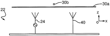
- FIG. 1 schematically shows, according to an xOz plane, an antenna system 22 according to a first embodiment of the invention.
- the antenna system 22 comprises an antenna 24 that is electrically short in the vertical plane, i.e. of which the height h is less than a quarter of the operating wavelength ⁇ 0 of the antenna 24 .
- the height h of the antenna 24 is between ⁇ 0 /200 and ⁇ 0 /5.
- the antenna 24 can be for example a whip antenna, or an antenna such as that described in FR2965978, filed by the applicant, and hereinafter referred to as the DAR antenna.
- the antenna is supplied with power by a generator 26 , and thus emits low-frequency, medium-frequency or high-frequency radiation, i.e. at an operating frequency of between 30 kHz and 30 MHz, and having vertical or elliptical polarization.
- the antenna 24 is connected to a conductive medium 28 having a surface that is substantially horizontal, i.e. substantially parallel to the xOy plane of the Oxyz orthogonal axis system.
- the conductive medium 28 is an imperfect conductive medium, for example earth (soil, sand, etc.) or water (sea, salt marsh, lake, etc.).
- the antenna system 22 further comprises a wired parasitic element 30 extending in a direction that is substantially parallel to the surface of the conductive medium 28 , in this case parallel to the Ox axis, and to a height H above the conductive medium 28 .
- the height H is generally between ⁇ 0 /200 and ⁇ 0 /2. However, the smaller the height H, the more the antenna system 22 will be unobtrusive and integrated into the landscape in which it is located.
- the wired parasitic element 30 is linear in this case, and is for example a (single-strand or multi-strand) wire or a conductive tube having a cylindrical or square cross section.
- the parasitic element 30 is supported by at least one insulating vertical post (not shown), preferably a plurality of insulating vertical posts (not shown) which are evenly distributed along the parasitic element 30 and fastened into the conductive medium 28 if the composition and depth thereof allows it, or said posts float on the conductive medium 28 if said medium consists of water.
- the parasitic element 30 is electrically insulated from the antenna and is arranged in the vicinity of the antenna 24 so as to be able to radiate by virtue of the current induced by the radiation from the antenna 24 .
- the parasitic element 30 is of a length L and is dimensioned such that the radiation from the antenna 24 and the radiation from the parasitic element 30 are in antiphase, and are of virtually the same amplitude in order to significantly reduce the radiation in the desired direction.
- the parasitic element 30 is centered on the antenna 24 , the antenna 24 thus being positioned in the region of the medium of the parasitic element 30 .
- the parasitic element 30 can be arranged in any desired manner in the vicinity of the antenna 24 from the moment that said parasitic element can radiate by virtue of the current induced by the radiation from the antenna 24 .
- the length L of the parasitic element 30 is therefore adapted depending on its placement relative to the antenna 24 , and generally varies between 0.9 ⁇ 0 and several ⁇ 0 .
- the obtained antenna system 22 is capable of emitting radiation in low-frequency, medium-frequency and high-frequency waves.
- the discontinuity between the air and the imperfect conductive medium 28 favors propagation of an omnidirectional or directional ground wave, known as a surface wave.
- the antenna 24 of the antenna system 22 can originally be an antenna which is intended to transmit surface waves, as with for example the DAR antenna, in which case the addition of the parasitic element 30 in order to form the antenna system 22 results in improved performance of the antenna.
- the antenna 24 of the system can also not be originally intended to transmit surface waves, in which case the addition of the parasitic element 30 makes it possible to use, for transmitting surface waves, an antenna which was not originally capable of this function.
- the antenna system can also operate as a signal receiver.
- This first embodiment is the simplest of the embodiments of the invention.
- the embodiments disclosed in the following are improvements on this first embodiment, and the features which have already been described for one embodiment will not be described again for an embodiment comprising these same features.
- FIG. 2 shows a radiation pattern according to an xOz plane of the antenna system according to the first embodiment of the invention.
- the pattern comprises three curves; a first curve 32 shows the radiation from a conventional DAR antenna, a second curve 34 shows an outline defining an ionospheric radiation area in which the antenna system should not radiate, and a third curve 36 showing the radiation from the antenna system according to the first embodiment of the invention.
- the area defined by the outline indicates that between ⁇ 45° and 45°, the radiation from the antenna system must not go beyond ⁇ 10 dB. It can be seen that the DAR antenna radiates in the area defined by the outline and thus does not comply with the limiting constraints of the ionospheric radiation.
- the antenna system in particular on account of the addition of parasitic elements, makes it possible to obtain radiation of surface waves that are close to the horizontal plane xOy shown by the axis ( ⁇ 90°; 90°) in the pattern. Furthermore, the ionospheric radiation from the antenna is reduced, and no radiation goes beyond ⁇ 10 dB in an angle of between ⁇ 45° and 45°, thus respecting the constraints of the outline. This radiation, the amplitude of which is less than 10 dB relative to the maximum radiation, is known as null radiation.
- FIG. 3 schematically shows, according to an xOz plane, an antenna system 22 according to a second embodiment of the invention.
- the conductive medium 28 has electrical conductivity that varies depending on its composition. For example, the sea, salt marshes or salt lakes have high electrical conductivity, and soil and sand have low electrical conductivity. If the electrical conductivity is too low, i.e. less than 1 S/m, the antenna system 22 is supplemented, as in the second embodiment, by a ground plane 38 , which is connected to the antenna 24 and is embedded below or on the surface of the conductive medium 28 .
- the ground plane 38 can be made up of a plate, or of a set of conductive wires forming a mesh, etc.
- the ground plane 38 can have various shapes, for example a circle, a polygon (regular or irregular polygon), etc.
- the ground plane 38 extends beneath the entirety of the antenna system 22 , that is to say the projection of the antenna system 22 onto the conductive medium 28 along the Oz axis is within the surface occupied by the ground plane 38 .
- the ground plane 38 has a minimum length that is strictly greater than the length L of the parasitic element 30 , and a minimum width that is at least several dozen centimeters greater than the width of the parasitic element 30 .
- the heights h and H defined above remain expressed starting from the conductive medium 28 .
- FIG. 4 schematically shows, according to a yOz plane, an antenna system 22 according to a third embodiment of the invention.
- FIG. 5 is a schematic perspective view of said antenna system 22 according to the third embodiment of the invention.
- the antenna system 22 comprises a first wired parasitic element 30 a , of a length L 1 , that is identical to the wired parasitic element from the first embodiment, as well as a second wired parasitic element 30 b , of a length L 2 , that is orthogonal to the first wired parasitic element 30 a and is positioned thereabove.
- the second wired parasitic element 30 b makes it possible to reduce the ionospheric radiation from the antenna 24 in a different plane from that of the first parasitic element 30 a .
- the second wired parasitic element 30 b is parallel to the Oy axis and thus reduces the ionospheric radiation in the xOz plane.
- the parasitic elements 30 a , 30 b are of lengths L 1 and L 2 which are preferably identical, but they can be of different lengths L 1 and L 2 in other embodiments.
- the heights H 1 and H 2 of the parasites 30 a , 30 b can be different or identical (in which case the parasitic elements 30 a , 30 b are electrically connected).
- the two parasitic elements 30 a , 30 b are centered on the antenna.
- the second parasitic element 30 b also makes it possible to improve the gain in the region of the ground above the conductive medium 28 and to obtain omnidirectionality of the radiation in the XoY plane, referred to as the azimuthal plane.
- the two parasitic elements can form any angle that is not 90°, or they can be off-center from the antenna. According to other embodiments of the invention, the two parasitic elements can be electrically connected. According to other embodiments, the antenna system can comprise more than two parasitic elements.
- FIG. 6 schematically shows, according to an xOz plane, an antenna system 22 according to a fourth embodiment of the invention.
- the antenna system 22 comprises two antennas that are connected to the conductive medium 28 , a first antenna 24 a of a height h 1 and a second antenna 24 b of a height h 2 , which are separated by distance d.
- the antenna system also comprises a single parasitic element 30 , arranged so as to radiate by virtue of the radiation from the two antennas 24 a , 24 b.
- the antenna system 22 makes it possible to modify the radiation from the antennas 24 a , 24 b by virtue of the parasitic element 30 and of the network theory applied to the two antennas 24 a , 24 b.
- FIG. 7 schematically shows, according to an xOz plane, an antenna system 22 according to a fifth embodiment of the invention.
- the antenna system 22 comprises a parasitic element 30 , an antenna 24 and a vertical parasitic element 40 , of a height h′ and arranged at distance d′ from the antenna 24 so as to radiate by virtue of the current induced by said radiation from the antenna 24 .
- the parasitic element 40 is connected to the conductive medium 28 , or to the ground plane in the embodiments where a ground plane is provided.
- the vertical parasitic element 40 radiates on account of its position in the vicinity of the antenna 24 , by electromagnetic coupling, and makes it possible to increase the directivity and/or the bandwidth of the antenna system 22 .
- the vertical parasitic element 40 can also have a shape that is similar to the antenna 24 without, however, being supplied with power.
- FIG. 8 schematically shows a radiation pattern according to the xOz plane of an antenna system according to this fifth embodiment.
- the pattern comprises three curves; a first curve 42 shows the radiation from a conventional DAR antenna, a second curve 44 shows an outline defining a radiation area in which the antenna system should not radiate, and a third curve 46 showing the radiation from the antenna system according to the fifth embodiment of the invention.
- the outline indicates that the amplitude of the radiated field must not go beyond ⁇ 10 dB between the angles 0° and 90° (on the vertical parasitic element side) and ⁇ 8 dB between ⁇ 45° and 0°.
- the antenna system according to the fifth embodiment makes it possible to respect this outline.
- FIG. 9 schematically shows, according to an xOz plane, an antenna system according to a sixth embodiment of the invention.
- This sixth embodiment is a combination of the third and fourth embodiments, the antenna system 22 comprising two parasitic elements 30 a , 30 b and two antennas 24 a , 24 b.
- FIG. 10 schematically shows, according to an xOz plane, an antenna system according to a seventh embodiment of the invention.
- This seventh embodiment is a combination of the third and fifth embodiments, the antenna system 22 comprising two parasitic elements 30 a , 30 b , an antenna 24 and a vertical parasitic element 40 .
- FIG. 11 schematically shows, according to an xOz plane, an antenna system according to an eighth embodiment of the invention.
- the antenna system 22 comprises an antenna 24 and a parasitic element 30 , the parasitic element 30 being electrically connected to the continuous medium 28 by vertical connectors, in this case two vertical connectors 48 a and 48 b , that are arranged symmetrically on either side of the antenna.
- the connectors 48 a , 48 b are connected in the region of the parasitic element 30 in positions in which the current distribution is at a maximum across the parasitic element 30 .
- the connectors 48 a , 48 b are connected in positions corresponding to a distance of ⁇ 0 /4 and 3 ⁇ 0 /4 starting from one of the parasitic element ends.
- FIG. 12 schematically shows a perspective view of an antenna system 22 according to a ninth embodiment of the invention.
- the antenna system 22 is a network of a plurality of antenna systems according to the embodiments described above, for example according to the first embodiment.
- the antenna system 22 thus comprises n antennas 24 - 24 n that are connected to the conductive medium 28 and n parasitic elements 30 - 30 n , each parasitic element being arranged in the vicinity of one antenna.
- the antennas are at a distance d from one another.
- the amplitude of the antenna positioned between the two other antennas is equal to 0.6 times the amplitude of said other antennas.
- the radiation in the xOz plane which can be seen in FIG. 13 , is similar to the radiation described with reference to FIG. 2 .
- FIG. 15 brings together a set of FIGS. 15 a , 15 b , 15 c , 15 d , 15 e , 15 f , 15 g and 15 h , showing, according to the xOy plane, various embodiments of wired parasitic elements 30 which can be used in an antenna system according to the invention.
- These parasitic elements comprise, on each of the ends thereof, a folded portion which makes it possible in particular to reduce the dimensions of the parasitic element, in the main direction thereof, with respect to a rectilinear wired parasitic element, while at the same time maintaining an electrical length that is equivalent to this rectilinear wired parasitic element.
- the electrical length of a parasitic element is the length of the longest current path on the parasitic element.
- the parasitic elements can comprise folded portions having different forms, such as meanders, windings, and various geometric shapes.
- the resulting dimensions can reach 65% of the dimensions of an equivalent rectilinear parasitic element, while at the same time maintaining an equivalent electrical length.
- FIG. 16 brings together a set of FIGS. 16 a , 16 b , 16 c and 16 d showing, according to an xOy plane, various embodiments of a plurality of wired parasitic elements forming a parasitic element known as a surface parasitic element 50 .
- the surface parasitic elements make it possible to increase the bandwidth of the antenna.
- a plurality of wired parasitic elements can be connected to form a parasitic element known as a volumetric parasitic element 52 in order to increase the bandwidth of the antenna.
- the shapes of the surface or volumetric parasitic elements can vary so as to reduce the width/length ratio of these parasitic elements in order to further increase the bandwidth.
- FIG. 18 brings together FIGS. 18 a and 18 b , showing, according to an xOy plane, two embodiments of the wired parasitic element 30 or the surface parasitic element 50 comprising at least one localized element, in this case two localized elements 54 a and 54 b , which can be resistive, capacitive (capacitor) or inductive (coil). These localized elements are widely referred to as a “load”.
- the localized elements 54 a , 54 b can make it possible to reproduce the RLC resonance of the parasitic element 30 so as to have a reduced physical length (or reduced dimensions) of the parasitic element 30 , but an equivalent electrical length.
- the localized elements 54 a , 54 b also make it possible to establish open (or high impedance) circuits having specific operating frequencies and closed circuits having other operating frequencies on the parasitic elements 30 , 50 , thus making it possible to vary the resonance of the parasitic elements according to the operating frequency.
- These localized elements 54 a , 54 b thus generate multiple resonances by means of current traps.
- the localized elements can also be used on the vertical parasitic elements and/or on the connectors of the parasitic elements.
- FIG. 19 brings together FIGS. 19 a , 19 b , 19 c and 19 d , showing perspective views of different embodiments of an antenna system 22 comprising an antenna 24 of the DAR kind, which antenna is connected to the conductive medium 28 (or to a ground plane if provided).
- the DAR antenna is made up of a loop extending in the xOz plane.
- a parasitic element 30 extends along the Oy axis, thus orthogonally to the DAR antenna, and in the vicinity of said DAR antenna.
- the various embodiments show various positions in which the parasitic element can be located.
- the parasitic element 30 is positioned above the DAR antenna.
- the parasitic element 30 is positioned below the maximum height of the DAR antenna, i.e. in the middle of the loop (without being connected thereto).
- the parasitic element 30 is offset by a distance d x from the DAR antenna along the Ox axis.
- the distance d x is at most equivalent to ⁇ 0 /2.
- the parasitic element 30 is offset by a distance d y from the DAR antenna along the Oy axis.
- the distance d y is at most equivalent to ⁇ 0 /2.
- the parasitic element can be offset in the xOy plane by combination of the distances d x and d y .
- FIG. 20 shows a radiation pattern according to the xOz plane of an antenna system according to the embodiment shown in FIG. 19 , for two wired parasitic element lengths.
- the ionospheric radiation (between ⁇ 45° and 45°) is low at this parasitic element length.
- the ionospheric radiation (angles between ⁇ 45° and 45°) is high at this parasitic element length, but the directivity is greater in the region of the surface waves (angles close to ⁇ 90° or 90°).
- Adjusting the length of the parasitic element between these two lengths thus make it possible to achieve intermediate results according to the application sought for the antenna system, favoring either the reduction of ionospheric radiation or the directivity in the region of the surface waves.
- the invention is not restricted only to the described embodiments.
- the features of the described embodiments can be combined to form other embodiments; the number and arrangement of the antennas, parasitic elements and parasitic elements can vary in order to obtain an antenna system which is the most suitable for the desired operation.
Abstract
Description
-
- at least one antenna which is electrically short in the vertical plane, has vertical or elliptical polarization and emits radiation, said antenna being connected to a conductive medium having a substantially horizontal surface,
-
- at least one wired parasitic element that is electrically insulated from each antenna and arranged in the vicinity of at least one antenna so as to be able to radiate by virtue of the current induced by said radiation from said antenna, said at least one wired parasitic element advantageously extending in a direction forming an angle of between −10° and 10° with the surface of the conductive medium.
Claims (9)
Applications Claiming Priority (3)
| Application Number | Priority Date | Filing Date | Title |
|---|---|---|---|
| FR1554426A FR3036543B1 (en) | 2015-05-18 | 2015-05-18 | SURFACE WAVE ANTENNA SYSTEM |
| FR1554426 | 2015-05-18 | ||
| PCT/FR2016/051151 WO2016185124A1 (en) | 2015-05-18 | 2016-05-13 | Surface wave antenna system |
Publications (2)
| Publication Number | Publication Date |
|---|---|
| US20180123218A1 US20180123218A1 (en) | 2018-05-03 |
| US10622697B2 true US10622697B2 (en) | 2020-04-14 |
Family
ID=54329616
Family Applications (1)
| Application Number | Title | Priority Date | Filing Date |
|---|---|---|---|
| US15/572,192 Active 2036-06-26 US10622697B2 (en) | 2015-05-18 | 2016-05-13 | Surface wave antenna system |
Country Status (8)
| Country | Link |
|---|---|
| US (1) | US10622697B2 (en) |
| EP (1) | EP3298651A1 (en) |
| CN (1) | CN107912072B (en) |
| AU (1) | AU2016263523B2 (en) |
| CA (1) | CA2985023C (en) |
| FR (1) | FR3036543B1 (en) |
| RU (1) | RU2709423C2 (en) |
| WO (1) | WO2016185124A1 (en) |
Families Citing this family (7)
| Publication number | Priority date | Publication date | Assignee | Title |
|---|---|---|---|---|
| US10408915B2 (en) | 2015-09-10 | 2019-09-10 | Cpg Technologies, Llc | Geolocation using guided surface waves |
| US10324163B2 (en) * | 2015-09-10 | 2019-06-18 | Cpg Technologies, Llc | Geolocation using guided surface waves |
| US10396566B2 (en) | 2015-09-10 | 2019-08-27 | Cpg Technologies, Llc | Geolocation using guided surface waves |
| US10193229B2 (en) * | 2015-09-10 | 2019-01-29 | Cpg Technologies, Llc | Magnetic coils having cores with high magnetic permeability |
| US10408916B2 (en) | 2015-09-10 | 2019-09-10 | Cpg Technologies, Llc | Geolocation using guided surface waves |
| FR3056831B1 (en) * | 2016-09-26 | 2019-08-02 | Tdf | ANTENNA WITH FERROMAGNETIC RODS FITTED AND COUPLED BETWEEN THEM |
| CN111600128A (en) * | 2020-05-27 | 2020-08-28 | 西安朗普达通信科技有限公司 | Novel decoupling surface coating |
Citations (25)
| Publication number | Priority date | Publication date | Assignee | Title |
|---|---|---|---|---|
| US2008931A (en) * | 1934-04-30 | 1935-07-23 | Int Stacey Corp | Antenna |
| US2212245A (en) | 1937-06-11 | 1940-08-20 | Int Standard Electric Corp | Antenna network for vehicle guiding systems |
| US3289208A (en) | 1962-02-12 | 1966-11-29 | Hollingsworth R Lee | Anti-sky wave radiating system |
| US4611214A (en) * | 1984-06-27 | 1986-09-09 | The United States Of America As Represented By The Secretary Of The Army | Tactical high frequency array antennas |
| US4658266A (en) * | 1983-10-13 | 1987-04-14 | Doty Archibald C Jun | Vertical antenna with improved artificial ground system |
| JPH0270104A (en) | 1988-06-14 | 1990-03-09 | Koden Electron Co Ltd | Wide directional microstrip antenna |
| US5173715A (en) * | 1989-12-04 | 1992-12-22 | Trimble Navigation | Antenna with curved dipole elements |
| US5629713A (en) | 1995-05-17 | 1997-05-13 | Allen Telecom Group, Inc. | Horizontally polarized antenna array having extended E-plane beam width and method for accomplishing beam width extension |
| US5900842A (en) * | 1997-09-20 | 1999-05-04 | Lucent Technologies, Inc. | Inexpensive directional antenna that is easily tuned and weather resistant |
| US6476766B1 (en) * | 1997-11-07 | 2002-11-05 | Nathan Cohen | Fractal antenna ground counterpoise, ground planes, and loading elements and microstrip patch antennas with fractal structure |
| US6693600B1 (en) * | 2000-11-24 | 2004-02-17 | Paul G. Elliot | Ultra-broadband antenna achieved by combining a monocone with other antennas |
| US20040140944A1 (en) * | 2003-01-22 | 2004-07-22 | Pennington Billy D. | Inverted ground plane system |
| US20050174297A1 (en) * | 2004-02-09 | 2005-08-11 | Cake Brian V. | Compact ground-plane antenna |
| US20050195124A1 (en) * | 2002-09-10 | 2005-09-08 | Carles Puente Baliarda | Coupled multiband antennas |
| US20050237258A1 (en) * | 2002-03-27 | 2005-10-27 | Abramov Oleg Y | Switched multi-beam antenna |
| US20060103584A1 (en) * | 2004-11-18 | 2006-05-18 | Hon Hai Precision Ind. Co., Ltd. | Impedance matching means between antenna and transmission line |
| US20080030406A1 (en) * | 2006-05-30 | 2008-02-07 | Solidica, Inc. | Omni-directional antenna |
| US20080266190A1 (en) * | 2007-04-27 | 2008-10-30 | Kabushiki Kaisha Toshiba | Tunable antenna device and radio apparatus |
| US20120086603A1 (en) | 2010-10-07 | 2012-04-12 | Electronics And Telecommunications Research Institute | Method and apparatus for adjusting horizontal beam of omni-directions antenna |
| US20120146872A1 (en) | 2009-06-11 | 2012-06-14 | Sebastien Chainon | Antenna radiating element |
| US20130241790A1 (en) * | 2010-10-07 | 2013-09-19 | Tdf | Large-area broadband surface-wave antenna |
| US20160197669A1 (en) * | 2014-12-11 | 2016-07-07 | Tesla Wireless Company LLC | Communication method and system that uses low latency/low data bandwidth and high latency/high data bandwidth pathways |
| US20170047665A1 (en) * | 2015-08-12 | 2017-02-16 | Novatel, Inc. | Patch antenna with peripheral parasitic monopole circular arrays |
| US9941588B2 (en) * | 2007-08-20 | 2018-04-10 | Ethertronics, Inc. | Antenna with multiple coupled regions |
| US20190165477A1 (en) * | 2015-08-10 | 2019-05-30 | Tdf | Surface-wave antenna, antenna array and use of an antenna or an antenna array |
Family Cites Families (5)
| Publication number | Priority date | Publication date | Assignee | Title |
|---|---|---|---|---|
| JP4053144B2 (en) * | 1998-07-10 | 2008-02-27 | 日本電業工作株式会社 | Dual-polarized antenna |
| US6211824B1 (en) * | 1999-05-06 | 2001-04-03 | Raytheon Company | Microstrip patch antenna |
| WO2004027921A2 (en) * | 2002-09-17 | 2004-04-01 | Ipr Licensing, Inc. | Multiple pattern antenna |
| CN201985254U (en) * | 2011-03-25 | 2011-09-21 | 星动通讯科技(苏州)有限公司 | Double frequency band array antenna |
| KR20140004954A (en) * | 2012-07-03 | 2014-01-14 | 콘티넨탈 오토모티브 시스템 주식회사 | Method for diagnosing error of can communication |
-
2015
- 2015-05-18 FR FR1554426A patent/FR3036543B1/en active Active
-
2016
- 2016-05-13 EP EP16726367.2A patent/EP3298651A1/en active Pending
- 2016-05-13 CN CN201680027953.4A patent/CN107912072B/en active Active
- 2016-05-13 CA CA2985023A patent/CA2985023C/en active Active
- 2016-05-13 US US15/572,192 patent/US10622697B2/en active Active
- 2016-05-13 AU AU2016263523A patent/AU2016263523B2/en active Active
- 2016-05-13 RU RU2017138384A patent/RU2709423C2/en active
- 2016-05-13 WO PCT/FR2016/051151 patent/WO2016185124A1/en active Application Filing
Patent Citations (27)
| Publication number | Priority date | Publication date | Assignee | Title |
|---|---|---|---|---|
| US2008931A (en) * | 1934-04-30 | 1935-07-23 | Int Stacey Corp | Antenna |
| US2212245A (en) | 1937-06-11 | 1940-08-20 | Int Standard Electric Corp | Antenna network for vehicle guiding systems |
| US3289208A (en) | 1962-02-12 | 1966-11-29 | Hollingsworth R Lee | Anti-sky wave radiating system |
| US4658266A (en) * | 1983-10-13 | 1987-04-14 | Doty Archibald C Jun | Vertical antenna with improved artificial ground system |
| US4611214A (en) * | 1984-06-27 | 1986-09-09 | The United States Of America As Represented By The Secretary Of The Army | Tactical high frequency array antennas |
| JPH0270104A (en) | 1988-06-14 | 1990-03-09 | Koden Electron Co Ltd | Wide directional microstrip antenna |
| US5173715A (en) * | 1989-12-04 | 1992-12-22 | Trimble Navigation | Antenna with curved dipole elements |
| US5629713A (en) | 1995-05-17 | 1997-05-13 | Allen Telecom Group, Inc. | Horizontally polarized antenna array having extended E-plane beam width and method for accomplishing beam width extension |
| US5900842A (en) * | 1997-09-20 | 1999-05-04 | Lucent Technologies, Inc. | Inexpensive directional antenna that is easily tuned and weather resistant |
| US6476766B1 (en) * | 1997-11-07 | 2002-11-05 | Nathan Cohen | Fractal antenna ground counterpoise, ground planes, and loading elements and microstrip patch antennas with fractal structure |
| US6693600B1 (en) * | 2000-11-24 | 2004-02-17 | Paul G. Elliot | Ultra-broadband antenna achieved by combining a monocone with other antennas |
| US20050237258A1 (en) * | 2002-03-27 | 2005-10-27 | Abramov Oleg Y | Switched multi-beam antenna |
| US7315289B2 (en) * | 2002-09-10 | 2008-01-01 | Fractus, S.A. | Coupled multiband antennas |
| US20050195124A1 (en) * | 2002-09-10 | 2005-09-08 | Carles Puente Baliarda | Coupled multiband antennas |
| US20040140944A1 (en) * | 2003-01-22 | 2004-07-22 | Pennington Billy D. | Inverted ground plane system |
| US20050174297A1 (en) * | 2004-02-09 | 2005-08-11 | Cake Brian V. | Compact ground-plane antenna |
| US20060103584A1 (en) * | 2004-11-18 | 2006-05-18 | Hon Hai Precision Ind. Co., Ltd. | Impedance matching means between antenna and transmission line |
| US7339545B2 (en) * | 2004-11-18 | 2008-03-04 | Hon Hai Precision Ind. Co., Ltd. | Impedance matching means between antenna and transmission line |
| US20080030406A1 (en) * | 2006-05-30 | 2008-02-07 | Solidica, Inc. | Omni-directional antenna |
| US20080266190A1 (en) * | 2007-04-27 | 2008-10-30 | Kabushiki Kaisha Toshiba | Tunable antenna device and radio apparatus |
| US9941588B2 (en) * | 2007-08-20 | 2018-04-10 | Ethertronics, Inc. | Antenna with multiple coupled regions |
| US20120146872A1 (en) | 2009-06-11 | 2012-06-14 | Sebastien Chainon | Antenna radiating element |
| US20120086603A1 (en) | 2010-10-07 | 2012-04-12 | Electronics And Telecommunications Research Institute | Method and apparatus for adjusting horizontal beam of omni-directions antenna |
| US20130241790A1 (en) * | 2010-10-07 | 2013-09-19 | Tdf | Large-area broadband surface-wave antenna |
| US20160197669A1 (en) * | 2014-12-11 | 2016-07-07 | Tesla Wireless Company LLC | Communication method and system that uses low latency/low data bandwidth and high latency/high data bandwidth pathways |
| US20190165477A1 (en) * | 2015-08-10 | 2019-05-30 | Tdf | Surface-wave antenna, antenna array and use of an antenna or an antenna array |
| US20170047665A1 (en) * | 2015-08-12 | 2017-02-16 | Novatel, Inc. | Patch antenna with peripheral parasitic monopole circular arrays |
Non-Patent Citations (2)
| Title |
|---|
| Fikioris G et al: "Novel surface-wave antenna", IEE Proceedings: Microwaves, Antennas and Propagation, IEE, Stevenage, Herts, GB, vol. 143, No. 1, Feb. 16, 1996 (Feb. 16, 1996), pp. 1-6, XP006006537, ISSN: 1350-2417, DOI: 10.1049/IP-MAP:19960160. |
| FIKIORIS G., KING R.W.P., WU T.T.: "Novel surface-wave antenna", IEE PROCEEDINGS: MICROWAVES, ANTENNAS AND PROPAGATION., IEE, STEVENAGE, HERTS., GB, vol. 143, no. 1, 16 February 1996 (1996-02-16), GB, pages 1 - 6, XP006006537, ISSN: 1350-2417, DOI: 10.1049/ip-map:19960160 |
Also Published As
| Publication number | Publication date |
|---|---|
| WO2016185124A1 (en) | 2016-11-24 |
| RU2709423C2 (en) | 2019-12-17 |
| AU2016263523A1 (en) | 2017-11-30 |
| CN107912072A (en) | 2018-04-13 |
| CA2985023A1 (en) | 2016-11-24 |
| US20180123218A1 (en) | 2018-05-03 |
| EP3298651A1 (en) | 2018-03-28 |
| FR3036543A1 (en) | 2016-11-25 |
| FR3036543B1 (en) | 2017-05-12 |
| CN107912072B (en) | 2021-03-02 |
| RU2017138384A (en) | 2019-06-18 |
| RU2017138384A3 (en) | 2019-06-18 |
| AU2016263523B2 (en) | 2019-11-21 |
| CA2985023C (en) | 2023-12-12 |
Similar Documents
| Publication | Publication Date | Title |
|---|---|---|
| US10622697B2 (en) | Surface wave antenna system | |
| US11431087B2 (en) | Wideband, low profile, small area, circular polarized UHF antenna | |
| CN107615588B (en) | Patch antenna system | |
| US5629713A (en) | Horizontally polarized antenna array having extended E-plane beam width and method for accomplishing beam width extension | |
| US20170201024A1 (en) | Radar array antenna | |
| US20140266953A1 (en) | Antenna having split directors and antenna array comprising same | |
| JP3734666B2 (en) | ANTENNA DEVICE AND ARRAY ANTENNA USING THE SAME | |
| CN109075436A (en) | Ultra wideband dual polarization radiating element for antenna for base station | |
| US8643556B2 (en) | Receiving aerial for circularly polarized radio signals | |
| US20130241790A1 (en) | Large-area broadband surface-wave antenna | |
| US9799956B2 (en) | Three-dimensional compound loop antenna | |
| KR101111578B1 (en) | Dual polarized antenna for bidirectional communication | |
| CN110419144A (en) | Antenna element and aerial array | |
| CN105144483B (en) | Circular polarized antenna | |
| AU2016307384B2 (en) | Surface-wave antenna, antenna array and use of an antenna or an antenna array | |
| US7791555B2 (en) | High gain multiple polarization antenna assembly | |
| KR101288237B1 (en) | Patch Antenna for Receiving Circular Polarization and Linear Polarization | |
| CN103794853B (en) | Omnidirectional antenna | |
| KR101104371B1 (en) | Omni antenna | |
| WO2020133224A1 (en) | Antenna unit and array antenna | |
| Takano et al. | A partially driven array antenna backed by a reflector with a reduction in the number of driven elements by up to 67% | |
| KR102020489B1 (en) | Antenna Apparatus | |
| GB2480435A (en) | Directional antenna with a leaky wave structure and a high impedance surface arrangement | |
| Rohani et al. | Analysis of super directive array with switchable beam pattern | |
| JP5983089B2 (en) | Antenna and radio communication apparatus provided with the same |
Legal Events
| Date | Code | Title | Description |
|---|---|---|---|
| FEPP | Fee payment procedure |
Free format text: ENTITY STATUS SET TO UNDISCOUNTED (ORIGINAL EVENT CODE: BIG.); ENTITY STATUS OF PATENT OWNER: LARGE ENTITY |
|
| AS | Assignment |
Owner name: UNIVERSITE DE RENNES 1, FRANCE Free format text: ASSIGNMENT OF ASSIGNORS INTEREST;ASSIGNORS:COLOMBEL, FRANCK;AVRILLON, STEPHANE;REEL/FRAME:045558/0898 Effective date: 20171219 Owner name: TDF, FRANCE Free format text: ASSIGNMENT OF ASSIGNORS INTEREST;ASSIGNORS:BELLEC, MATHILDE;PALUD, SEBASTIEN;JEZEQUEL, PIERRE-YVES;SIGNING DATES FROM 20171115 TO 20171127;REEL/FRAME:045558/0782 |
|
| STPP | Information on status: patent application and granting procedure in general |
Free format text: NON FINAL ACTION MAILED |
|
| STPP | Information on status: patent application and granting procedure in general |
Free format text: RESPONSE TO NON-FINAL OFFICE ACTION ENTERED AND FORWARDED TO EXAMINER |
|
| STPP | Information on status: patent application and granting procedure in general |
Free format text: FINAL REJECTION MAILED |
|
| STPP | Information on status: patent application and granting procedure in general |
Free format text: DOCKETED NEW CASE - READY FOR EXAMINATION |
|
| STPP | Information on status: patent application and granting procedure in general |
Free format text: NOTICE OF ALLOWANCE MAILED -- APPLICATION RECEIVED IN OFFICE OF PUBLICATIONS |
|
| STPP | Information on status: patent application and granting procedure in general |
Free format text: AWAITING TC RESP., ISSUE FEE NOT PAID |
|
| STCF | Information on status: patent grant |
Free format text: PATENTED CASE |
|
| MAFP | Maintenance fee payment |
Free format text: PAYMENT OF MAINTENANCE FEE, 4TH YEAR, LARGE ENTITY (ORIGINAL EVENT CODE: M1551); ENTITY STATUS OF PATENT OWNER: LARGE ENTITY Year of fee payment: 4 |
|
| AS | Assignment |
Owner name: UNIVERSITE DE RENNES, FRANCE Free format text: MERGER;ASSIGNOR:UNIVERSITE DE RENNES I;REEL/FRAME:065490/0667 Effective date: 20220324 |