US10620541B2 - Mask plate, exposure system and exposure method - Google Patents
Mask plate, exposure system and exposure method Download PDFInfo
- Publication number
- US10620541B2 US10620541B2 US15/503,926 US201615503926A US10620541B2 US 10620541 B2 US10620541 B2 US 10620541B2 US 201615503926 A US201615503926 A US 201615503926A US 10620541 B2 US10620541 B2 US 10620541B2
- Authority
- US
- United States
- Prior art keywords
- mask
- light
- control
- sub
- mask plate
- Prior art date
- Legal status (The legal status is an assumption and is not a legal conclusion. Google has not performed a legal analysis and makes no representation as to the accuracy of the status listed.)
- Active, expires
Links
- 238000000034 method Methods 0.000 title claims abstract description 31
- 239000004973 liquid crystal related substance Substances 0.000 claims abstract description 71
- 210000002858 crystal cell Anatomy 0.000 claims abstract description 32
- 239000003795 chemical substances by application Substances 0.000 claims description 36
- 239000000758 substrate Substances 0.000 claims description 32
- 239000004983 Polymer Dispersed Liquid Crystal Substances 0.000 claims description 12
- 239000010409 thin film Substances 0.000 claims description 6
- 238000005192 partition Methods 0.000 claims description 2
- 238000004519 manufacturing process Methods 0.000 abstract description 13
- 238000011112 process operation Methods 0.000 abstract 1
- 238000010586 diagram Methods 0.000 description 6
- 238000000059 patterning Methods 0.000 description 5
- 102100036464 Activated RNA polymerase II transcriptional coactivator p15 Human genes 0.000 description 4
- 101000713904 Homo sapiens Activated RNA polymerase II transcriptional coactivator p15 Proteins 0.000 description 4
- 229910004444 SUB1 Inorganic materials 0.000 description 4
- 229910004438 SUB2 Inorganic materials 0.000 description 4
- 101100311330 Schizosaccharomyces pombe (strain 972 / ATCC 24843) uap56 gene Proteins 0.000 description 4
- 238000005265 energy consumption Methods 0.000 description 4
- 101150018444 sub2 gene Proteins 0.000 description 4
- 230000005684 electric field Effects 0.000 description 3
- 239000010408 film Substances 0.000 description 2
- 230000003287 optical effect Effects 0.000 description 2
- 239000002245 particle Substances 0.000 description 2
- 238000009281 ultraviolet germicidal irradiation Methods 0.000 description 2
- 230000005540 biological transmission Effects 0.000 description 1
- 230000015572 biosynthetic process Effects 0.000 description 1
- 210000004027 cell Anatomy 0.000 description 1
- 239000004020 conductor Substances 0.000 description 1
- 238000005516 engineering process Methods 0.000 description 1
- 239000011521 glass Substances 0.000 description 1
- 238000010438 heat treatment Methods 0.000 description 1
- 238000006116 polymerization reaction Methods 0.000 description 1
- 238000009877 rendering Methods 0.000 description 1
- 230000010076 replication Effects 0.000 description 1
- 239000000565 sealant Substances 0.000 description 1
Images


Classifications
-
- G—PHYSICS
- G03—PHOTOGRAPHY; CINEMATOGRAPHY; ANALOGOUS TECHNIQUES USING WAVES OTHER THAN OPTICAL WAVES; ELECTROGRAPHY; HOLOGRAPHY
- G03F—PHOTOMECHANICAL PRODUCTION OF TEXTURED OR PATTERNED SURFACES, e.g. FOR PRINTING, FOR PROCESSING OF SEMICONDUCTOR DEVICES; MATERIALS THEREFOR; ORIGINALS THEREFOR; APPARATUS SPECIALLY ADAPTED THEREFOR
- G03F7/00—Photomechanical, e.g. photolithographic, production of textured or patterned surfaces, e.g. printing surfaces; Materials therefor, e.g. comprising photoresists; Apparatus specially adapted therefor
- G03F7/20—Exposure; Apparatus therefor
- G03F7/2051—Exposure without an original mask, e.g. using a programmed deflection of a point source, by scanning, by drawing with a light beam, using an addressed light or corpuscular source
- G03F7/2057—Exposure without an original mask, e.g. using a programmed deflection of a point source, by scanning, by drawing with a light beam, using an addressed light or corpuscular source using an addressed light valve, e.g. a liquid crystal device
-
- G—PHYSICS
- G02—OPTICS
- G02F—OPTICAL DEVICES OR ARRANGEMENTS FOR THE CONTROL OF LIGHT BY MODIFICATION OF THE OPTICAL PROPERTIES OF THE MEDIA OF THE ELEMENTS INVOLVED THEREIN; NON-LINEAR OPTICS; FREQUENCY-CHANGING OF LIGHT; OPTICAL LOGIC ELEMENTS; OPTICAL ANALOGUE/DIGITAL CONVERTERS
- G02F1/00—Devices or arrangements for the control of the intensity, colour, phase, polarisation or direction of light arriving from an independent light source, e.g. switching, gating or modulating; Non-linear optics
- G02F1/01—Devices or arrangements for the control of the intensity, colour, phase, polarisation or direction of light arriving from an independent light source, e.g. switching, gating or modulating; Non-linear optics for the control of the intensity, phase, polarisation or colour
- G02F1/13—Devices or arrangements for the control of the intensity, colour, phase, polarisation or direction of light arriving from an independent light source, e.g. switching, gating or modulating; Non-linear optics for the control of the intensity, phase, polarisation or colour based on liquid crystals, e.g. single liquid crystal display cells
- G02F1/133—Constructional arrangements; Operation of liquid crystal cells; Circuit arrangements
- G02F1/1333—Constructional arrangements; Manufacturing methods
- G02F1/1339—Gaskets; Spacers; Sealing of cells
-
- G—PHYSICS
- G02—OPTICS
- G02F—OPTICAL DEVICES OR ARRANGEMENTS FOR THE CONTROL OF LIGHT BY MODIFICATION OF THE OPTICAL PROPERTIES OF THE MEDIA OF THE ELEMENTS INVOLVED THEREIN; NON-LINEAR OPTICS; FREQUENCY-CHANGING OF LIGHT; OPTICAL LOGIC ELEMENTS; OPTICAL ANALOGUE/DIGITAL CONVERTERS
- G02F1/00—Devices or arrangements for the control of the intensity, colour, phase, polarisation or direction of light arriving from an independent light source, e.g. switching, gating or modulating; Non-linear optics
- G02F1/01—Devices or arrangements for the control of the intensity, colour, phase, polarisation or direction of light arriving from an independent light source, e.g. switching, gating or modulating; Non-linear optics for the control of the intensity, phase, polarisation or colour
- G02F1/13—Devices or arrangements for the control of the intensity, colour, phase, polarisation or direction of light arriving from an independent light source, e.g. switching, gating or modulating; Non-linear optics for the control of the intensity, phase, polarisation or colour based on liquid crystals, e.g. single liquid crystal display cells
- G02F1/133—Constructional arrangements; Operation of liquid crystal cells; Circuit arrangements
- G02F1/13306—Circuit arrangements or driving methods for the control of single liquid crystal cells
-
- G—PHYSICS
- G02—OPTICS
- G02F—OPTICAL DEVICES OR ARRANGEMENTS FOR THE CONTROL OF LIGHT BY MODIFICATION OF THE OPTICAL PROPERTIES OF THE MEDIA OF THE ELEMENTS INVOLVED THEREIN; NON-LINEAR OPTICS; FREQUENCY-CHANGING OF LIGHT; OPTICAL LOGIC ELEMENTS; OPTICAL ANALOGUE/DIGITAL CONVERTERS
- G02F1/00—Devices or arrangements for the control of the intensity, colour, phase, polarisation or direction of light arriving from an independent light source, e.g. switching, gating or modulating; Non-linear optics
- G02F1/01—Devices or arrangements for the control of the intensity, colour, phase, polarisation or direction of light arriving from an independent light source, e.g. switching, gating or modulating; Non-linear optics for the control of the intensity, phase, polarisation or colour
- G02F1/13—Devices or arrangements for the control of the intensity, colour, phase, polarisation or direction of light arriving from an independent light source, e.g. switching, gating or modulating; Non-linear optics for the control of the intensity, phase, polarisation or colour based on liquid crystals, e.g. single liquid crystal display cells
- G02F1/133—Constructional arrangements; Operation of liquid crystal cells; Circuit arrangements
- G02F1/1333—Constructional arrangements; Manufacturing methods
- G02F1/1334—Constructional arrangements; Manufacturing methods based on polymer dispersed liquid crystals, e.g. microencapsulated liquid crystals
Definitions
- Embodiments of the disclosure relate to the field of display technologies, more particularly, to a mask plate, an exposure system and an exposure method.
- a mask plate is used as a tool for transferring fine patterns in mass replication and production of mask fabrication processes, which plays an important role in the fabrication of substrates. Especially during the curing of sealant, it is achieved under the protection of the mask plate, otherwise faulty display will be generated.
- different products have different patterns, which means mask plates with different patterns have to be used. In real production, different mask plates also have to be changed frequently to manufacture different products.
- Mask plates are normally of a high price. Meanwhile, any fault caused during the design, manufacture, transmission, storage or replacement and mounting processes will make a mask plate unusable, which causes the designers, producers and users of the mask plates much trouble and economic losses.
- a mask plate which comprises a control unit and a liquid crystal cell, wherein the control unit is electrically connected to the liquid crystal cell and configured to control the liquid crystal cell to render a mask pattern.
- an exposure system which comprises the above-mentioned mask plate.
- an exposure method performed by using the above-mentioned mask plate comprises: determining a control signal according to a mask pattern; inputting the control signal to the control unit such that the control unit controls the liquid crystal cell to render the mask pattern; and exposing a substrate to be exposed by using the mask plate.
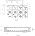
- FIG. 1 schematically illustrates a diagram of a mask plate in accordance with an embodiment of the disclosure
- FIG. 2 a schematically illustrates a diagram of a mask plate in accordance with another embodiment of the disclosure
- FIG. 2 b schematically illustrates a partial diagram of a mask plate in accordance with an embodiment of the disclosure
- FIG. 2 c schematically illustrates a cross section view of a liquid crystal cell in accordance with an embodiment of the disclosure
- FIG. 3 a schematically illustrates a pattern of a seal agent
- FIG. 3 b schematically illustrates a pattern of a mask plate according to the pattern of the seal agent of FIG. 3 a;
- FIG. 4 schematically illustrates a diagram of a fabrication process of a liquid crystal cell
- FIG. 5 schematically illustrates a flow chart of an exposure method in accordance with an embodiment of the disclosure.
- FIG. 1 schematically illustrates a diagram of a mask plate in accordance with an embodiment of the disclosure.
- the mask plate comprise a control unit 10 and a liquid crystal cell 20 , wherein the control unit 10 is electrically connected to the liquid crystal cell 20 and configured to control the liquid crystal cell 20 to render a predetermined mask pattern.
- the above mask plate renders various mask patterns as needed.
- the embodiment makes it possible for one mask plate to correspond to products needing various mask patterns, which not only avoids designing of various mask plates, but also saves mask cost as multiple mask plates are no longer needed.
- UV irradiation is performed without changing the mask plate during the production, the mask plate does not need to be dismounted during its life span, which is of a simple process and saves energy consumption.
- the embodiment provides a mask plate comprising a control unit and a liquid crystal cell.
- the mask plate further comprises a plurality of gate lines GL and a plurality of data lines DL, the plurality of gate lines GL and the plurality of data lines DL intersect each other to partition the liquid crystal cell into a plurality of mask sub-regions MS arranged as an array.
- the control unit comprises a plurality of control switches CS, each mask sub-region MS has a control switch CS disposed therein, and the control switch CS is configured to control light-transmitting state of the mask sub-region MS.
- the light-transmitting states comprise light-fully-transmitted state, light-tight state and grayscale-transmitted (i.e., light-partially-transmitted) state.
- a region consisting of at least two mask sub-regions MS is referred to as a mask block MB.
- the liquid crystal cell 20 comprises a plurality of mask sub-regions MS arranged as an array (m rows and n columns), each mask sub-region MS has a corresponding control switch CS, such as a Thin Film Transistor (TFT) disposed therein.
- the control unit 10 realizes the control of the individual regions of the liquid crystal cell 20 by controlling each TFT.
- a predetermined mask pattern typically comprises a fully-exposed region, a non-exposed region and a partially-exposed region.
- Liquid crystals in the mask sub-regions corresponding to the fully-exposed regions are in the light-fully-transmitting state.
- Liquid crystals in the mask sub-regions corresponding to the non-exposed regions are in the light-tight state.
- Liquid crystals in the mask sub-regions corresponding to the partially-exposed regions are in the light-partially-transmitted state.
- control unit 10 controls the control switches CS corresponding to respective mask sub-regions according to the control signals, such that the respective control switches CS control the light-transmitting states of liquid crystals in the corresponding mask sub-regions and allow the mask plate to eventually render the predetermined mask pattern.
- FIG. 2 c schematically illustrates a cross section view of a liquid crystal cell comprising a plurality of mask sub-regions.
- each mask sub-region MS comprises a first substrate SUB 1 and a second substrate SUB 2 disposed as opposed to each other; liquid crystals LC disposed between the first substrate SUB 1 and the second substrate SUB 2 ; a first electrode E 1 disposed between the first substrate SUB 1 and the liquid crystals LC; and a second electrode E 2 disposed between the second substrate SUB 2 and the liquid crystals LC.
- the first electrode E 1 is for example a common electrode
- the second electrode E 2 is for example a pixel electrode.
- the first substrate SUB 1 and the second substrate SUB 2 are made of transparent substrates, such as glass; the two electrodes are made of transparent electrically-conductive material such as ITO and the like.
- the plurality of mask sub-regions are connected to each other and at least one of the first electrode and the second electrode may be integral.
- the control switch is for example a TFT
- the TFT is configured to control the light-transmitting states of the corresponding mask sub-region, such as light-fully-transmitted state, light-tight state and light-partially-transmitted state.
- the TFT comprises a source electrode S, a drain electrode D and a gate electrode G, one of the source electrode S and the drain electrode D is connected to the data line DL, the other is connected to the second electrode E 2 , and the gate electrode G is connected to the gate line GL.
- the liquid crystals in the mask sub-regions are Polymer Dispersed Liquid Crystals (PDLCs).
- PDLCs Polymer Dispersed Liquid Crystals
- the PDLCs do not form a regular electric field, optical axes of the liquid crystal particles are randomly oriented and render a disorder state. Incident light is strongly scattered, and a non-transparent state is rendered.
- an external voltage for example an electric field E is applied between the first electrode E 1 and the second electrode E 2 in FIG. 2 c , the optical axes of the liquid crystal particles are aligned in a direction perpendicular to the film surface, which is in the same direction as the electric field, a transparent state is rendered.
- the control switches i.e., the TFTs, control the light-transmitting states of the PDLCs in the corresponding mask sub-regions according to the control signals, thereby allowing the liquid crystal cell to render the predetermined mask pattern.
- control unit 10 is configured to periodically scan or drive the TFT, such that the TFT controls the light-transmitting states of the liquid crystals in the corresponding mask sub-regions to remain the same during a predetermined time period.
- the liquid crystal cell 20 renders the mask pattern during the predetermined time period.
- a length of the predetermined time period may be adjusted as needed, such as from 5 minutes to 15 minutes.
- the on-off states of the TFTs in the corresponding mask sub-regions are controlled by the control signals, thereby controlling the light-transmitting states of the liquid crystals.
- the mask plate is used to cure seal agent
- the light-transmitting states of the respective mask sub-regions are controlled according to requirements of the pattern of the seal agent.
- FIG. 3 a which is a pattern of seal agent, where the white region is to be exposed, while the black regions need no exposure.
- control signals have to be designed first according to the pattern of seal agent as illustrated in FIG. 3 a , and then the control signals are input to the control unit, such that the control unit turns on/off the TFTs according to the control signals, which further controls the light-transmitting states of liquid crystals of the plurality of mask sub-regions.
- FIG. 3 b which is the mask pattern rendered by the mask plate under the control of the control signals.
- the light-transmitting state of the liquid crystals of the plurality of mask sub-regions corresponding to the exposed region of the seal agent pattern is light-fully-transmitted, and the light-transmitting state of the liquid crystals of the mask sub-regions corresponding to the non-exposed region of the seal agent pattern is light-tight.
- the mask pattern rendered by the above mask plate is relatively simple, as the embodiment is only for illustrative purpose. It can be contemplated that the mask plate may realize various simple or complicated mask patterns. This is because the mask plate described in the embodiment comprises a plurality of mask sub-region, and the light-transmitting states of the liquid crystals within the mask sub-regions arc controlled by the corresponding control switches. Therefore. the light-transmitting states of the liquid crystals within the mask sub-regions call be changed by changing the control signals, which in turn allows the mask plate to render the needed mask pattern.
- FIGS. 4 a to 4 e which schematically illustrates a diagram of a fabrication process of a liquid crystal cell of the above mask plate, an example of the liquid crystals LCs being PDLCs is described.
- steps of forming electrodes or dielectric layers in the liquid crystal cell are omitted.
- a person skilled in the art will understand that such formation steps may be performed as necessary.
- TFTs are fabricated on a substrate, and then PDLCs are dripped on the TFTs. After the dripping step, another substrate is cell-assembled therewith and packed. Finally, polymerization is performed by heating the cell, a PDLC film is formed on the TFT.
- it can control the light-transmitting states of the PDLCs by controlling power on-off state of the TFTs.
- the TFTs When the TFTs are powered off, the TFTs control the PDLCs in the corresponding regions to be in a light-tight state.
- the TFTs When the TFTs are powered on, the TFTs control the PDLCs in the corresponding regions to be in a light-fully-transmitted state.
- control unit is configured to control the on-off states of the TFTs in the corresponding mask sub-regions according to the control signals, thereby controlling the light-transmitting states of the liquid crystals, allowing the mask plate to render a predetermined mask pattern.
- the embodiment makes it possible for one mask plate to correspond to various mask patterns. In this way, it is no longer necessary to design multiple mask plates for various mask patterns, which saves the trouble of designing various mask plates. In the meantime, as multiple mask plates are no longer needed, the cost of mask plates is also reduced.
- UV irradiation may be performed without changing the mask plate. As a result, the mask plate does not need to be dismounted during its life span, which is of a simple process and saves energy consumption.
- the embodiment of the disclosure provides an exposure system, comprising the mask plate as described in any of the above embodiments.
- the mask pattern is a seal agent pattern.
- the liquid crystal cell is partitioned into a plurality of mask sub-regions arranged into an array, at least two mask sub-region forms a mask block;
- the control unit is configured to control light-transmitting states of the mask blocks such that the mask plate renders the seal agent pattern.
- the exposure system further comprises a light source device.
- the light source device is for example a UV light source device.
- the mask plate can render the seal agent pattern by being controlled through the mask blocks of the mask plate, instead of being controlled through respective mask sub-regions of the mask plate one by one, herein, each of mask blocks includes at least two mask sub-regions.
- the control unit controls the mask blocks according to the control signals such that the mask plate renders the seal agent pattern.
- the control signals are generated according to the predetermined seal agent pattern.
- the mask plate is placed on a substrate to be patterned (or exposed), and then the control signals are determined according to the exposed pattern, next, the control signals are input to the control unit, such that the control unit controls the liquid crystal cell to render the predetermined exposed pattern according to the control signals. Finally, UV light emitted by the UV light source device is used to irradiate the mask plate rendering the exposed pattern, thereby finishing the patterning process of the substrate.
- the mask plate of the above embodiments since the mask plate of the above embodiments is used, the mask plate can be controlled as needed to render various mask patterns. As a result, a single exposure system can correspond to products needing various mask patterns. When various mask patterns are needed, patterning processes thereof can be accomplished without changing the mask plate. As a result, the mask plate does not need to be dismounted during its life span, which is of a simple process and saves energy consumption. In the meantime, considering that mask plates are of relatively high cost, not requiring unmounting from time to time can also help to reduce wearing to the mask plates caused during the unmounting process, which makes the life span of the mask plates longer and cost lower. At the same time, as one mask plate can be used to render various mask patterns, it is no longer necessary to design multiple mask plates having different patterns, which also reduces the design and fabrication cost of the mask plates.
- the embodiment provides an exposing method (also referred as “patterning process”) performed by using the mask plate described in any of the embodiments.
- the method comprises the following steps:
- Step 101 determining a control signal according to a mask pattern.
- the mask pattern is for example a seal agent pattern.
- the control signal comprises information such as regions in the seal agent pattern which need to be fully-exposed, not exposed or partially-exposed.
- Step 102 inputting the control signal to a control unit such that the control unit controls the liquid crystal cell to render the mask pattern.
- the mask plate comprises for example a plurality of mask sub-regions arranged along directions of rows and columns, each mask sub-region has a corresponding control switch disposed therein.
- the control switch is configured to control light-transmitting states of the liquid crystals of the corresponding mask sub-region according to the control signals determined in step 101 , such that the liquid crystal cell renders the predetermined mask pattern.
- the control switch is for example a TFT.
- the light-transmitting state of liquid crystals of the corresponding mask sub-region controlled by the TFT according to the control signal may be light-fully-transmitted, light-tight and light-partially-transmitted.
- the control unit controls the light-transmitting state of the liquid crystals of the mask sub-regions corresponding to the fully-exposed region to be light-fully-transmitted, controls the light-transmitting state of the liquid crystals of the mask sub-regions corresponding to the non-exposed region to be light-tight, and controls the light-transmitting state of the liquid crystals of the mask sub-regions corresponding to the partially-exposed region to be light-partially-transmitted.
- Step 103 exposing a substrate to be exposed by using the above mask plate.
- the mask plate has already rendered the predetermined mask pattern in step 102 , in this step it only needs to use the mask plate to expose the substrate, thereby finishing the patterning process.
- the substrate is a substrate on which the seal agent is to be cured
- the predetermined exposed pattern is the seal agent pattern.
- the mask plate of the above embodiments when used to cure seal agent, because the seal agent pattern is relatively simple, the mask plate can render the seal agent pattern by being controlled through the mask blocks of the mask plate, instead of being controlled through respective mask sub-regions of the mask plate one by one, herein, each of mask blocks includes at least two mask sub-regions. Such an operation simplifies the control method.
- control signals are determined according to the seal agent pattern and then input to the control unit, such that the control unit controls the multiple mask blocks to render the predetermined exposing pattern according to the control signals, allowing the mask plate to render the seal agent pattern.
- the seal agent pattern comprises a fully-exposed region, a non-exposed region and a partially-exposed region.
- the control unit controls the light-transmitting state of the liquid crystals of the mask sub-regions corresponding to the fully-exposed region to be light-fully-transmitted, controls the light-transmitting state of the liquid crystals of the mask sub-regions corresponding to the non-exposed region to be light-tight, and controls the light-transmitting state of the liquid crystals of the mask sub-regions corresponding to the partially-exposed region to be light-partially-transmitted.
- the mask plate is used for expose the substrate on which the seal agent is to be cured, thereby finishing curing of the seal agent.
- the mask plate of the above embodiments since the mask plate of the above embodiments is used, the mask plate can be controlled as needed to render various mask patterns. As a result, a single mask plate can correspond to products needing various mask patterns. When various mask patterns are needed, patterning processes thereof may be accomplished without changing the mask plate. As a result, the mask plate does not need to be dismounted during its life span, which is of a simple process and saves energy consumption. In the meantime, considering that mask plates are of relatively high cost, not requiring unmounting from time to time can also help to reduce wearing to the mask plates caused during the unmounting process, which makes the life span of the mask plates longer and cost lower. At the same time, as one mask plate can be used to render various mask patterns, it is no longer necessary to design multiple mask plates having different patterns, which also reduces the design and fabrication cost of the mask plates.
Abstract
Description
Claims (16)
Applications Claiming Priority (4)
| Application Number | Priority Date | Filing Date | Title |
|---|---|---|---|
| CN201510703580.5A CN105182628A (en) | 2015-10-26 | 2015-10-26 | Mask plate and composition process system and method |
| CN201510703580.5 | 2015-10-26 | ||
| CN201510703580 | 2015-10-26 | ||
| PCT/CN2016/092850 WO2017071354A1 (en) | 2015-10-26 | 2016-08-02 | Mask plate, exposure system and exposure method |
Publications (2)
| Publication Number | Publication Date |
|---|---|
| US20170285480A1 US20170285480A1 (en) | 2017-10-05 |
| US10620541B2 true US10620541B2 (en) | 2020-04-14 |
Family
ID=54904803
Family Applications (1)
| Application Number | Title | Priority Date | Filing Date |
|---|---|---|---|
| US15/503,926 Active 2036-08-04 US10620541B2 (en) | 2015-10-26 | 2016-08-02 | Mask plate, exposure system and exposure method |
Country Status (3)
| Country | Link |
|---|---|
| US (1) | US10620541B2 (en) |
| CN (1) | CN105182628A (en) |
| WO (1) | WO2017071354A1 (en) |
Families Citing this family (7)
| Publication number | Priority date | Publication date | Assignee | Title |
|---|---|---|---|---|
| CN105182628A (en) | 2015-10-26 | 2015-12-23 | 京东方科技集团股份有限公司 | Mask plate and composition process system and method |
| CN105892111B (en) * | 2016-06-14 | 2019-05-07 | 深圳市华星光电技术有限公司 | Light shield equipment and the method for making photocuring product |
| CN106773520A (en) * | 2016-12-30 | 2017-05-31 | 武汉华星光电技术有限公司 | A kind of mask plate, controller and the method for entering Mobile state stamp using mask plate |
| CN108169998B (en) * | 2018-01-03 | 2021-01-08 | 京东方科技集团股份有限公司 | Mask plate, use method thereof and exposure equipment |
| CN109387960A (en) * | 2018-11-01 | 2019-02-26 | 深圳市华星光电技术有限公司 | Frame glue solidifies mask plate, frame glue curing system and frame glue curing method |
| CN109946863A (en) * | 2019-04-24 | 2019-06-28 | 京东方科技集团股份有限公司 | A kind of mask plate and preparation method thereof |
| CN111929993A (en) * | 2020-08-20 | 2020-11-13 | 深圳市爱普拓思科技有限公司 | Exposure device |
Citations (13)
| Publication number | Priority date | Publication date | Assignee | Title |
|---|---|---|---|---|
| US20020015305A1 (en) * | 1991-04-30 | 2002-02-07 | Bornhorst James M. | High intensity lighting projectors |
| US6464692B1 (en) * | 2000-06-21 | 2002-10-15 | Luis Antonio Ruiz | Controllable electro-optical patternable mask, system with said mask and method of using the same |
| US20040229080A1 (en) * | 2003-01-10 | 2004-11-18 | Semiconductor Energy Laboratory Co., Ltd. | Light emitting element and method for manufacturing the same |
| US20050083498A1 (en) * | 2003-10-16 | 2005-04-21 | Jeng-Ywan Jeng | [dynamic mask module] |
| US7403216B2 (en) * | 2003-12-29 | 2008-07-22 | Lg. Display Co., Ltd. | Film exposure method and apparatus using liquid crystal display |
| US20090200555A1 (en) * | 2008-02-07 | 2009-08-13 | Sony Corporation | Thin film transistor substrate, defect repairing method therefor, and display device |
| CN101963762A (en) | 2009-07-23 | 2011-02-02 | 胡亦宁 | Preparation device for synthesizing gene chip in situ |
| CN201867584U (en) | 2010-11-26 | 2011-06-15 | 京东方科技集团股份有限公司 | Mask |
| CN202421717U (en) | 2012-01-06 | 2012-09-05 | 北京京东方光电科技有限公司 | Mask plate |
| CN202453606U (en) | 2012-03-15 | 2012-09-26 | 京东方科技集团股份有限公司 | Exposure device |
| CN202548530U (en) | 2012-01-09 | 2012-11-21 | 京东方科技集团股份有限公司 | Mask plate and mask plate system |
| CN105182628A (en) | 2015-10-26 | 2015-12-23 | 京东方科技集团股份有限公司 | Mask plate and composition process system and method |
| CN205121119U (en) | 2015-10-26 | 2016-03-30 | 京东方科技集团股份有限公司 | Mask plate and picture composition process system |
-
2015
- 2015-10-26 CN CN201510703580.5A patent/CN105182628A/en active Pending
-
2016
- 2016-08-02 US US15/503,926 patent/US10620541B2/en active Active
- 2016-08-02 WO PCT/CN2016/092850 patent/WO2017071354A1/en active Application Filing
Patent Citations (13)
| Publication number | Priority date | Publication date | Assignee | Title |
|---|---|---|---|---|
| US20020015305A1 (en) * | 1991-04-30 | 2002-02-07 | Bornhorst James M. | High intensity lighting projectors |
| US6464692B1 (en) * | 2000-06-21 | 2002-10-15 | Luis Antonio Ruiz | Controllable electro-optical patternable mask, system with said mask and method of using the same |
| US20040229080A1 (en) * | 2003-01-10 | 2004-11-18 | Semiconductor Energy Laboratory Co., Ltd. | Light emitting element and method for manufacturing the same |
| US20050083498A1 (en) * | 2003-10-16 | 2005-04-21 | Jeng-Ywan Jeng | [dynamic mask module] |
| US7403216B2 (en) * | 2003-12-29 | 2008-07-22 | Lg. Display Co., Ltd. | Film exposure method and apparatus using liquid crystal display |
| US20090200555A1 (en) * | 2008-02-07 | 2009-08-13 | Sony Corporation | Thin film transistor substrate, defect repairing method therefor, and display device |
| CN101963762A (en) | 2009-07-23 | 2011-02-02 | 胡亦宁 | Preparation device for synthesizing gene chip in situ |
| CN201867584U (en) | 2010-11-26 | 2011-06-15 | 京东方科技集团股份有限公司 | Mask |
| CN202421717U (en) | 2012-01-06 | 2012-09-05 | 北京京东方光电科技有限公司 | Mask plate |
| CN202548530U (en) | 2012-01-09 | 2012-11-21 | 京东方科技集团股份有限公司 | Mask plate and mask plate system |
| CN202453606U (en) | 2012-03-15 | 2012-09-26 | 京东方科技集团股份有限公司 | Exposure device |
| CN105182628A (en) | 2015-10-26 | 2015-12-23 | 京东方科技集团股份有限公司 | Mask plate and composition process system and method |
| CN205121119U (en) | 2015-10-26 | 2016-03-30 | 京东方科技集团股份有限公司 | Mask plate and picture composition process system |
Non-Patent Citations (2)
| Title |
|---|
| International Search Report and Written Opinion dated Oct. 26, 2016; PCT/CN2016/092850. |
| The First Chinese Office Action dated Nov. 27, 2017; Appln. No. 201510703580.5. |
Also Published As
| Publication number | Publication date |
|---|---|
| CN105182628A (en) | 2015-12-23 |
| US20170285480A1 (en) | 2017-10-05 |
| WO2017071354A1 (en) | 2017-05-04 |
Similar Documents
| Publication | Publication Date | Title |
|---|---|---|
| US10620541B2 (en) | Mask plate, exposure system and exposure method | |
| US11231605B2 (en) | Display device comprising switchable anti-peeping device with light orientation layer | |
| US9513518B2 (en) | Display device | |
| WO2017166571A1 (en) | Mask, manufacturing method therefor, application method thereof, and device comprising mask | |
| US11112655B2 (en) | Method for manufacturing spacer unit of display panel and method for manufacturing the display panel | |
| KR20070021005A (en) | liquid crystal display device | |
| JP2008158187A (en) | Liquid crystal display element and method of manufacturing the same | |
| TW200508746A (en) | Array substrate, method of manufacturing the same and liquid crystal display apparatus having the same | |
| JP2009300475A (en) | Substrate device, display element, and method for manufacturing substrate device | |
| JP2012234180A (en) | Color filter substrate, and manufacturing method and apparatus for the same | |
| KR102073957B1 (en) | Liquid crystal display panel and mathod for fabricating the same | |
| CN107102471B (en) | Color filter substrate, manufacturing method thereof and liquid crystal panel | |
| US20120327353A1 (en) | Liquid crystal display | |
| US9588427B2 (en) | Light exposure system comprising a plurality of moving stages and light exposure process | |
| CN110989253A (en) | 3D printing system and control method thereof | |
| CN105372868A (en) | Display device and reflection type display panel | |
| JP2014182215A (en) | Liquid crystal device and electronic equipment | |
| CN104238272A (en) | Exposure system and exposure method | |
| CN205121119U (en) | Mask plate and picture composition process system | |
| KR101803912B1 (en) | Gate In Panel type Liqiud Crystal Panel | |
| JP2022055778A (en) | Electro-optical device and electronic apparatus | |
| KR100698053B1 (en) | Apparatus for hardening sealant of liquid crystal display panel | |
| KR20080002517A (en) | Patterned alignment layer and liquid crystal display device having thereof, method of fabricating thereof | |
| KR20040011780A (en) | Liquid crystal display and fabrication method for thereof | |
| CN107301973B (en) | Manufacturing method of array substrate and display device |
Legal Events
| Date | Code | Title | Description |
|---|---|---|---|
| AS | Assignment |
Owner name: BEIJING BOE DISPLAY TECHNOLOGY CO., LTD., CHINA Free format text: ASSIGNMENT OF ASSIGNORS INTEREST;ASSIGNOR:WANG, DAN;REEL/FRAME:041715/0652 Effective date: 20170119 Owner name: BEIJING BOE DISPLAY TECHNOLOGY CO., LTD., CHINA Free format text: ASSIGNMENT OF ASSIGNORS INTEREST;ASSIGNOR:MA, GUOJING;REEL/FRAME:041715/0974 Effective date: 20170119 Owner name: BEIJING BOE DISPLAY TECHNOLOGY CO., LTD., CHINA Free format text: ASSIGNMENT OF ASSIGNORS INTEREST;ASSIGNOR:REN, JINYU;REEL/FRAME:041716/0704 Effective date: 20170119 Owner name: BOE TECHNOLOGY GROUP CO., LTD., CHINA Free format text: ASSIGNMENT OF ASSIGNORS INTEREST;ASSIGNOR:WANG, DAN;REEL/FRAME:041715/0652 Effective date: 20170119 Owner name: BEIJING BOE DISPLAY TECHNOLOGY CO., LTD., CHINA Free format text: ASSIGNMENT OF ASSIGNORS INTEREST;ASSIGNOR:XU, CHANGJIAN;REEL/FRAME:041714/0918 Effective date: 20170119 Owner name: BOE TECHNOLOGY GROUP CO., LTD., CHINA Free format text: ASSIGNMENT OF ASSIGNORS INTEREST;ASSIGNOR:MA, GUOJING;REEL/FRAME:041715/0974 Effective date: 20170119 Owner name: BOE TECHNOLOGY GROUP CO., LTD., CHINA Free format text: ASSIGNMENT OF ASSIGNORS INTEREST;ASSIGNOR:REN, JINYU;REEL/FRAME:041716/0704 Effective date: 20170119 Owner name: BOE TECHNOLOGY GROUP CO., LTD., CHINA Free format text: ASSIGNMENT OF ASSIGNORS INTEREST;ASSIGNOR:XU, CHANGJIAN;REEL/FRAME:041714/0918 Effective date: 20170119 |
|
| STPP | Information on status: patent application and granting procedure in general |
Free format text: NON FINAL ACTION MAILED |
|
| STPP | Information on status: patent application and granting procedure in general |
Free format text: RESPONSE TO NON-FINAL OFFICE ACTION ENTERED AND FORWARDED TO EXAMINER |
|
| STPP | Information on status: patent application and granting procedure in general |
Free format text: FINAL REJECTION MAILED |
|
| STPP | Information on status: patent application and granting procedure in general |
Free format text: NOTICE OF ALLOWANCE MAILED -- APPLICATION RECEIVED IN OFFICE OF PUBLICATIONS |
|
| STCF | Information on status: patent grant |
Free format text: PATENTED CASE |
|
| FEPP | Fee payment procedure |
Free format text: MAINTENANCE FEE REMINDER MAILED (ORIGINAL EVENT CODE: REM.); ENTITY STATUS OF PATENT OWNER: LARGE ENTITY |