US10573518B2 - Film forming method and vertical thermal processing apparatus - Google Patents
Film forming method and vertical thermal processing apparatus Download PDFInfo
- Publication number
- US10573518B2 US10573518B2 US15/933,760 US201815933760A US10573518B2 US 10573518 B2 US10573518 B2 US 10573518B2 US 201815933760 A US201815933760 A US 201815933760A US 10573518 B2 US10573518 B2 US 10573518B2
- Authority
- US
- United States
- Prior art keywords
- reaction container
- lid
- gas
- film
- vertical reaction
- Prior art date
- Legal status (The legal status is an assumption and is not a legal conclusion. Google has not performed a legal analysis and makes no representation as to the accuracy of the status listed.)
- Active
Links
Images


Classifications
-
- H—ELECTRICITY
- H01—ELECTRIC ELEMENTS
- H01L—SEMICONDUCTOR DEVICES NOT COVERED BY CLASS H10
- H01L21/00—Processes or apparatus adapted for the manufacture or treatment of semiconductor or solid state devices or of parts thereof
- H01L21/02—Manufacture or treatment of semiconductor devices or of parts thereof
- H01L21/02104—Forming layers
- H01L21/02365—Forming inorganic semiconducting materials on a substrate
- H01L21/02612—Formation types
- H01L21/02617—Deposition types
- H01L21/0262—Reduction or decomposition of gaseous compounds, e.g. CVD
-
- C—CHEMISTRY; METALLURGY
- C23—COATING METALLIC MATERIAL; COATING MATERIAL WITH METALLIC MATERIAL; CHEMICAL SURFACE TREATMENT; DIFFUSION TREATMENT OF METALLIC MATERIAL; COATING BY VACUUM EVAPORATION, BY SPUTTERING, BY ION IMPLANTATION OR BY CHEMICAL VAPOUR DEPOSITION, IN GENERAL; INHIBITING CORROSION OF METALLIC MATERIAL OR INCRUSTATION IN GENERAL
- C23C—COATING METALLIC MATERIAL; COATING MATERIAL WITH METALLIC MATERIAL; SURFACE TREATMENT OF METALLIC MATERIAL BY DIFFUSION INTO THE SURFACE, BY CHEMICAL CONVERSION OR SUBSTITUTION; COATING BY VACUUM EVAPORATION, BY SPUTTERING, BY ION IMPLANTATION OR BY CHEMICAL VAPOUR DEPOSITION, IN GENERAL
- C23C16/00—Chemical coating by decomposition of gaseous compounds, without leaving reaction products of surface material in the coating, i.e. chemical vapour deposition [CVD] processes
- C23C16/44—Chemical coating by decomposition of gaseous compounds, without leaving reaction products of surface material in the coating, i.e. chemical vapour deposition [CVD] processes characterised by the method of coating
- C23C16/4401—Means for minimising impurities, e.g. dust, moisture or residual gas, in the reaction chamber
- C23C16/4404—Coatings or surface treatment on the inside of the reaction chamber or on parts thereof
-
- C—CHEMISTRY; METALLURGY
- C23—COATING METALLIC MATERIAL; COATING MATERIAL WITH METALLIC MATERIAL; CHEMICAL SURFACE TREATMENT; DIFFUSION TREATMENT OF METALLIC MATERIAL; COATING BY VACUUM EVAPORATION, BY SPUTTERING, BY ION IMPLANTATION OR BY CHEMICAL VAPOUR DEPOSITION, IN GENERAL; INHIBITING CORROSION OF METALLIC MATERIAL OR INCRUSTATION IN GENERAL
- C23C—COATING METALLIC MATERIAL; COATING MATERIAL WITH METALLIC MATERIAL; SURFACE TREATMENT OF METALLIC MATERIAL BY DIFFUSION INTO THE SURFACE, BY CHEMICAL CONVERSION OR SUBSTITUTION; COATING BY VACUUM EVAPORATION, BY SPUTTERING, BY ION IMPLANTATION OR BY CHEMICAL VAPOUR DEPOSITION, IN GENERAL
- C23C16/00—Chemical coating by decomposition of gaseous compounds, without leaving reaction products of surface material in the coating, i.e. chemical vapour deposition [CVD] processes
- C23C16/44—Chemical coating by decomposition of gaseous compounds, without leaving reaction products of surface material in the coating, i.e. chemical vapour deposition [CVD] processes characterised by the method of coating
- C23C16/4401—Means for minimising impurities, e.g. dust, moisture or residual gas, in the reaction chamber
- C23C16/4405—Cleaning of reactor or parts inside the reactor by using reactive gases
-
- H—ELECTRICITY
- H01—ELECTRIC ELEMENTS
- H01L—SEMICONDUCTOR DEVICES NOT COVERED BY CLASS H10
- H01L21/00—Processes or apparatus adapted for the manufacture or treatment of semiconductor or solid state devices or of parts thereof
- H01L21/02—Manufacture or treatment of semiconductor devices or of parts thereof
- H01L21/02041—Cleaning
- H01L21/02043—Cleaning before device manufacture, i.e. Begin-Of-Line process
- H01L21/02046—Dry cleaning only
-
- H—ELECTRICITY
- H01—ELECTRIC ELEMENTS
- H01L—SEMICONDUCTOR DEVICES NOT COVERED BY CLASS H10
- H01L21/00—Processes or apparatus adapted for the manufacture or treatment of semiconductor or solid state devices or of parts thereof
- H01L21/02—Manufacture or treatment of semiconductor devices or of parts thereof
- H01L21/02104—Forming layers
- H01L21/02365—Forming inorganic semiconducting materials on a substrate
- H01L21/02518—Deposited layers
- H01L21/02521—Materials
- H01L21/02524—Group 14 semiconducting materials
- H01L21/02532—Silicon, silicon germanium, germanium
-
- H—ELECTRICITY
- H01—ELECTRIC ELEMENTS
- H01L—SEMICONDUCTOR DEVICES NOT COVERED BY CLASS H10
- H01L21/00—Processes or apparatus adapted for the manufacture or treatment of semiconductor or solid state devices or of parts thereof
- H01L21/02—Manufacture or treatment of semiconductor devices or of parts thereof
- H01L21/04—Manufacture or treatment of semiconductor devices or of parts thereof the devices having at least one potential-jump barrier or surface barrier, e.g. PN junction, depletion layer or carrier concentration layer
- H01L21/18—Manufacture or treatment of semiconductor devices or of parts thereof the devices having at least one potential-jump barrier or surface barrier, e.g. PN junction, depletion layer or carrier concentration layer the devices having semiconductor bodies comprising elements of Group IV of the Periodic System or AIIIBV compounds with or without impurities, e.g. doping materials
- H01L21/30—Treatment of semiconductor bodies using processes or apparatus not provided for in groups H01L21/20 - H01L21/26
- H01L21/324—Thermal treatment for modifying the properties of semiconductor bodies, e.g. annealing, sintering
-
- H—ELECTRICITY
- H01—ELECTRIC ELEMENTS
- H01L—SEMICONDUCTOR DEVICES NOT COVERED BY CLASS H10
- H01L21/00—Processes or apparatus adapted for the manufacture or treatment of semiconductor or solid state devices or of parts thereof
- H01L21/67—Apparatus specially adapted for handling semiconductor or electric solid state devices during manufacture or treatment thereof; Apparatus specially adapted for handling wafers during manufacture or treatment of semiconductor or electric solid state devices or components ; Apparatus not specifically provided for elsewhere
- H01L21/67005—Apparatus not specifically provided for elsewhere
- H01L21/67011—Apparatus for manufacture or treatment
- H01L21/67017—Apparatus for fluid treatment
-
- H—ELECTRICITY
- H01—ELECTRIC ELEMENTS
- H01L—SEMICONDUCTOR DEVICES NOT COVERED BY CLASS H10
- H01L21/00—Processes or apparatus adapted for the manufacture or treatment of semiconductor or solid state devices or of parts thereof
- H01L21/67—Apparatus specially adapted for handling semiconductor or electric solid state devices during manufacture or treatment thereof; Apparatus specially adapted for handling wafers during manufacture or treatment of semiconductor or electric solid state devices or components ; Apparatus not specifically provided for elsewhere
- H01L21/67005—Apparatus not specifically provided for elsewhere
- H01L21/67011—Apparatus for manufacture or treatment
- H01L21/67098—Apparatus for thermal treatment
- H01L21/67109—Apparatus for thermal treatment mainly by convection
-
- H—ELECTRICITY
- H05—ELECTRIC TECHNIQUES NOT OTHERWISE PROVIDED FOR
- H05B—ELECTRIC HEATING; ELECTRIC LIGHT SOURCES NOT OTHERWISE PROVIDED FOR; CIRCUIT ARRANGEMENTS FOR ELECTRIC LIGHT SOURCES, IN GENERAL
- H05B1/00—Details of electric heating devices
- H05B1/02—Automatic switching arrangements specially adapted to apparatus ; Control of heating devices
- H05B1/0227—Applications
- H05B1/023—Industrial applications
- H05B1/0233—Industrial applications for semiconductors manufacturing
-
- H—ELECTRICITY
- H01—ELECTRIC ELEMENTS
- H01L—SEMICONDUCTOR DEVICES NOT COVERED BY CLASS H10
- H01L21/00—Processes or apparatus adapted for the manufacture or treatment of semiconductor or solid state devices or of parts thereof
- H01L21/02—Manufacture or treatment of semiconductor devices or of parts thereof
- H01L21/02104—Forming layers
- H01L21/02365—Forming inorganic semiconducting materials on a substrate
- H01L21/02656—Special treatments
- H01L21/02658—Pretreatments
Definitions
- the present disclosure relates to a technique for collectively performing a film formation process on a plurality of target substrates inside a vertical reaction container.
- a vertical thermal processing apparatus for collectively processing a plurality of semiconductor wafers (hereinafter referred to as “wafers”) is used in a semiconductor manufacturing process for forming a film. Operation of the vertical thermal processing apparatus begins by loading a substrate holder holding a plurality of substrates in a shelf shape into a vertical reaction container surrounded by a heating part from a lower opening of the reaction container, covering the opening with a lid, and supplying a processing gas into the reaction container.
- a heater may be provided in a lid to prevent liquefaction of the cleaning gas at the time of cleaning.
- a temperature of the lid and its vicinity is much lower than a processing temperature in a processing atmosphere. Therefore, when the substrate is subjected to a film forming process such as, for example, CVD (Chemical Vapor Deposition) or the like, a film does not adhere to the bottom portion inside the reaction container.
- CVD Chemical Vapor Deposition
- the particles (foreign substances) adhering to the bottom portion inside the reaction container are free to move.
- the particles are moved upward by an airflow generated due to a slight pressure difference between the inside and the outside of the reaction container. This may cause wafer contamination.
- the inner surface of the lid was manually cleaned regularly. This increases the burden for workers, which results in a reduction in the operation efficiency of the apparatus.
- a technique has been used for forming a polysilicon film as a pre-coating film inside a reaction container at 600 degrees C., prior to performing an epitaxial growth on a wafer using a vertical thermal processing apparatus.
- the pre-coating film is used for protecting a quartz member from a hydrogen fluoride gas for removal of a natural oxide film and is not formed on the bottom portion of the reaction container kept at a low temperature. Therefore, the aforementioned technique is not a technique that suggests the present disclosure.
- Some embodiments of the present disclosure provide a technique capable of reducing particle contamination when a film is formed on a target substrate by a vertical thermal processing apparatus.
- a film forming method of performing a film formation on a plurality of target substrates in a state in which a substrate holder configured to hold the plurality of target substrates in a shelf shape is loaded into a vertical reaction container around which a heating part is disposed from a lower opening of the vertical reaction container and the lower opening is closed by a lid the method including: a film forming step of performing the film formation on the plurality of target substrates by supplying a processing gas into the vertical reaction container; subsequently, a step of opening the lid and unloading the substrate holder from the vertical reaction container; subsequently, a coating step of performing the film formation on a bottom portion of the vertical reaction container including an inner surface of the lid by closing the lower opening with the lid and supplying a coating gas different from the processing gas into the vertical reaction container; and subsequently, a step of performing the film formation on the plurality of target substrates by opening the lid, loading the substrate holder configured to hold the plurality of target substrates in the shelf
- a vertical thermal processing apparatus of performing a film formation on a plurality of target substrates in a state in which a substrate holder configured to hold the plurality of target substrates in a shelf shape is loaded into a vertical reaction container around which a heating part is disposed from a lower opening of the vertical reaction container and the lower opening is closed by a lid
- the apparatus including: a processing gas supply path through which a processing gas for performing the film formation on the plurality of target substrates is supplied into the vertical reaction container; a coating gas supply path through which a coating gas is supplied into the vertical reaction container; a vacuum exhaust mechanism configured to evacuate an interior of the vertical reaction container; and a controller configured to execute a film forming step of performing the film formation on the plurality of target substrates, subsequently a step of opening the lid to unload the substrate holder from the vertical reaction container, subsequently a coating step of performing the film formation on at least an inner surface of the lid by closing the lower opening with the lid and supplying the coating gas into the
- FIG. 1 is a vertical sectional view showing a vertical thermal processing apparatus according to an embodiment of the present disclosure.
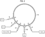
- FIG. 2 is a transverse plan view showing a positional relationship between a manifold and gas supply pipes in the vertical thermal processing apparatus.
- FIGS. 3A to 3C are explanatory views stepwise showing an embodiment of a film forming method according to the present disclosure.
- FIGS. 4D to 4F are explanatory views stepwise showing the embodiment of the film forming method according to the present disclosure.
- the vertical thermal processing apparatus is provided with a reaction tube of a double-tube structure including a cylindrical quartz-made inner tube 11 and a quartz-made outer tube 12 provided so as to surround the inner tube 11 and having a closed upper surface.
- a cylindrical outer casing 13 is provided around the outer tube 12 .
- a heater 14 is provided on an inner peripheral surface of the outer casing 13 .
- the heater 14 is divided into a plurality of regions in the vertical direction, and power control is performed independently for each of the divided height regions.
- the heater 14 is illustrated as a schematic diagram.
- a metallic manifold 15 is provided under the inner tube 11 and the outer tube 12 .
- a reaction container 10 is configured by the inner tube 11 , the outer tube 12 and the manifold 15 .
- Gas supply pipes as gas supply paths opened near the bottom portion of the inner tube 11 are provided in a lower portion of the manifold 15 .
- the gas supply pipes there are provided a gas supply pipe 2 for performing film formation on the wafers W which will be described later, gas supply pipes 31 and 32 for coating the bottom portion of the reaction container 10 , a cleaning gas supply pipe 4 and a gas supply pipe 5 for purging the interior of the reaction container 10 .
- the respective gas supply pipes 2 , 31 , 32 , 4 and 5 are arranged along a circumferential direction of the manifold 15 as shown in FIG. 2 .
- a polysilicon (Si) film is formed on the wafer W, and the bottom portion of the reaction container 10 is coated with a silicon oxide film (SiO 2 film).
- a gas used for forming the polysilicon film may include a monosilane (SiH 4 ) gas, a dichlorosilane (SiH 2 Cl 2 ) gas and the like.
- a base end of the gas supply pipe 2 is connected to a monosilane gas supply source 2 a .
- Examples of a gas used for coating with the silicon oxide film may include a silane gas having an amino group, for example, an aminosilane gas (SiH 3 (NH 2 )), and an oxidizing gas, for example, an ozone (O 3 ) gas.
- a silane gas having an amino group for example, an aminosilane gas (SiH 3 (NH 2 ))
- an oxidizing gas for example, an ozone (O 3 ) gas.
- Base ends of the gas supply pipes 31 and 32 are connected to an aminosilane gas supply source 31 a and an ozone (O 3 ) gas supply source 32 a , respectively.
- a fluorine (F 2 ) gas is used as a cleaning gas for cleaning the interior of the reaction container 10 .
- a base end of the gas supply pipe 4 is connected to a fluorine gas supply source 4 a .
- a nitrogen (N 2 ) gas is used as the purge gas.
- a base end of the gas supply pipe 5 is connected to a nitrogen gas supply source 5 a.
- Each of the gas supply sources 2 a , 31 a , 32 a , 4 a and 5 a shown in FIG. 1 includes a gas cylinder, and a gas supply control device such as a valve and a flow meter. Each of the gas supply control devices is controlled by a control signal provided from a control part 100 composed of a computer.
- One end of an exhaust pipe 16 opened to the external atmosphere of the outer tube 12 is connected to an upper region of the manifold 15 .
- the other end of the exhaust pipe 16 is connected to a vacuum pump 16 c as a vacuum evacuation mechanism via a pressure regulation valve 16 a and a valve 16 b .
- the pressure regulation valve 16 a and the valve 16 b are controlled by the control part 100 .
- the vertical thermal processing apparatus further includes a lid (cap) 6 for opening and closing an opening formed at the lower end of the reaction container 10 (a lower end opening of the manifold 15 ).
- the lid 6 is fixedly provided on a boat elevator 61 as an elevating stand.
- the lid 6 is provided with an auxiliary heater which is a heating part (not shown).
- a rotating shaft 62 is vertically provided in the central portion of the lid 6 .
- the rotating shaft 62 is rotated around a vertical axis by a rotation mechanism 63 provided in the boat elevator 61 .
- a rotary table 64 is provided at the top of the rotating shaft 62 .
- a quartz-made wafer boat 65 as a substrate holder for holding a plurality of wafers W as target substrates in a shelf shape, is mounted on the rotary table 64 .
- a heat insulating unit for thermally insulating a processing atmosphere for example, a heat insulating unit 66 constituted by stacking ring-shaped quartz plates 66 b on a frame body 66 a in a shelf shape, is provided between the wafer boat 65 and the lid 6 .
- the heat insulating unit 66 may also be referred to as a heat insulating part for thermally insulating the processing atmosphere from the outside.
- Software for controlling a series of operations of the vertical thermal processing apparatus is installed in a program storage part (not shown) of the control part 100 via a storage medium such as a compact disk, a hard disk, an MO disk (magneto-optical disk), a memory card, or the like.
- a storage medium such as a compact disk, a hard disk, an MO disk (magneto-optical disk), a memory card, or the like.
- the wafer boat 65 which holds a plurality of, e.g., 100 wafers W in a shelf shape is loaded into the reaction container 10 by the upward movement of the boat elevator 61 .
- the interior of the reaction container 10 is evacuated by the vacuum pump 16 c via the exhaust pipe 16 .
- the temperature of the processing atmosphere of the reaction container 10 (the atmosphere in the region where the wafers W are disposed) is increased to a processing temperature of, for example, 620 degrees C. by the heater 14 .
- a silane-based gas for example, a monosilane gas, which is a processing gas, is supplied into the reaction container 10 from the gas supply pipe 2 .
- the monosilane gas is discharged to the vicinity of the bottom portion of the reaction container 10 and then moved upward while being heated.
- a polysilicon film is formed on the wafer W by a CVD-based reaction.
- the wafer boat 65 is being rotated.
- the supply of the monosilane gas is stopped and, for example, the supply of electric power to the heater 14 is stopped.
- a nitrogen gas as a purge gas is supplied from the nitrogen gas supply pipe 5 into the reaction container 10 .
- a hydrogen gas may be added at the same time.
- the wafer boat 65 is moved down by the boat elevator 61 and is unloaded from the lower end opening of the reaction container 10 to a loading area. Then, for example, five wafers W are taken out from the wafer boat 65 by a transfer mechanism provided in the loading area and are transferred to a holding shelf.
- the (empty) wafer boat 65 in which the wafers W are not mounted is moved upward by the boat elevator 61 and is loaded into the reaction container 10 .
- the lower end opening of the reaction container 10 is closed by the lid 6 .
- a fluorine (F 2 ) gas as a cleaning gas is supplied from the gas supply pipe 4 into the reaction container 10 to remove the polysilicon film formed on the inner wall of the reaction container 10 and the inner surfaces of the wafer boat 65 and the lid 6 .
- the internal pressure of the reaction container 10 is set to, for example, 500 to 1,000 Pa.
- the internal temperature of the reaction container 10 is set to a temperature selected from a range of, for example, 300 to 350 degrees C.
- the inner surface of the lid 6 is heated to, for example, 300 degrees C. by, for example, the auxiliary heater (not shown) provided in the lid 6 as described above, thereby preventing liquefaction of the fluorine gas.
- FIGS. 3A and 4F schematically show the state of the apparatus, the state of the inner surface of the lid 6 and the state of the inner surface near the lower portion of the reaction container 10 in the respective steps performed by the vertical thermal processing apparatus. Since the temperature of the inner surface of the lid 6 is, for example, 350 degrees C., no polysilicon film is formed on the inner surface of the lid 6 in the film forming step as shown in the middle portion of FIG. 3A . A polysilicon film of a slight thickness is formed on the inner surface of the manifold 15 close to the lower portion of the reaction container 10 , for example, the lowermost wafer W in the wafer boat 65 . This state is shown in the lower portion of FIG. 3A .
- reference numeral 10 a indicated in the lower portion denotes a section near the lower portion of the reaction container 10 , which is referred to as a “bottom inner face.”
- Reference numeral 70 denotes the polysilicon film.
- a coating step is performed in which a silicon oxide film (SiO 2 film) is formed inside the reaction container 10 by so-called ALD (Atomic Layer Deposition) using an aminosilane (SiH 3 (NH 2 )) gas as a coating gas and an ozone (O 3 ) gas as an oxidizing gas, which are supplied from the gas supply pipes 31 and 32 , respectively. That is to say, a step of supplying the aminosilane gas, a step of supplying a nitrogen gas as a purge gas into the reaction container 10 and evacuating the interior of the reaction container 10 to replace an atmosphere, a step of supplying the ozone gas, and the aforementioned replacement step are repeated a plurality of times.
- ALD Atomic Layer Deposition
- the aminosilane gas is adsorbed inside the reaction container 10 and is then oxidized by the ozone gas to form a molecular layer of silicon oxide which is a reaction product.
- the molecular layers thus formed are stacked up.
- the internal pressure of the reaction container 10 at the time of supplying the raw material gas and supplying the oxidizing gas in the coating step is, for example, 70 Pa.
- the internal temperature of the reaction container 10 is set to a temperature selected from, for example, 250 to 400 degrees C. In this example, the interior of the reaction container 10 is heated at the same temperature (e.g., 300 degrees C.) as that in the cleaning step by the auxiliary heater provided in the lid 6 .
- the silicon oxide film 71 is also coated (formed) on the bottom inner surface 10 a of the reaction container 10 and the inner surface of the lid 6 .
- the film thickness of the silicon oxide film 71 is set to, for example, 10 nm. Therefore, as shown in FIG. 3C , the particles P 1 are fixed by the silicon oxide film 71 and come into an immovable state.
- the interior of the reaction container 10 is replaced with the nitrogen gas and is returned to atmospheric pressure.
- the wafer boat 65 is moved down and is unloaded from the reaction container 10 .
- the wafers W as target substrates to be processed subsequently are transferred to the wafer boat 65 by the transfer mechanism.
- the wafer boat 65 is moved upward and is loaded into the reaction container 10 .
- the polysilicon film is formed as described above. Thereafter, the same steps as described above are repeated.
- FIGS. 4D to 4F show the state of a series of steps following the step shown in FIG. 3C .
- a polysilicon film forming step as shown in FIG. 4D , the polysilicon film 70 is formed on the silicon oxide film 71 of the bottom inner surface 10 a of the reaction container 10 . Then, in a cleaning step, the polysilicon film 70 is removed. However, particles adhere to the inner surface of the lid 6 and the bottom inner surface 10 a .
- FIG. 4E for the sake of convenience in illustration, there is shown a state in which particles P 2 adhere to the inner surface of the lid 6 and the bottom inner surface 10 a . Furthermore, a silicon oxide film is formed (coated), and a silicon oxide film 72 is coated on the particles P 1 and P 2 . Therefore, the particles P 2 are fixed by the silicon oxide film 72 .
- the particles sequentially adhering to the inner surface of the lid 6 and the bottom inner surface 10 a of the reaction container 10 in this manner are fixed by the silicon oxide film 72 and come into an immovable state.
- the series of steps described above is executed by the software including a process recipe stored in a memory of the control part 100 .
- a film is formed on the bottom portion inside the reaction container in a state in which the wafers W are not present inside the reaction container 10 , so that the particles adhering to the bottom portion including the inner surface of the lid 6 are fixed by the silicon oxide film. Therefore, even if an airflow is generated by the pressure difference between the inside and the outside of the reaction container 10 when the lid 6 is opened, the particles are less likely to move upward. It is therefore possible to reduce particle contamination on the wafers W.
- the operator does not need to clean the inner surface of the lid 6 to remove particles or the frequency of work is reduced. Therefore, it is possible to alleviate the burden on the operator and to suppress a decrease in the operation rate of the apparatus.
- the cleaning step and the coating step can be performed, for example, at the same temperature. Therefore, it is possible to immediately perform the coating step without changing the internal temperature of the reaction container 10 after the cleaning step. This makes it possible to suppress a reduction in throughput which may otherwise be caused by the addition of the coating step.
- the selectivity between the polysilicon film and the silicon oxide film is large. Therefore, there is also an advantage that the coated particles are less likely to scatter again.
- the coating step will now be described.
- a thin film be formed (deposited) on the bottom portion of the reaction container 10 in addition to the inner surface of the lid 6 .
- the temperature of the inner surface of the manifold 15 corresponding to the bottom portion of the reaction container 10 is about 400 degrees C. at a maximum even when the auxiliary heater is provided in the lid 6 .
- the temperature of the inner surface of the lid 6 is further lower and is, for example, 300 to 350 degrees C.
- TEOS tetraethoxysilane
- process capable of forming a film is not limited to being able to form a film with the same film thickness as that in the processing atmosphere inside the reaction container 10 .
- a film thickness of the thin film formed on the substrate arranged in the processing atmosphere is TS and a film thickness of the thin film formed on the inner surface of the lid 6 is TB
- the film thickness TB of the thin film formed on the inner surface of the lid 6 may be 10% or more of the film thickness TS of the thin film formed in the processing atmosphere.
- the numerical value of 10% mentioned above is one example of a value which may be assumed from the viewpoint of effectively fixing the particles adhering to the inner surface of the lid 6 and the viewpoint of not remarkably reducing the throughput as the time period of the coating step becomes too long.
- the present disclosure is a technique of fixing particles by performing the coating step which is a process different from the film forming process performed on the wafer W. Therefore, the above ratio [(TB/TS) ⁇ 100%] is not limited to 10% or more.
- the ratio of TS to TB may be 20% or more, especially 30% or more.
- the coating step may be effective depending on the operation of the apparatus.
- Such a coating step may include an example in which a silicon nitride (Si 2 N 3 ) film is formed by an ALD method using, for example, a dichlorosilane (SiH 2 Cl 2 ) gas and an ammonia gas. In this case, the above ratio is substantially 4 to 6%.
- the ALD is performed using the aminosilane gas and the ozone gas.
- CVD may be performed by simultaneously supplying the aminosilane gas and the ozone gas into the reaction container 10 .
- the Si-containing gas which is a raw material gas is not limited to aminosilane and aminodisilane but may be dichlorosilane [DCS], monosilane (SiH 4 ), disilane (Si 2 H 6 ), hexachlorodisilane (Si 2 Cl 6 ) [HCD], hexamethyldisilazane [HMDS], trichlorosilane (SiHCl 3 ) [TCS], disilylamine [DSA], trisilylamine [TSA], bis(tertiary-butylamino)silane [BTBAS], ((CH 3 ) 3 SiH) [trimethyl silane], ((CH 3 ) 3 SiN 3
- the film forming process used in the coating step may be a process of forming an aluminum oxide (Al 2 O 3 ) film using TMA (trimethylaluminum) and an ozone gas, or a process of forming a hafnium oxide (HfO 2 ) film using TDMAH (tetrakisdimethylamide hafnium) and an ozone gas.
- the aluminum oxide film may be formed, for example, at a temperature ranging room temperature to 500 degrees C.
- the hafnium oxide film may be formed, for example, at a temperature ranging from 200 to 300 degrees C.
- the above ratio related to the aluminum oxide film and the hafnium oxide film is 50% or more. That is to say, the film is formed on the inner surface of the lid 6 with a film thickness of one half or more of the film thickness of the film formed on the wafer.
- the film formation performed on the wafer W may be a step of using the aforementioned ALD method in which a raw material gas and a reaction gas are alternately supplied into the reaction container 10 .
- the thin film formed on the wafer W is not limited to the polysilicon film but may be, for example, a silicon oxide film or a silicon nitride film.
- the silicon oxide film may be formed by, for example, using TEOS as a raw material and supplying an oxygen gas or an ozone gas as an oxidizing gas into the reaction container 10 .
- the gases used in both the film forming step and the coating step are the same in terms of the oxidizing gas, the combinations of the gases used for film formation are different from each other.
- the gases used in both the film forming step and the coating step are different from each other.
- the cleaning step has been described to be performed each time (every time) when the film forming process is performed on the wafer W
- the cleaning step may be performed after the film forming process on the wafer W is performed a plurality of times, for example, after the film forming process on the wafer W is repeatedly performed until an accumulated film thickness reaches a set film thickness.
- the coating step may be performed each time when the cleaning step is performed, or may be performed every time.
- the coating step may be performed in a state in which the wafer boat 65 is not present inside the reaction container 10 , or may be performed in a state in which, as in the above-described embodiment, the wafers W subjected to film formation are transferred from the wafer boat 65 and the empty wafer boat 65 is loaded into the reaction container 10 .
- the configuration in which the gas is supplied to the wafer W is not limited to the configuration in which the gas supply pipes are opened in the bottom portion of the reaction container 10 as in the above-described embodiment.
- a gas supply pipe is arranged in the vertical direction to extend along the wafer boat 65 from the bottom portion of the reaction container 10 and a gas is discharged from a plurality of gas discharge holes formed in the gas supply pipe along the vertical direction, for example, a plurality of gas discharge holes respectively formed at the height positions corresponding to the respective wafers W mounted on the wafer boat 65 .
- This example is an example in which a gas nozzle called a distribution injector or the like is used.
- the supply of the gas for coating is not limited to the configuration in which the gas supply pipes are opened in the bottom portion of the reaction container 10 , the distribution injector may be used.
- the temperature of the processing atmosphere may be lowered, and only the bottom portion of the reaction container 10 may be heated to a temperature for performing the coating.
- a film is formed on a bottom portion of a reaction container in a state in which a target substrate is not present in the reaction container, so that particles on the bottom portion including an inner surface of a lid are fixed. Therefore, it is possible to reduce particle contamination of the target substrate.
Abstract
Description
Claims (7)
Applications Claiming Priority (2)
| Application Number | Priority Date | Filing Date | Title |
|---|---|---|---|
| JP2017066088A JP2018170387A (en) | 2017-03-29 | 2017-03-29 | Film growth method and vertical type thermal processing device |
| JP2017-066088 | 2017-03-29 |
Publications (2)
| Publication Number | Publication Date |
|---|---|
| US20180286665A1 US20180286665A1 (en) | 2018-10-04 |
| US10573518B2 true US10573518B2 (en) | 2020-02-25 |
Family
ID=63671726
Family Applications (1)
| Application Number | Title | Priority Date | Filing Date |
|---|---|---|---|
| US15/933,760 Active US10573518B2 (en) | 2017-03-29 | 2018-03-23 | Film forming method and vertical thermal processing apparatus |
Country Status (3)
| Country | Link |
|---|---|
| US (1) | US10573518B2 (en) |
| JP (1) | JP2018170387A (en) |
| KR (1) | KR102239199B1 (en) |
Families Citing this family (1)
| Publication number | Priority date | Publication date | Assignee | Title |
|---|---|---|---|---|
| KR102359596B1 (en) * | 2021-04-21 | 2022-02-08 | 주식회사 알씨테크 | A seal cap and a semiconductor manufacturing equipment comprising thereof |
Citations (3)
| Publication number | Priority date | Publication date | Assignee | Title |
|---|---|---|---|---|
| US20060216941A1 (en) * | 2003-04-22 | 2006-09-28 | Kazuhide Hasebe | Method for removing silicon oxide film and processing apparatus |
| US20100210094A1 (en) * | 2009-02-19 | 2010-08-19 | Tokyo Electron Limited | Method for using apparatus configured to form germanium-containing film |
| US20100212581A1 (en) * | 2009-02-20 | 2010-08-26 | Tokyo Electron Limited | Silicon film formation apparatus and method for using same |
Family Cites Families (6)
| Publication number | Priority date | Publication date | Assignee | Title |
|---|---|---|---|---|
| JP4897159B2 (en) * | 2001-08-03 | 2012-03-14 | 株式会社日立国際電気 | Manufacturing method of semiconductor device |
| JP5202372B2 (en) * | 2008-03-14 | 2013-06-05 | 東京エレクトロン株式会社 | Metal contamination reduction method for film forming apparatus, semiconductor device manufacturing method, storage medium, and film forming apparatus |
| KR100949358B1 (en) * | 2008-07-25 | 2010-03-26 | 형제산업(주) | Air roll unit for container car |
| WO2011111498A1 (en) * | 2010-03-08 | 2011-09-15 | 株式会社日立国際電気 | Method for producing semiconductor device and substrate treatment device |
| JP5632687B2 (en) * | 2010-09-10 | 2014-11-26 | 株式会社日立国際電気 | Semiconductor device manufacturing method and substrate processing apparatus |
| JP6011420B2 (en) * | 2013-03-29 | 2016-10-19 | 東京エレクトロン株式会社 | Operation method of vertical heat treatment apparatus, vertical heat treatment apparatus and storage medium |
-
2017
- 2017-03-29 JP JP2017066088A patent/JP2018170387A/en active Pending
-
2018
- 2018-03-22 KR KR1020180033120A patent/KR102239199B1/en active IP Right Grant
- 2018-03-23 US US15/933,760 patent/US10573518B2/en active Active
Patent Citations (4)
| Publication number | Priority date | Publication date | Assignee | Title |
|---|---|---|---|---|
| US20060216941A1 (en) * | 2003-04-22 | 2006-09-28 | Kazuhide Hasebe | Method for removing silicon oxide film and processing apparatus |
| US20100210094A1 (en) * | 2009-02-19 | 2010-08-19 | Tokyo Electron Limited | Method for using apparatus configured to form germanium-containing film |
| US20100212581A1 (en) * | 2009-02-20 | 2010-08-26 | Tokyo Electron Limited | Silicon film formation apparatus and method for using same |
| JP2010219494A (en) | 2009-02-20 | 2010-09-30 | Tokyo Electron Ltd | Vertical heat processing device and heat processing method |
Also Published As
| Publication number | Publication date |
|---|---|
| US20180286665A1 (en) | 2018-10-04 |
| JP2018170387A (en) | 2018-11-01 |
| KR102239199B1 (en) | 2021-04-09 |
| KR20180110601A (en) | 2018-10-10 |
Similar Documents
| Publication | Publication Date | Title |
|---|---|---|
| US10312078B2 (en) | Nitride film forming method and storage medium | |
| US9895727B2 (en) | Method of manufacturing semiconductor device, method of cleaning interior of process chamber, substrate processing apparatus, and recording medium | |
| US9441294B2 (en) | Substrate processing apparatus, method of manufacturing semiconductor device and non-transitory computer-readable recording medium | |
| US9076649B2 (en) | Film forming method and apparatus | |
| US8956984B2 (en) | Method of manufacturing semiconductor device, method of processing substrate, substrate processing apparatus, and non-transitory computer-readable recording medium | |
| US7758920B2 (en) | Method and apparatus for forming silicon-containing insulating film | |
| US8257789B2 (en) | Film formation method in vertical batch CVD apparatus | |
| KR101860203B1 (en) | Method of manufacturing semiconductor device, substrate processing apparatus, storage medium and program | |
| US7883581B2 (en) | Substrate processing apparatus and method of manufacturing semiconductor device | |
| US20150031216A1 (en) | Cleaning method, method of manufacturing semiconductor device, substrate processing apparatus, and recording medium | |
| KR101786889B1 (en) | Method of manufacturing semiconductor device, substrate processing apparatus and computer program | |
| US10774421B2 (en) | Semiconductor device manufacturing method, substrate processing apparatus and recording medium | |
| CN111564388B (en) | Substrate processing apparatus, method for manufacturing semiconductor device, and storage medium | |
| US20130252434A1 (en) | Method of manufacturing semiconductor device, method of processing substrate, substrate processing apparatus, and recording medium | |
| WO2018088003A1 (en) | Manufacturing method for semiconductor device, substrate processing device, and program | |
| CN116825609A (en) | Method for manufacturing semiconductor device, substrate processing apparatus, and recording medium | |
| US10854449B2 (en) | Method and apparatus for forming silicon film | |
| JP6011420B2 (en) | Operation method of vertical heat treatment apparatus, vertical heat treatment apparatus and storage medium | |
| US20210180185A1 (en) | Substrate processing apparatus, method of manufacturing semiconductor device, and recording medium | |
| US9972486B2 (en) | Nitride film forming method and storage medium | |
| US10573518B2 (en) | Film forming method and vertical thermal processing apparatus | |
| US10781515B2 (en) | Film-forming method and film-forming apparatus | |
| JP6475135B2 (en) | Semiconductor device manufacturing method, gas supply method, substrate processing apparatus, and substrate holder | |
| JP2023101578A (en) | Method for manufacturing semiconductor device, program, and apparatus and method for processing substrate | |
| KR20200117027A (en) | Semiconductor device manufacturing method, substrate processing device, and recording medium |
Legal Events
| Date | Code | Title | Description |
|---|---|---|---|
| FEPP | Fee payment procedure |
Free format text: ENTITY STATUS SET TO UNDISCOUNTED (ORIGINAL EVENT CODE: BIG.); ENTITY STATUS OF PATENT OWNER: LARGE ENTITY |
|
| AS | Assignment |
Owner name: TOKYO ELECTRON LIMITED, JAPAN Free format text: ASSIGNMENT OF ASSIGNORS INTEREST;ASSIGNOR:FURUSAWA, YOSHIKAZU;REEL/FRAME:045359/0391 Effective date: 20180315 |
|
| STPP | Information on status: patent application and granting procedure in general |
Free format text: NON FINAL ACTION MAILED |
|
| STPP | Information on status: patent application and granting procedure in general |
Free format text: RESPONSE TO NON-FINAL OFFICE ACTION ENTERED AND FORWARDED TO EXAMINER |
|
| STPP | Information on status: patent application and granting procedure in general |
Free format text: EX PARTE QUAYLE ACTION MAILED |
|
| STPP | Information on status: patent application and granting procedure in general |
Free format text: NOTICE OF ALLOWANCE MAILED -- APPLICATION RECEIVED IN OFFICE OF PUBLICATIONS |
|
| STPP | Information on status: patent application and granting procedure in general |
Free format text: PUBLICATIONS -- ISSUE FEE PAYMENT VERIFIED |
|
| STCF | Information on status: patent grant |
Free format text: PATENTED CASE |
|
| CC | Certificate of correction | ||
| MAFP | Maintenance fee payment |
Free format text: PAYMENT OF MAINTENANCE FEE, 4TH YEAR, LARGE ENTITY (ORIGINAL EVENT CODE: M1551); ENTITY STATUS OF PATENT OWNER: LARGE ENTITY Year of fee payment: 4 |