US10564496B2 - Array substrate and manufacturing method thereof and display device - Google Patents
Array substrate and manufacturing method thereof and display device Download PDFInfo
- Publication number
- US10564496B2 US10564496B2 US15/219,647 US201615219647A US10564496B2 US 10564496 B2 US10564496 B2 US 10564496B2 US 201615219647 A US201615219647 A US 201615219647A US 10564496 B2 US10564496 B2 US 10564496B2
- Authority
- US
- United States
- Prior art keywords
- light
- shielding part
- layer
- light shielding
- transparent
- Prior art date
- Legal status (The legal status is an assumption and is not a legal conclusion. Google has not performed a legal analysis and makes no representation as to the accuracy of the status listed.)
- Expired - Fee Related, expires
Links
Images


Classifications
-
- G—PHYSICS
- G02—OPTICS
- G02F—OPTICAL DEVICES OR ARRANGEMENTS FOR THE CONTROL OF LIGHT BY MODIFICATION OF THE OPTICAL PROPERTIES OF THE MEDIA OF THE ELEMENTS INVOLVED THEREIN; NON-LINEAR OPTICS; FREQUENCY-CHANGING OF LIGHT; OPTICAL LOGIC ELEMENTS; OPTICAL ANALOGUE/DIGITAL CONVERTERS
- G02F1/00—Devices or arrangements for the control of the intensity, colour, phase, polarisation or direction of light arriving from an independent light source, e.g. switching, gating or modulating; Non-linear optics
- G02F1/01—Devices or arrangements for the control of the intensity, colour, phase, polarisation or direction of light arriving from an independent light source, e.g. switching, gating or modulating; Non-linear optics for the control of the intensity, phase, polarisation or colour
- G02F1/13—Devices or arrangements for the control of the intensity, colour, phase, polarisation or direction of light arriving from an independent light source, e.g. switching, gating or modulating; Non-linear optics for the control of the intensity, phase, polarisation or colour based on liquid crystals, e.g. single liquid crystal display cells
- G02F1/133—Constructional arrangements; Operation of liquid crystal cells; Circuit arrangements
- G02F1/136—Liquid crystal cells structurally associated with a semi-conducting layer or substrate, e.g. cells forming part of an integrated circuit
- G02F1/1362—Active matrix addressed cells
- G02F1/136209—Light shielding layers, e.g. black matrix, incorporated in the active matrix substrate, e.g. structurally associated with the switching element
-
- G—PHYSICS
- G02—OPTICS
- G02F—OPTICAL DEVICES OR ARRANGEMENTS FOR THE CONTROL OF LIGHT BY MODIFICATION OF THE OPTICAL PROPERTIES OF THE MEDIA OF THE ELEMENTS INVOLVED THEREIN; NON-LINEAR OPTICS; FREQUENCY-CHANGING OF LIGHT; OPTICAL LOGIC ELEMENTS; OPTICAL ANALOGUE/DIGITAL CONVERTERS
- G02F1/00—Devices or arrangements for the control of the intensity, colour, phase, polarisation or direction of light arriving from an independent light source, e.g. switching, gating or modulating; Non-linear optics
- G02F1/01—Devices or arrangements for the control of the intensity, colour, phase, polarisation or direction of light arriving from an independent light source, e.g. switching, gating or modulating; Non-linear optics for the control of the intensity, phase, polarisation or colour
- G02F1/13—Devices or arrangements for the control of the intensity, colour, phase, polarisation or direction of light arriving from an independent light source, e.g. switching, gating or modulating; Non-linear optics for the control of the intensity, phase, polarisation or colour based on liquid crystals, e.g. single liquid crystal display cells
- G02F1/133—Constructional arrangements; Operation of liquid crystal cells; Circuit arrangements
- G02F1/1333—Constructional arrangements; Manufacturing methods
- G02F1/1335—Structural association of cells with optical devices, e.g. polarisers or reflectors
- G02F1/133509—Filters, e.g. light shielding masks
- G02F1/133514—Colour filters
- G02F1/133516—Methods for their manufacture, e.g. printing, electro-deposition or photolithography
-
- G—PHYSICS
- G02—OPTICS
- G02F—OPTICAL DEVICES OR ARRANGEMENTS FOR THE CONTROL OF LIGHT BY MODIFICATION OF THE OPTICAL PROPERTIES OF THE MEDIA OF THE ELEMENTS INVOLVED THEREIN; NON-LINEAR OPTICS; FREQUENCY-CHANGING OF LIGHT; OPTICAL LOGIC ELEMENTS; OPTICAL ANALOGUE/DIGITAL CONVERTERS
- G02F1/00—Devices or arrangements for the control of the intensity, colour, phase, polarisation or direction of light arriving from an independent light source, e.g. switching, gating or modulating; Non-linear optics
- G02F1/01—Devices or arrangements for the control of the intensity, colour, phase, polarisation or direction of light arriving from an independent light source, e.g. switching, gating or modulating; Non-linear optics for the control of the intensity, phase, polarisation or colour
- G02F1/13—Devices or arrangements for the control of the intensity, colour, phase, polarisation or direction of light arriving from an independent light source, e.g. switching, gating or modulating; Non-linear optics for the control of the intensity, phase, polarisation or colour based on liquid crystals, e.g. single liquid crystal display cells
- G02F1/133—Constructional arrangements; Operation of liquid crystal cells; Circuit arrangements
- G02F1/136—Liquid crystal cells structurally associated with a semi-conducting layer or substrate, e.g. cells forming part of an integrated circuit
- G02F1/1362—Active matrix addressed cells
- G02F1/1368—Active matrix addressed cells in which the switching element is a three-electrode device
-
- H01L27/1248—
-
- H01L27/1262—
-
- H—ELECTRICITY
- H10—SEMICONDUCTOR DEVICES; ELECTRIC SOLID-STATE DEVICES NOT OTHERWISE PROVIDED FOR
- H10D—INORGANIC ELECTRIC SEMICONDUCTOR DEVICES
- H10D86/00—Integrated devices formed in or on insulating or conducting substrates, e.g. formed in silicon-on-insulator [SOI] substrates or on stainless steel or glass substrates
- H10D86/01—Manufacture or treatment
- H10D86/021—Manufacture or treatment of multiple TFTs
- H10D86/0212—Manufacture or treatment of multiple TFTs comprising manufacture, treatment or coating of substrates
-
- H—ELECTRICITY
- H10—SEMICONDUCTOR DEVICES; ELECTRIC SOLID-STATE DEVICES NOT OTHERWISE PROVIDED FOR
- H10D—INORGANIC ELECTRIC SEMICONDUCTOR DEVICES
- H10D86/00—Integrated devices formed in or on insulating or conducting substrates, e.g. formed in silicon-on-insulator [SOI] substrates or on stainless steel or glass substrates
- H10D86/40—Integrated devices formed in or on insulating or conducting substrates, e.g. formed in silicon-on-insulator [SOI] substrates or on stainless steel or glass substrates characterised by multiple TFTs
- H10D86/451—Integrated devices formed in or on insulating or conducting substrates, e.g. formed in silicon-on-insulator [SOI] substrates or on stainless steel or glass substrates characterised by multiple TFTs characterised by the compositions or shapes of the interlayer dielectrics
-
- H—ELECTRICITY
- H10—SEMICONDUCTOR DEVICES; ELECTRIC SOLID-STATE DEVICES NOT OTHERWISE PROVIDED FOR
- H10D—INORGANIC ELECTRIC SEMICONDUCTOR DEVICES
- H10D86/00—Integrated devices formed in or on insulating or conducting substrates, e.g. formed in silicon-on-insulator [SOI] substrates or on stainless steel or glass substrates
- H10D86/40—Integrated devices formed in or on insulating or conducting substrates, e.g. formed in silicon-on-insulator [SOI] substrates or on stainless steel or glass substrates characterised by multiple TFTs
- H10D86/60—Integrated devices formed in or on insulating or conducting substrates, e.g. formed in silicon-on-insulator [SOI] substrates or on stainless steel or glass substrates characterised by multiple TFTs wherein the TFTs are in active matrices
-
- G—PHYSICS
- G02—OPTICS
- G02F—OPTICAL DEVICES OR ARRANGEMENTS FOR THE CONTROL OF LIGHT BY MODIFICATION OF THE OPTICAL PROPERTIES OF THE MEDIA OF THE ELEMENTS INVOLVED THEREIN; NON-LINEAR OPTICS; FREQUENCY-CHANGING OF LIGHT; OPTICAL LOGIC ELEMENTS; OPTICAL ANALOGUE/DIGITAL CONVERTERS
- G02F1/00—Devices or arrangements for the control of the intensity, colour, phase, polarisation or direction of light arriving from an independent light source, e.g. switching, gating or modulating; Non-linear optics
- G02F1/01—Devices or arrangements for the control of the intensity, colour, phase, polarisation or direction of light arriving from an independent light source, e.g. switching, gating or modulating; Non-linear optics for the control of the intensity, phase, polarisation or colour
- G02F1/13—Devices or arrangements for the control of the intensity, colour, phase, polarisation or direction of light arriving from an independent light source, e.g. switching, gating or modulating; Non-linear optics for the control of the intensity, phase, polarisation or colour based on liquid crystals, e.g. single liquid crystal display cells
- G02F1/133—Constructional arrangements; Operation of liquid crystal cells; Circuit arrangements
- G02F1/136—Liquid crystal cells structurally associated with a semi-conducting layer or substrate, e.g. cells forming part of an integrated circuit
- G02F1/1362—Active matrix addressed cells
- G02F1/136222—Colour filters incorporated in the active matrix substrate
-
- G—PHYSICS
- G02—OPTICS
- G02F—OPTICAL DEVICES OR ARRANGEMENTS FOR THE CONTROL OF LIGHT BY MODIFICATION OF THE OPTICAL PROPERTIES OF THE MEDIA OF THE ELEMENTS INVOLVED THEREIN; NON-LINEAR OPTICS; FREQUENCY-CHANGING OF LIGHT; OPTICAL LOGIC ELEMENTS; OPTICAL ANALOGUE/DIGITAL CONVERTERS
- G02F1/00—Devices or arrangements for the control of the intensity, colour, phase, polarisation or direction of light arriving from an independent light source, e.g. switching, gating or modulating; Non-linear optics
- G02F1/01—Devices or arrangements for the control of the intensity, colour, phase, polarisation or direction of light arriving from an independent light source, e.g. switching, gating or modulating; Non-linear optics for the control of the intensity, phase, polarisation or colour
- G02F1/13—Devices or arrangements for the control of the intensity, colour, phase, polarisation or direction of light arriving from an independent light source, e.g. switching, gating or modulating; Non-linear optics for the control of the intensity, phase, polarisation or colour based on liquid crystals, e.g. single liquid crystal display cells
- G02F1/133—Constructional arrangements; Operation of liquid crystal cells; Circuit arrangements
- G02F1/136—Liquid crystal cells structurally associated with a semi-conducting layer or substrate, e.g. cells forming part of an integrated circuit
- G02F1/1362—Active matrix addressed cells
- G02F1/136227—Through-hole connection of the pixel electrode to the active element through an insulation layer
-
- G—PHYSICS
- G02—OPTICS
- G02F—OPTICAL DEVICES OR ARRANGEMENTS FOR THE CONTROL OF LIGHT BY MODIFICATION OF THE OPTICAL PROPERTIES OF THE MEDIA OF THE ELEMENTS INVOLVED THEREIN; NON-LINEAR OPTICS; FREQUENCY-CHANGING OF LIGHT; OPTICAL LOGIC ELEMENTS; OPTICAL ANALOGUE/DIGITAL CONVERTERS
- G02F1/00—Devices or arrangements for the control of the intensity, colour, phase, polarisation or direction of light arriving from an independent light source, e.g. switching, gating or modulating; Non-linear optics
- G02F1/01—Devices or arrangements for the control of the intensity, colour, phase, polarisation or direction of light arriving from an independent light source, e.g. switching, gating or modulating; Non-linear optics for the control of the intensity, phase, polarisation or colour
- G02F1/13—Devices or arrangements for the control of the intensity, colour, phase, polarisation or direction of light arriving from an independent light source, e.g. switching, gating or modulating; Non-linear optics for the control of the intensity, phase, polarisation or colour based on liquid crystals, e.g. single liquid crystal display cells
- G02F1/133—Constructional arrangements; Operation of liquid crystal cells; Circuit arrangements
- G02F1/136—Liquid crystal cells structurally associated with a semi-conducting layer or substrate, e.g. cells forming part of an integrated circuit
- G02F1/1362—Active matrix addressed cells
- G02F1/136231—Active matrix addressed cells for reducing the number of lithographic steps
-
- G02F2001/136222—
-
- G02F2001/136231—
-
- G—PHYSICS
- G02—OPTICS
- G02F—OPTICAL DEVICES OR ARRANGEMENTS FOR THE CONTROL OF LIGHT BY MODIFICATION OF THE OPTICAL PROPERTIES OF THE MEDIA OF THE ELEMENTS INVOLVED THEREIN; NON-LINEAR OPTICS; FREQUENCY-CHANGING OF LIGHT; OPTICAL LOGIC ELEMENTS; OPTICAL ANALOGUE/DIGITAL CONVERTERS
- G02F2203/00—Function characteristic
- G02F2203/01—Function characteristic transmissive
-
- G—PHYSICS
- G02—OPTICS
- G02F—OPTICAL DEVICES OR ARRANGEMENTS FOR THE CONTROL OF LIGHT BY MODIFICATION OF THE OPTICAL PROPERTIES OF THE MEDIA OF THE ELEMENTS INVOLVED THEREIN; NON-LINEAR OPTICS; FREQUENCY-CHANGING OF LIGHT; OPTICAL LOGIC ELEMENTS; OPTICAL ANALOGUE/DIGITAL CONVERTERS
- G02F2203/00—Function characteristic
- G02F2203/05—Function characteristic wavelength dependent
-
- G—PHYSICS
- G02—OPTICS
- G02F—OPTICAL DEVICES OR ARRANGEMENTS FOR THE CONTROL OF LIGHT BY MODIFICATION OF THE OPTICAL PROPERTIES OF THE MEDIA OF THE ELEMENTS INVOLVED THEREIN; NON-LINEAR OPTICS; FREQUENCY-CHANGING OF LIGHT; OPTICAL LOGIC ELEMENTS; OPTICAL ANALOGUE/DIGITAL CONVERTERS
- G02F2203/00—Function characteristic
- G02F2203/15—Function characteristic involving resonance effects, e.g. resonantly enhanced interaction
Definitions
- the present application relates to the field of display technology, and particularly to an array substrate, a manufacturing method of the array substrate and a display device comprising the array substrate.
- color filter substrate is required to achieve color display.
- Most of the color filter substrates are realized by providing a light filtering layer including color filters on the base substrate, which may decrease the brightness of the display panels.
- An object of the present invention is to provide an array substrate, a manufacturing method of the array substrate and a display device comprising the array substrate, wherein the display device comprising the array substrate can realize color display without decreasing the brightness.
- an array substrate which is divided into a plurality of pixel units, wherein each pixel unit is provided therein with a light filtering structure
- the light filtering structure includes a first light shielding part and a second light shielding part, which are provided in a thickness direction of the array substrate and spaced apart
- the first light shielding part is provided below the second light shielding part
- the second light shielding part includes a second light shielding part body and a light transmitting hole penetrating through the second light shielding part body along a thickness direction thereof
- the first light shielding part is provided below the light transmitting hole
- a light transmitting gap exists between an inner boundary of an orthographic projection of the second light shielding part body on a layer in which the first light shielding part is provided and a boundary of the first light shielding part
- a transparent light transmitting space is formed above the first light shielding part, and the light transmitting gap allows light with a predetermined wavelength to transmit therethrough.
- the array substrate is divided into a plurality of pixel unit groups, each of which includes three pixel units, light transmitting gaps of the three pixel units of each pixel unit group are arranged so that lights transmitting through the light transmitting gaps are red light, green light and blue light, respectively.
- the light filtering structure includes a transparent light filtering layer formed with a light filtering groove, the first light shielding part is provided in the light filtering groove and at bottom thereof, the second light shielding part body is provided on an upper surface of the transparent light filtering layer, and at least one portion of the light transmitting space is provided in the light filtering groove.
- the pixel unit is provided therein with a thin film transistor, the second light shielding part body and a source and a drain of the thin film transistor are provided in a same layer and are made of a same material.
- a portion of the second light shielding part body is integrated with the drain of the thin film transistor.
- the thin film transistor is of a bottom-gate structure
- an active layer of the thin film transistor is made of an oxide material
- the transparent light filtering layer is provided between the active layer of the thin film transistor and a layer in which the source is provided.
- the transparent light filtering layer is made of silicon oxide and/or aluminium oxide.
- the array substrate further comprises a passivation layer and pixel electrodes, the passivation layer is provided above the layer in which the source and the drain are provided, and each pixel electrode is provided above the passivation layer and electrically connected with a corresponding drain via a through hole.
- the array substrate further comprises a planarization layer, which is provided above the passivation layer, the pixel electrodes are provided on the planarization layer, and the through hole connecting the pixel electrode and the corresponding drain penetrates through the planarization layer and the passivation layer.
- the transparent light filtering layer has a thickness ranging from 40 nm to 120 nm.
- the first light shielding part is made of a metal material.
- a manufacturing method of above array substrate the manufacturing method comprises steps of:
- the base substrate is divided into a plurality of pixel units
- the step of providing the base substrate comprises steps of: providing a transparent base;
- the first light shielding part is provided in a corresponding light filtering groove and at bottom thereof, and the second light shielding part body is provided on an upper surface of the transparent light filtering layer.
- the step of providing the base substrate further comprises the following steps performed prior to the step of forming the transparent light filtering material layer above the transparent base:
- the step of providing the base substrate further comprises the following steps performed after the step of forming the transparent light filtering material layer above the transparent base:
- the sources and initial drains are connected with corresponding active layers through the source through holes and the drain through holes, respectively, wherein the step of forming the pattern including the second light shielding part and the step of forming the pattern including the sources and the initial drains are performed simultaneously.
- the active layers are made of an oxide material.
- the transparent light filtering material layer is made of silicon oxide or aluminium oxide.
- the manufacturing method further comprises the following steps performed after the step of forming the pattern including the sources and the initial drains:
- etching the initial drains to form the light transmitting holes a boundary of the light transmitting hole exceeds a boundary of a corresponding second groove, and a gap between the boundary of the light transmitting hole and the boundary of the corresponding second groove is the light transmitting gap;
- each light filtering groove is aligned with the first groove and the second groove;
- the manufacturing method further comprises a step of:
- the manufacturing method further comprises a following step performed between the step of forming the first light shielding part and the step of forming the pattern including the plurality of pixel electrodes:
- a display device comprising the above array substrate.
- emergent light can have a predetermined wavelength, and the transparent light transmitting space above the first light shielding part forms a resonant cavity, light emerged from the light transmitting gap enters into the light transmitting space to generate a microcavity effect, thus the brightness is increased. Therefore, when the display device including the array substrate performs color display, the brightness of light cannot be decreased, facilitating to reduce the energy consumption.
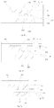
- FIG. 1 is a diagram of an array substrate provided by the present invention.
- FIG. 2 a to FIG. 2 i illustrates a flowchart of a manufacturing method of the array substrate provided by the present invention.
- orientation terms “above” and “below” herein refer to the directions “upper” and “down” in FIG. 1 .
- an array substrate As an aspect of the present invention, as shown in FIG. 1 , there is provided an array substrate, the array substrate is divided into a plurality of pixel units, wherein each pixel unit is provided therein with a light filtering structure, the light filtering structure includes a first light shielding part 130 and a second light shielding part, which are provided in a thickness direction of the array substrate and spaced apart, the first light shielding part 130 is provided below the second light shielding part, the second light shielding part includes a second light shielding part body 162 and a light transmitting hole 163 penetrating through the second light shielding part body 162 along a thickness direction of the second light shielding part body 162 , the first light shielding part 130 is provided below the light transmitting hole 163 , a light transmitting gap exists between an inner boundary of an orthographic projection of the second light shielding part body 162 on a layer in which the first light shielding part 130 is provided and a boundary of the first light shielding part 130 , a transparent light transmitting space
- the light transmitting gap between the inner boundary of the second light shielding part body 162 and the boundary of the first light shielding part 130 is the grating, therefore, diffraction light transmitting through the light transmitting gap may be emerged at a predetermined emergence angle by setting a width of the light transmitting gap, thus the emergent light has a predetermined wavelength (that is, a predetermined color).
- the emergent light may have a predetermined wavelength, and the transparent light transmitting space 180 above the first light shielding part 130 forms a resonant cavity, the emergent light from the light transmitting gap enters into the transparent light transmitting space 180 to generate a microcavity effect, the brightness is increased. Therefore, when color display is realized by using the display device comprising the array substrate described herein, the brightness will not be decreased, facilitating to reduce the energy consumption.
- the array substrate comprises a plurality of pixel unit groups, each of which includes three pixel units, light transmitting gaps of the three pixel units of each pixel unit group are different from each other. Specifically, in a pixel unit group, the light transmitting gaps of the three pixel units are set so that lights emerged from the light transmitting gaps of the three pixel units are red light, green light and blue light respectively.
- the light filtering structure may include a transparent light filtering layer 150 formed with a light filtering groove, the first light shielding part 130 is provided in the light filtering groove and at bottom thereof, the second light shielding part body 162 is provided on an upper surface of the transparent light filtering layer 150 , and at least one portion of the light transmitting space 180 is provided in the light filtering groove.
- a removing method may be used. The removing method will be described in detail hereinafter and will not be described here.
- the pixel unit is provided therein with a thin film transistor.
- the second light shielding part body 162 and a source 161 and a drain of the thin film transistor are provide in a same layer and are made of a same material, thus simplifying the manufacturing process of the array substrate and decreasing the number of masks used in manufacturing the array substrate.
- a portion of the second light shielding part body 162 is integrated with the drain of the thin film transistor, therefore, a structure of the mask for forming the source 161 , the drain and the second light shielding part body 162 can be simplified.
- the thin film transistor is of a bottom-gate structure.
- the thin film transistor may also be of a top-gate structure.
- an active layer 140 of the thin film transistor is made of an oxide material, and the transparent light filtering layer 150 is provided between the active layer 140 of the thin film transistor and a layer in which the source 161 is provided. As shown in the figures, the source 161 and the drain are connected with the active layer 140 via through holes penetrating through the transparent light filtering layer 150 , respectively.
- the transparent light filtering layer 150 may also be used as an etching stop layer for preventing the active layer 140 from being damaged during formations of the source and the drain.
- the active layer 140 may be made of IGZO.
- the transparent light filtering layer 150 there is no specific limitation on the material of the transparent light filtering layer 150 , as long as light can transmit therethrough.
- the transparent light filtering layer 150 is made of silicon oxide and/or aluminium oxide.
- the array substrate further comprises a passivation layer 170 and a pixel electrode 200 , the passivation layer 170 is provided above the layer in which the source 162 and the drain are provided, the pixel electrodes 200 is formed above the passivation layer 170 and electrically connected with a corresponding drain via a through hole.
- the pixel electrode 200 may be directly provided on the passivation layer 170 .
- a planarization layer 190 may further be provided above the passivation layer 170 , and then the pixel electrode 200 is provided on the planarization layer 190 , the through hole connecting the pixel electrode 200 and the corresponding drain penetrates through the planarization layer 190 and the passivation layer 170 .
- the passivation layer 170 there is no specific limitation on the thickness of the passivation layer 170 , and preferably, the passivation layer 170 has a thickness ranging from 200 nm to 400 nm.
- the transparent light filtering layer 150 has a thickness ranging from 40 nm to 120 nm.
- the first light shielding part 130 is made of a metal material.
- a manufacturing method of above array substrate comprises steps of:
- the base substrate is divided into a plurality of pixel units
- each pixel unit is provide therein with a first light shielding part 130 ;
- each pixel unit is provide therein with a second light shielding part body 162 , in a same pixel unit, the first light shielding part 130 and the second light shielding part body 162 are provided in a thickness direction of the array substrate and spaced apart, a light transmitting gap exists between an inner boundary of an orthographic projection of the second light shielding part body 162 on a layer in which the first light shielding part 130 is provided and a boundary of the first light shielding part 130 , a transparent light transmitting space 180 is formed above the first light shielding part 130 , and the light transmitting gap allows light with a predetermined wavelength to transmit therethrough.
- the base substrate is a portion of the array substrate.
- the first light shielding part 130 , the second light shielding part and the transparent light transmitting space form the light filtering structure in the array substrate.
- the light transmitting gap allows light with a predetermined wavelength to transmit therethrough, so that the display device comprising the array substrate described herein can perform color display.
- the step of forming the pattern including the plurality of first light shielding parts there is no specific limitation on order of the step of forming the pattern including the plurality of first light shielding parts and the step of forming the pattern including the plurality of second light shielding parts, as long as the light filtering structure can be obtained.
- the first light shielding parts may be formed on the base substrate first, then a transparent spacing layer is formed, and then the second light shielding parts are formed on the transparent spacing layer.
- a preferable embodiment of the present invention discloses an implementation in which the second light shielding parts are formed prior to the formation of the first light shielding parts, which will be described in detail later and will not be described here.
- the step of providing the base substrate comprises steps of:
- each first light shielding part 130 is provided in a corresponding light filtering groove and at bottom thereof, and the second light shielding part body 162 is provided on an upper surface of the transparent light filtering layer 150 .
- the transparent light filtering material layer may be made of silicon oxide and/or aluminium oxide.
- the transparent light filtering material layer may be made by using PECVD method.
- the light filtering grooves may be formed from the transparent light filtering material layer by using a dry etching method so as to obtain the transparent light filtering layer 150 .
- the transparent base 100 is required to be cleaned so as to remove impurities on a surface of the transparent base.
- the step of providing the base substrate further comprises the following steps performed prior to the step of forming the transparent light filtering material layer above the transparent base:
- the step of providing the base substrate further comprises the following steps performed after the step of forming the transparent light filtering material layer above the transparent base:
- the sources 161 and initial drains are connected with corresponding active layers 140 through the source through holes and the drain through holes, respectively, wherein the step of forming the pattern including the second light shielding part body 162 and the step of forming the pattern including the sources and the initial drains are performed simultaneously.
- the initial drain may be a drain itself, and may also be a structure formed before the drain is formed.
- the pattern including the sources and the initial drains may be made of any one of Mo, MoW and AlNd.
- the pattern including the sources, the initial drains and the first light shielding parts may be formed by using a sputtering method.
- the step of forming the pattern including the gates 110 there is no specific limitation on the step of forming the pattern including the gates 110 .
- the pattern including the gates 110 may be formed by using a conventional photolithography patterning process.
- the step of forming the pattern including the gates 110 may comprise:
- etching the metal material layer by using a wet etching or a dry etching method, so as to obtain the pattern including the gates 110 .
- the gates 110 may be made of aluminium.
- the thickness of the gate 110 for facilitating molding, preferably, the gate may have a thickness of 220 nm.
- the gate insulation layer 120 may be made of silicon dioxide. As a specific embodiment, the gate insulation layer 120 may be obtained by using a CVD method. In the present invention, the gate insulation layer 120 may have a thickness ranging from 200 nm to 500 nm.
- the sources 161 , the drains and the second light shielding part bodies 162 may be obtained by a same patterning process, and therefore, the manufacturing method provided by the present invention is simple and low in cost.
- the drain in a pixel unit is integrated with the second light shielding part body 162 in the pixel unit.
- the active layer 110 may be made of an oxide material.
- the transparent light filtering layer 150 may also be used as an etching stop layer.
- the transparent light filtering material layer may be made of silicon oxide and/or aluminium oxide.
- the active layer 110 may be made of IGZO.
- an IGZO layer may be formed by depositing using a sputtering method, then a patterning process may be performed thereon to obtain the pattern including the active layer 110 .
- the IGZO layer may have a thickness ranging from 10 nm to 80 nm.
- the first light shielding part 130 is formed after the formation of the second light shielding part body 162 will be described.
- the manufacturing method further comprises the following steps performed after the step of forming the pattern including the sources and the initial drains:
- a position of the first groove a corresponds to that of the first light shielding part 130 , as shown in FIG. 2 c;
- the light filtering groove d is aligned with the first groove a and the second groove b, as shown in FIG. 2 f;
- first shielding material layer by depositing, the first shielding material falling within the light filtering groove c forms the first light shielding part 130 , as shown in FIG. 2 g;
- the first shielding material layer above the remained photoresist layer is also removed, thus saving an etching process and simplifying the manufacturing method.
- the passivation layer has a thickness ranging from 200 nm to 400 nm.
- the passivation layer 170 may be made of silicon oxide or silicon nitride, and specifically, the passivation layer 170 may be formed by using a PECVD method.
- the manufacturing method comprises: forming a pattern including a plurality of pixel electrodes 200 , each pixel unit is provided therein with a pixel electrode 200 , which is connected with a corresponding drain via a through hole penetrating through the passivation layer 170 .
- the pixel electrodes 200 may be directly formed on the passivation layer 170 .
- the pixel electrode 200 is made of a pixel electrode material with low fluidity (for example, ITO or IZO),
- a planarization layer may be provided above the passivation layer 170 first, then a pixel electrode material layer may be formed by sputtering, wherein the pixel electrode material layer has a thickness ranging from 40 nm to 135 nm. After the pixel electrode material layer is formed, the pixel electrodes 200 are formed by a pattering process.
- the manufacturing method further comprises a step performed between the step of forming the first light shielding part 130 and the step of forming the pattern including the plurality of pixel electrodes 200 :
- the material of the transparent light filtering material layer includes silicon oxide and/or aluminium oxide.
- the transparent light filtering material layer has a thickness ranging from 40 nm to 120 nm.
- a display device comprising the array substrate provided by the present invention.
- the light filtering structure of the array substrate has a light transmitting gap, so that light transmitted through the light transmitting gap has a predetermined wavelength, and the transparent light transmitting space of the light filtering structure generates a microcavity effect, the brightness of the emergent light is increased, and thus it is ensured that the display device can perform color display while lowering the energy consumption.
- the display device may be a liquid crystal display device.
- the display device may be an electronic device such as a mobile phone, a tablet computer, a desk computer and a navigator.
Landscapes
- Physics & Mathematics (AREA)
- Nonlinear Science (AREA)
- Mathematical Physics (AREA)
- Chemical & Material Sciences (AREA)
- Crystallography & Structural Chemistry (AREA)
- General Physics & Mathematics (AREA)
- Optics & Photonics (AREA)
- Engineering & Computer Science (AREA)
- Microelectronics & Electronic Packaging (AREA)
- Manufacturing & Machinery (AREA)
- Devices For Indicating Variable Information By Combining Individual Elements (AREA)
Abstract
Description
Claims (18)
Applications Claiming Priority (3)
| Application Number | Priority Date | Filing Date | Title |
|---|---|---|---|
| CN201610136521.9 | 2016-03-10 | ||
| CN201610136521 | 2016-03-10 | ||
| CN201610136521.9A CN105867006B (en) | 2016-03-10 | 2016-03-10 | Array substrate and its manufacturing method and display device |
Publications (2)
| Publication Number | Publication Date |
|---|---|
| US20170261823A1 US20170261823A1 (en) | 2017-09-14 |
| US10564496B2 true US10564496B2 (en) | 2020-02-18 |
Family
ID=56624590
Family Applications (1)
| Application Number | Title | Priority Date | Filing Date |
|---|---|---|---|
| US15/219,647 Expired - Fee Related US10564496B2 (en) | 2016-03-10 | 2016-07-26 | Array substrate and manufacturing method thereof and display device |
Country Status (2)
| Country | Link |
|---|---|
| US (1) | US10564496B2 (en) |
| CN (1) | CN105867006B (en) |
Families Citing this family (4)
| Publication number | Priority date | Publication date | Assignee | Title |
|---|---|---|---|---|
| CN107170829A (en) * | 2017-05-15 | 2017-09-15 | 京东方科技集团股份有限公司 | A kind of thin film transistor and its manufacturing method, array substrate and display panel |
| CN108227230B (en) * | 2018-02-05 | 2021-01-22 | 京东方科技集团股份有限公司 | A collimation structure, its manufacturing method and display device |
| CN110504275B (en) * | 2018-05-17 | 2021-11-12 | 京东方科技集团股份有限公司 | Array substrate, manufacturing method thereof, display panel and display device |
| CN111092109B (en) * | 2020-01-02 | 2022-04-08 | 武汉天马微电子有限公司 | Display panel and display device |
Citations (4)
| Publication number | Priority date | Publication date | Assignee | Title |
|---|---|---|---|---|
| CN1319195A (en) | 1999-07-07 | 2001-10-24 | 松下电器产业株式会社 | Liquid crystal display device and method for manufacturing the same |
| US20030137622A1 (en) | 1999-09-13 | 2003-07-24 | Lg, Philips Lcd Co., Ltd. | Liquid crystal display device and method of manufacturing the same |
| US20080094554A1 (en) | 2006-10-20 | 2008-04-24 | Hitachi Displays, Ltd. | Liquid crystal display unit |
| CN105116651A (en) | 2015-09-01 | 2015-12-02 | 深圳市华星光电技术有限公司 | Boa type liquid crystal panel |
-
2016
- 2016-03-10 CN CN201610136521.9A patent/CN105867006B/en not_active Expired - Fee Related
- 2016-07-26 US US15/219,647 patent/US10564496B2/en not_active Expired - Fee Related
Patent Citations (6)
| Publication number | Priority date | Publication date | Assignee | Title |
|---|---|---|---|---|
| CN1319195A (en) | 1999-07-07 | 2001-10-24 | 松下电器产业株式会社 | Liquid crystal display device and method for manufacturing the same |
| US6727965B1 (en) * | 1999-07-07 | 2004-04-27 | Matsushita Electric Industrial Co., Ltd. | Semitransparent liquid crystal display device |
| US20030137622A1 (en) | 1999-09-13 | 2003-07-24 | Lg, Philips Lcd Co., Ltd. | Liquid crystal display device and method of manufacturing the same |
| US20080094554A1 (en) | 2006-10-20 | 2008-04-24 | Hitachi Displays, Ltd. | Liquid crystal display unit |
| CN105116651A (en) | 2015-09-01 | 2015-12-02 | 深圳市华星光电技术有限公司 | Boa type liquid crystal panel |
| US9874796B2 (en) | 2015-09-01 | 2018-01-23 | Shenzhen China Star Optoelectronics Technology Co., Ltd. | BOA liquid crystal panel |
Non-Patent Citations (2)
| Title |
|---|
| Office Action dated Aug. 14, 2018 issued in corresponding Chinese Application No. 201610136521.9. |
| The Second Office Action dated Jan. 11, 2019 corresponding to Chinese application No. 201610136521.9. |
Also Published As
| Publication number | Publication date |
|---|---|
| US20170261823A1 (en) | 2017-09-14 |
| CN105867006A (en) | 2016-08-17 |
| CN105867006B (en) | 2019-08-06 |
Similar Documents
| Publication | Publication Date | Title |
|---|---|---|
| US20210335940A1 (en) | Display device, display substrate and manufacturing method of display substrate | |
| US10205121B2 (en) | Organic electroluminescent display panel and display apparatus | |
| US9709864B2 (en) | Array substrate and its manufacturing method and display device | |
| CN104460147B (en) | Thin-film transistor array base-plate, manufacture method and display device | |
| US20170200773A1 (en) | Method for Manufacturing Display Substrate, Display Substrate and Display Device | |
| US20170090229A1 (en) | Semiconductor device, display device and method for manufacturing semiconductor device | |
| US9329445B2 (en) | Mask plate and processes for manufacturing ultraviolet mask plate and array substrate | |
| CN106783883B (en) | Display substrate and preparation method thereof | |
| US10564496B2 (en) | Array substrate and manufacturing method thereof and display device | |
| WO2018120691A1 (en) | Array substrate and method for manufacturing same, and display device | |
| TWI646374B (en) | Display with color mixing prevention structure | |
| US10217773B2 (en) | Array substrate and fabrication method thereof, display panel and fabrication method thereof | |
| JP2016018734A (en) | Display device and method of manufacturing the same | |
| WO2020228425A1 (en) | Array substrate, manufacturing method therefor, display panel, and display device | |
| WO2014015617A1 (en) | Array substrate and display device | |
| WO2013143321A1 (en) | Array substrate and manufacturing method thereof, and display device | |
| US10153305B2 (en) | Array substrate, manufacturing method thereof, and display device | |
| US9933652B2 (en) | Color filter array substrate and manufacturing method thereof, and display device | |
| US11822178B2 (en) | Array substrate, fabrication method thereof, liquid crystal display panel and display device | |
| US20190081087A1 (en) | Stack structure and preparation method thereof | |
| US9494837B2 (en) | Manufacturing method of TFT array substrate, TFT array substrate and display device | |
| US20070153173A1 (en) | Transflective type liquid crystal display and fabricating method | |
| CN106547146A (en) | Dot structure and its manufacture method, array base palte and display device | |
| KR102499080B1 (en) | Organic light emitting diode display device and manufacturing method for the same | |
| CN102830531B (en) | TFT (Thin Film Transistor) array substrate, manufacturing method and liquid crystal display device |
Legal Events
| Date | Code | Title | Description |
|---|---|---|---|
| AS | Assignment |
Owner name: BOE TECHNOLOGY GROUP CO., LTD., CHINA Free format text: ASSIGNMENT OF ASSIGNORS INTEREST;ASSIGNOR:WANG, DONGFANG;REEL/FRAME:039271/0455 Effective date: 20160606 |
|
| STPP | Information on status: patent application and granting procedure in general |
Free format text: RESPONSE TO NON-FINAL OFFICE ACTION ENTERED AND FORWARDED TO EXAMINER |
|
| STPP | Information on status: patent application and granting procedure in general |
Free format text: FINAL REJECTION MAILED |
|
| STPP | Information on status: patent application and granting procedure in general |
Free format text: RESPONSE AFTER FINAL ACTION FORWARDED TO EXAMINER |
|
| STPP | Information on status: patent application and granting procedure in general |
Free format text: NOTICE OF ALLOWANCE MAILED -- APPLICATION RECEIVED IN OFFICE OF PUBLICATIONS |
|
| STPP | Information on status: patent application and granting procedure in general |
Free format text: PUBLICATIONS -- ISSUE FEE PAYMENT RECEIVED |
|
| STCF | Information on status: patent grant |
Free format text: PATENTED CASE |
|
| FEPP | Fee payment procedure |
Free format text: MAINTENANCE FEE REMINDER MAILED (ORIGINAL EVENT CODE: REM.); ENTITY STATUS OF PATENT OWNER: LARGE ENTITY |
|
| LAPS | Lapse for failure to pay maintenance fees |
Free format text: PATENT EXPIRED FOR FAILURE TO PAY MAINTENANCE FEES (ORIGINAL EVENT CODE: EXP.); ENTITY STATUS OF PATENT OWNER: LARGE ENTITY |
|
| STCH | Information on status: patent discontinuation |
Free format text: PATENT EXPIRED DUE TO NONPAYMENT OF MAINTENANCE FEES UNDER 37 CFR 1.362 |
|
| FP | Lapsed due to failure to pay maintenance fee |
Effective date: 20240218 |