US10558287B2 - Pressure-sensitive display touch unit, touch screen, and manufacturing method thereof - Google Patents
Pressure-sensitive display touch unit, touch screen, and manufacturing method thereof Download PDFInfo
- Publication number
- US10558287B2 US10558287B2 US15/103,862 US201415103862A US10558287B2 US 10558287 B2 US10558287 B2 US 10558287B2 US 201415103862 A US201415103862 A US 201415103862A US 10558287 B2 US10558287 B2 US 10558287B2
- Authority
- US
- United States
- Prior art keywords
- lower electrode
- dielectric layer
- driving electrode
- electrode
- touch
- Prior art date
- Legal status (The legal status is an assumption and is not a legal conclusion. Google has not performed a legal analysis and makes no representation as to the accuracy of the status listed.)
- Active, expires
Links
Images

Classifications
-
- G—PHYSICS
- G06—COMPUTING; CALCULATING OR COUNTING
- G06F—ELECTRIC DIGITAL DATA PROCESSING
- G06F3/00—Input arrangements for transferring data to be processed into a form capable of being handled by the computer; Output arrangements for transferring data from processing unit to output unit, e.g. interface arrangements
- G06F3/01—Input arrangements or combined input and output arrangements for interaction between user and computer
- G06F3/03—Arrangements for converting the position or the displacement of a member into a coded form
- G06F3/041—Digitisers, e.g. for touch screens or touch pads, characterised by the transducing means
- G06F3/0416—Control or interface arrangements specially adapted for digitisers
-
- G—PHYSICS
- G06—COMPUTING; CALCULATING OR COUNTING
- G06F—ELECTRIC DIGITAL DATA PROCESSING
- G06F3/00—Input arrangements for transferring data to be processed into a form capable of being handled by the computer; Output arrangements for transferring data from processing unit to output unit, e.g. interface arrangements
- G06F3/01—Input arrangements or combined input and output arrangements for interaction between user and computer
- G06F3/03—Arrangements for converting the position or the displacement of a member into a coded form
- G06F3/041—Digitisers, e.g. for touch screens or touch pads, characterised by the transducing means
- G06F3/0414—Digitisers, e.g. for touch screens or touch pads, characterised by the transducing means using force sensing means to determine a position
-
- G—PHYSICS
- G06—COMPUTING; CALCULATING OR COUNTING
- G06F—ELECTRIC DIGITAL DATA PROCESSING
- G06F3/00—Input arrangements for transferring data to be processed into a form capable of being handled by the computer; Output arrangements for transferring data from processing unit to output unit, e.g. interface arrangements
- G06F3/01—Input arrangements or combined input and output arrangements for interaction between user and computer
- G06F3/03—Arrangements for converting the position or the displacement of a member into a coded form
- G06F3/041—Digitisers, e.g. for touch screens or touch pads, characterised by the transducing means
- G06F3/044—Digitisers, e.g. for touch screens or touch pads, characterised by the transducing means by capacitive means
-
- G—PHYSICS
- G06—COMPUTING; CALCULATING OR COUNTING
- G06F—ELECTRIC DIGITAL DATA PROCESSING
- G06F3/00—Input arrangements for transferring data to be processed into a form capable of being handled by the computer; Output arrangements for transferring data from processing unit to output unit, e.g. interface arrangements
- G06F3/01—Input arrangements or combined input and output arrangements for interaction between user and computer
- G06F3/03—Arrangements for converting the position or the displacement of a member into a coded form
- G06F3/041—Digitisers, e.g. for touch screens or touch pads, characterised by the transducing means
- G06F3/045—Digitisers, e.g. for touch screens or touch pads, characterised by the transducing means using resistive elements, e.g. a single continuous surface or two parallel surfaces put in contact
-
- G—PHYSICS
- G06—COMPUTING; CALCULATING OR COUNTING
- G06F—ELECTRIC DIGITAL DATA PROCESSING
- G06F2203/00—Indexing scheme relating to G06F3/00 - G06F3/048
- G06F2203/041—Indexing scheme relating to G06F3/041 - G06F3/045
- G06F2203/04103—Manufacturing, i.e. details related to manufacturing processes specially suited for touch sensitive devices
-
- G—PHYSICS
- G06—COMPUTING; CALCULATING OR COUNTING
- G06F—ELECTRIC DIGITAL DATA PROCESSING
- G06F2203/00—Indexing scheme relating to G06F3/00 - G06F3/048
- G06F2203/041—Indexing scheme relating to G06F3/041 - G06F3/045
- G06F2203/04104—Multi-touch detection in digitiser, i.e. details about the simultaneous detection of a plurality of touching locations, e.g. multiple fingers or pen and finger
-
- G—PHYSICS
- G06—COMPUTING; CALCULATING OR COUNTING
- G06F—ELECTRIC DIGITAL DATA PROCESSING
- G06F2203/00—Indexing scheme relating to G06F3/00 - G06F3/048
- G06F2203/041—Indexing scheme relating to G06F3/041 - G06F3/045
- G06F2203/04105—Pressure sensors for measuring the pressure or force exerted on the touch surface without providing the touch position
Definitions
- the present invention relates to the technologies of touch control and display screens, and in particular to a pressure-sensitive display screen touch-control unit, a touch screen and a manufacturing method thereof, and a basic sensing unit used in a touch screen.
- touch actions are sensed by capacitors, resistors, surface acoustic wave, optical means or the like.
- Surface acoustic wave touch screen (surface acoustic wave technology) is the only one of existing touch screen technologies in which touch pressure may be sensed.
- the technology due to shortcomings such as being inapplicable to large-size screens, being too sensitive to surface contaminations, being easy to be disrupted by sound, being difficult to achieve multi-point touch and sense static pressure, or the like, cannot be applied to mainstream devices such as mobile phones, tablet computers or the like. Thus, it is hard to become a mainstream technology.
- the capacitive touch screen capable of achieving multi-point touch and having high location sensitivity, is the mainstream touch screen technology at present.
- Touch screens as an important and direct input and output tool for human-machine interaction, are mostly based on two-dimensionality at present. That is, actions of a person who touches the screen in an x-y plane parallel to the screen body may be sensed.
- Applying a touch pressure on an object or on a person is a way for a person to transfer information or emotion, for example, the force applied when playing an instrument, the force applied when painting, explicit expression or implicit expression made in a manner of body touch, or the like.
- pressure sensing becomes a novel human-machine interaction mode. This technology has broad application prospect.
- a main objective of the present invention is to provide a pressure-sensitive display screen touch-control unit, a touch screen and a manufacturing method thereof.
- the touch-control unit With the touch-control unit, external pressure is converted into a current signal such that pressure becomes an information input mode.
- the touch-control unit may also be combined with the existing capacitive touch screen or the resistive touch screen, such that the touch-control unit may be compatible with the existing multi-point touch function, and may also sense change in pressure sensitively.
- functions of the existing touch screens may be enhanced to rich operations and applications of touch screens.
- a pressure-sensitive display screen touch-control unit including a driving electrode, a lower electrode, and a dielectric layer sandwiched between the driving electrode and the lower electrode, a thickness of the dielectric layer being between 0.5 nm and 5 nm.
- C and A are proportional constants
- U 0 is an arithmetic mean value of escape barriers of the driving electrode and the lower electrode
- d is the thickness of the dielectric layer.
- the driving electrode and the lower electrode are transparent or semi-transparent conductors, and are made from any one of indium tin oxide (ITO), aluminum-doped zinc oxide (AZO), fluorine-doped zinc oxide (FTO), gallium-doped zinc oxide (GZO), graphene and metal nanowire array.
- ITO indium tin oxide
- AZO aluminum-doped zinc oxide
- FTO fluorine-doped zinc oxide
- GZO gallium-doped zinc oxide
- graphene graphene and metal nanowire array.
- the dielectric layer is made from polyamide, polyimide, poly(p-phenylene terephthamide), polyurea, aluminum oxide, zirconium oxide, hafnium oxide, silicon dioxide, aluminum alkoxide or Zincone.
- the dielectric layer is manufactured by atomic layer deposition or molecular layer deposition.
- a capacitive touch screen including the pressure-sensitive display screen touch-control unit is provided, wherein an array of the pressure-sensitive display screen touch-control unit is manufactured on a front panel of glass or polymer.
- a resistive touch screen including the pressure-sensitive display screen touch-control unit is provided, wherein an array of the pressure-sensitive display screen touch-control units are manufactured on a soft substrate of the resistive touch screen, and the array is covered by an insulating film.
- a method for manufacturing a pressure-sensitive display screen touch-control unit including: providing a dielectric layer sandwiched between a driving electrode and a lower electrode; and manufacturing the dielectric layer by atomic layer deposition or molecular layer deposition, a thickness of the dielectric layer being between 0.5 nm and 5 nm.
- a method for manufacturing a capacitive touch screen which includes the method for manufacturing the pressure-sensitive display screen touch-control unit is provided, including: manufacturing an array of the pressure-sensitive display screen touch-control unit on a front panel made from glass or a polymer.
- a method for manufacturing a resistive touch screen which includes the method for manufacturing the pressure-sensitive display screen touch-control unit is provided, including: manufacturing an array of the pressure-sensitive display screen touch-control units on a soft substrate of the resistive touch screen; and covering the array with an insulating film.
- the pressure-sensitive display screen touch-control unit, the touch screen, and a manufacturing method thereof, which are provided by the present invention, have the following advantages.
- An external pressure may be converted into a current signal by the display screen touch-control unit, and a touch pressure may be sensed by detecting change in the current signal; in this way, the touch pressure may be sensitively detected just by receiving a touch pressure signal such that pressure may be utilized as an information input mode.
- the display screen touch-control unit may also be compatible with the existing capacitive touch screen and the resistive touch screen, and may be compatible with multi-point touch; by combining the touch-control unit with a capacitive touch screen or a resistive touch screen, not only a multi-point function may be achieved, but also pressure may be sensitively sensed, thereby facilitating the design and realization of highly sensitive touch-control/touch display screen with multiple functions (for example, with a force feedback function).
- FIG. 1 is a schematic structure diagram of a pressure-sensitive display screen touch-control unit according to the present invention
- FIG. 2 is a schematic view of a touch pressure sensor which is compatible with a capacitive touch screen, according to one embodiment of the present invention.
- FIG. 3 is a schematic view of a touch pressure sensor which is compatible with a resistive touch screen, according to one embodiment of the present invention.
- FIG. 1 is a schematic structure diagram of a pressure-sensitive display screen touch-control unit according to the present invention.
- a basic unit of the touch pressure sensor is described therein, which mainly includes an upper electrode (driving electrode) 101 , a lower electrode 102 , and an ultra-thin dielectric layer 103 sandwiched between the upper electrode 101 and the lower electrode 102 .
- the upper electrode 101 and the lower electrode 102 are transparent or semi-transparent conductors, and are made from any one of indium tin oxide (ITO), aluminum-doped zinc oxide (AZO), fluorine-doped zinc oxide (FTO), gallium-doped zinc oxide (GZO), graphene or metal nanowire array.
- ITO indium tin oxide
- AZO aluminum-doped zinc oxide
- FTO fluorine-doped zinc oxide
- GZO gallium-doped zinc oxide
- graphene or metal nanowire array The general film thickness and the manufacturing method thereof are well-known in the field
- the ultra-thin dielectric layer 103 sandwiched between the upper electrode 101 and the lower electrode 102 has a thickness of between 0.5 nm and 5 nm with excellent compactness.
- the dielectric layer 103 (which is a thin film) is manufactured by atomic layer deposition (ALD) or molecular layer deposition (MLD).
- the dielectric layer 103 is made from polyamide, polyimide, poly(p-phenylene terephthamide), polyurea, aluminum oxide, zirconium oxide, hafnium oxide, silicon dioxide, aluminum alkoxide or Zincone.
- the working principle is as follows.
- the dielectric layer 103 is used as a barrier of free electrons in electrodes; since the barrier is ultra-thin, when a pressure is applied between the upper electrode 101 and the lower electrode 102 , according to the principle of quantum mechanics, there is a chance for electrons to pass through the barrier to form a tunnel current I T .
- C and A are proportional constants
- U 0 is an arithmetic mean value of the escape barriers of the driving electrode and the lower electrode
- d is the thickness of the dielectric layer 103 . It may be concluded from the formula that the deformation of the ultra-thin dielectric layer 103 resulted from touch by a finger, that is, subtle changes in thickness d will affect the tunnel current I T exponentially. By detecting change in the tunnel current I T , changes in touch pressure may be detected.
- FIG. 2 is a schematic view of a touch pressure sensor which is compatible with a capacitive touch screen, according to one embodiment of the present invention.
- a driving electrode 201 and a receiving electrode 202 of a traditional capacitive screen are formed on a front panel 205 made from glass or a polymer.
- the driving electrode 201 and the receiving electrode 202 may be made from, but not limited to, ITO, AZO or the like. ITO is preferred in this embodiment, and the manufacturing method and the parameters thereof are well-known in the field of capacitive touch screens.
- a driving pulse signal 207 is imposed on the driving electrode 201 by a driving buffer 206 ; and then charges are collected by a receiving circuit 209 through a receiving electrode 202 to sense touch actions and positions in an x-y plane.
- the dielectric layer 203 is additionally provided below the driving electrode 201 to form an array of the pressure-sensitive display screen touch-control units together with the lower electrode 204 .
- the dielectric layer 203 may be manufactured by atomic layer deposition (ALD) or molecular layer deposition (MLD), and may be made from, but not limited to, polyamide, polyimide, poly(p-phenylene terephthamide) (PPTA), polyurea, aluminum oxide, zirconium oxide, hafnium oxide, silicon dioxide, aluminum alkoxide and Zincone. Polyurea deposited by MLD is preferred in this embodiment; and the film thickness thereof is between 0.5 nm and 3 nm, preferably 1 nm.
- a pressure is applied to the dielectric layer 203 to control the lower electrode 204 by touch.
- a section of the lower electrode 204 is exposed to be connected to a pressure sensing circuit 208 , for sensing a current which is generated on the lower electrode 204 by the driving pulse signal 207 , in order to sense the pressure.
- the lower electrode 204 may be made from, but not limited to, ITO, AZO or the like, preferably ITO; and with the film thickness is 50 nm to 1000 nm, preferably 100 nm.
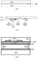
- FIG. 3 is a schematic view of a touch pressure sensor which is compatible with a resistive touch screen, according to one embodiment of the present invention.
- a basic unit of the touch sensor of the present invention is combined with a traditional resistive touch screen to form a first resistive film 304 on a hard substrate 301 of the touch screen; and the basic unit is combined with another soft substrate 302 of the touch screen by an insulating fulcrum 303 .
- a second resistive film 305 is formed at the lowest end of the soft substrate 302 .
- the hard substrate 301 , the soft substrate 302 , the insulating fulcrum 303 , the first resistive film 304 and the second resistive film 305 which are mentioned above, are all manufactured by a well-known method for manufacturing a resistive touch screen. It is different from the traditional resistive touch screen in that: before the second resistive film 305 is formed, first, an array of the second electrode 308 (i.e., the driving electrode) and the ultra-thin dielectric layer 309 is formed on the soft substrate 302 ; and then, the first electrode 307 (i.e., the lower electrode) is formed; and finally, the array is covered by an insulating film 306 .
- the second electrode 308 i.e., the driving electrode
- the ultra-thin dielectric layer 309 is formed on the soft substrate 302 ; and then, the first electrode 307 (i.e., the lower electrode) is formed; and finally, the array is covered by an insulating film 306 .
- the array of the pressure-sensitive display screen touch-control units is formed by the second electrode 308 , the ultra-thin dielectric layer 309 and the first electrode 307 all together.
- the second electrode 308 and the first electrode 307 may be made from, but not limited to, ITO, silver nanowire arrays, poly(3,4-ethylenedioxythiophen):poly(4-styrenesulfoate) (PEDOT:PSS) or the like, and PEDOT:PSS is preferred here; the manufacturing method thereof may be, but not limited to, inkjet printing, plasma polymerization, spin-coating, vapor vacuum deposition or the like, and inkjet printing is preferred here; and the film thickness thereof is preferably 500 nm.
- the insulating film 306 may be manufactured from, but not limited to, polyurea, polyimide, aluminum alkoxide or the like, and polyurea is preferred here; and the film thickness is preferably 0.8 nm and the deposition method is MLD.
Abstract
Description
I T =CV Texp(−AU 0 d);
I T =CV Texp(−AU 0 d)
Claims (6)
I T =CV T exp(−AU 0 d)
I T =CV T exp(−AU 0 d)
Applications Claiming Priority (4)
| Application Number | Priority Date | Filing Date | Title |
|---|---|---|---|
| CN201310668839.8A CN104714672B (en) | 2013-12-11 | 2013-12-11 | Pressure sensitive display screen touch control unit, touch screen and its manufacturing method |
| CN201310668839 | 2013-12-11 | ||
| CN201310668839.8 | 2013-12-11 | ||
| PCT/CN2014/093571 WO2015085936A1 (en) | 2013-12-11 | 2014-12-11 | Pressure-sensitive display touch unit, touch screen, and manufacturing method thereof |
Publications (2)
| Publication Number | Publication Date |
|---|---|
| US20160334919A1 US20160334919A1 (en) | 2016-11-17 |
| US10558287B2 true US10558287B2 (en) | 2020-02-11 |
Family
ID=53370631
Family Applications (1)
| Application Number | Title | Priority Date | Filing Date |
|---|---|---|---|
| US15/103,862 Active 2034-12-21 US10558287B2 (en) | 2013-12-11 | 2014-12-11 | Pressure-sensitive display touch unit, touch screen, and manufacturing method thereof |
Country Status (6)
| Country | Link |
|---|---|
| US (1) | US10558287B2 (en) |
| EP (1) | EP3082022A4 (en) |
| JP (1) | JP2017503256A (en) |
| KR (1) | KR20160096156A (en) |
| CN (1) | CN104714672B (en) |
| WO (1) | WO2015085936A1 (en) |
Families Citing this family (16)
| Publication number | Priority date | Publication date | Assignee | Title |
|---|---|---|---|---|
| DE102016113162A1 (en) * | 2015-07-28 | 2017-02-02 | Schott Ag | Control panel for a household appliance with at least one user interface, home appliance and method for producing the control panel with user interface |
| CN106502481A (en) * | 2015-09-08 | 2017-03-15 | 深圳莱宝高科技股份有限公司 | A kind of touch control display apparatus and preparation method thereof |
| CN105183230B (en) | 2015-09-18 | 2017-09-19 | 京东方科技集团股份有限公司 | A kind of display device, pressure detection method and pressure-detecting device |
| KR101781273B1 (en) * | 2015-12-15 | 2017-09-25 | 연세대학교 산학협력단 | Input device using highly sensitive pressure sensor |
| DE102015120168A1 (en) | 2015-11-09 | 2017-05-11 | Schott Ag | Two-dimensional sensor arrangement |
| CN105930001B (en) * | 2016-04-19 | 2019-03-01 | 京东方科技集团股份有限公司 | Touch panel and preparation method thereof and display device |
| CN105784254A (en) * | 2016-04-20 | 2016-07-20 | 南方科技大学 | Flexible pressure sensor and touch screen |
| TWI607362B (en) * | 2016-08-15 | 2017-12-01 | 友達光電股份有限公司 | Sensing device and detecting method |
| US10649595B2 (en) * | 2017-03-03 | 2020-05-12 | Atmel Corporation | Touch sensor with force sensor response normalization, and related method and apparatus |
| WO2019004752A1 (en) * | 2017-06-30 | 2019-01-03 | 동우 화인켐 주식회사 | Force touch sensor |
| CN108052220B (en) * | 2017-12-06 | 2021-11-26 | 京东方科技集团股份有限公司 | Display module, manufacturing method thereof, display device and wearable device |
| EP3714772A1 (en) * | 2019-03-29 | 2020-09-30 | Picosun Oy | Sensor and its manufacturing method |
| WO2020209452A1 (en) * | 2019-04-09 | 2020-10-15 | (주)에프티씨 | Capacitive and resistive touch film |
| CN111411346A (en) * | 2020-04-14 | 2020-07-14 | 西安近代化学研究所 | Flexible inorganic-organic composite water vapor oxygen barrier film and low-temperature preparation method thereof |
| US11507240B2 (en) * | 2020-04-20 | 2022-11-22 | Higgstec Inc. | Touch sensor |
| CN114027797A (en) * | 2021-11-19 | 2022-02-11 | 惠州Tcl移动通信有限公司 | Skin detection processing method and device based on touch screen, mobile terminal and medium |
Citations (33)
| Publication number | Priority date | Publication date | Assignee | Title |
|---|---|---|---|---|
| JPH02253117A (en) | 1989-03-28 | 1990-10-11 | Seiko Instr Inc | Sensor and minute pressure change detecting method |
| US20060214918A1 (en) * | 2003-08-11 | 2006-09-28 | Destura Galileo J A | Touch sensitive display |
| EP1708291A2 (en) | 2005-03-31 | 2006-10-04 | TDK Corporation | Tunneling effect element and physical quantity to electrical quantity transducer |
| JP2006294864A (en) | 2005-04-11 | 2006-10-26 | Seiko Epson Corp | Nonvolatile semiconductor storage device and manufacturing method thereof |
| US20060266282A1 (en) * | 2001-08-09 | 2006-11-30 | Doan Trung T | Variable temperature deposition methods |
| US7234360B2 (en) * | 2002-04-04 | 2007-06-26 | Stifting Caesar | TMR sensor |
| JP2008193096A (en) | 2007-02-06 | 2008-08-21 | Young Joo Oh | Metal capacitor and manufacturing method therefor |
| US20090104455A1 (en) | 2007-10-23 | 2009-04-23 | Miin-Jang Chen | Transparent conductive component utilized in touch panel |
| JP2009244206A (en) | 2008-03-31 | 2009-10-22 | Nissha Printing Co Ltd | Pressure sensitive sensor |
| US20100013784A1 (en) | 2008-07-16 | 2010-01-21 | Nitto Denko Corporation | Transparent conductive film, transparent conductive laminate, touch panel, and method for producing transparent conductive film |
| US20100020041A1 (en) * | 2008-07-23 | 2010-01-28 | Samsung Mobile Display Co., Ltd. | Flat panel display device |
| JP2010505088A (en) | 2006-08-01 | 2010-02-18 | ワシントン ユニヴァーシティー | Multifunctional nanoscopy for imaging cells |
| US20100045630A1 (en) * | 2008-08-19 | 2010-02-25 | Qualcomm Incorporated | Capacitive MEMS-Based Display with Touch Position Sensing |
| CN101846562A (en) | 2009-03-27 | 2010-09-29 | 罗伯特.博世有限公司 | Pressure sensor |
| EP2239651A2 (en) | 2009-03-27 | 2010-10-13 | CSEM Centre Suisse d'Electronique et de Microtechnique SA - Recherche et Développement | Smart Label |
| CN102004573A (en) | 2010-07-28 | 2011-04-06 | 深圳市汇顶科技有限公司 | Touch detection system and detection method thereof |
| WO2011156447A1 (en) | 2010-06-11 | 2011-12-15 | 3M Innovative Properties Company | Positional touch sensor with force measurement |
| US20120062245A1 (en) | 2010-09-10 | 2012-03-15 | Zhenan Bao | Pressure Sensing Apparatuses and Methods |
| US20120120009A1 (en) * | 2009-03-25 | 2012-05-17 | Peratech Limited | Sensor |
| JP2012137972A (en) | 2010-12-27 | 2012-07-19 | Kyocera Corp | Electronic device |
| US20120187368A1 (en) * | 2011-01-20 | 2012-07-26 | West Virginia University | High Sensitivity Stress Sensor Based on Hybrid Materials |
| US20120256865A1 (en) * | 2009-12-22 | 2012-10-11 | Takao Hashimoto | Touch panel and portable device using the same |
| US8325143B2 (en) * | 2003-07-21 | 2012-12-04 | Creator Technology B.V. | Touch sensitive display for a portable device |
| US20120313860A1 (en) * | 2011-06-09 | 2012-12-13 | Akinori Hashimura | Metallic Nanoparticle Pressure Sensor |
| US20130047747A1 (en) | 2011-08-25 | 2013-02-28 | Samsung Electro-Mechanics Co., Ltd. | Capacitive pressure sensor and input device including the same |
| WO2013037425A1 (en) | 2011-09-13 | 2013-03-21 | Albert-Ludwigs-Universität Freiburg | Apparatus for detecting a position of a force |
| CN103329084A (en) | 2010-03-17 | 2013-09-25 | 摩托罗拉解决方案公司 | Transparent force sensor and method of fabrication |
| US20130293482A1 (en) | 2012-05-04 | 2013-11-07 | Qualcomm Mems Technologies, Inc. | Transparent through-glass via |
| US20130307082A1 (en) | 2012-05-16 | 2013-11-21 | Renesas Electronics Corporation | Semiconductor devices with self-aligned source drain contacts and methods for making the same |
| US20130319138A1 (en) * | 2010-11-03 | 2013-12-05 | Robert Bosch Gmbh | Microelectromechanical sensor for measuring a force, and corresponding method |
| US20130333922A1 (en) * | 2011-04-29 | 2013-12-19 | Nissha Printing Co., Ltd. | Spacerless input device |
| US9152289B2 (en) * | 2009-12-11 | 2015-10-06 | Nissha Printing Co., Ltd. | Installation structure of thin-type display and resistive film type touch panel, resistive film type touch panel unit with front-surface protrusions, and thin-type display unit with back-surface protrusions |
| US20150378483A1 (en) * | 2013-02-06 | 2015-12-31 | Fujikura Ltd. | Method for producing pressure detection device, pressure detection device, pressure-sensitive sensor, and electronic device |
-
2013
- 2013-12-11 CN CN201310668839.8A patent/CN104714672B/en active Active
-
2014
- 2014-12-11 US US15/103,862 patent/US10558287B2/en active Active
- 2014-12-11 WO PCT/CN2014/093571 patent/WO2015085936A1/en active Application Filing
- 2014-12-11 EP EP14869005.0A patent/EP3082022A4/en not_active Ceased
- 2014-12-11 JP JP2016537482A patent/JP2017503256A/en active Pending
- 2014-12-11 KR KR1020167018197A patent/KR20160096156A/en not_active Application Discontinuation
Patent Citations (46)
| Publication number | Priority date | Publication date | Assignee | Title |
|---|---|---|---|---|
| JPH02253117A (en) | 1989-03-28 | 1990-10-11 | Seiko Instr Inc | Sensor and minute pressure change detecting method |
| US20060266282A1 (en) * | 2001-08-09 | 2006-11-30 | Doan Trung T | Variable temperature deposition methods |
| US7234360B2 (en) * | 2002-04-04 | 2007-06-26 | Stifting Caesar | TMR sensor |
| US8325143B2 (en) * | 2003-07-21 | 2012-12-04 | Creator Technology B.V. | Touch sensitive display for a portable device |
| US20060214918A1 (en) * | 2003-08-11 | 2006-09-28 | Destura Galileo J A | Touch sensitive display |
| US20060220781A1 (en) | 2005-03-31 | 2006-10-05 | Tdk Corporation | Tunneling effect element and physical quantity to electrical quantity transducer |
| JP2006284208A (en) | 2005-03-31 | 2006-10-19 | Tdk Corp | Tunnel effect element and transformer for physical quantity/electrical quantity |
| CN1841033A (en) | 2005-03-31 | 2006-10-04 | Tdk株式会社 | Tunneling effect element and physical quantity to electrical quantity transducer |
| EP1708291A2 (en) | 2005-03-31 | 2006-10-04 | TDK Corporation | Tunneling effect element and physical quantity to electrical quantity transducer |
| JP2006294864A (en) | 2005-04-11 | 2006-10-26 | Seiko Epson Corp | Nonvolatile semiconductor storage device and manufacturing method thereof |
| JP2010505088A (en) | 2006-08-01 | 2010-02-18 | ワシントン ユニヴァーシティー | Multifunctional nanoscopy for imaging cells |
| US20140197855A1 (en) | 2006-08-01 | 2014-07-17 | Washington University | Multifunctional Nanoscopy for Imaging Cells |
| JP2008193096A (en) | 2007-02-06 | 2008-08-21 | Young Joo Oh | Metal capacitor and manufacturing method therefor |
| US20080285210A1 (en) | 2007-02-06 | 2008-11-20 | Oh Young Joo | Metal capacitor and manufacturing method thereof |
| US20090104455A1 (en) | 2007-10-23 | 2009-04-23 | Miin-Jang Chen | Transparent conductive component utilized in touch panel |
| JP2009244206A (en) | 2008-03-31 | 2009-10-22 | Nissha Printing Co Ltd | Pressure sensitive sensor |
| US20100013784A1 (en) | 2008-07-16 | 2010-01-21 | Nitto Denko Corporation | Transparent conductive film, transparent conductive laminate, touch panel, and method for producing transparent conductive film |
| US20100020041A1 (en) * | 2008-07-23 | 2010-01-28 | Samsung Mobile Display Co., Ltd. | Flat panel display device |
| US20100045630A1 (en) * | 2008-08-19 | 2010-02-25 | Qualcomm Incorporated | Capacitive MEMS-Based Display with Touch Position Sensing |
| US20120120009A1 (en) * | 2009-03-25 | 2012-05-17 | Peratech Limited | Sensor |
| CN101846562A (en) | 2009-03-27 | 2010-09-29 | 罗伯特.博世有限公司 | Pressure sensor |
| EP2239651A2 (en) | 2009-03-27 | 2010-10-13 | CSEM Centre Suisse d'Electronique et de Microtechnique SA - Recherche et Développement | Smart Label |
| US9152289B2 (en) * | 2009-12-11 | 2015-10-06 | Nissha Printing Co., Ltd. | Installation structure of thin-type display and resistive film type touch panel, resistive film type touch panel unit with front-surface protrusions, and thin-type display unit with back-surface protrusions |
| CN103092455A (en) | 2009-12-22 | 2013-05-08 | 日本写真印刷株式会社 | Touch Panel And Portable Device Using Same |
| US20120256865A1 (en) * | 2009-12-22 | 2012-10-11 | Takao Hashimoto | Touch panel and portable device using the same |
| US8482541B2 (en) * | 2009-12-22 | 2013-07-09 | Nissha Printing Co., Ltd. | Touch panel and portable device using the same |
| CN103329084A (en) | 2010-03-17 | 2013-09-25 | 摩托罗拉解决方案公司 | Transparent force sensor and method of fabrication |
| WO2011156447A1 (en) | 2010-06-11 | 2011-12-15 | 3M Innovative Properties Company | Positional touch sensor with force measurement |
| CN102004573A (en) | 2010-07-28 | 2011-04-06 | 深圳市汇顶科技有限公司 | Touch detection system and detection method thereof |
| CN103210457A (en) | 2010-09-10 | 2013-07-17 | 小利兰·斯坦福大学托管委员会 | Pressure sensing apparatuses and methods |
| CN103250218A (en) | 2010-09-10 | 2013-08-14 | 小利兰·斯坦福大学托管委员会 | Interface apparatus and methods |
| US9281415B2 (en) | 2010-09-10 | 2016-03-08 | The Board Of Trustees Of The Leland Stanford Junior University | Pressure sensing apparatuses and methods |
| US20120062245A1 (en) | 2010-09-10 | 2012-03-15 | Zhenan Bao | Pressure Sensing Apparatuses and Methods |
| US9021898B2 (en) * | 2010-11-03 | 2015-05-05 | Robert Bosch Gmbh | Microelectromechanical sensor for measuring a force, and corresponding method |
| US20130319138A1 (en) * | 2010-11-03 | 2013-12-05 | Robert Bosch Gmbh | Microelectromechanical sensor for measuring a force, and corresponding method |
| JP2012137972A (en) | 2010-12-27 | 2012-07-19 | Kyocera Corp | Electronic device |
| US20120187368A1 (en) * | 2011-01-20 | 2012-07-26 | West Virginia University | High Sensitivity Stress Sensor Based on Hybrid Materials |
| US20130333922A1 (en) * | 2011-04-29 | 2013-12-19 | Nissha Printing Co., Ltd. | Spacerless input device |
| US8669952B2 (en) * | 2011-06-09 | 2014-03-11 | Sharp Laboratories Of America, Inc. | Metallic nanoparticle pressure sensor |
| US20120313860A1 (en) * | 2011-06-09 | 2012-12-13 | Akinori Hashimura | Metallic Nanoparticle Pressure Sensor |
| US20130047747A1 (en) | 2011-08-25 | 2013-02-28 | Samsung Electro-Mechanics Co., Ltd. | Capacitive pressure sensor and input device including the same |
| WO2013037425A1 (en) | 2011-09-13 | 2013-03-21 | Albert-Ludwigs-Universität Freiburg | Apparatus for detecting a position of a force |
| US20130293482A1 (en) | 2012-05-04 | 2013-11-07 | Qualcomm Mems Technologies, Inc. | Transparent through-glass via |
| US20130307082A1 (en) | 2012-05-16 | 2013-11-21 | Renesas Electronics Corporation | Semiconductor devices with self-aligned source drain contacts and methods for making the same |
| JP2013239706A (en) | 2012-05-16 | 2013-11-28 | Renesas Electronics Corp | Substituted metal gate transistor and manufacturing method therefor |
| US20150378483A1 (en) * | 2013-02-06 | 2015-12-31 | Fujikura Ltd. | Method for producing pressure detection device, pressure detection device, pressure-sensitive sensor, and electronic device |
Non-Patent Citations (3)
| Title |
|---|
| G Rubio-Bollinger et al: "Carbon-fiber tips for scanning probe microscopes and molecular electronics experiments", Nanoscale Research Letters, 7(2012), May 15, 2012,pp. 1-4, XP055463929, New York. |
| G RUBIO-BOLLINGER, A CASTELLANOS-GOMEZ, S BILAN, L.A ZOTTI, C.R ARROYO, N AGRAÏT, J CUEVAS: "Carbon-fiber tips for scanning probe microscopes and molecular electronics experiments", NANOSCALE RESEARCH LETTERS, 7 (2012), SPRINGEROPEN, NEW YORK, 15 May 2012 (2012-05-15), New York, pages 1 - 4, XP055463929, Retrieved from the Internet <URL:http://www.eng.utah.edu/~lzang/images/Lecture_6_STM.pdf> DOI: 10.1186/1556-276X-7-254 |
| Lu Guo, Basic physics Coursebook vol. two, Sep. 30, 1998, p. 542. |
Also Published As
| Publication number | Publication date |
|---|---|
| EP3082022A1 (en) | 2016-10-19 |
| KR20160096156A (en) | 2016-08-12 |
| CN104714672B (en) | 2019-04-09 |
| CN104714672A (en) | 2015-06-17 |
| JP2017503256A (en) | 2017-01-26 |
| WO2015085936A1 (en) | 2015-06-18 |
| EP3082022A4 (en) | 2016-12-21 |
| US20160334919A1 (en) | 2016-11-17 |
Similar Documents
| Publication | Publication Date | Title |
|---|---|---|
| US10558287B2 (en) | Pressure-sensitive display touch unit, touch screen, and manufacturing method thereof | |
| WO2017045382A1 (en) | Touchscreen and pressure touch control detection method thereof | |
| US9262008B2 (en) | Method of recognizing touch | |
| US20070242054A1 (en) | Light transmission touch panel and manufacturing method thereof | |
| JP2018530820A (en) | Keyboard with adaptive input sequence | |
| TW201508560A (en) | Press detection function-equipped touch panel | |
| US20130335371A1 (en) | Touch device and a detection method thereof | |
| US9547030B2 (en) | Method of recognizing touch | |
| US9647040B2 (en) | Touch display device and manufacturing method thereof | |
| TW201447665A (en) | Touch-control display and fabrication method thereof | |
| CN108509095A (en) | Digitizer and preparation method thereof | |
| US20100231531A1 (en) | Touch panel device | |
| KR102255445B1 (en) | Touch sensor | |
| CN108509075A (en) | Digitizer and preparation method thereof | |
| CN108089741A (en) | Display panel and touch display unit | |
| JP2014081910A (en) | Touch panel and manufacturing method of the same | |
| US9329740B2 (en) | Method of recognizing touch | |
| KR102088769B1 (en) | Method for manufacturing touch screen panel and touch screen panel | |
| KR20140137631A (en) | Transparent electrode pattern structure and touch screen panel having the same | |
| TW201800919A (en) | Transparent electrode and electronic device including the same | |
| KR20150006228A (en) | Touch panel | |
| US20190278399A1 (en) | Input sensor and display device including the same | |
| JP3178844U (en) | Touch control unit | |
| KR20110136050A (en) | Touch screen panel | |
| WO2022105723A1 (en) | Sensing input apparatus and method based on capacitive touch input device |
Legal Events
| Date | Code | Title | Description |
|---|---|---|---|
| AS | Assignment |
Owner name: KUNSHAN GO-VISIONOX OPTO-ELECTRONICS CO., LTD., CHINA Free format text: ASSIGNMENT OF ASSIGNORS INTEREST;ASSIGNORS:ZHU, SHAOPENG;QIU, YONG;CHEN, HONG;AND OTHERS;REEL/FRAME:039002/0126 Effective date: 20160606 Owner name: KUNSHAN NEW FLAT PANEL DISPLAY TECHNOLOGY CENTER CO., LTD., CHINA Free format text: ASSIGNMENT OF ASSIGNORS INTEREST;ASSIGNORS:ZHU, SHAOPENG;QIU, YONG;CHEN, HONG;AND OTHERS;REEL/FRAME:039002/0126 Effective date: 20160606 Owner name: KUNSHAN NEW FLAT PANEL DISPLAY TECHNOLOGY CENTER C Free format text: ASSIGNMENT OF ASSIGNORS INTEREST;ASSIGNORS:ZHU, SHAOPENG;QIU, YONG;CHEN, HONG;AND OTHERS;REEL/FRAME:039002/0126 Effective date: 20160606 Owner name: KUNSHAN GO-VISIONOX OPTO-ELECTRONICS CO., LTD., CH Free format text: ASSIGNMENT OF ASSIGNORS INTEREST;ASSIGNORS:ZHU, SHAOPENG;QIU, YONG;CHEN, HONG;AND OTHERS;REEL/FRAME:039002/0126 Effective date: 20160606 |
|
| STPP | Information on status: patent application and granting procedure in general |
Free format text: FINAL REJECTION MAILED |
|
| STPP | Information on status: patent application and granting procedure in general |
Free format text: DOCKETED NEW CASE - READY FOR EXAMINATION |
|
| STPP | Information on status: patent application and granting procedure in general |
Free format text: NON FINAL ACTION MAILED |
|
| STPP | Information on status: patent application and granting procedure in general |
Free format text: RESPONSE TO NON-FINAL OFFICE ACTION ENTERED AND FORWARDED TO EXAMINER |
|
| STPP | Information on status: patent application and granting procedure in general |
Free format text: NOTICE OF ALLOWANCE MAILED -- APPLICATION RECEIVED IN OFFICE OF PUBLICATIONS |
|
| STPP | Information on status: patent application and granting procedure in general |
Free format text: PUBLICATIONS -- ISSUE FEE PAYMENT RECEIVED |
|
| STCF | Information on status: patent grant |
Free format text: PATENTED CASE |
|
| MAFP | Maintenance fee payment |
Free format text: PAYMENT OF MAINTENANCE FEE, 4TH YEAR, LARGE ENTITY (ORIGINAL EVENT CODE: M1551); ENTITY STATUS OF PATENT OWNER: LARGE ENTITY Year of fee payment: 4 |