US10558002B2 - Optical receiver module, optical module, and optical transmission equipment - Google Patents
Optical receiver module, optical module, and optical transmission equipment Download PDFInfo
- Publication number
- US10558002B2 US10558002B2 US16/365,715 US201916365715A US10558002B2 US 10558002 B2 US10558002 B2 US 10558002B2 US 201916365715 A US201916365715 A US 201916365715A US 10558002 B2 US10558002 B2 US 10558002B2
- Authority
- US
- United States
- Prior art keywords
- optical
- light receiving
- lens
- receiver module
- end part
- Prior art date
- Legal status (The legal status is an assumption and is not a legal conclusion. Google has not performed a legal analysis and makes no representation as to the accuracy of the status listed.)
- Active
Links
Images


Classifications
-
- G—PHYSICS
- G02—OPTICS
- G02B—OPTICAL ELEMENTS, SYSTEMS OR APPARATUS
- G02B6/00—Light guides; Structural details of arrangements comprising light guides and other optical elements, e.g. couplings
- G02B6/24—Coupling light guides
- G02B6/42—Coupling light guides with opto-electronic elements
- G02B6/4201—Packages, e.g. shape, construction, internal or external details
- G02B6/4204—Packages, e.g. shape, construction, internal or external details the coupling comprising intermediate optical elements, e.g. lenses, holograms
- G02B6/4206—Optical features
-
- G—PHYSICS
- G02—OPTICS
- G02B—OPTICAL ELEMENTS, SYSTEMS OR APPARATUS
- G02B6/00—Light guides; Structural details of arrangements comprising light guides and other optical elements, e.g. couplings
- G02B6/24—Coupling light guides
- G02B6/42—Coupling light guides with opto-electronic elements
- G02B6/4201—Packages, e.g. shape, construction, internal or external details
- G02B6/4204—Packages, e.g. shape, construction, internal or external details the coupling comprising intermediate optical elements, e.g. lenses, holograms
- G02B6/4214—Packages, e.g. shape, construction, internal or external details the coupling comprising intermediate optical elements, e.g. lenses, holograms the intermediate optical element having redirecting reflective means, e.g. mirrors, prisms for deflecting the radiation from horizontal to down- or upward direction toward a device
-
- G—PHYSICS
- G02—OPTICS
- G02B—OPTICAL ELEMENTS, SYSTEMS OR APPARATUS
- G02B6/00—Light guides; Structural details of arrangements comprising light guides and other optical elements, e.g. couplings
- G02B6/24—Coupling light guides
- G02B6/42—Coupling light guides with opto-electronic elements
- G02B6/4201—Packages, e.g. shape, construction, internal or external details
- G02B6/4274—Electrical aspects
- G02B6/4284—Electrical aspects of optical modules with disconnectable electrical connectors
-
- G—PHYSICS
- G02—OPTICS
- G02B—OPTICAL ELEMENTS, SYSTEMS OR APPARATUS
- G02B6/00—Light guides; Structural details of arrangements comprising light guides and other optical elements, e.g. couplings
- G02B6/24—Coupling light guides
- G02B6/42—Coupling light guides with opto-electronic elements
- G02B6/4201—Packages, e.g. shape, construction, internal or external details
- G02B6/4249—Packages, e.g. shape, construction, internal or external details comprising arrays of active devices and fibres
- G02B6/425—Optical features
Definitions
- the present invention relates to an optical receiver module, an optical module, and an optical transmission equipment, and in particular relates to a technology for improving the high frequency characteristic.
- the optical receiver module may further be provided with an integrated circuit (IC) having an amplification function represented by a transimpedance amplifier (hereinafter described as TIA).
- IC integrated circuit
- TIA transimpedance amplifier
- the IC is electrically connected to the light receiving element.
- the light receiving element converts the optical signal received into an electric signal, wherein the IC amplifies the electric signal.
- JP 2012-58409 A there is disclosed an optical receiver module having a structure in which an IC with the TIA function is disposed on the same substrate as a light receiving element.
- the optical receiver module described in JP 2015-31818 A has a complicated structure having two lens surfaces.
- the first lens surface collimates the light from the optical fiber
- the mirror reflects the light to change the proceeding direction
- the second lens surface collects the light to make the light reach the light receiving element.
- the length of an interconnection for connecting the IC with the amplification function and the light receiving element cannot be shortened, an increase in the inductance is incurred, and thus, the high frequency characteristic is affected.
- the present invention is made in view of such a problem, and has an object of providing an optical receiver module, an optical module, and an optical transmission equipment each capable of achieving both of an improvement in high frequency characteristic and reduction in size.
- the optical receiver module includes a substrate, an IC disposed on a surface of the substrate, provided with two or more IC terminals disposed along an end part, and having an amplification function, a light receiving element disposed on the surface of the substrate and in front of the IC, provided with two or more PD terminals respectively connected to the two or more IC terminals through two or more wires, and having a light receiving window through which light externally enters the light receiving element, and a first optical component disposed on the surface of the substrate and in front of the IC so as to cover the light receiving element, and provided with two bridge footing sections rising upward from the surface of the substrate, and a lens main body section supported by the two bridge footing sections, and located between upper portions of the two bridge footing sections, the lens main body section has a rising surface disposed in front, and is provided with a lens disposed on the rising surface and adapted to converge light entering the lens, and a mirror adapted to reflect the light converge
- a ratio of the distance L 2 to the distance L 1 may be no lower than 0.07 and lower than 1.0.
- the optical module according to the present invention may include the optical receiver module according to one of (1) and (2) described above, and an optical transmitter module.
- the optical transmission equipment according to the present invention includes the optical module according to (3) described above.
- an optical receiver module an optical module and an optical transmission equipment in which an improvement in high frequency characteristic and reduction in size are both satisfied.
- FIG. 1 is a schematic view illustrating a configuration of an optical transmission equipment and an optical module according to a first embodiment of the present invention.
- FIG. 2 is a schematic view illustrating a structure of an optical receiver module according to the first embodiment of the present invention.
- FIG. 3 is a front view of a microlens array according to the first embodiment of the present invention.
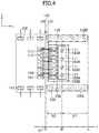
- FIG. 4 is a cross-sectional view illustrating a configuration of a principal part of the optical receiver module according to the first embodiment of the present invention.
- FIG. 5 is a cross-sectional view illustrating a configuration of a principal part of the optical receiver module according to the first embodiment of the present invention.
- FIG. 6 is a cross-sectional view illustrating a configuration of a principal part of an optical receiver module according to a second embodiment of the present invention.
- FIG. 7 is a cross-sectional view illustrating a configuration of a principal part of an optical receiver module according to a third embodiment of the present invention.
- FIG. 8 is a cross-sectional view illustrating a configuration of a principal part of an optical receiver module according to a fourth embodiment of the present invention.
- FIG. 1 is a schematic view illustrating a configuration of an optical transmission equipment 1 and an optical module 2 according to a first embodiment of the present invention.
- the optical transmission equipment 1 includes a printed circuit board 11 (PCB) and an IC 12 .
- the optical transmission equipment 1 is, for example, a large-capacity router or a switch.
- the optical transmission equipment 1 has, for example, a function of a switching equipment, and is disposed in a base station or the like.
- a plurality of optical modules 2 is mounted in the optical transmission equipment 1 .
- the optical transmission equipment 1 acquires data for receiving (electric signal for receiving) from the optical module 2 , determines to transmit what data to where using the IC 12 or the like, generates data for transmitting (electric signal for transmitting), and transmits the data to the corresponding optical module 2 through the printed circuit board 11 .
- the optical module 2 is a transceiver having a function of optical transmitting and a function of optical receiving.
- the optical module 2 includes a printed circuit board 21 , an optical receiver module 23 A which converts an optical signal received through an optical fiber 3 A into an electric signal, and an optical transmitter module 23 B which converts an electric signal into an optical signal and transmits the optical signal to an optical fiber 3 B.
- the printed circuit board 21 is connected to the optical receiver module 23 A and the optical transmitter module 23 B through flexible printed circuits 22 A and 22 B (FPC), respectively.
- An electric signal is transmitted from the optical receiver module 23 A to the printed circuit board 21 through the flexible printed circuit 22 A, and an electric signal is transmitted from the printed circuit board 21 to the optical transmitter module 23 B through the flexible printed circuit 22 B.
- the optical modules 2 and the optical transmission equipment 1 are connected to each other through electrical connectors 5 .
- the optical receiver module 23 A and the optical transmitter module 23 B are electrically connected to the printed circuit board 21 and convert an optical/electric signal into an electric/optical signal.
- the printed circuit board 21 includes a control circuit (for example, an IC) to control the electric signal transmitted from the optical receiver module 23 A, and a control circuit (for example, an IC) to control the electric signal transmitted to the optical transmitter module 23 B.
- a transmission system includes two or more of the optical transmission equipments 1 , two or more of the optical modules 2 , and one or more of optical fibers 3 (not shown in FIG. 1 : for example, the optical fibers 3 A and 3 B).
- One or more of the optical modules 2 are connected to each optical transmission equipment 1 .
- the optical fiber 3 is connected between the optical modules 2 mounted on the two optical transmission equipments 1 , respectively. Transmitting data generated by one of the two optical transmission equipments 1 is converted into an optical signal by the mounted optical module 2 , and such an optical signal is transmitted to the optical fiber 3 .
- the optical signal transmitted over the optical fiber 3 is received by the optical module 2 mounted on the other of the two optical transmission equipments 1 , and the optical module 2 converts the optical signal into an electric signal and transmits the electric signal to the other of the two optical transmission equipments 1 as receiving data.
- FIG. 2 is a schematic view illustrating the structure of an optical receiver module 100 according to the first embodiment.
- the optical receiver module 100 according to the first embodiment corresponds to the optical receiver module 23 A illustrated in FIG. 1 .
- the optical receiver module 100 is in the 100 Gbit/s class, and is a four-channel (each channel is in the 25 Gbit/s class) ROSA (Receiver Optical SubAssembly).
- the optical receiver module 100 is provided with a metal substrate 101 (a support substrate), an IC 102 with an amplifier function, a PD element 103 (Photo Detector), a microlens array 104 , an optical demultiplexing circuit 105 , a box-type housing 106 , and a connecting section 107 including a collimating lens 107 A.
- the metal substrate 101 is disposed on an inner bottom surface of the box-type housing 106 .
- On a surface of the metal substrate 101 there are disposed the IC 102 , the PD element 103 , the microlens array 104 and the optical demultiplexing circuit 105 .
- the connecting section 107 is disposed on a side surface of the box-type housing 106 .
- the IC 102 is provided with two or more IC terminals (here, eight IC terminals) disposed along an end part, and at the same time, has an amplification function (see FIG. 4 ).
- the IC 102 has a TIA function here, but is not limited to this configuration.
- the PD element 103 is disposed in front (in a +x-axis direction) of the IC 102 .
- the PD element 103 is a light receiving element provided with two or more PD terminals (here, eight PD terminals) to be connected to the two or more IC terminals (here, the eight IC terminals) through two or more wires 110 (here, eight wires 110 ), respectively.
- the sub-mount 103 is formed of a ceramic substrate (for example, an AlN substrate) having a surface on which electrode patterns and the two or more PD terminals (here, the eight PD terminals) are disposed.
- the four photo diodes 103 A are disposed on an upper surface of the sub-mount 103 B.
- the electrode patterns on the sub-mount 103 B electrically connect the four photo diodes 103 A and the two or more PD terminals (here, the eight PD terminals).
- FIG. 3 is a front view of the microlens array 104 according to the first embodiment.
- FIG. 3 illustrates a front surface (a y-z plane) of the microlens array 104 viewed from the front (the +x-axis direction) thereof.
- a y-axis direction is a direction perpendicular to the x-axis direction in the surface of the metal substrate 101 .
- the microlens array 104 is a first optical component provided with a lens main body section 121 and two bridge footing sections 122 A and 122 B.
- the two bridge footing sections 122 A and 122 B rise upward (toward a +z-axis direction) from the surface of the metal substrate 101 , and the two bridge footing sections 122 A and 122 B support the lens main body section 121 , and at the same time, fix the lens main body section 121 to a position above the surface of the metal substrate 101 .
- the lens main body section 121 is supported by the two bridge footing sections 122 A and 122 B disposed on the both sides of the lens main body section 121 , and at the same time, the lens main body section 121 is located between upper portions of the two bridge footing sections 122 A and 122 B.
- the microlens array 104 is disposed on the surface of the metal substrate 101 and in front of the IC 102 so as to cover the PD element 103 .
- the PD element 103 is disposed below the lens main body section 121 , and in a planar view, the lens main body section 121 and the PD element 103 overlap each other.
- the lens main body section 121 of the microlens array 104 has a rising surface 123 A disposed on the front side and an upper surface 123 B disposed above the lens main body section 121 (see FIG. 5 ).
- On the rising surface 123 A of the lens main body section 121 there are disposed four lenses 124 arranged in a lateral direction in FIG. 3 .
- the lenses 124 are each a convex lens for collecting light entering the lens 124 from the front.
- An antireflection film 125 is disposed covering the four lenses 124 , and an area where the antireflection film 125 is disposed on the rising surface 123 A is shown in FIG. 3 as an antireflection film formation area AR.
- a mirror 126 is disposed on an upper surface of the lens main body section 121 , and the mirror 126 reflects the light collected by each of the lenses 124 to be converged on the light receiving window 111 of the corresponding photo diode 103 A. It is desirable for the focus of the light converged by each of the lenses 124 to be located on the light receiving window 111 of the corresponding photo diode 103 A, or an absorbing layer inside the photo diode 103 A, but it is sufficient for the focus position to be selected as needed.
- the microlens array 104 is formed by press molding of glass, or injection molding using plastic resin or the like.
- the mirror 126 is formed in the upper surface of the lens main body section 121 , but is not necessarily required to be formed on the upper surface, and it is possible to bury a reflecting surface of the mirror 126 with another member.
- the connecting section 107 includes the collimating lens 107 A, and at the same time, an optical fiber 130 is mounted on the connecting section 107 . It is also possible for the connecting section 107 to have such a receptacle shape that an external optical fiber is inserted.
- the light entering the inside of the box-type housing 106 of the optical receiver module 100 from the optical fiber 130 is converted by the collimating lens 107 A into parallel light, and then enters the optical demultiplexing circuit 105 .
- the light (the optical signal) entering the optical receiver module 100 from the optical fiber 130 is a multiple-wavelength transmission signal.
- the optical demultiplexing circuit 105 includes a demultiplexer, a mirror and an optical component such as an optical filter.
- the light (the multiple-wavelength transmission signal) entering the optical demultiplexing circuit 105 is demultiplexed into four channels of light (single wavelength signals), and then each light (parallel light) enters the corresponding lens 124 of the microlens array 104 .
- the IC 102 is additionally provided with a plurality of terminals 141 .
- the plurality of terminals 141 is electrically connected to an interconnection board (not shown) such as flexible printed circuits through the wires, and electrical power for driving the IC 102 and signals for controlling are input to the plurality of terminals 141 , respectively.
- a principal feature of the optical receiver module 100 according to the first embodiment is that a distance L 1 between a position A and a position B is longer than a distance L 2 between the position B and a position C in a planar view, wherein the position A is a position of the lens 124 with respect to the end part 135 of the IC 102 , the position B is a position of the light receiving window 111 of the PD element 103 with respect to the end part 135 of the IC 102 , and the position C is a position of an end part 140 on the IC 102 side of the two bridge footing sections 122 A and 122 B of the microlens array 104 with respect to the end part 135 of the IC 102 .
- the position A of the lens 124 denotes the position of the surface (the lens surface) penetrating the optical axis 141 (the center) of the lens 124 , and in the case in which the lens 124 is formed so as to protrude from a plane of the rising surface 123 A of the lens main body section 121 , the position A of the lens 124 is located on the outer side (in the +x-axis direction) with respect to the end part 135 of the IC 102 from the position of the rising surface 123 A.
- the protrusion of the surface of the lens 124 is minute, the position of the lens 124 practically coincides with the position of the plane of the rising surface 123 A.
- the four lenses 124 are arranged along the extending direction (the y-axis direction) of the end part 135 of the IC 102 , and the positions A of the four lenses 124 coincide with each other.
- the position B of the light receiving window 111 denotes the position of the center of the light receiving window 111 of the PD element 103 .
- the light receiving window 111 according to the first embodiment has a circular shape, and the center denotes the center of the circular shape.
- the definition of the position B of the light receiving window 111 depends on the shape of the light receiving window 111 , but the position B of the light receiving window 111 is defined as a midpoint between an end on the IC 102 side and an end on the opposite side thereto of the light receiving window 111 in the case of projecting the light receiving window 111 on the x axis.
- the four light receiving windows 111 are arranged along the extending direction (the y-axis direction) of the end part 135 of the IC 102 , and the positions B of the four light receiving windows 111 coincide with each other.
- the position C of the end part 140 of the two bridge footing sections 122 A and 122 B denotes a nearer one to the end part 135 of the IC 102 of the positions of the ends on the IC 102 side of the two bridge footing sections 122 A and 122 B, respectively.
- the size of the IC 102 having the amplification function is larger in width (the y-axis direction) than the size of other components (the PD element 103 , the optical demultiplexing circuit 105 and so on), and is a principal factor for determining the width (the y-axis direction) of the optical receiver module 100 .
- the microlens array 104 In the case of providing the microlens array 104 with a shape of covering the whole of the IC 102 , namely in the case of disposing the microlens array 104 so that the bridge footing sections 122 A and 122 B pinch the both ends (the both ends along the y direction) of the IC 102 , it becomes possible to approximate the IC 102 and the PD element 103 to each other. However, an increase in width of the optical receiver module 100 is incurred as a result, which becomes an obstacle to reduction in size of the optical module 2 . Therefore, the microlens array 104 is disposed in front of (on the right side shown in FIG.
- the two bridge footing sections 122 A and 122 B of the microlens array 104 are both located on the front side of the end part 135 of the IC 102
- the position C of the end part 140 of the two bridge footing sections 122 A and 122 B is located on the front side (the +x-axis direction) of the end part 135 of the IC 102 .
- the positions (the coordinates in the x-axis direction) of the ends of the two bridge footing sections 122 A and 122 B coincide with each other.
- the problem is solved by making the distance L 2 larger than the distance L 1 .
- the rising surface 123 A, the upper surface 123 B (the reflecting surface of the mirror 126 ) and the bottom surface form a roughly isosceles right triangle, but accurately form a trapezoid cut by a back surface on the back side of the upper surface 123 B.
- the upper surface 123 B crosses the x-y plane at an angle of 45°.
- the light entering the lens 124 in the ⁇ x-axis direction is reflected by the mirror 126 of the upper surface 123 B while being collected by the lens 124 , then is changed in the proceeding direction to a ⁇ z-axis direction, and then enters the light receiving window 111 of the PD element 103 in the ⁇ z-axis direction.
- the angle at which the upper surface 123 B crosses the x-y plane is not limited to 45°, but desirably set within a range of 45° ⁇ 5°.
- the PD element 103 is successfully disposed so that the distance L 2 becomes shorter than the distance L 1 while sufficiently ensuring the antireflection film formation area AR of the antireflection film 125 disposed so as to cover the lens 124 .
- the wiring length of the wires 110 for connecting the PD terminals 138 and the IC terminals 136 to each other is successfully shortened.
- a pencil entering the light receiving window 111 of the photo diode 103 A it is desirable for the cross-section of the pencil entering the light receiving window 111 to be collected by the lens 124 so as to be sufficiently small, and the smaller the size of the light receiving window 111 (the light receiving section) is, the more desirable.
- the cross-section of the light beam is a finite size, an optical axis adjustment error and so on in addition to the distance between the light receiving window 111 and the light absorbing layer, it is desirable for the radius of the light receiving window 111 to ensure a value no smaller than 0.015 mm.
- the shorter the distance from the end part 137 of the sub-mount 103 B to the end (a part the closest to the end part 137 of the edge of the light receiving window 111 : the left end shown in FIG. 4 ) of the light receiving window 111 of the photo diode 103 A is, the more desirable.
- the lower limit of the distance L 2 is in the case in which the end part 137 of the sub-mount 103 B coincides with the position C of the end part 140 of the two bridge footing sections 122 A and 122 B, and is 0.065 mm.
- the lower limit of L 2 /L 1 is 0.070. Therefore, the range of L 2 /L 1 for realizing the high-speed operation and reduction in size is no smaller than 0.07 and lower than 1.
- the higher limit of the distance L 2 it is more desirable for the higher limit of the distance L 2 to become as follows. It is desirable for the distance between the end part 135 of the IC 102 and the end part 140 (the position C) of the two bridge footing sections 122 A and 122 B to be ensured as much as a value no smaller than 0.1 mm in view of the manufacturing accuracy. In the case of increasing the distance L 2 , the wires 110 elongate, and the high frequency characteristic deteriorates as a result. In view of the high frequency characteristic, it is desirable for the distance between the end part 135 of the IC 102 and the end part 137 of the sub-mount 103 B to be no more than 0.45 mm.
- the distance between the end part 135 of the IC 102 and the end part 137 of the sub-mount 103 B is no more than 0.35 mm.
- FIG. 6 is a cross-sectional view illustrating a configuration of a principal part of an optical receiver module 100 according to a second embodiment of the present invention.
- FIG. 6 corresponds to the cross-section of the principal part of the optical receiver module 100 according to the first embodiment shown in FIG. 5
- the configuration of the optical receiver module 100 according to the second embodiment is the same as in the first embodiment except the fact that the structure of the lens main body section 121 is different.
- the lens main body section 121 according to the second embodiment has a shape obtained by cutting out a part of a portion located above the lens 124 from the lens main body section 121 according to the first embodiment shown in FIG. 5 .
- the upper surface 123 B of the lens main body section 121 has a flat surface generated by cutting, and a tilted surface of the mirror 126 .
- the antireflection film formation area AR for the antireflection film 125 can be ensured, and there is no problem in the formation process for forming the lenses 124 , further reduction in size is achieved compared to the first embodiment while obtaining substantially the same advantages as in the first embodiment.
- FIG. 7 is a cross-sectional view illustrating a configuration of a principal part of an optical receiver module 100 according to a third embodiment of the present invention.
- FIG. 7 corresponds to the cross-section of the principal part of the optical receiver module 100 according to the first embodiment shown in FIG. 5
- the configuration of the optical receiver module 100 according to the third embodiment is the same as in the first and second embodiments except the fact that the structure of the lens main body section 121 is different.
- the lens main body section 121 according to the third embodiment has a shape obtained by cutting out a part of a portion located below the lens 124 from the lens main body section 121 according to the first embodiment shown in FIG. 5 , and the cross-sectional shape, namely the shape of the cross-section of the lens main body section 121 , is an isosceles right triangle.
- the antireflection film formation area AR for the antireflection film 125 can be ensured, and there is no problem in the formation process for forming the lenses 124 , further reduction in size is achieved compared to the first embodiment while obtaining substantially the same advantages as in the first embodiment.
- FIG. 8 is a cross-sectional view illustrating a configuration of a principal part of an optical receiver module 100 according to a fourth embodiment of the present invention.
- FIG. 8 corresponds to the cross-section of the principal part of the optical receiver module 100 according to the first embodiment shown in FIG. 5
- the configuration of the optical receiver module 100 according to the fourth embodiment is the same as in the first through third embodiments except the fact that the structure of the lens main body section 121 is different.
- the cross-section of the lens main body section 121 according to the fourth embodiment has a shape obtained by adding a rectangular shape extending backward (leftward in FIG. 8 ) to the cross-section of the lens main body section 121 according to the first embodiment shown in FIG. 5 .
- the upper surface 123 B of the lens main body section 121 has the tilted surface of the mirror 126 , and a flat surface as an upper side (an upper surface) of the rectangular shape thus added.
- the fourth embodiment is the most suitable for the case in which it is necessary to ensure a space in the posterior area of the optical axis of the incident light due to the shape of the PD element 103 or the like.
- the optical receiver module, the optical module, the optical transmission equipment and the optical transmission system according to the embodiments of the present invention are described.
- the present invention is not limited to the embodiments described above, but can variously be modified, and the present invention can widely be implemented.
- the constituents explained in the embodiment described above can be replaced with substantially the same constituents, constituents exerting the same functions and advantages, or constituents capable of achieving the same object.
- the width (the length in the x-axis direction) of the lens main body section 121 is made longer than the width (the length in the x-axis direction) of the bridge footing sections 122 A and 122 B, and thus, the lens main body section 121 projects backward from the bridge footing sections 122 A and 122 B like a canopy top.
- the width of the bridge footing sections 122 A and 122 B it is desirable for the width of the bridge footing sections 122 A and 122 B to coincide with the width of the lens main body 121 .
- the light entering the lens 124 from the optical demultiplexing circuit 105 is the parallel light, but this is not a limitation. It is possible that the optical demultiplexing circuit 105 is further provided with a collecting lens, and thus, the light entering the lens 124 is converging light, or the light is further converged by the lens 124 to make the converging light appropriately enter the PD element 103 .
- the IC 102 has a rectangular shape, but this is not a limitation.
- the case of the four-channel microlens array 104 is not a limitation, and it is possible to adopt the case in which the number of channels is different, or the case of a single channel. Further, in the case in which the distance L 2 is shorter than the distance L 1 in at least any one of the four light receiving windows 111 , the advantage of preventing the increase in inductance due to shortening the wiring length of the wires 110 is exerted regarding such a part.
Applications Claiming Priority (2)
| Application Number | Priority Date | Filing Date | Title |
|---|---|---|---|
| JP2018-067458 | 2018-03-30 | ||
| JP2018067458A JP7068005B2 (ja) | 2018-03-30 | 2018-03-30 | 光受信モジュール、光モジュール、及び光伝送装置 |
Publications (2)
| Publication Number | Publication Date |
|---|---|
| US20190302381A1 US20190302381A1 (en) | 2019-10-03 |
| US10558002B2 true US10558002B2 (en) | 2020-02-11 |
Family
ID=68056092
Family Applications (1)
| Application Number | Title | Priority Date | Filing Date |
|---|---|---|---|
| US16/365,715 Active US10558002B2 (en) | 2018-03-30 | 2019-03-27 | Optical receiver module, optical module, and optical transmission equipment |
Country Status (2)
| Country | Link |
|---|---|
| US (1) | US10558002B2 (ja) |
| JP (1) | JP7068005B2 (ja) |
Families Citing this family (2)
| Publication number | Priority date | Publication date | Assignee | Title |
|---|---|---|---|---|
| CN109613662A (zh) | 2018-10-29 | 2019-04-12 | 苏州旭创科技有限公司 | 一种光接收组件及其装配方法 |
| WO2021109645A1 (zh) * | 2019-12-03 | 2021-06-10 | 青岛海信宽带多媒体技术有限公司 | 一种光模块 |
Citations (5)
| Publication number | Priority date | Publication date | Assignee | Title |
|---|---|---|---|---|
| US6071016A (en) * | 1997-03-04 | 2000-06-06 | Hamamatsu Photonics K.K. | Light receiving module for optical communication and light receiving unit thereof |
| US6684032B1 (en) * | 1999-03-19 | 2004-01-27 | Kabushiki Kaisha Toshiba | Optical signal receiver apparatus |
| US20090169219A1 (en) * | 2006-04-03 | 2009-07-02 | The University Of Tokyo | Signal transmission device |
| JP2012058409A (ja) | 2010-09-07 | 2012-03-22 | Nippon Telegr & Teleph Corp <Ntt> | 光モジュール |
| JP2015031818A (ja) | 2013-08-02 | 2015-02-16 | 住友電気工業株式会社 | レンズ部品、光モジュール |
Family Cites Families (5)
| Publication number | Priority date | Publication date | Assignee | Title |
|---|---|---|---|---|
| JP4690963B2 (ja) * | 2006-08-09 | 2011-06-01 | 株式会社日立製作所 | 多チャンネル光モジュールの製造方法 |
| JP2011048072A (ja) * | 2009-08-26 | 2011-03-10 | Hitachi Cable Ltd | 光トランシーバ及び光アクティブケーブル |
| JP5812116B2 (ja) * | 2011-12-28 | 2015-11-11 | 日本電気株式会社 | 光モジュール及びその製造方法 |
| US8913858B2 (en) * | 2012-03-30 | 2014-12-16 | Corning Cable Systems Llc | Total-internal-reflection fiber optic interface modules and assemblies |
| JP2016015405A (ja) * | 2014-07-02 | 2016-01-28 | 日立金属株式会社 | 光モジュール、及び光アクティブケーブル |
-
2018
- 2018-03-30 JP JP2018067458A patent/JP7068005B2/ja active Active
-
2019
- 2019-03-27 US US16/365,715 patent/US10558002B2/en active Active
Patent Citations (6)
| Publication number | Priority date | Publication date | Assignee | Title |
|---|---|---|---|---|
| US6071016A (en) * | 1997-03-04 | 2000-06-06 | Hamamatsu Photonics K.K. | Light receiving module for optical communication and light receiving unit thereof |
| US6684032B1 (en) * | 1999-03-19 | 2004-01-27 | Kabushiki Kaisha Toshiba | Optical signal receiver apparatus |
| US20090169219A1 (en) * | 2006-04-03 | 2009-07-02 | The University Of Tokyo | Signal transmission device |
| JP2012058409A (ja) | 2010-09-07 | 2012-03-22 | Nippon Telegr & Teleph Corp <Ntt> | 光モジュール |
| US20130170791A1 (en) | 2010-09-07 | 2013-07-04 | Ntt Electronics Corporation | Optical module |
| JP2015031818A (ja) | 2013-08-02 | 2015-02-16 | 住友電気工業株式会社 | レンズ部品、光モジュール |
Also Published As
| Publication number | Publication date |
|---|---|
| US20190302381A1 (en) | 2019-10-03 |
| JP2019179816A (ja) | 2019-10-17 |
| JP7068005B2 (ja) | 2022-05-16 |
Similar Documents
| Publication | Publication Date | Title |
|---|---|---|
| US7118293B2 (en) | Optical module and manufacturing method of the same, optical communication device, opto-electrical hybrid integrated circuit, circuit board, and electronic apparatus | |
| US7486846B2 (en) | Optical transmitting /receiving module | |
| US7108432B2 (en) | Connection structure for optical device, optical device and electronic device | |
| US9316799B2 (en) | Optical module and fabrication method | |
| US6457875B1 (en) | Electro-optical arrangement | |
| JP6464653B2 (ja) | 光モジュール及び光トランシーバ | |
| US6453091B2 (en) | Optical system unit for optical transceiver | |
| US7127142B2 (en) | Optical communication device | |
| US10754108B2 (en) | Optical subassembly, method for manufacturing optical subassembly, and optical module | |
| US20140099123A1 (en) | Flexible printed circuit board and optical communication module including the same | |
| US20090148096A1 (en) | Optical interconnection device | |
| US20110170831A1 (en) | Optical module and manufacturing method of the module | |
| US10558002B2 (en) | Optical receiver module, optical module, and optical transmission equipment | |
| US8121445B2 (en) | Optical device | |
| US20060269197A1 (en) | Bidirectional optical module and light transmitting apparatus | |
| TW201838366A (zh) | 光通信模組及雙向光通信模組 | |
| US10048458B2 (en) | Optical module | |
| US7121738B2 (en) | Bidirectional optical transmitting and receiving module | |
| US20090034983A1 (en) | Optical transmitter-receiver subassembly and optical transmitter-receiver module | |
| JP5605382B2 (ja) | 光モジュール | |
| JP2008134444A (ja) | 光モジュール及び光導波路構造体 | |
| US6785475B2 (en) | Optoelectronic transceiver | |
| KR100481578B1 (ko) | 단일 광섬유를 이용한 양방향 광송수신 모듈 및 그에사용되는 광도파로 거치대 | |
| JP5861753B2 (ja) | 光モジュール | |
| US20040032586A1 (en) | Optical transceiver, and method of manufacturing the same |
Legal Events
| Date | Code | Title | Description |
|---|---|---|---|
| AS | Assignment |
Owner name: OCLARO JAPAN, INC., JAPAN Free format text: ASSIGNMENT OF ASSIGNORS INTEREST;ASSIGNORS:IEMURA, KOKI;SASADA, MICHIHIDE;REEL/FRAME:048707/0550 Effective date: 20190305 |
|
| FEPP | Fee payment procedure |
Free format text: ENTITY STATUS SET TO UNDISCOUNTED (ORIGINAL EVENT CODE: BIG.); ENTITY STATUS OF PATENT OWNER: LARGE ENTITY |
|
| AS | Assignment |
Owner name: LUMENTUM JAPAN, INC., JAPAN Free format text: CHANGE OF NAME;ASSIGNOR:OCLARO JAPAN, INC.;REEL/FRAME:050023/0824 Effective date: 20190523 |
|
| STPP | Information on status: patent application and granting procedure in general |
Free format text: NOTICE OF ALLOWANCE MAILED -- APPLICATION RECEIVED IN OFFICE OF PUBLICATIONS |
|
| STPP | Information on status: patent application and granting procedure in general |
Free format text: PUBLICATIONS -- ISSUE FEE PAYMENT RECEIVED |
|
| STCF | Information on status: patent grant |
Free format text: PATENTED CASE |
|
| MAFP | Maintenance fee payment |
Free format text: PAYMENT OF MAINTENANCE FEE, 4TH YEAR, LARGE ENTITY (ORIGINAL EVENT CODE: M1551); ENTITY STATUS OF PATENT OWNER: LARGE ENTITY Year of fee payment: 4 |