US10510141B2 - Method and apparatus for determining illumination intensity for inspection, and method and apparatus for optical inspection - Google Patents
Method and apparatus for determining illumination intensity for inspection, and method and apparatus for optical inspection Download PDFInfo
- Publication number
- US10510141B2 US10510141B2 US15/552,126 US201715552126A US10510141B2 US 10510141 B2 US10510141 B2 US 10510141B2 US 201715552126 A US201715552126 A US 201715552126A US 10510141 B2 US10510141 B2 US 10510141B2
- Authority
- US
- United States
- Prior art keywords
- illumination intensity
- inspection
- imaging element
- determining
- intersection
- Prior art date
- Legal status (The legal status is an assumption and is not a legal conclusion. Google has not performed a legal analysis and makes no representation as to the accuracy of the status listed.)
- Expired - Fee Related, expires
Links
- 238000005286 illumination Methods 0.000 title claims abstract description 282
- 238000007689 inspection Methods 0.000 title claims abstract description 134
- 238000000034 method Methods 0.000 title claims abstract description 59
- 230000003287 optical effect Effects 0.000 title claims abstract description 27
- 238000003384 imaging method Methods 0.000 claims abstract description 133
- 239000000758 substrate Substances 0.000 claims description 15
- 239000010408 film Substances 0.000 claims description 12
- 239000004973 liquid crystal related substance Substances 0.000 claims description 4
- 239000010409 thin film Substances 0.000 claims description 3
- 230000007547 defect Effects 0.000 description 23
- 238000010586 diagram Methods 0.000 description 9
- 238000010606 normalization Methods 0.000 description 8
- 238000004364 calculation method Methods 0.000 description 6
- 239000011241 protective layer Substances 0.000 description 6
- 230000008901 benefit Effects 0.000 description 4
- 238000004519 manufacturing process Methods 0.000 description 4
- 239000011159 matrix material Substances 0.000 description 4
- 230000008569 process Effects 0.000 description 4
- 230000008439 repair process Effects 0.000 description 4
- 230000006870 function Effects 0.000 description 2
- 239000000047 product Substances 0.000 description 2
- 108010001267 Protein Subunits Proteins 0.000 description 1
- 230000002159 abnormal effect Effects 0.000 description 1
- 238000003491 array Methods 0.000 description 1
- 238000010276 construction Methods 0.000 description 1
- 238000005516 engineering process Methods 0.000 description 1
- 230000002349 favourable effect Effects 0.000 description 1
- 238000012423 maintenance Methods 0.000 description 1
- 238000012986 modification Methods 0.000 description 1
- 230000004048 modification Effects 0.000 description 1
- 239000011265 semifinished product Substances 0.000 description 1
- 229910000679 solder Inorganic materials 0.000 description 1
- 125000006850 spacer group Chemical group 0.000 description 1
Images


Classifications
-
- G—PHYSICS
- G06—COMPUTING; CALCULATING OR COUNTING
- G06T—IMAGE DATA PROCESSING OR GENERATION, IN GENERAL
- G06T7/00—Image analysis
- G06T7/0002—Inspection of images, e.g. flaw detection
- G06T7/0004—Industrial image inspection
-
- G—PHYSICS
- G02—OPTICS
- G02F—OPTICAL DEVICES OR ARRANGEMENTS FOR THE CONTROL OF LIGHT BY MODIFICATION OF THE OPTICAL PROPERTIES OF THE MEDIA OF THE ELEMENTS INVOLVED THEREIN; NON-LINEAR OPTICS; FREQUENCY-CHANGING OF LIGHT; OPTICAL LOGIC ELEMENTS; OPTICAL ANALOGUE/DIGITAL CONVERTERS
- G02F1/00—Devices or arrangements for the control of the intensity, colour, phase, polarisation or direction of light arriving from an independent light source, e.g. switching, gating or modulating; Non-linear optics
- G02F1/01—Devices or arrangements for the control of the intensity, colour, phase, polarisation or direction of light arriving from an independent light source, e.g. switching, gating or modulating; Non-linear optics for the control of the intensity, phase, polarisation or colour
- G02F1/13—Devices or arrangements for the control of the intensity, colour, phase, polarisation or direction of light arriving from an independent light source, e.g. switching, gating or modulating; Non-linear optics for the control of the intensity, phase, polarisation or colour based on liquid crystals, e.g. single liquid crystal display cells
- G02F1/1306—Details
- G02F1/1309—Repairing; Testing
-
- G—PHYSICS
- G01—MEASURING; TESTING
- G01N—INVESTIGATING OR ANALYSING MATERIALS BY DETERMINING THEIR CHEMICAL OR PHYSICAL PROPERTIES
- G01N21/00—Investigating or analysing materials by the use of optical means, i.e. using sub-millimetre waves, infrared, visible or ultraviolet light
- G01N21/84—Systems specially adapted for particular applications
- G01N21/88—Investigating the presence of flaws or contamination
- G01N21/8806—Specially adapted optical and illumination features
-
- G—PHYSICS
- G01—MEASURING; TESTING
- G01J—MEASUREMENT OF INTENSITY, VELOCITY, SPECTRAL CONTENT, POLARISATION, PHASE OR PULSE CHARACTERISTICS OF INFRARED, VISIBLE OR ULTRAVIOLET LIGHT; COLORIMETRY; RADIATION PYROMETRY
- G01J1/00—Photometry, e.g. photographic exposure meter
-
- G—PHYSICS
- G01—MEASURING; TESTING
- G01N—INVESTIGATING OR ANALYSING MATERIALS BY DETERMINING THEIR CHEMICAL OR PHYSICAL PROPERTIES
- G01N21/00—Investigating or analysing materials by the use of optical means, i.e. using sub-millimetre waves, infrared, visible or ultraviolet light
-
- H—ELECTRICITY
- H04—ELECTRIC COMMUNICATION TECHNIQUE
- H04N—PICTORIAL COMMUNICATION, e.g. TELEVISION
- H04N23/00—Cameras or camera modules comprising electronic image sensors; Control thereof
- H04N23/60—Control of cameras or camera modules
-
- H—ELECTRICITY
- H04—ELECTRIC COMMUNICATION TECHNIQUE
- H04N—PICTORIAL COMMUNICATION, e.g. TELEVISION
- H04N23/00—Cameras or camera modules comprising electronic image sensors; Control thereof
- H04N23/80—Camera processing pipelines; Components thereof
-
- H04N5/23229—
-
- G—PHYSICS
- G01—MEASURING; TESTING
- G01N—INVESTIGATING OR ANALYSING MATERIALS BY DETERMINING THEIR CHEMICAL OR PHYSICAL PROPERTIES
- G01N21/00—Investigating or analysing materials by the use of optical means, i.e. using sub-millimetre waves, infrared, visible or ultraviolet light
- G01N21/84—Systems specially adapted for particular applications
- G01N21/88—Investigating the presence of flaws or contamination
- G01N21/8806—Specially adapted optical and illumination features
- G01N2021/8835—Adjustable illumination, e.g. software adjustable screen
-
- G—PHYSICS
- G06—COMPUTING; CALCULATING OR COUNTING
- G06T—IMAGE DATA PROCESSING OR GENERATION, IN GENERAL
- G06T2207/00—Indexing scheme for image analysis or image enhancement
- G06T2207/30—Subject of image; Context of image processing
- G06T2207/30108—Industrial image inspection
- G06T2207/30121—CRT, LCD or plasma display
-
- G—PHYSICS
- G06—COMPUTING; CALCULATING OR COUNTING
- G06T—IMAGE DATA PROCESSING OR GENERATION, IN GENERAL
- G06T2207/00—Indexing scheme for image analysis or image enhancement
- G06T2207/30—Subject of image; Context of image processing
- G06T2207/30108—Industrial image inspection
- G06T2207/30141—Printed circuit board [PCB]
-
- G—PHYSICS
- G06—COMPUTING; CALCULATING OR COUNTING
- G06T—IMAGE DATA PROCESSING OR GENERATION, IN GENERAL
- G06T2207/00—Indexing scheme for image analysis or image enhancement
- G06T2207/30—Subject of image; Context of image processing
- G06T2207/30108—Industrial image inspection
- G06T2207/30148—Semiconductor; IC; Wafer
Definitions
- Embodiments of the present disclosure relate to the field of automated optical inspection, and more particularly to a method and apparatus for determining an illumination intensity for inspection, and a method and apparatus for optical inspection.
- AOI Automated Optical Inspection
- LCD/TFT LCD/TFT
- transistor and PCB PCB
- the automated optical inspection is a common representative method in industrial processes, which utilizes an optical manner to obtain the surface state of an object to be inspected and inspects defects such as a foreign object or an abnormal pattern through image processing. Because it is non-contact inspection, semi-finished products can be inspected in intermediate processes.
- the machine When an automated inspection is performed, the machine automatically scans an inspection object through a camera, collects an image thereof, compares the solder joints tested to qualified parameters in a database, finds out, after image processing, defects on the object, and displays/denotes the defects through a display or an automated sign for maintaining by the maintenance personnel.
- the embodiments of the present disclosure provide a method and apparatus for determining an illumination intensity for inspection, and a method and apparatus for optical inspection, which may obtain the illumination intensity for inspection, so as to improve the accuracy of inspection when inspecting an object using the obtained illumination intensity.
- a method for determining an illumination intensity for inspection which comprises:
- the at least one imaging element is configured to take images of different regions of the sample to be inspected.
- determining the illumination intensity of each imaging element for inspection according to the gray standard deviation comprises:
- determining the preferred illumination intensity range for each imaging element comprises:
- acquiring the intersection of the preferred illumination intensity ranges of the at least one imaging element comprises:
- the predetermined value is no less than 0.8.
- determining the illumination intensity of each imaging element for inspection according to the intersection comprises:
- determining the illumination intensity of each imaging element for inspection according to the gray standard deviations comprises:
- the sample to be inspected is a color film substrate, a thin film transistor array substrate, or a printed circuit board for a liquid crystal display.
- a method for optical inspection which comprises:
- an apparatus for determining an illumination intensity for inspection which comprises:
- At least one imaging element configured for taking an image of a sample to be inspected
- an image acquisition unit configured for acquiring images of the sample to be inspected taken by each imaging element at a plurality of illumination intensities
- a calculation unit configured for calculating, for each imaging element, a gray standard deviation of each of images acquired at the plurality of illumination intensities
- an illumination intensity determination unit configured for determining the illumination intensity of each imaging element for inspection according to the gray standard deviation.
- the at least one imaging element is configured to take images of different regions of the sample to be inspected.
- the illumination intensity determination unit comprises:
- a normalization unit configured for normalizing the gray standard deviation for each imaging element
- a preferred illumination intensity range determination unit configured for determining a preferred illumination intensity range of each imaging element according to the normalized gray standard deviations and corresponding relationship between the normalized gray standard deviations and the plurality of illumination intensities
- an intersection acquisition unit configured for acquiring an intersection of the preferred illumination intensity ranges of the at least one imaging element
- an illumination intensity determination sub-unit configured for determining the illumination intensity of each imaging element for inspection according to the intersection.
- the preferred illumination intensity range determination unit is further configured for:
- intersection acquisition unit is further configured for:
- the predetermined value is no less than 0.8.
- the illumination intensity determination sub-unit is further configured for:
- the illumination intensity determination unit is further configured for:
- an apparatus for optical inspection which comprises the apparatus configured for determining the illumination intensity for inspection described in any of the embodiments.
- the illumination intensity for inspection is determined from the gray standard deviation of the image.
- the greater the gray standard deviation of the image the more detailed information that the image contains, and the more helpful to the inspection of defects of the sample to be inspected. Therefore, the accuracy of inspection may be improved by using the illumination intensity determined by the method described in the embodiments herein to inspect the object to be inspected.
- FIGS. 1 a and 1 b respectively show the curve of correlation between the number of defects and the illumination intensity during reflective illumination and the curve of correlation between the number of defects and the illumination intensity during transmissive illumination;
- FIGS. 2 a and 2 b respectively show images of a sample to be inspected taken by using a relatively strong illumination intensity and a relatively weak illumination intensity through reflective illumination;
- FIGS. 3 a and 3 b respectively show images of a sample to be inspected taken by using a relatively strong illumination intensity and a relatively weak illumination intensity through transmissive illumination;
- FIG. 4 schematically shows a flow diagram of a method for determining an illumination intensity for inspection according to an embodiment
- FIG. 5 schematically shows a flow diagram of an exemplary method for determining a illumination intensity for inspection based on a gray standard deviation
- FIG. 6 schematically shows a ⁇ -I curve for a single imaging element
- FIG. 7 schematically shows a flow diagram of a method for optical inspection according to an embodiment
- FIG. 8 schematically shows a block diagram of an apparatus for determining an illumination intensity for inspection according to an embodiment
- FIG. 9 schematically shows a flow diagram of a method for determining an illumination intensity for inspection in an embodiment.
- FIG. 10 shows the ⁇ -I curve corresponding to the camera 1 / 3 / 7 / 11 / 15 / 19 in the embodiment shown in FIG. 9 .
- the used illumination intensity has great influence on the accuracy of inspection.
- people first inspect a sample to be inspected at a different illumination intensity, and determines whether the illumination intensity is the optimum illumination intensity according to the number of inspected defects. The greater the number of inspected defects, the more accurate the result of inspection at this illumination intensity, and then people may use this illumination intensity for bulk inspection of the object to be inspected.
- FIGS. 1 a and 1 b respectively show the curve of correlation between the number of defects and the illumination intensity during reflective illumination and the curve of correlation between the number of defects and the illumination intensity during transmissive illumination.
- the stronger the illumination intensity the more the number of inspected defects, whereby the use of strong illumination may improve the inspection accuracy theoretically.
- the illumination intensity is strong, the image details are liable to be lost, and the inspected defects may contain components of falsely inspected.
- FIGS. 2 a and 2 b respectively show images of a sample to be inspected taken by using a relatively strong illumination intensity and a relatively weak illumination intensity through reflective illumination.
- 3 a and 3 b respectively show images of a sample to be inspected taken by using a relatively strong illumination intensity and a relatively weak illumination intensity through transmissive illumination.
- FIGS. 2 a , 2 b , 3 a and 3 b regardless of reflective illumination or transmissive illumination, in a case that the illumination intensity is strong, the image details are seriously lost, which may cause a false inspection.
- the illumination intensity is weak, the image details are more obvious, but it is impossible to determine a better illumination intensity since there is no peak in the case that the illumination intensity is weak, as shown in FIGS. 1 a and 1 b.
- the method for determining an illumination intensity for inspection provided in the embodiments of the present disclosure may inspect defects as many as possible while reducing the probability of false inspection and thus improving the inspection accuracy.
- one or more objects to be inspected may be selected from a plurality of objects to be inspected as the sample to be inspected, and the illumination intensity for inspection is determined by implementing the method for determining the illumination intensity provided in the embodiments of the present invention.
- Using the determined illumination intensity can implement an inspection of a single object to be inspected or of a batch of objects to be inspected. For example, when it is desired to inspect a protective layer on a color film substrate of a liquid crystal display, an color film substrate having a protective layer finished thereon may be selected as a sample to be inspected to determine an illumination intensity for inspection, and then the determined illumination intensity may be used for bulk inspection of protective layers on the color film substrates.
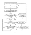
- FIG. 4 schematically shows a flow diagram of a method for determining an illumination intensity for inspection according to an embodiment.
- a method for determining an illumination intensity for inspection comprises the steps:
- At least one imaging element may take images of the object/sample to be inspected under illumination at a plurality of illumination intensities. If there are a plurality of imaging elements, the plurality of imaging elements are configured to take images of different regions of the object/sample to be inspected, respectively. For example, if there are five imaging elements, the five imaging elements are responsible for taking images of five different regions of the object/sample to be inspected, respectively.
- each of the plurality of imaging elements takes images of the sample to be inspected under illumination of the plurality of different illumination intensities to acquire a plurality of images of the sample to be inspected.
- each imaging element is responsible for taking images of different regions of the sample to be inspected.
- the imaging element may be configured to take images of the sample to be inspected through a reflective illumination mode, and may also be configured to take images of the sample to be inspected through a transmissive illumination mode.
- the illumination intensity may be set to be 0-255 levels to correspond to 0-255 gray levels of the image.
- the plurality of illumination intensities may be selected from the 0-255 levels.
- the illumination intensity may be gradually increased from 10 to 250 at a pitch of 10 to sequentially take an image of the sample to be inspected, and thus each imaging element may take 25 pictures.
- a larger gray standard deviation of the image indicates more detail information comprised in the image, and is more favorable to the inspection of the defects of the sample to be inspected. Therefore, in the embodiment described herein, the gray standard deviation of the image may be used as the basis for determining whether the illumination intensity is optimum.
- the gray standard deviation of each image may be calculated by the following equation:
- ⁇ is the standard deviation
- M and N represent the number of pixels in the x and y directions, respectively
- I (x, y) represents the gray value of a certain point on the image
- I 0 represents the average gray value of the image.
- the illumination intensity corresponding to the maximum gradation standard deviation can be determined as the illumination intensity of each imaging element for inspection.
- the optimum illumination intensity of each imaging element may be obtained.
- the hardware performance of each imaging element may not be exactly the same, the optimum illumination intensity of each imaging element may be different. If an optical inspection is performed on an object to be inspected, it is necessary to set respective illumination intensity for each imaging element.
- the illumination intensity for inspection may also be determined by the following steps:
- normalization step 431 normalizing the gray standard deviations for each imaging element
- ⁇ -I curve drawing step 432 for each imaging element, drawing a curve of normalized gray standard deviation vs. illumination intensity ( ⁇ -I curve);
- preferred illumination intensity range determination step 433 determining a preferred illumination intensity range of each imaging element according to corresponding relationship between the normalized gray standard deviations and the plurality of illumination intensities;
- intersection acquisition step 434 acquiring an intersection of the preferred illumination intensity ranges of the individual imaging elements.
- step 435 determining the illumination intensity of each imaging element for inspection according to the intersection acquired in step 434 .
- each imaging element may use the same illumination intensity for illumination when a batch inspection is performed on the objects to be inspected, without the need to set a different illumination intensity for each imaging element, which is simple in operation, and conducive to the unity of inspection standards.
- the normalization can be performed by the following equation:
- ⁇ is the normalized gray standard deviation of the image
- ⁇ is the gray standard deviation of the image
- ⁇ max is the maximum gray standard deviation corresponding to a single imaging element. It is to be understood that the gray standard deviations can also be normalized by other methods, for example normalizing with a logarithmic function or an arctangent function.
- a ⁇ -I curve can be drawn for each imaging element.
- FIG. 6 schematically shows a ⁇ -I curve of a single imaging element. As can be seen from FIG. 6 , the drawn ⁇ -I curve has a peak, so that the preferred illumination intensity for inspection can be determined according to the curve.
- the preferred illumination intensity range of each imaging element may be acquired from the ⁇ -I curve drawn in step 432 .
- a range between the illumination intensities corresponding to the normalized gray standard deviation that is equal to a predetermined value may be determined as the preferred illumination intensity range of each imaging element.
- the predetermined value may be set as a, where 0 ⁇ a ⁇ 1.
- the illumination intensity range between I 1 and I 2 is determined as the preferred illumination intensity range of the imaging element.
- when a 1, it only corresponds to one illumination intensity, and it may be considered that there is only one element in the preferred illumination intensity range.
- intersection acquisition step 434 the intersection of these preferred illumination intensity ranges are obtained according to the preferred illumination intensity ranges of the individual imaging elements acquired in the preferred illumination intensity determination step 433 .
- intersection may be acquired by the following steps:
- iii determining whether a is greater than a predetermined threshold b, where 0 ⁇ b ⁇ 1, and if so, executing step IV); otherwise, debugging the hardware of the apparatus for optical inspection;
- the individual imaging elements of the apparatus for optical inspection have the same or similar hardware configuration. If the value of a is reduced to sufficiently small, e.g., less than a predetermined threshold b, and there is still no intersection among the preferred illumination intensities of the individual imaging elements, it means that the hardware of the apparatus for optical inspection may be problematic, whereby it is necessary to debug the hardware. After debugging, the intersection may be acquired again by the above method so as to acquire the illumination intensity for inspection according to the intersection.
- the predetermined threshold is set to be 0.8.
- an intermediate value in the intersection of the preferred illumination intensity ranges of the respective imaging elements are determined as the illumination intensities of the individual imaging elements for inspection so that each imaging element uses the same illumination to take the images, thereby facilitating operations and the unity of inspection standards.
- the sample to be inspected may be a color film substrate, a thin film transistor (TFT) array substrate, or a printed circuit board (PCB) for a liquid crystal display.
- TFT thin film transistor
- PCB printed circuit board
- the illumination intensity for inspection may be determined using the method provided in the embodiments described herein, and then the illumination intensity may be used to inspect whether there are defects in the elements formed by the process, so as to repair the defects in time.
- the method provided in the embodiments described herein may be used to determine the illumination intensity for inspecting the black matrix, and then the determined illumination intensity may be used to inspect whether there are defects on the black matrix of the color film substrate so as to repair the defects of the black matrix in time; after a color filter is formed on the color film substrate, the method provided in the embodiments described in the present invention may be used to determine an illumination intensity for inspecting the color filter, and then the determined illumination intensity may be used to inspect whether there are defects in the color filter so as to repair the defects of the color filter in time.
- a defect inspection may be performed after each element (e.g., protective layer and columnar spacer, etc.) is formed sequentially so as to repair the defects in time when they exist.
- the illumination intensity for inspection may be determined according to the gray standard deviation of the image. As described above, the greater the gray standard deviation of the image, the more detailed information that the image contains, and the more helpful to the inspection of defects of the sample to be inspected. Therefore, the accuracy of inspection may be improved by using the illumination intensity determined by the method described in the embodiments herein to inspect the object to be inspected.
- FIG. 7 schematically shows a flow diagram of a method for optical inspection according to an embodiment.
- the illumination intensity inspection method comprises:
- step 72 in order to inspect the objects to be inspected, it is possible to first select one of the objects to be inspected as the sample to be inspected and then apply the method shown in FIGS. 4 to 6 to the sample to be inspected to determine the illumination intensity for inspection, so as to perform bulk optical inspection of the objects to be inspected by using the determined illumination intensity.
- the illumination intensity for inspection may be determined by using the same method as that described in the above embodiments and shown in FIGS. 4 to 6 , the explanations and descriptions of the method for determining the illumination intensity for inspection and the advantages thereof in the above-described embodiments with reference to FIGS. 4 to 6 , may also be applicable to the present embodiment.
- the inspection accuracy may be improved.
- the flow charts depicted herein are just one example. There may be many variations to these charts or the steps described therein without departing from the spirit of the disclosure. For instance, the steps may be performed in a differing order or steps may be added, deleted or modified.
- the normalization step 431 may be omitted and a curve of the gray standard deviation vs. illumination intensity may be drawn directly; and the curve of the gray standard deviation vs. illumination intensity may also be replaced with a corresponding table of the gray standard deviation vs. illumination intensity, all of which are considered a part of the claimed aspect.
- FIG. 8 schematically shows a block diagram of an apparatus for determining an illumination intensity for inspection according to an embodiment.
- the apparatus 80 for determining the illumination intensity for inspection comprises at least one imaging element 81 , an image acquisition unit 82 , a calculation unit 83 , and an illumination intensity determination unit 84 .
- the at least one imaging element 81 may be configured for taking an image of a sample to be inspected, and in particular, the at least one imaging element may be configured to take images of different regions of the sample to be inspected, respectively.
- the image acquisition unit 82 may be configured for acquiring images of the sample to be inspected taken by each imaging element at a plurality of illumination intensities.
- the calculation unit 83 may be configured for calculating a gray standard deviation of each of images acquired at a plurality of illumination intensities for each imaging element.
- the illumination intensity determination unit 84 may be configured for determining the illumination intensity of each imaging element for inspection according to the gradation standard deviations.
- the illumination intensity unit 84 may further comprise a normalization unit, a preferred illumination intensity range determination unit, an intersection acquisition unit, and an illumination intensity determination sub-unit, wherein the normalization unit is configured for normalizing the gray standard deviations of each imaging element; the preferred illumination intensity range determination unit is configured for determining a preferred illumination intensity range of each imaging element according to the normalized gray standard deviations and a corresponding relationship between the normalized gray standard deviations and the plurality of illumination intensities; the intersection acquisition unit is configured for acquiring an intersection of the preferred illumination intensity ranges of the at least one imaging element; and the illumination intensity determination subunit is configured for determining, according to the intersections, the illumination intensity of each imaging element for inspection.
- the normalization unit is configured for normalizing the gray standard deviations of each imaging element
- the preferred illumination intensity range determination unit is configured for determining a preferred illumination intensity range of each imaging element according to the normalized gray standard deviations and a corresponding relationship between the normalized gray standard deviations and the plurality of illumination intensities
- the intersection acquisition unit is configured for acquiring
- the preferred illumination intensity range determination unit may be further configured for determining a range of the illumination intensities corresponding to the normalized gray standard deviation that is equal to a predetermined value as the preferred illumination intensity range of each imaging element.
- the intersection acquisition unit may be further configured for determining whether there is an intersection among the preferred illumination intensity ranges of the individual imaging elements, and if so, acquiring the intersection among the preferred illumination intensity ranges of the at least one imaging element; otherwise, gradually reducing the predetermined value until there is an intersection among the acquired preferred illumination intensity ranges of the imaging elements.
- the predetermined value is no less than 0.8.
- the illumination intensity determination sub-unit may be further configured for determining an intermediate value in the intersection as the illumination intensity of each imaging element for inspection.
- the illumination intensity determination unit 84 may be further configured for determining, for each imaging element, the illumination intensity corresponding to the largest gray standard deviation among the gray standard deviations as the illumination intensity of each imaging element for inspection.
- the apparatus for determining the illumination intensity for inspection may determine the illumination intensity for inspection.
- the method for determining the illumination intensity for inspection described in the embodiments abovementioned and shown in FIGS. 4-6 may be used to determine the illumination intensity for inspection. Therefore, the explanations and descriptions of the method for determining the illumination intensity for inspection and the advantages thereof in the above-described embodiments with reference to FIGS. 4 to 6 , are also applicable to the present embodiment.
- an apparatus for optical inspection configured for performing an automated optical inspection on an object to be inspected.
- the apparatus for optical inspection comprises the apparatus for determining the illumination intensity for inspection as provided by preceding embodiments.
- the apparatus for optical inspection comprises the apparatus for determining the illumination intensity for inspection as provided by preceding embodiments
- the explanations and descriptions of the apparatus for determining the illumination intensity for inspection in the preceding embodiments are also applicable to the present embodiment.
- the units or modules such as the image acquisition unit, the calculation unit, the illumination intensity determination unit, the normalization unit, the preferred illumination intensity range determination unit, the intersection acquisition unit, and the illumination intensity determination sub-unit described herein may be implemented as a combination of a processor and a memory, wherein the processor executes a program stored in the memory to implement the functionality of the corresponding units or modules.
- the units or modules describes herein may also be completely implemented by hardware, including but not limited to Application Specific Integrated Circuits (ASICs), Field Programmable Gate Arrays (FPGAs).
- ASICs Application Specific Integrated Circuits
- FPGAs Field Programmable Gate Arrays
- a protective layer on a color film substrate is inspected by an apparatus for automated optical inspection having 19 reflective cameras, to determine an illumination intensity for inspection. Further, the determined illumination intensity may be used for batch inspection of the protective layer on the color film substrate.
- FIG. 9 schematically shows a flow diagram of a method for determining an illumination intensity for inspection in the example.
- the illumination intensity is set to gradually increase from 10 to 250 at a pitch of 10, in which case each camera can take 25 images at 25 different illumination intensities.
- the method for determining the illumination intensity for inspection comprises the following steps:
- step 91 collect images of a sample to be inspected taken by the 19 cameras at different reflective illumination intensities
- step 92 for each camera, calculating a gray standard deviation of each image by image processing software
- step 93 for each camera, drawing a curve of gray standard deviation vs. illumination intensity
- the gray scale standard deviation may be normalized, in which case the curve of the normalized gray standard deviation vs. illumination intensity ( ⁇ -I curve) may be drawn.
- FIG. 10 shows the ⁇ -I curves corresponding to the cameras 1 , 3 , 7 , 11 , 15 , and 19 respectively.
- the vertical ordinate represents the normalized gray standard deviation and the abscissa represents the illumination intensity.
- step 95 reducing the value of a by a pitch of 0.02;
- step 96 determining whether a is less than a predetermined threshold (e.g., 0.8), if so, debugging the apparatus, and then returning to step 91 ; if not, executing step 97 ;
- a predetermined threshold e.g. 0.
- a is less than a predetermined threshold, and no intersection is found, it means that there may be a problem with the apparatus, which may be debugged, such as by adjusting the focus position of the camera lens, adjusting the camera gain, and so on.
- Using the illumination intensity to perform an automated optical inspection on the object to be inspected may improve the inspection accuracy.
Abstract
Description
-
- image acquisition step 41: acquiring images of different regions of the sample to be inspected taken by each imaging element at a plurality of illumination intensities;
- gray standard deviation calculation step 42: calculating, for each imaging element, a gray standard deviation of each of the images acquired at the plurality of illumination intensities; and
- illumination intensity determination step 43: determining the illumination intensity of each imaging element for inspection according to the gray standard deviations.
Claims (14)
Applications Claiming Priority (4)
| Application Number | Priority Date | Filing Date | Title |
|---|---|---|---|
| CN201610342920.0A CN105911724B (en) | 2016-05-23 | 2016-05-23 | Determine the method and apparatus of the intensity of illumination for detection and optical detecting method and device |
| CN201610342920 | 2016-05-23 | ||
| CN201610342920.0 | 2016-05-23 | ||
| PCT/CN2017/076916 WO2017202114A1 (en) | 2016-05-23 | 2017-03-16 | Method and apparatus for determining illumination intensity for inspection, and optical inspection method and apparatus |
Publications (2)
| Publication Number | Publication Date |
|---|---|
| US20180158185A1 US20180158185A1 (en) | 2018-06-07 |
| US10510141B2 true US10510141B2 (en) | 2019-12-17 |
Family
ID=56749733
Family Applications (1)
| Application Number | Title | Priority Date | Filing Date |
|---|---|---|---|
| US15/552,126 Expired - Fee Related US10510141B2 (en) | 2016-05-23 | 2017-03-16 | Method and apparatus for determining illumination intensity for inspection, and method and apparatus for optical inspection |
Country Status (3)
| Country | Link |
|---|---|
| US (1) | US10510141B2 (en) |
| CN (1) | CN105911724B (en) |
| WO (1) | WO2017202114A1 (en) |
Cited By (1)
| Publication number | Priority date | Publication date | Assignee | Title |
|---|---|---|---|---|
| US11022562B2 (en) * | 2019-04-15 | 2021-06-01 | Illinois Tool Works Inc. | Methods and systems for vision system assisted inspections |
Families Citing this family (5)
| Publication number | Priority date | Publication date | Assignee | Title |
|---|---|---|---|---|
| CN105911724B (en) | 2016-05-23 | 2018-05-25 | 京东方科技集团股份有限公司 | Determine the method and apparatus of the intensity of illumination for detection and optical detecting method and device |
| CN109949725B (en) * | 2019-03-06 | 2022-09-20 | 武汉精立电子技术有限公司 | Image gray level standardization method and system for AOI system |
| CN110132976B (en) * | 2019-04-23 | 2022-03-25 | 合刃科技(深圳)有限公司 | Detection method and detection device |
| CN114450580A (en) * | 2019-10-02 | 2022-05-06 | 柯尼卡美能达株式会社 | Workpiece surface defect detection device and detection method, workpiece surface inspection system, and program |
| KR20230067759A (en) * | 2021-11-08 | 2023-05-17 | 삼성디스플레이 주식회사 | optical inspection device and inspecting method using the same |
Citations (14)
| Publication number | Priority date | Publication date | Assignee | Title |
|---|---|---|---|---|
| US6627863B2 (en) * | 2000-12-15 | 2003-09-30 | Mitutoyo Corporation | System and methods to determine the settings of multiple light sources in a vision system |
| US20040178351A1 (en) * | 2003-03-14 | 2004-09-16 | Kim Deok-Yong | Method of optimizing focus of optical inspection apparatus and method and apparatus of detecting defects using the same |
| JP2007043439A (en) | 2005-08-03 | 2007-02-15 | Casio Comput Co Ltd | White balance adjustment apparatus and method |
| US20070258070A1 (en) * | 2004-07-12 | 2007-11-08 | Nikon Corporation | Method for Determining Exposure Condition, Exposure Method, Exposure Apparatus, and Method for Manufacturing Device |
| CN101419176A (en) | 2007-10-26 | 2009-04-29 | 比亚迪股份有限公司 | Surface flaw detecting method and device |
| CN101556380A (en) | 2008-04-08 | 2009-10-14 | 东捷科技股份有限公司 | Optical source correcting method |
| CN101676695A (en) | 2008-09-16 | 2010-03-24 | 中茂电子(深圳)有限公司 | Image detection system and method capable of detection by appropriate brightness |
| US20110103679A1 (en) * | 2009-10-29 | 2011-05-05 | Mitutoyo Corporation | Autofocus video tool and method for precise dimensional inspection |
| US20130033620A1 (en) * | 2011-08-05 | 2013-02-07 | Quality Vision International, Inc. | Method for automatically adjusting the levels of illumination sources in an optical measurement machine |
| CN103905731A (en) | 2014-03-26 | 2014-07-02 | 武汉烽火众智数字技术有限责任公司 | Broadband dynamic image collection method and system |
| JP2014211411A (en) | 2013-04-22 | 2014-11-13 | 凸版印刷株式会社 | Dark field optical system defect inspection device |
| US20160148073A1 (en) * | 2013-06-27 | 2016-05-26 | Robert Bosch Gmbh | Inspection of the contoured surface of the undercarriage of a motor vehicle |
| CN105911724A (en) | 2016-05-23 | 2016-08-31 | 京东方科技集团股份有限公司 | Method and device for determining illumination intensity for detection and optical detection method and device |
| US20170262968A1 (en) * | 2014-09-15 | 2017-09-14 | Carl Zeiss Microscopy Gmbh | Method for Generating a Result Image and Optical Device |
-
2016
- 2016-05-23 CN CN201610342920.0A patent/CN105911724B/en not_active Expired - Fee Related
-
2017
- 2017-03-16 US US15/552,126 patent/US10510141B2/en not_active Expired - Fee Related
- 2017-03-16 WO PCT/CN2017/076916 patent/WO2017202114A1/en active Application Filing
Patent Citations (14)
| Publication number | Priority date | Publication date | Assignee | Title |
|---|---|---|---|---|
| US6627863B2 (en) * | 2000-12-15 | 2003-09-30 | Mitutoyo Corporation | System and methods to determine the settings of multiple light sources in a vision system |
| US20040178351A1 (en) * | 2003-03-14 | 2004-09-16 | Kim Deok-Yong | Method of optimizing focus of optical inspection apparatus and method and apparatus of detecting defects using the same |
| US20070258070A1 (en) * | 2004-07-12 | 2007-11-08 | Nikon Corporation | Method for Determining Exposure Condition, Exposure Method, Exposure Apparatus, and Method for Manufacturing Device |
| JP2007043439A (en) | 2005-08-03 | 2007-02-15 | Casio Comput Co Ltd | White balance adjustment apparatus and method |
| CN101419176A (en) | 2007-10-26 | 2009-04-29 | 比亚迪股份有限公司 | Surface flaw detecting method and device |
| CN101556380A (en) | 2008-04-08 | 2009-10-14 | 东捷科技股份有限公司 | Optical source correcting method |
| CN101676695A (en) | 2008-09-16 | 2010-03-24 | 中茂电子(深圳)有限公司 | Image detection system and method capable of detection by appropriate brightness |
| US20110103679A1 (en) * | 2009-10-29 | 2011-05-05 | Mitutoyo Corporation | Autofocus video tool and method for precise dimensional inspection |
| US20130033620A1 (en) * | 2011-08-05 | 2013-02-07 | Quality Vision International, Inc. | Method for automatically adjusting the levels of illumination sources in an optical measurement machine |
| JP2014211411A (en) | 2013-04-22 | 2014-11-13 | 凸版印刷株式会社 | Dark field optical system defect inspection device |
| US20160148073A1 (en) * | 2013-06-27 | 2016-05-26 | Robert Bosch Gmbh | Inspection of the contoured surface of the undercarriage of a motor vehicle |
| CN103905731A (en) | 2014-03-26 | 2014-07-02 | 武汉烽火众智数字技术有限责任公司 | Broadband dynamic image collection method and system |
| US20170262968A1 (en) * | 2014-09-15 | 2017-09-14 | Carl Zeiss Microscopy Gmbh | Method for Generating a Result Image and Optical Device |
| CN105911724A (en) | 2016-05-23 | 2016-08-31 | 京东方科技集团股份有限公司 | Method and device for determining illumination intensity for detection and optical detection method and device |
Non-Patent Citations (3)
| Title |
|---|
| International Search Report from corresponding PCT Application No. PCT/CN2017/076916 dated Jun. 20, 2017 (5 pages). |
| Office Action from corresponding Chinese Application No. 201610342920.0 dated Aug. 25, 2017 (6 pages). |
| Written Opinion from corresponding PCT Application No. PCT/CN2017/076916 dated Jun. 20, 2017 (5 pages). |
Cited By (1)
| Publication number | Priority date | Publication date | Assignee | Title |
|---|---|---|---|---|
| US11022562B2 (en) * | 2019-04-15 | 2021-06-01 | Illinois Tool Works Inc. | Methods and systems for vision system assisted inspections |
Also Published As
| Publication number | Publication date |
|---|---|
| CN105911724A (en) | 2016-08-31 |
| CN105911724B (en) | 2018-05-25 |
| WO2017202114A1 (en) | 2017-11-30 |
| US20180158185A1 (en) | 2018-06-07 |
Similar Documents
| Publication | Publication Date | Title |
|---|---|---|
| US10510141B2 (en) | Method and apparatus for determining illumination intensity for inspection, and method and apparatus for optical inspection | |
| CN104484878B (en) | The automatic testing method of defects of display panel | |
| Jiang* et al. | Liquid crystal display surface uniformity defect inspection using analysis of variance and exponentially weighted moving average techniques | |
| CN112070762A (en) | Mura defect detection method and device for liquid crystal panel, storage medium and terminal | |
| CN109712115B (en) | Automatic PCB detection method and system | |
| CN115147362A (en) | Detection method, detection device and detection system for display panel | |
| JP2007086534A (en) | Image correction device, pattern inspection device, image correction method, and pattern inspection method | |
| CN109426013B (en) | Method and device for analyzing and detecting and repairing defects of color film substrate | |
| US8842270B2 (en) | Method and inspection device for bright spot defect detection of a polarizer | |
| US7538750B2 (en) | Method of inspecting a flat panel display | |
| US20210082120A1 (en) | Repairing method for mura in display panel | |
| CN117589770A (en) | PCB patch board detection method, device, equipment and medium | |
| CN106733549B (en) | Membrane layer repairing method and system | |
| JP6515348B2 (en) | Calibration plate for surface inspection apparatus and calibration method for surface inspection apparatus | |
| CN109751959B (en) | Line width measuring method | |
| JP4664417B2 (en) | Display panel lighting inspection device and display panel lighting inspection method. | |
| WO2017049863A1 (en) | Liquid crystal one drop filling system and control method | |
| TWI695969B (en) | Inspecting system and method for light emitting source | |
| US20100250193A1 (en) | System and method for testing liquid crystal display device | |
| US20140168643A1 (en) | Method for inspecting defects of optical layer elements of a display device | |
| TWI672493B (en) | An automatic optical inspection system and method to obtain mura defect from the panel | |
| CN107731704B (en) | Method and device for detecting reverse angle of via hole | |
| CN110874837A (en) | Automatic defect detection method based on local feature distribution | |
| US20180306725A1 (en) | Dynamic color filter macroscopic inspection system and method | |
| KR20190016368A (en) | Inspection method for edge of flat panel display and recording medium |
Legal Events
| Date | Code | Title | Description |
|---|---|---|---|
| AS | Assignment |
Owner name: CHONGQING BOE OPTOELECTRONICS TECHNOLOGY CO., LTD. Free format text: ASSIGNMENT OF ASSIGNORS INTEREST;ASSIGNOR:WANG, XU;REEL/FRAME:043367/0320 Effective date: 20170731 Owner name: BOE TECHNOLOGY GROUP CO., LTD., CHINA Free format text: ASSIGNMENT OF ASSIGNORS INTEREST;ASSIGNOR:XI, ZHENGDONG;REEL/FRAME:043367/0463 Effective date: 20170731 Owner name: CHONGQING BOE OPTOELECTRONICS TECHNOLOGY CO., LTD. Free format text: ASSIGNMENT OF ASSIGNORS INTEREST;ASSIGNOR:LIU, CHAOQIANG;REEL/FRAME:043367/0428 Effective date: 20170731 Owner name: CHONGQING BOE OPTOELECTRONICS TECHNOLOGY CO., LTD. Free format text: ASSIGNMENT OF ASSIGNORS INTEREST;ASSIGNOR:LIU, YANG;REEL/FRAME:043367/0495 Effective date: 20170731 Owner name: BOE TECHNOLOGY GROUP CO., LTD., CHINA Free format text: ASSIGNMENT OF ASSIGNORS INTEREST;ASSIGNOR:WANG, XU;REEL/FRAME:043367/0320 Effective date: 20170731 Owner name: BOE TECHNOLOGY GROUP CO., LTD., CHINA Free format text: ASSIGNMENT OF ASSIGNORS INTEREST;ASSIGNOR:LIU, YANG;REEL/FRAME:043367/0495 Effective date: 20170731 Owner name: CHONGQING BOE OPTOELECTRONICS TECHNOLOGY CO., LTD. Free format text: ASSIGNMENT OF ASSIGNORS INTEREST;ASSIGNOR:XI, ZHENGDONG;REEL/FRAME:043367/0463 Effective date: 20170731 Owner name: BOE TECHNOLOGY GROUP CO., LTD., CHINA Free format text: ASSIGNMENT OF ASSIGNORS INTEREST;ASSIGNOR:LIU, CHAOQIANG;REEL/FRAME:043367/0428 Effective date: 20170731 |
|
| STPP | Information on status: patent application and granting procedure in general |
Free format text: NON FINAL ACTION MAILED |
|
| STPP | Information on status: patent application and granting procedure in general |
Free format text: RESPONSE TO NON-FINAL OFFICE ACTION ENTERED AND FORWARDED TO EXAMINER |
|
| STPP | Information on status: patent application and granting procedure in general |
Free format text: NOTICE OF ALLOWANCE MAILED -- APPLICATION RECEIVED IN OFFICE OF PUBLICATIONS |
|
| STPP | Information on status: patent application and granting procedure in general |
Free format text: PUBLICATIONS -- ISSUE FEE PAYMENT VERIFIED |
|
| STCF | Information on status: patent grant |
Free format text: PATENTED CASE |
|
| FEPP | Fee payment procedure |
Free format text: PETITION RELATED TO MAINTENANCE FEES GRANTED (ORIGINAL EVENT CODE: PTGR); ENTITY STATUS OF PATENT OWNER: LARGE ENTITY |
|
| FEPP | Fee payment procedure |
Free format text: MAINTENANCE FEE REMINDER MAILED (ORIGINAL EVENT CODE: REM.); ENTITY STATUS OF PATENT OWNER: LARGE ENTITY |
|
| LAPS | Lapse for failure to pay maintenance fees |
Free format text: PATENT EXPIRED FOR FAILURE TO PAY MAINTENANCE FEES (ORIGINAL EVENT CODE: EXP.); ENTITY STATUS OF PATENT OWNER: LARGE ENTITY |
|
| STCH | Information on status: patent discontinuation |
Free format text: PATENT EXPIRED DUE TO NONPAYMENT OF MAINTENANCE FEES UNDER 37 CFR 1.362 |
|
| FP | Lapsed due to failure to pay maintenance fee |
Effective date: 20231217 |